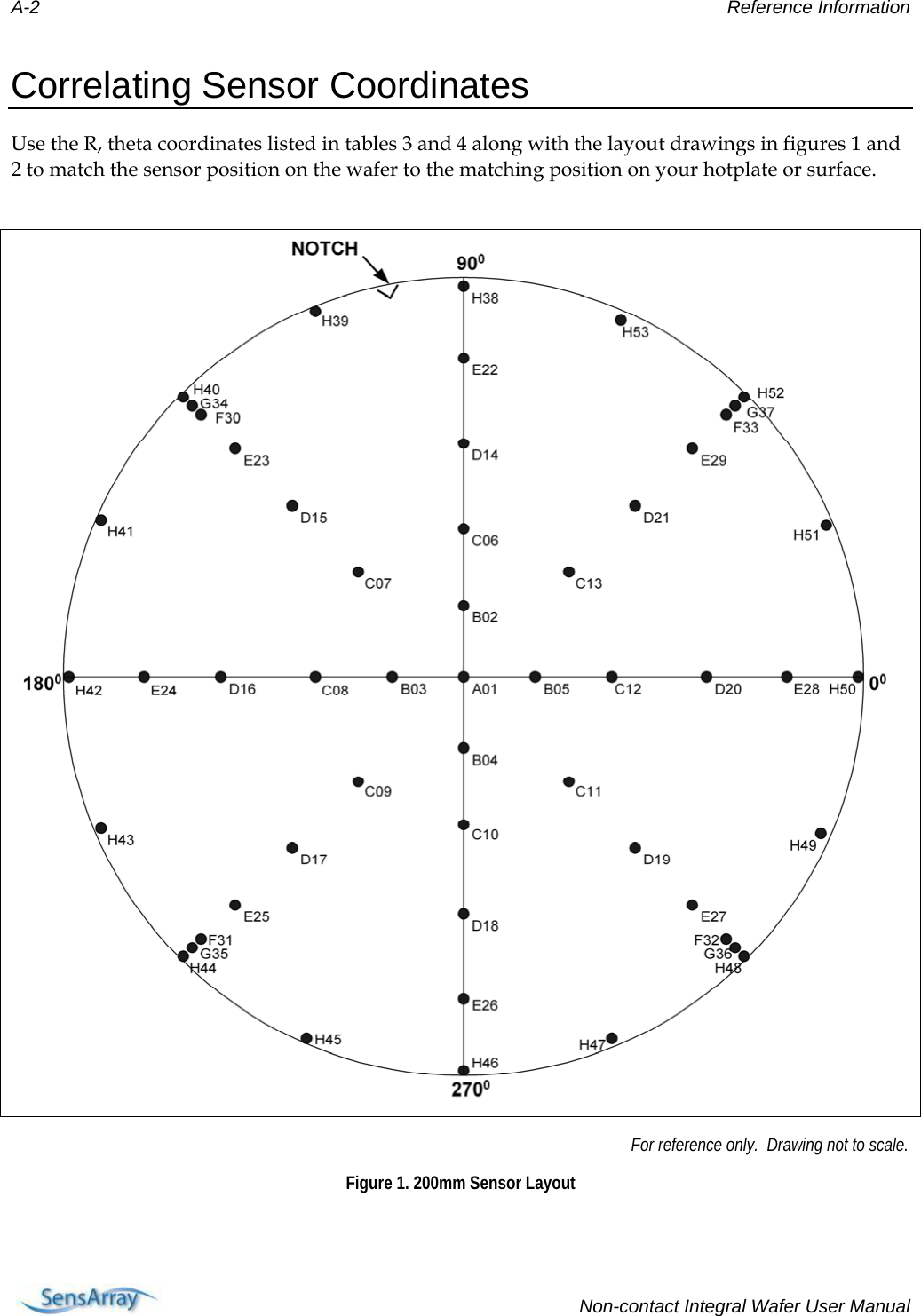
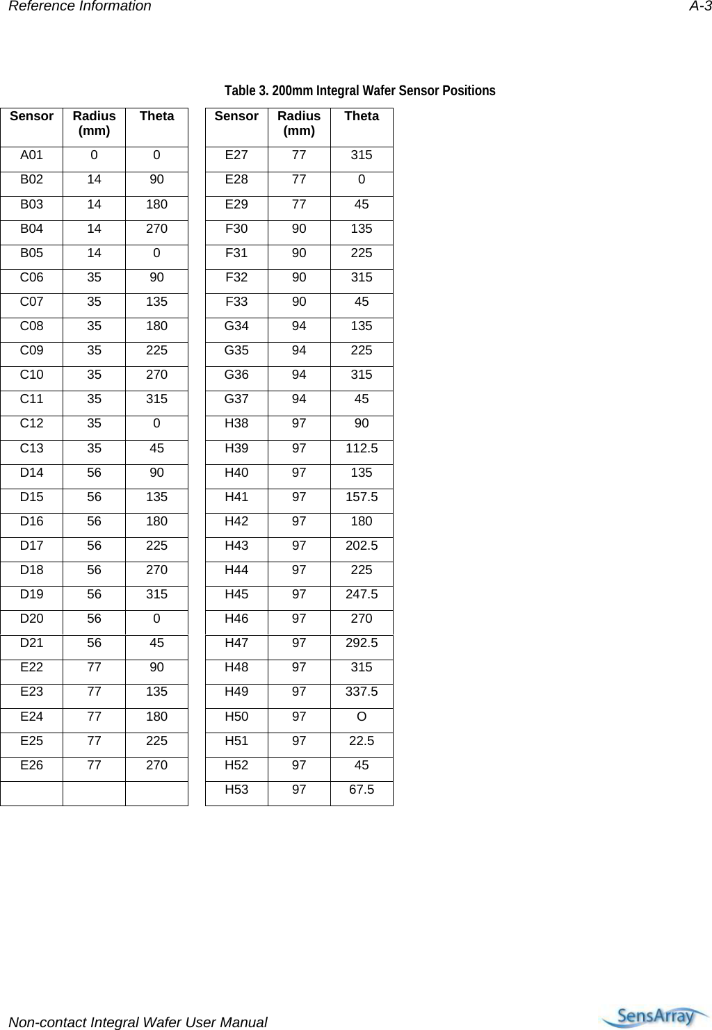
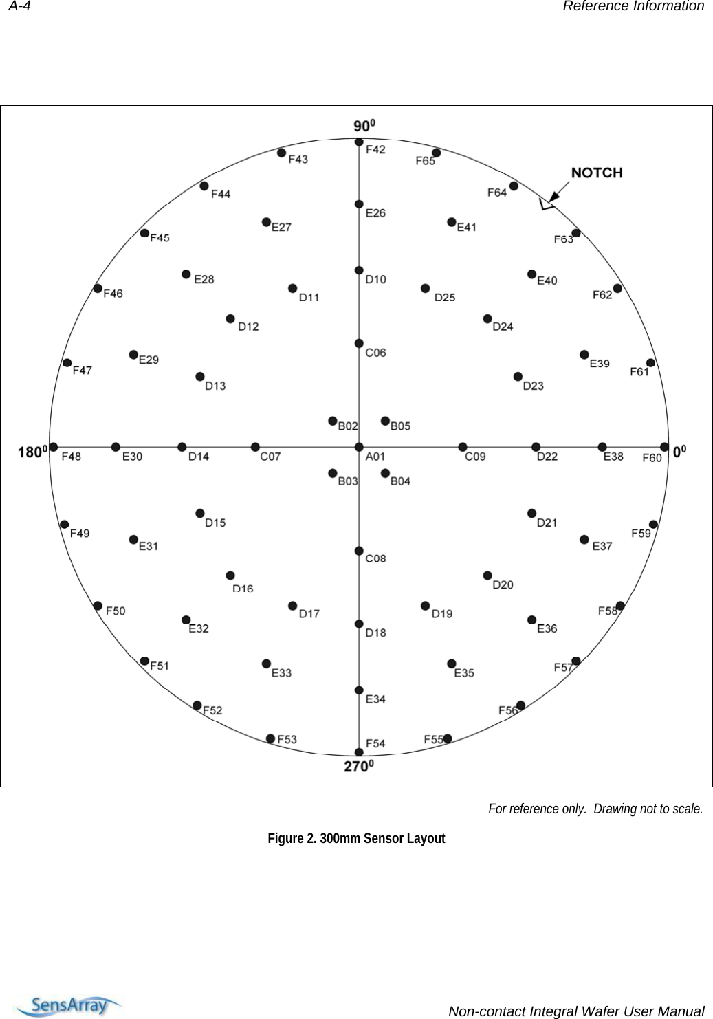
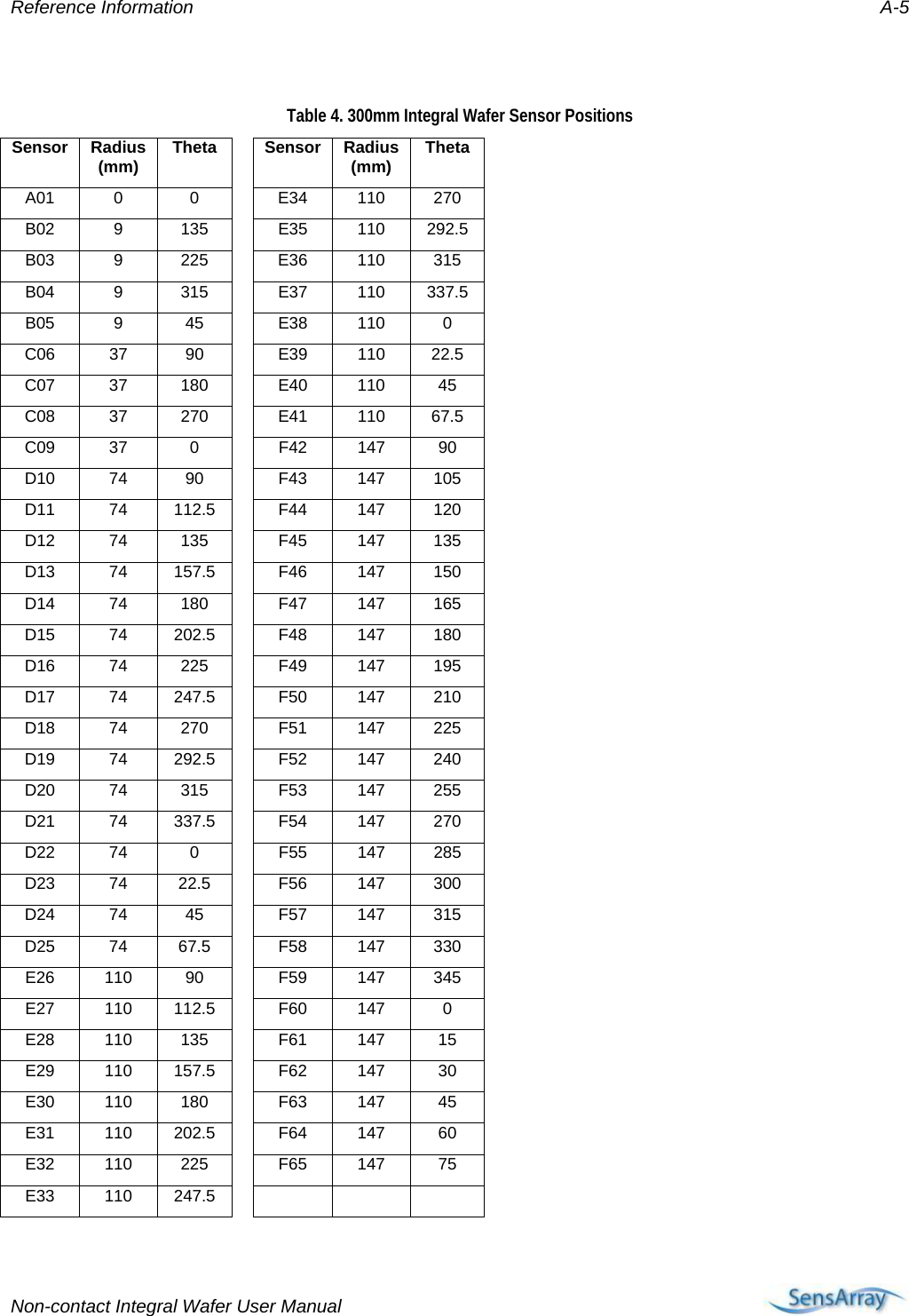
KLA RFWC812A Integral Wafer RF Carrier System for 200 and 300mm Wafers User Manual Integral Wafer NC Title Page

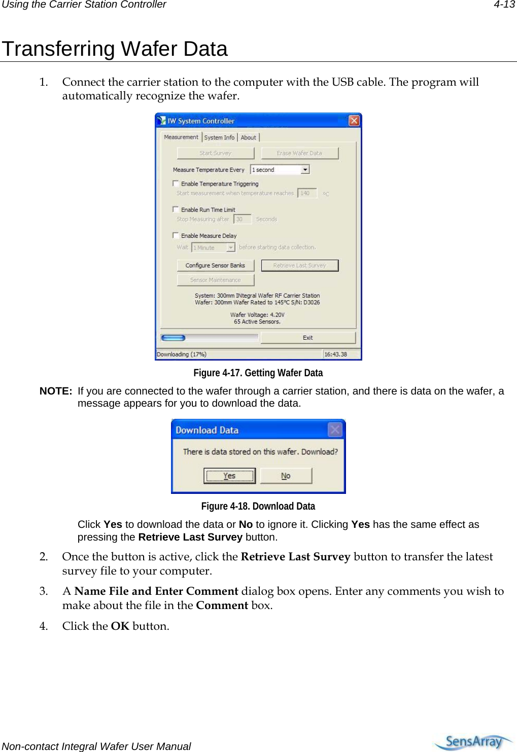
KLA-Tencor Corporation Integral Wafer RF Carrier System for 200 and 300mm Wafers Integral Wafer NC Title Page

Contents

Users Manual 2

Non-Contact Integral Wafer™ User Manual                   5451 Patrick Henry Dr. Santa Clara, CA 95054  408-986-5600 Fax 408-986-5601 info@sensarray.com www.sensarray.com
Copyright © 2006 by °SensArray® Corporation. All rights reserved.                            UM-INT- 2007.04  SensArray reserves the right to modify, change, or improve any or  all specifications published in this document without notice.
 Important Notices Warranty Integral Wafer System Hardware SensArray Corporation warrants that the contact style or non-contact style Integral Wafer Systems (“Products”) sold will be free from defects in material and workmanship, and perform to SensArray’s applicable published specifications for a period of 12 months after shipment for the Docking Station. The Integral Wafer is warranted for 6 months or a specified number of operating hours, whichever occurs first. Refer to the specification provided with your wafer for the exact warranty terms. The Products that comprise the System shall include the Docking Station. The liability of SensArray hereunder shall be limited to replacing or repairing, at its option, any defective Products that are returned F.O.B. to SensArray’s plant in Santa Clara, CA. In no case are Products to be returned without the purchaser first obtaining SensArray’s permission and Returned Materials Authorization [RMA] number. In no event shall SensArray be liable for any consequential or incidental damages. Products that have been subject to abuse, misuse, accident, alteration, neglect, or unauthorized repair or installation are not covered by this warranty. SensArray will make the final determination as to the existence and cause of any alleged defect. SensArray is not responsible for maintaining or supplying any consumable materials used in conjunction with this hardware. No warranty is made with respect to any customized equipment or Products supplied with Integral Wafer systems where produced to Purchaser’s specifications except as specifically stated in writing by SensArray in the contract for such Products. The purchaser will pay the shipping costs of returned materials to SensArray; SensArray will pay the cost of shipping repaired/replaced material to Purchaser. This Warranty is the only warranty made by SensArray with respect to the Product delivered hereunder and may be modified only by a written instrument that is signed by a duly authorized officer of SensArray and accepted by Purchaser. Except as provided above, SensArray makes no warrantees, expressed or implied, including any warranty of merchantability for a particular purpose. Integral Wafer Software SensArray Corporation warrants that (a) Integral Wafer software (Software) will perform substantially in accordance with the accompanying written materials for a period of 12 months after shipment, and (b) the medium on which the Software is recorded will be free from defects in materials and workmanship under normal use and service for a period of 12 months after shipment. Faults caused by unauthorized modification, misuse or abuse of products, or problems due to software not supplied by SensArray, are not covered by this Warranty. During the Warranty Period, the purchaser may return failed Software to SensArray for repair or replacement, at SensArray’s option. SensArray does not warrant that the operation of the Software shall be uninterrupted or error free. The purchaser will first notify SensArray of the nature of the problem and obtain a Returned Materials Authorization [RMA] number. The purchaser will pay the costs of shipping returned Software to SensArray; SensArray will pay the cost of shipping repaired/replaced Software to the purchaser. No other warranty is expressed or implied. SensArray specifically disclaims the implied warranty of merchantability and fitness for a specific application. The Integral Wafer Software Documentation Materials (“Documentation”) are subject to revision and change without notice. SensArray agrees to make a best effort attempt to keep the purchaser advised of changes to the Documentation.
Software License Agreement The Software is owned by SensArray Corporation and is protected by United States copyright laws and international treaty provisions. Therefore, you must treat the Software like any other copyrighted material. Under the Copyright Laws, the Integral Wafer Software, or accompanying written materials, may not be copied, photo-copied, reproduced, translated, in whole or in part, without the prior written permission of SensArray.  You may make one copy of the Software solely for backup or archival purposes. You may make 10 copies of the written materials accompanying the SensArray Corporation-produced Software provided that such copies are solely for use by personnel using the Integral Wafer System. All rights not expressly granted to you in this Agreement are reserved to SensArray Corporation. Third-Party Software Licenses for any software which was provided but not produced by SensArray Corporation are granted solely and only by the original supplier or manufacturer and solely and only with the supplier’s limitations and rights. Copying restrictions for such software are governed solely and only by the original supplier or manufacturer’s license or any other supplier-approved agreements, as applicable. Trademarks °SensArray®, Thermal MAP, Integral Wafer™, and Process Probe® are trademarks of SensArray Corporation.  Windows and Excel are trademarks or trade names of Microsoft Corporation.  Any other terms mentioned in this document that are known to be trademarks or service marks have been appropriately capitalized. Use of a term in this document should not be regarded as affecting the validity of any trademark or service mark. Some of the technology used in this product is acquired under license from the management and operating contractor of the Oak Ridge National Laboratory on behalf of the U.S. Department of Energy.
Radio Frequency Interference Compliance Applies to the Storage Cases and RF Carrier Station NOTE: This equipment has been tested and found to comply with the limits for a Class A digital device, pursuant to part 15 of the FCC Rules. These limits are designed to provide reasonable protection against harmful interference when the equipment is operated in a commercial environment. This equipment generates, uses, and can radiate radio frequency energy and, if not installed and used in accordance with the instruction manual, may cause harmful interference to radio communications. Operation of this equipment in a residential area is likely to cause harmful interference in which case the user will be required to correct the interference at his own expense.  For the RF Carrier Station, only the USB cable supplied with the equipment is authorized for use with this device; any other cable is not authorized and may cause undesired interference, etc. Refer to Chapter 3 for product installation. RF Carrier Station USB Cable  Product Modifications  Applies to the Storage Cases and RF Carrier Station Changes or modifications to this equipment not expressly approved by KLA-Tencor may void the user’s authority to operate the equipment.   English French This device complies with Industry Canada licence-exempt RSS standard(s). Operation is subject to the following two conditions: (1) this device may not cause interference, and (2) this device must accept any interference, including interference that may cause undesired operation of the device. Le présent appareil est conforme aux CNR d'Industrie Canada applicables aux appareils radio exempts de licence. L'exploitation est autorisée aux deux conditions suivantes : (1) l'appareil ne doit pas produire de brouillage, et (2) l'utilisateur de l'appareil doit accepter tout brouillage radioélectrique subi, même si le brouillage est susceptible d'en compromettre le fonctionnement. 
Table of Contents i   Non-contact  Integral Wafer User Manual  Using This Manual ..................................................................................................................iii Overview.......................................................................................................................................... iii What You Need to Know................................................................................................................. iii Conventions Used in this Manual.....................................................................................................iv Chapter 1 Overview ..............................................................................................................1-1 The Integral Wafer System ............................................................................................................ 1-1 Acquiring Data............................................................................................................................... 1-1 Analyzing Data .............................................................................................................................. 1-2 Chapter 2  System Setup .................................................................................................2-1 Before You Begin .......................................................................................................................... 2-1 Proper Wafer Handling Procedures........................................................................................... 2-1 Unpacking Your System................................................................................................................ 2-2 Removing the Wafer from the Storage Case............................................................................. 2-2 Charging the Equipment Before Use ........................................................................................ 2-4 Setting Up the Software................................................................................................................. 2-4 Preparing Equipment for the Cleanroom ....................................................................................... 2-5 Cleaning the Equipment............................................................................................................ 2-5 Cleaning the Integral Wafer...................................................................................................... 2-5 Cleaning the Carrier Station...................................................................................................... 2-6 Chapter 3 Using the Charge and Communication Carrier Station .................................3-1 Using the Carrier Station................................................................................................................ 3-1 Removing the Wafer from the Carrier Station............................................................................... 3-6 Using the Wafer with the Carrier Station....................................................................................... 3-7 Chapter 4 Using the Integral Wafer System Controller Software ...................................4-1 Starting the Program ...................................................................................................................... 4-1 Wafer Time Limit Feature ............................................................................................................. 4-7 Defining a Survey .......................................................................................................................... 4-9 Transferring Wafer Data.............................................................................................................. 4-13  Appendix A   Reference Information ................................................................................A-1 Sensor Bank Reference ................................................................................................................. A-1 Correlating Sensor Coordinates .................................................................................................... A-2
iii  UUssiinngg  TThhiiss  MMaannuuaall  Overview This manual consists of the following sections. • Chapter 1, Overview—Discusses features, components, and configurations of the Non-contact Integral Wafer System. • Chapter 2, System Setup—Discusses unpacking the system components, preparing the equipment for the cleanroom, and connecting the system cables. • Chapter 3, Using the Charge and Communication Carrier Station— provides an easy means to prepare the wafer for data acquisition and to perform data retrieval. • Chapter 4, Using the Integral Wafer Controller Software— Discusses acquisition setup, acquisition features, and how to retrieve the measurement data using the Carrier Stations. • Appendix A, Reference Information- Wafer sensor location information. What You Need to Know This user manual assumes that you are familiar with the version of the Windows operating system installed on your computer and can perform—as a minimum—the following tasks. • Start (boot) the computer • Log on to Windows • Select from menus • Select and open files • Use a mouse or pointer, including how to point and click to select objects and operate controls such as buttons • Use standard window controls such as scroll bars Non-contact Integral Wafer User Manual
iv Using This Manual Conventions Used in this Manual Several standard conventions are used in the text of this manual to make the information presented a little clearer and easier to understand. Every attempt is made to be consistent in the application of these conventions.   Note:  Highlights important information. Bold  Bold text indicates button names, icon names, and menu items. italic  Italic text indicates the section and/or chapter name in a cross-reference. For example: See the Using the Acquisition Setup Window section of Chapter 3, Acquiring Data, for more information. Italic text can also be used to emphasize a word or phrase. Courier Typeface Courier typeface indicates file names, directories, and text that you enter. For example: The file is located in the C:\Sensarray\Configs directory. <Key>  A word offset by angle brackets indicates a key on the computer keyboard. For example: After you specify the parameters, press the <Enter> key. » The twin arrow symbol indicates menu navigation. For example: Select Acquisition»Acquire on the Thermal MAP Analysis window to open the Acquisition Setup window. This tells you to click on Acquisition on the menu bar and then click on the Acquire option from the drop-down menu.  Indicates important safety information. The icon is usually associated with a Warning or Caution in the document describing potential for product damage or personal injury. Other international standard icons specific to a particular hazard or action may be used in place of the exclamation mark.       Non-contact Integral Wafer User Manual
 1-1  Chapter 1  Overview The Integral Wafer User Manual is designed to document the setup and use of the Integral Wafer system in conjunction with the Integral Wafer Controller software. This manual will discuss only the non-contact version of the Integral Wafer. The results of the measurement run may be analyzed using the Thermal MAP Analysis Software included with the system. The Thermal MAP Analysis software program is documented in the Thermal MAP Analysis Software User Manual. A PDF version of this manual may be found in the C:\Sensarray\ Documents folder on your computer’s hard drive. This chapter discusses the features of the non-contact Integral Wafer system. The Integral Wafer System The Integral Wafer has a complete measurement system embedded in the wafer to record thermal surveys in semiconductor processing equipment without the need for wired connections. Embedding the components within the wafer allows it to be treated like a production wafer in most equipment, as long as it is within the operating temperature range of the wafer.  The Integral Wafer system consists of an Integral Wafer, a carrier station for communicating with and recharging the wafer, a USB cable, a laptop computer, and a CD containing the software and drivers needed by the system.  The Integral Wafer system is delivered with a SensArray-provided laptop computer pre-loaded with all software. As an option, existing Thermal MAP laptop computer systems may be upgraded to run the Integral Wafer software as long as you are running Windows 2000 or higher, and have an available USB port. Integral Wafer systems are available in 200 mm and 300 mm versions, with different carrier station options. The systems can acquire data from 1 to 64 analog channels, depending on the model. The analog channels are divided into banks. Each bank is made up of up to 8 wafer sensors. Measurements taken by the sensors are converted from analog to digital signals within the onboard electronics.  Acquiring Data Utilizing the Integral Wafer to acquire temperature data in your equipment is a simple process. Measurement parameters, such as sensors to be used, scan rate, time delay, etc., are set up using the Controller software. The wafer is then transferred to the measurement chamber from a FOUP or cassette via robotic arms, and the thermal measurement survey data is acquired. After the survey is complete, the wafer is returned to the Carrier station and the data can be retrieved from the onboard memory. The data may then be analyzed using Thermal MAP Analysis Software. Non-contact  Integral Wafer User Manual
1-2  Overview Analyzing Data The data files acquired by the Integral Wafer may be analyzed using Thermal MAP Analysis Software to view XY graphs, contour maps, surface maps, animations, and data tables. For more information on the use of the Analysis portion of the Thermal MAP 3 software, please refer to the Thermal MAP 3 Analysis Software User Manual included on the CD. The data can be viewed and evaluated in table form if desired. A row in the table is called a sample or a single-timed sampling of all of the sensors on the wafer. You use the sample number to identify the table row of measurements collected at the sample time. The first column in the table is the sample number. The second column is the time point at which the sample was acquired. For example, as shown in Figure 1-1, sample 93 has a time of 93 seconds. The remaining columns in the table are the temperatures of the sensors within the wafer. Additional columns of data can be present if calculated values have been logged.  Figure 1-1.  Sample Data Table from an Integral Wafer During acquisition, Integral Wafer performs computations on acquired data, such as determining the minimum, maximum, mean, range (max-min), and standard deviation of all wafer sensor values for the sample, and logs the results in columns. These computed values are referred to as calculated values. After acquiring, linearizing, and storing the sensor data, you can display or print the data as a line plot graph, as shown in Figure 1-2. In addition, you can display data in a table or as a wafer map.     Non-contact  Integral Wafer User Manual
Overview  1-3  Figure 1-2.  Displaying Data on a Line Plot Graph You can also create a two-dimensional color contour map as shown in Figure 1-3 or a three-dimensional surface map as shown in Figure 1-4 of a single sample point.   Figure 1-3.  2-Dimensional Color Contour Map  Figure 1-4.  3-Dimensional Surface Map  Non-contact Integral Wafer User Manual
1-4  Overview With the Animation feature, an animation of the survey data can be created. The animation can be set for a particular range of the acquired samples, saved to a standard AVI file, and replayed at any time. The AVI file can be sent to other computers not running the Thermal MAP software and played using the Windows Media Player or other compatible video players. Data may also be exported to a spreadsheet program, edited in the spreadsheet, and loaded back to Thermal MAP for further analysis.      Non-contact  Integral Wafer User Manual
 2-1 Non-contact Integral Wafer User Manual     CChhaapptteerr  22  SSyysstteemm  SSeettuupp  Before you can begin working with the non-contact Integral Wafer system, you need to unpack the system components, prepare the equipment for transfer to the cleanroom, and charge the wafer batteries. Before You Begin Before using the Integral Wafer, there are several safety and handling precautions that should be noted. Please read the information provided in this manual and become familiar with the Integral Wafer before attempting your first thermal survey.  • Operation of Integral Wafer outside of its specified temperature range could result in unreliable readings and/or damaged wafers.  Please review the recommended operating range for your particular model of Integral Wafer. • Rotational speeds up to 5000 rpm have been tested and found to be safe. While it is possible that even higher rotational speed might be reached without damage to the wafer or spin plate, SensArray cannot provide any guarantees above 5000 rpm. Proper Wafer Handling Procedures. While the Integral Wafer is designed to survive in a semiconductor fabrication environment, reasonable care must be taken to prevent damage to the components on the wafer, or breaking the wafer. • Always wear gloves whenever you handle the wafer.  • Hold the wafer by the edges only or support from the backside of the wafer with your hand or with a vacuum wand. In some situations, you may have to grasp the edge of the wafer with your gloved fingers to prevent dropping the wafer, as when you try to insert the wafer into your equipment or a carrier station.  • Never place the wafer on an uneven surface. A small downward pressure on the wafer applied at the right point could cause the wafer to break or cause cracks within the silicon.
2-2  System Setup  Unpacking Your System  Inventory all items and compare to the packing list included with the shipment.   Retain all packaging materials for the system. This is required for the return of the Integral Wafer for repairs or recalibration. If any parts are missing or damaged, contact SensArray immediately. Be prepared to provide a list of the missing and/or damaged components, the Purchase Order Number, and the SensArray Sales Order Number. NOTE:  Do not return components without contacting SensArray first and obtaining a Return Material Authorization. When returning components to SensArray, you must repack the equipment in the original packing material. Failure to properly pack the components may result in additional damage to the equipment.  Removing the Wafer from the Storage Case The non contact Integral Wafer storage case is designed to keep the Integral Wafer batteries charged to the optimum level for an extended period of 1 to 2 years. This is done by periodically checking the status of the batteries and recharging the batteries when their voltage drops below a threshold.  CAUTION: The storage case is not designed to be used to recharge wafers after acquiring data. The storage case may not be used as a carrier station. It is used only to store a wafer when the wafer is not in use. The wafer will be maintained in the storage case until it is needed. To use the wafer, place the horizontal wafer shipper case right side up on a clean work surface and open the latches on the case, as shown in Figure 2-1. Remove the lid. Locate the Charge and Communication (C/C) Carrier Station near the storage case.  Figure 2-1. Opening the 300mm storage case    Non-contact Integral Wafer User Manual
System Setup  2-3 The maintenance module is placed on top of the wafer to allow for wireless maintenance. The module is enclosed and sealed in a clean room compatible plastic bag. Do not remove the maintenance module from its bag. It is there to ensure that the surface the wafer comes into contact with is clean. There is an LCD screen that indicates the wafer serial number and battery voltage. A blinking blue LED also indicates that the wafer is good. If the wafer is not viable, the screen will indicate ‘no wafer present’. The maintenance module must be reset to force it to search for a wafer by pressing the reset button. The module will then spend approximately 15 seconds looking for a wafer in its presence. If a wafer is present (centered and against the coil) and the module is unable to detect the wafer, try to place the wafer in the carrier station to check the wafer state. If wafer looks healthy in the carrier, the storage case may be problematic. Contact SensArray technical support for help. To remove the wafer from the storage case, remove the aluminum liner from the case to expose the maintenance module. Lift the maintenance module out of the case and place it in a clear area on the work surface. Carefully remove the wafer from the case and place it in the C/C carrier station.  Figure 2-2. Lifting maintenance module  Figure 2-3. Remove wafer from case  Non-contact Integral Wafer User Manual
2-4  System Setup  Place maintenance module back into case, flip RF shield back over module and replace lid. Save case for future use. Charging the Equipment Before Use Place the Integral Wafer into the carrier station shipped with the unit to maintain the charge on the internal batteries. Please see Using the Charge and Communication Carrier Station for more information on inserting and removing the wafer to and from the carrier stations. Plug the laptop into the AC power supply and fully charge the laptop battery. Setting Up the Software The Integral Wafer system normally includes a SensArray qualified laptop computer that has been prepared with all needed software to setup, run, and retrieve data from the Integral Wafer. However, if you are upgrading an existing Thermal MAP 3 system, please follow these directions. Before using the Integral Wafer, the USB driver for the carrier stations and wafer, the Integral Wafer Controller Software, and the wafer calibration files must be loaded onto the host computer. The software has been tested under Windows 2000 and Windows XP.  1. Place the Integral Wafer CD in the host computer CD drive.  2. Using Windows Explorer or My Computer, navigate to the \INTEGRATEDWAFER.INSTALL folder and run INtegratedWaferController v2.x.x.exe. Follow the onscreen directions of the installer program. Do not change any default directories; this could cause problems when the program is run.  3. Connect the USB cable between the host computer and the carrier station. Wait until the Found New Hardware dialog begins. 4. Follow the Windows directions on screen to complete the new hardware setup. When requested to locate the driver for the new hardware, select the CD-ROM drives option and click Next. The wizard will automatically locate the correct driver. There are two drivers that will load, just follow the onscreen directions. If you are using Windows XP, ignore the  “this is not a Windows certified driver” warning.  If you are installing Thermal MAP on your computer for the first time, follow the directions in step 5.  If you are installing the Integral Wafer on a system that already has the full Thermal MAP program, do not install the Analysis only version found on the Integral Wafer CD. This will cause your existing version to lose the Acquisition feature. Skip step 5 and use the provided upgrade Thermal MAP CD to install the full version. Insert the CD and follow the onscreen directions. Then continue with Step 6.   Non-contact Integral Wafer User Manual
System Setup  2-5 5. Using Windows Explorer or My Computer, navigate to the  \THERMAL MAP.INSTALL folder and run the installer program. Follow the onscreen directions of the installer program. Do not change any default directories; this could cause problems when the program is run. 6. Remove the Integral Wafer CD from the CD drive. 7. Insert the Wafer Configuration CD and run the setup.exe program on the CD. This will install the calibration file for your wafer into the proper directory on the computer. When completed, remove the Wafer Configuration CD from the drive. NOTE:  If you are upgrading the calibration files later, they will be installed in the same folder as the existing calibration/configuration files. Preparing Equipment for the Cleanroom Cleaning the Equipment When installing a computer and an Integral Wafer system in the cleanroom, follow industry standards, including wiping down the computer and the exterior of the carrier station with cleanroom wipes dampened with deionized (DI) water and/or isopropyl alcohol. Wipe down the Integral Wafer itself. Cleaning the Integral Wafer. Significant efforts are made to keep wafers clean during the manufacturing process.  Due to the nature of some processes and demands by customers for cleaner wafers, the Integral wafer is now offered as a cleaned product.  It has gone through a SC1 and SC2 cleaning process to remove metals and organics. The cleaned wafer is packaged in a clean room compatible zip lock bag to prevent contamination until it is ready to be used.  Despite our best efforts, the Integral Wafer may pick up contaminants from repeated handling. The ideal method of cleaning surface contaminants from the wafer is to blow a gentle stream of CDA or inert nitrogen across the surface. However, some forms of surface contamination cannot be removed this easily.  The wafer can be cleaned with IPA or DI water and a cleanroom cloth. Due to the design nature of the Integral Wafer, scratches in the coating on the backside of the wafer may exist. This has not been shown to cause degradation in the performance of the wafer. A gentle stream of DI water or IPA may be used to loosen surface contamination, then use CDA or inert nitrogen to blow the surface dry.  Never place the wafer in an ultrasonic cleaning bath.  The vibration set up by the ultrasonics may damage the electronics inside and render the wafer inoperable.  Non-contact Integral Wafer User Manual
2-6  System Setup  Cleaning the Carrier Station. The carrier station is easily cleaned by wiping the surfaces with a cleanroom cloth dampened with IPA. Nothing harsher is needed to remove contamination from the surface. Be sure to clean the interior of the carrier station. Debris on the surface may cause stress points on the Integral Wafer when the lid is closed. To avoid damage to the Integral Wafer, only clean the interior of the carrier when the wafer is not present. Recharging and Storing Integral Wafer The carrier station contains removable, rechargeable lithium-ion batteries. The carrier station batteries should maintain a charge on the wafer batteries for up to three years.  The carrier station batteries can be charged via USB or with the provided power adapter.  Very Important! Keep the wafer stored in a carrier station when not making thermal surveys. This will help ensure the maximum lifetime for the onboard wafer batteries. When storing the wafer in the carrier for extended periods of time, confirm that the LCD display reads ‘Wafer Ready’.  This indicates that the carrier station has established proper contact with the wafer and ensures that the wafer battery charge is being maintained.   Non-contact Integral Wafer User Manual
 3-1 Non-contact Integral Wafer User Manual     CChhaapptteerr  33  UUssiinngg  tthhee  CChhaarrggee  aanndd  CCoommmmuunniiccaattiioonn  CCaarrrriieerr  SSttaattiioonn  The Carrier Station is available in both 200 and 300mm versions and provides a method of charging and communicating with the wafer through an RF signal rather than a set of contact pins. Using the Carrier Station The carrier station protects the Wafer and maintains the battery charge during storage. It also provides the communication link between the Wafer and the host computer.  The carrier station provides an easy, non-contact means of preparing the wafer for data acquisition and to perform data retrieval. It is important to follow proper procedures in removing and inserting the wafer in the carrier station to avoid damaging the wafer.  Cleanable white polypropylene insert plateWa f e r  positionersCoil printed circuit board for RF communication and charging between wa fer a nd c a rrierLC D Disp la y Figure 3-1. C/C Carrier Station Components Figure 3-2 shows the C/C carrier station with USB port plug in. There are four LEDs  on the left side of the carrier base, as referenced in Table 3-1. The green LED comes on when the USB cable is connected and there is communication between the host computer and the carrier station. The yellow LED will flicker when transferring data to and from the wafer. The red LED is on when the batteries are charging. When the red LED is flashing rapidly and solid, the unit is actively charging the batteries on the Wafer. It should typically take less than 10 minutes to fully charge the batteries. If it is flashing slowly, the battery charge is being maintained. Though the carrier will continue to maintain the batteries on the wafer, the red LED will flicker every 10 to 20 seconds when the USB cable is not connected to a power source. The blue LED blinks when a wafer is detected and communicating with the carrier.   SC1/SC2 cleaned white polypropylene insert plate
3-2  Using the Carrier Station Table 3-1: LED status indicators LED color  Indicates Green  Successful USB connection to computer Yellow  USB communications activity Red Wafer Charging Blue  Communication received from wafer Red/Blue alternating Wafer measurement has been initiated   Ca rrier resetswitc hUSB p o rtBlu e  LEDRe d  LEDGreen LEDYellow LED Figure 3-2. Connections and LED Indicators   Non-contact Integral Wafer User Manual
Using the Carrier Station  3-3 Removable re c ha rg e a b lebattery Figure 3-3. Backside of C/C Carrier   Figure 3-4. LCD Display Non-contact Integral Wafer User Manual
3-4  Using the Carrier Station   Figure 3-5. C/C  Carrier Station Closed To open the carrier station and gain access to the wafer, push in the white Delrin cover latch button as shown in Figure 3-6 and lift the handle attached to the lid. La t c hButton Figure 3-6. Unlatching the Carrier Station   Non-contact Integral Wafer User Manual
Using the Carrier Station  3-5 Once the lid is raised completely, spring tension will keep it open.   Figure 3-7. Carrier Station Open  CAUTION:  Only handle the Wafer on the edges with gloves on. The wafer is locked to the surface of the white plastic insert on the carrier station by a spring-loaded clamp mounted to the side of the carrier station. To unclamp the wafer, pull the wafer clamp straight out until it clears the side of the wafer carrier. Then press down until it aligns with the recess in the side of the carrier station. Allow the clamp to slide forward into the recess. Non-contact Integral Wafer User Manual
3-6  Using the Carrier Station Wa f e r C la m p Figure 3-8. Wafer Clamp  Removing the Wafer from the Carrier Station While the Lid is opened, you can slide the wafer off the carrier plastic insert surface. A groove is provided on the right-hand side of the carrier station surface to allow you to get your finger below the side of the wafer as shown in Figure 3-9. Slide the wafer to the left until there is enough of the wafer free of the carrier plastic insert surface to put your other hand or a vacuum wand under the wafer. Remove the wafer completely. Do not pull the wafer too quickly off the plastic insert surface. Static attraction between the bottom of the wafer and the plastic insert surface may place undue stress on the Wafer and result in breakage. Fi n g e rgrooveVa c uum  wa n dorfinger grooveRe m o v e  i n  t h i s direction only   Non-contact Integral Wafer User Manual
Using the Carrier Station  3-7 Figure 3-9. Wafer Removal Points Remove wafer in this direction only Figure 3-10.  Removing the Wafer from the Carrier Station You can now place the wafer in a wafer cassette or other loading mechanism to perform the thermal survey.  CAUTION:  Only handle the wafer from the bottom or by the edges as much as possible.  Always ensure the backside of wafer is cleaned of any particle or any other materials.   Using the Wafer with the Carrier Station To place the wafer on the carrier station, first open the lid of the carrier station. Slide the wafer onto the plastic insert surface and slightly push the wafer against the wafer positioners. Make sure the edge of the wafer slides under the top surface of the positioners. Once the wafer is positioned correctly, pull the wafer clamp out from the recess, lift it up, and slowly slide the clamp forward until it presses against the wafer. Release the clamp. Lower the lid until the latch contacts the locking pin. Press the locking pin in and lower the lid until the locking pin pops out as shown in Figure 3-11. The lid is now secure.  Non-contact Integral Wafer User Manual
3-8  Using the Carrier Station  Unlatched   Latched Figure 3-11. Lid Locking Pin The C/C carrier has an LCD on top left corner. When lid is opened, the message System Idle should be displayed. LCD DisplayWhit e  in se rt Figure 3-12. Idle Message Displayed When wafer is present and lid is closed, the LCD will display Loading Wafer. Once the wafer is detected, the message Wafer Ready will display and the blue LED will blink.    Non-contact Integral Wafer User Manual
Using the Carrier Station  3-9  Figure 3-13. Wafer Ready Displayed If you close the LID and no wafer is inside the carrier, you will see the message No Wafer detected. There may be a delay between the carrier LCD display messages and the system controller application message on your laptop. Do not use the wafer until you actually see the message display on the system controller application.  Figure 3-14. System Controller Software Screen  Non-contact Integral Wafer User Manual
4-1 Non-contact Integral Wafer User Manual     CChhaapptteerr  44  UUssiinngg  tthhee  IInntteeggrraall  WWaaffeerr  SSyysstteemm  CCoonnttrroolllleerr  SSooffttwwaarree  The Integral Wafer System Controller is a software program that communicates with the Integral Wafer through the 200 mm and 300 mm carrier station.  It monitors the status of the system, retrieves data from completed thermal surveys, and sets up the parameters for the next set of surveys.  Before using the controller software, please read instructions on using the Carrier Station.  See the Using the Carrier Station section of Chapter 2 for more information. Starting the Program Connect the carrier station to the computer with the USB cable. Start the IW System Controller program by double-clicking the desktop icon. The program starts. The program automatically locates the connected station and establishes communication.  If no carrier station is connected, the software will still start but displays the message “Looking For iWafer System…”.  Once you have connected the system, the software will then establish communication and display the Measurement tab. Figure 4-1 shows an example of the startup screen with the default Measurement tab selected. The screen shows the system connected to a 300mm carrier station.   Figure 4-1. Measurement Tab Screen Verify that the wafer and carrier station type listed below the Sensor Maintenance button is the correct wafer type and carrier station.
4-2  Using the Carrier Station Controller   NOTE:  If the program cannot locate the Integral Wafer or the carrier station, verify that the carrier station is connected to the computer, the wafer is correctly aligned inside the carrier station with lid closed and that the appropriate calibration file for the wafer is loaded onto the computer. If the carrier station is connected but no wafer is present, you will see the screen in Figure 4-2.   Figure 4-2. No Wafer Present The Measurement tab screen displays by default when the program is first started. Most of the operations performed will be done from this screen. The wafer voltage is displayed directly below the Sensor Maintenance buttons. The actual voltage of the two batteries imbedded between wafers is displayed along with the charging condition. When the battery voltage is above 4.15 volts, the wafer battery is fully charged. Always wait until the wafer is fully charged before sending the wafer out on survey. A partially charged battery may cause the wafer to stop collecting data before the end of the run. If the voltage reading drops below 4 volts, the batteries are considered to have insufficient charge to complete a survey and the software will not allow the measurement with the wafer to start. The Start Survey button is disabled until battery voltage exceeds 4 volts. If the voltage drops below 3.00 volts, the batteries are no longer able to hold a charge. Figure 4-3 shows an example of a wafer with insufficient voltage to perform a survey.   Non-contact Integral Wafer User Manual
Using the Carrier Station Controller 4-3  Figure 4-3. Wafer Voltage Too Low At the very bottom of the screen, a small box displays status messages for actions performed by the software. Clicking the Exit button at any time will cause the program to end and return you to Windows. The System Info tab screen shows the vital information for the carrier station, and the wafer. When the carrier station is attached, it also displays the voltages of the Carrier CPU and Main Battery.  Non-contact Integral Wafer User Manual
4-4  Using the Carrier Station Controller   Figure 4-4. System Info Tab Program Screen The Wafer Type section shows the model and serial number of the wafer currently connected, as well as the firmware version. It also shows the current wafer voltage and status of the wafer battery monitor (enabled or disabled).  The Station Type section shows the model and serial number of the docking station currently connected, as well as the firmware version. It also displays the controller software version. The About tab screen shows the vital information for the base station or carrier software versions and the licensing status of the program.   Non-contact Integral Wafer User Manual
Using the Carrier Station Controller 4-5  Figure 4-5. The About Tab Screen If the program is not properly licensed, the about screen will show the message No Valid License Found in the Product Registration Status area. The program will not make a measurement unless it is properly registered. Improper registration can occur if a fresh installation was performed on the computer after a system crash or other similar occurrence or if the license key file was accidentally deleted.  Figure 4-6. Software License Not Valid Non-contact Integral Wafer User Manual
4-6  Using the Carrier Station Controller  Click on the Software Licensing Information button at the bottom of the screen to open an information box. The box will display a unique registration key that is specific to your computer.  Figure 4-7. Registration Key Dialog Copy the text displayed in the Registration Key box exactly as it appears. Send an email to SensArray or the Sales representative you purchased the software from and include the text from the registration key. You will receive a file from SensArray that contains the unlock key for your software. When you receive the file, copy it into the C:\SensArray\LICENSES folder on your hard drive. When you restart the program, the licensing information should now be valid.  Figure 4-8. Incompatible Firmware  If the program is not up to date, the Measurement tab screen will display the message shown in Figure 4-8.   If you have recently replaced your wafer and/or carrier it may contain updated firmware that is not recognized by older releases of the Controller program.  Use the Integral Wafer CD that was provided with your new wafer to ensure that the latest version of the Controller program is installed.  See the Setting Up the Software section of Chapter 2 for more information.    Non-contact Integral Wafer User Manual
Using the Carrier Station Controller 4-7  Wafer Time Limit Feature To ensure optimum performance, as well as to help prevent possible structural or mechanical wafer failures, Integral Wafers that are intended for use in certain processes or applications are equipped with a built-in time limit feature.  When the maximum recommended operating time has been reached, the wafer will automatically cease to operate.  Refer to your wafer’s specifications for environmental operational limits and allotted usage hours. The Measurement tab portion of the Controller program displays the remaining usage time available to your wafer as shown in Figure 4-9.  Figure 4-9. Usage Time Remaining  When a wafer is approaching its final deployment, an alert box will appear indicating that the maximum recommended operating time has almost elapsed.  As long as there is available usage time left, the Controller program will allow you to start a survey and deploy the wafer for a normal measurement activity.  Figure 4-10. Usage Time Expiring   Non-contact Integral Wafer User Manual
4-8  Using the Carrier Station Controller   When the available usage time has elapsed, the Measurement tab will no longer display any wafer deployment options.  Figure 4-11. Usage Time Elapsed                Non-contact Integral Wafer User Manual
Using the Carrier Station Controller 4-9  Defining a Survey 1. From the Measurement tab, click on the Configure Sensor Banks button to setup the measurement parameters. The number of banks and sensors displayed on the configuration screens depends on the size of the wafer. 2. If you note sensor locations on the sensor display that are marked with an X, these are sensors that are disabled. You cannot enable or disable individual sensors using this program, only banks of sensors.  Figure 4-12. Measurement Options- 300mm Wafer 3. Select the bank or banks with which you wish to measure by clicking on the bank label or check box, or by clicking on an individual sensor on the sensor map. As you place your mouse cursor over a bank number in the Banks column or an individual sensor on the sensor map, the sensors that make up that bank are highlighted. When a sensor bank is disabled, it will be displayed in red. 4. Clicking the Enable All Sensors button cancels any previous changes and re-enables all available sensors. 5. If you need to disable or enable individual sensors within a bank, click on the Sensor Maintenance button on the main controller window. A new window appears that allows individual sensor selection. 6. Click on the sensor that you wish to enable or disable. When enabled, the sensor number is displayed. When disabled, the sensor number is displayed in a light gray color. Non-contact Integral Wafer User Manual
4-10  Using the Carrier Station Controller   Figure 4-13. Select Enabled Sensors Window 7. Click the Save button when finished to save the new configuration to the Integral Wafer. The window closes and returns you to the Measurement Options window NOTE:  The disabled sensors will be noted in the Integral Wafer memory. Data will still be taken during the measurement, but the data will not be written to the output file when the data is transferred from the wafer. Disabling an individual sensor does not increase the run time. 8. Select the scan period for your measurement by clicking on the drop down list in the Measure Temperature Every section. The minimum and nominal runtime settings will update with changes in the settings. You should note that the faster the scan period, the greater the noise introduced into the measurement. For best result, consider a scan period of 1 second or longer. NOTE:  The runtime is based on a calculation of the available memory on the Integral Wafer, the number of banks selected, and number of scans per second. The longer the period between scans and the fewer sensor banks enabled, the longer you can take data. 9. Clicking the Temperature Trigger Type button allows you to set an absolute or transient temperature point as a trigger to start the measurement. No measurements will be taken until the trigger point is reached. This allows you to put the carrier station in place and transfer the wafer into the test chamber without having to set a precise delay time to start the measurement. This condition allows more useful available measurement time.   Non-contact Integral Wafer User Manual
Using the Carrier Station Controller 4-11  Figure 4-14. Selecting Temperature Trigger Type 10. Select Absolute from the drop down list next to Temperature Trigger Type.  Enter the desired trigger temperature into the box in degree Celsius.  Your Trigger is now set.  If the trigger temperature is unknown or varies from run to run, selecting Transient from the drop down list may be a preferred option.  With the temperature trigger set to transient, a 0.35°C per second gradient will activate the wafer.  To cancel either function, select Disable from the option list. 11. Clicking the Enable Run Time Limit check box allows you to set a maximum time that the survey will run.  Enter the desired run time into the box in second intervals.     Figure 4-15. Set Survey Time Limits Dialog Non-contact Integral Wafer User Manual
4-12  Using the Carrier Station Controller  12. Click on the Enable Measure Delay check box to allow setting a measurement delay. Click on the down arrow on the drop-down box and select the amount of delay desired before the measurement starts. You can only select the fixed values (from 1 minute to 1 hour) in the drop-down list, typing a custom time value will not work.  Figure 4-16. Setting Measurement Delay NOTE:  Using the "Measurement Delay" prevents data recording until you have time to physically place the Integral Wafer into the system to be measured. No data is recorded during the "Measurement Delay" period. However, the battery is still running. 13. Click the Start Survey button.  14. The Start Survey button will change to read Abort Survey. Pressing this button before the wafer has left the dock will cancel the survey and reset to the Start Survey. The parameters for the survey may then be changed and the survey started once again. Once the wafer has left the carrier station, the button will dim and no longer function. If the carrier station is unplugged from computer, the program screen reverts to the message ‘Looking for iWafer System…”. 15. Move the carrier station into position for transferring the wafer into the test chamber.   Non-contact Integral Wafer User Manual
Using the Carrier Station Controller 4-13 Transferring Wafer Data 1. Connect the carrier station to the computer with the USB cable. The program will automatically recognize the wafer.  Figure 4-17. Getting Wafer Data NOTE:  If you are connected to the wafer through a carrier station, and there is data on the wafer, a message appears for you to download the data.  Figure 4-18. Download Data  Click Yes to download the data or No to ignore it. Clicking Yes has the same effect as pressing the Retrieve Last Survey button. 2. Once the button is active, click the Retrieve Last Survey button to transfer the latest survey file to your computer.  3. A Name File and Enter Comment dialog box opens. Enter any comments you wish to make about the file in the Comment box. 4. Click the OK button. Non-contact Integral Wafer User Manual
4-14  Using the Carrier Station Controller   Figure 4-19. File Transfer Dialog Box 5. The Save As dialog box appears. This is a standard Windows dialog box. 6. Type the new name for the file in the File name: box or select an existing file name from the list.  Figure 4-20. Selecting the Folder 7. Select the directory to place the file into in the Save in: dropdown and click the Save button to start the download. You may create a new folder, if needed, by clicking the new folder icon. 8. The main program window appears and starts transferring the wafer data to the host computer. 9. The program displays a progress bar showing the percentage of the measurement data transferred. 10. Once the data is transferred to memory, the program applies the calibration coefficients to the wafer data. 11. Once the calibration is applied, the screen displays a message showing the file(s) was decoded successfully. 12. As soon as the data is transferred, the Thermal MAP Analysis program (if installed) opens and displays the data in an Analysis window. For information on using the   Non-contact Integral Wafer User Manual
Using the Carrier Station Controller 4-15 program, please read the Analysis Software User Manual located in the C:\SensArray\Documentation folder on the host computer or use the Help file in the Thermal MAP Program. NOTE:  If the Thermal MAP Analysis does not start automatically, this normally means that the program was not upgraded on your computer. You can start Thermal MAP from the desktop icon or click Start»Programs»SensArray»Thermal MAP from the start menu. Verify that the version is 3.0.6 or higher. If not, install the upgrade provided with your Integral Wafer system.  Figure 4-21. Thermal MAP Analysis Window Example 13. When you are finished, you may exit Thermal MAP and the Integral Wafer Controller software.  Non-contact Integral Wafer User Manual
  A-1 Non-contact Integral Wafer User Manual       AAppppeennddiixx  AA  RReeffeerreennccee  IInnffoorrmmaattiioonn  Sensor Bank Reference Tables 1 and 2 detail the sensors that make up each bank for 200mm and 300mm wafers.  Table 1. 200mm Bank Definitions for 53 Sensors Bank Sensors 1  C07 C11 F30  F32  G34 G36 H40 H48 2  C09 C13 F31  F33  G35 G37 H44 H52 3  C08 C12 D16 D20 E24 E28 H42 H50 4  C06 C10 D14 D18 E22 E26 H38 H46 5  H39 H41 H43 H45 H47 H49 H51 H53 6  D15 D17 D19 D21 E23  E25  E27  E29 7  B02 B03 B04 B05 A01       Table 2. 300mm Bank Definitions for 65 Sensors Bank Sensors 1  C06 C08 D10 D18 E26 E34 F42  F54 2  C09 C07 D22 D14 E38 E30 F60  F48 3  B05 B03 D24 D16 E40 E32 F63 F48 4  B02 B04 D12 D20 E28 E36 F45 F57 5  D25 D17 E41 E33 F64 F52 F65 F53 6  D23 D15 E39 E31 F61 F49 F62 F50 7  D11 D19 E27 E35 F43 F55 F44 F56 8  D13 D21 E29 E37 F46 F58 F47 F59 9 A01
A-2  Reference Information Correlating Sensor Coordinates  Use the R, theta coordinates listed in tables 3 and 4 along with the layout drawings in figures 1 and 2 to match the sensor position on the wafer to the matching position on your hotplate or surface.                                                                                                                                                      For reference only.  Drawing not to scale. Figure 1. 200mm Sensor Layout      Non-contact Integral Wafer User Manual
Reference Information  A-3  Table 3. 200mm Integral Wafer Sensor Positions   Sensor Radius (mm)  Theta  Sensor Radius (mm)  Theta A01 0  0  E27 77 315 B02 14  90  E28 77  0 B03 14 180  E29 77  45 B04 14 270  F30 90 135 B05 14  0  F31 90 225 C06 35  90  F32 90 315 C07 35 135  F33 90  45 C08 35 180  G34 94 135 C09 35 225  G35 94 225 C10 35 270  G36 94 315 C11 35 315  G37 94  45 C12 35  0  H38 97  90 C13 35  45  H39 97 112.5 D14 56  90  H40 97 135 D15 56 135  H41 97 157.5 D16 56 180  H42 97 180 D17 56 225  H43 97 202.5 D18 56 270  H44 97 225 D19 56 315  H45 97 247.5 D20 56  0  H46 97 270 D21 56  45  H47 97 292.5 E22 77  90  H48 97 315 E23 77 135  H49 97 337.5 E24 77 180  H50 97  O E25 77 225  H51 97 22.5 E26 77 270  H52 97  45     H53 97 67.5      Non-contact Integral Wafer User Manual
A-4  Reference Information                                                                                                                                                       For reference only.  Drawing not to scale. Figure 2. 300mm Sensor Layout      Non-contact Integral Wafer User Manual
Reference Information  A-5  Table 4. 300mm Integral Wafer Sensor Positions Sensor Radius (mm)  Theta  Sensor Radius (mm)  Theta A01 0  0  E34 110 270 B02 9 135  E35 110 292.5 B03 9 225  E36 110 315 B04 9 315  E37 110 337.5 B05 9  45  E38 110 0 C06 37  90  E39 110 22.5 C07 37 180  E40 110 45 C08 37 270  E41 110 67.5 C09 37  0  F42 147 90 D10 74  90  F43 147 105 D11 74 112.5  F44 147 120 D12 74 135  F45 147 135 D13 74 157.5  F46 147 150 D14 74 180  F47 147 165 D15 74 202.5  F48 147 180 D16 74 225  F49 147 195 D17 74 247.5  F50 147 210 D18 74 270  F51 147 225 D19 74 292.5  F52 147 240 D20 74 315  F53 147 255 D21 74 337.5  F54 147 270 D22 74  0  F55 147 285 D23 74 22.5  F56 147 300 D24 74  45  F57 147 315 D25 74 67.5  F58 147 330 E26 110  90  F59 147 345 E27 110 112.5  F60 147  0 E28 110 135  F61 147  15 E29 110 157.5  F62 147  30 E30 110 180  F63 147  45 E31 110 202.5  F64 147  60 E32 110 225  F65 147  75 E33 110 247.5        Non-contact Integral Wafer User Manual

Navigation menu