LANKE XUNTONG TECHNOLOGY PTR5618 Bluetooth low energy 4.0 modules User Manual
LANKE XUNTONG TECHNOLOGY CO.,LTD Bluetooth low energy 4.0 modules Users Manual
UserManual.wiki
>
LANKE XUNTONG TECHNOLOGY
>
PTR5618 User Manual
>
User Manual
Contents
1.
User Manual
2.
User manual
User Manual
Navigation menu
Upload a User Manual
Namespaces
Wiki Guide
HTML
PDF
Info
Views
User Manual
Discussion / Help
Navigation
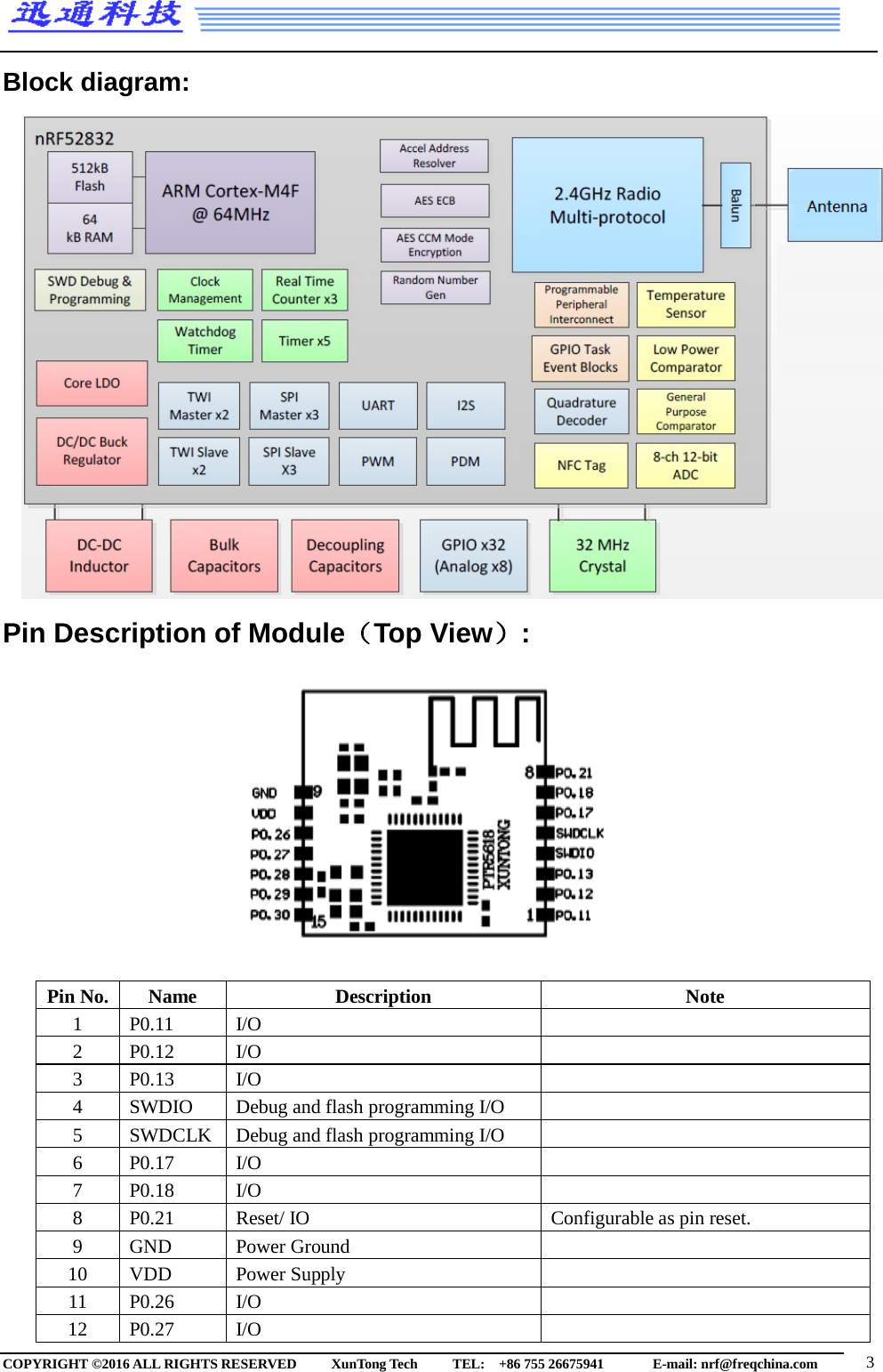
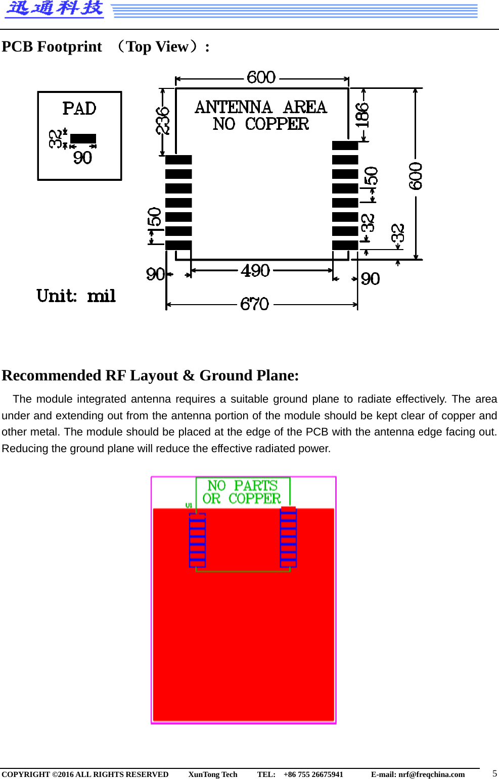
![13 P0.28 I/O ADC IN 14 P0.29 I/O ADC IN 15 P0.30 I/O ADC IN Note: An internal 4.7μF bulk capacitor has been included on the module. For those application that with heavy GPIO usage and/or current draw, it is good design practice to add additional bulk capacitance as required for your application. General Purpose I/O: The general purpose I/O is organized as one port enabling access and control of the 32 available GPIO pins through one port. Each GPIO can be accessed individually with the following user configurable features: Input/output direction Output drive strength Internal pull-up and pull-down resistors Wake-up from high or low level triggers on all pins Trigger interrupt on all pins All pins can be used by the PPI task/event system; the maximum number of pins that can be interfaced through the PPI at the same time is limited by the number of GPIOTE channels All pins can be individually configured to carry serial interface or quadrature demodulator signals Hardware RESET: There is on-chip power-on reset circuitry, But can still be used in external reset mode, in this case, GPIO pin P0.21 as an external hardware reset pin(Active Low). In order to utilize P0.21 as a hardware reset, the UICR registers PSELRESET[0] and PSELRESET[1] must be set alike, to the value of 0x7FFFFF15. When P0.21 is programmed as RESET, the internal pull-up is automatically enabled. HW debug and flash programming of Module : The Module support the two pin Serial Wire Debug (SWD) interface and offers flexible and powerful mechanism for non-intrusive debugging of program code. Breakpoints, single stepping, and instruction trace capture of code execution flow are part of this support. Pin Flash Program interface SWDIO Debug and flash programming I/O SWCLK Debug and flash programming I/O This is the hardware debug and flash programming of module, J-Link Lite support, please refer www.segger.com. COPYRIGHT ©2016 ALL RIGHTS RESERVED XunTong Tech TEL: +86 755 26675941 E-mail: nrf@freqchina.com 4](https://usermanual.wiki/LANKE-XUNTONG-TECHNOLOGY/PTR5618.User-Manual/User-Guide-3201327-Page-4.png)