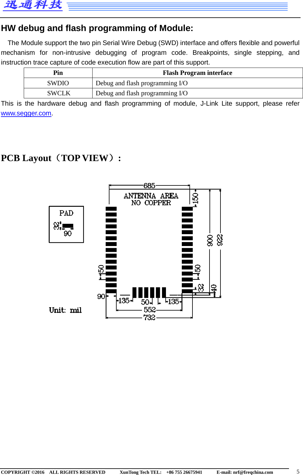
LANKE XUNTONG TECHNOLOGY PTR9018 Bluetooth low energy 4.0 modules User Manual

LANKE XUNTONG TECHNOLOGY CO.,LTD Bluetooth low energy 4.0 modules Users Manual

Contents

User Manual

   Bluetooth Low Energy System on Module   Embedded Cortex™  M0 32 bit processor  The PTR9018 ultra-low power Bluetooth Low Energy/2.4GHz Proprietary Multi-protocol modules based on the nRF51822 from Nordic Semiconductor. The module with an ARM® Cortex™ M0  32 bit processor, embedded 2.4GHz transceiver, and integrated antenna, provide a complete solution with no additional RF design, allowing faster time to market, while simplifying designs, reducing BOM costs, also reduce the burden of Regulatory approvals to enter the world market. Making you more quickly into the bluetooth smart application and remove the worries.  Features  System on Module(SOM) base on Nordic nRF51822  Bluetooth Low Energy/2.4GHz Proprietary Multi-protocol support  Complete Bluetooth Low Energy stack/profiles solution (Bluetooth 4.x and Higher)  ARM® Cortex™-M0 32 bit processor, 256 kB flash memory, 16 kB RAM    2.4 GHz transceiver,   Max TX Power +4 dBm,    -93 dBm sensitivity@BLE  31 General Purpose I/O, Configurable mapping Pins, Simple layout of external application  Internal RC Oscillator 32.768 kHz(± 250 ppm).      Flexible real-time counter and Two 16 bit and one 24 bit timers with counter mode    AES Coprocessor, Random Number Generator ,Watchdog Timer ,Temperature sensor  Rich set of Peripheral: ADC, SPI, 2-wire , and UART. Programmable Peripheral Interconnect(PPI)  Internal RC Oscillator 32.768 kHz(±  250 ppm).      Small size about 22.7mmx17.5mm x1.6mm with Antenna.              PTR9018 COPYRIGHT ©2016   ALL RIGHTS RESERVED      XunTong Tech TEL:  +86 755 26675941      E-mail: nrf@freqchina.com  1
 Typical Applications:   - 2.4 GHz Bluetooth low energy systems   - Proprietary 2.4 GHz systems   - Sports and leisure equipment   - Mobile phone accessories   - Health Care and Medical   - Consumer Electronics, Game pads   - Human Interface Devices, Remote control   - Building environment control / monitoring   - RFID, Security Applications     - Bluetooth Low Energy GateWay     - iBeacons™, Eddystone™, Indoor navigation   - Low-Power Sensors   - Connected Appliances   - Lighting Products   - Fitness devices   - Wearables  Quick Specifications:   Bluetooth Version Bluetooth 4.x and Higher Security AES-128 Radio Frequency 2.402GHz to 2.480 GHz Modulations GFSK at 250Kbps,1 Mbps, 2 Mbps data rates Transmit power -4dBm~4dBm Receiver sensitivity -93 dBm (BLE mode) Antenna On board Current Consumption TX @ -4dBm~4 dBm    ~16 mA RX only @ 1 Mbps    ~13 mA MCU running @16MHz code from Flash ~4.4 mA MCU running @16MHz code from RAM  ~2.4 mA SYSTEM ON   ~2.3 uA SYSTEM OFF   ~420 nA Operating conditions Power supply 1.9~3.6V Operating temperature  -25~+85 °C   COPYRIGHT ©2016   ALL RIGHTS RESERVED      XunTong Tech TEL:  +86 755 26675941      E-mail: nrf@freqchina.com  2
 Pin Description(Top View):               Pin  Name    Description Note Pin1  P0.20    Digital I/O   Pin2  P0.19    Digital I/O   Pin3  P0.18    Digital I/O   Pin4 P0.17  Digital I/O  Pin5 SWCLK  HW debug and flash programming I/O  Pin6 SWDIO  HW debug and flash programming I/O  Pin7 P0.16    Digital I/O  Pin8  P0.15    Digital I/O   Pin9  P0.14    Digital I/O   Pin10  P0.13    Digital I/O   Pin11  P0.12    Digital I/O   Pin12  P0.11    Digital I/O   Pin13  P0.10    Digital I/O   Pin14 P0.09  Digital I/O  Pin15  P0.08    Digital I/O   Pin16  P0.07    Digital I/O   Pin17 P0.06  Digital I/O  Pin18  P0.05    Digital I/O   Pin19  P0.04    Digital I/O   Pin20  P0.03    Digital I/O   Pin21  P0.02    Digital I/O   Pin22  P0.01    Digital I/O   Pin23  P0.00    Digital I/O   Pin24 P0.30  Digital I/O  Pin25  P0.29    Digital I/O   Pin26 P0.28  Digital I/O  Pin27 P0.27    Digital I/O  COPYRIGHT ©2016   ALL RIGHTS RESERVED      XunTong Tech TEL:  +86 755 26675941      E-mail: nrf@freqchina.com  3
 Pin28 P0.26  Digital I/O  Pin29  P0.25    Digital I/O   Pin30 P0.24  Digital I/O  Pin31 P0.23  Digital I/O  Pin32  P0.22    Digital I/O   Pin33  P0.21    Digital I/O   Pin34  VCC    Power Supply   Pin35  NC       Pin36  GND    Ground    Block diagram:                   General Purpose I/O: The general purpose I/O is organized as one port enabling access and control of the 32 available GPIO pins through one port. Each GPIO can be accessed individually with the following user configurable features:  Input/output direction  Output drive strength  Internal pull-up and pull-down resistors  Wake-up from high or low level triggers on all pins  Trigger interrupt on all pins  All pins can be used by the PPI task/event system; the maximum number of pins that can be interfaced through the PPI at the same time is limited by the number of GPIOTE channels  All pins can be individually configured to carry serial interface or quadrature demodulator signals   COPYRIGHT ©2016   ALL RIGHTS RESERVED      XunTong Tech TEL:  +86 755 26675941      E-mail: nrf@freqchina.com  4
 HW debug and flash programming of Module: The Module support the two pin Serial Wire Debug (SWD) interface and offers flexible and powerful mechanism for non-intrusive debugging of program code. Breakpoints, single stepping, and instruction trace capture of code execution flow are part of this support.  Pin Flash Program interface SWDIO Debug and flash programming I/O SWCLK Debug and flash programming I/O This is the hardware debug and flash programming of module, J-Link Lite support, please refer www.segger.com.    PCB Layout(TOP VIEW):                               COPYRIGHT ©2016   ALL RIGHTS RESERVED      XunTong Tech TEL:  +86 755 26675941      E-mail: nrf@freqchina.com  5
 Recommended RF Layout & Ground Plane: The module integrated antenna requires a suitable ground plane to radiate effectively. The area under and extending out from the antenna portion of the module should be kept clear of copper and other metal. The module should be placed at the edge of the PCB with the antenna edge facing out. Reducing the ground plane will reduce the effective radiated power.               Ordering Information:   Part Number Description PTR9018 Bluetooth Low Energy System on Module PTR9018-EVB Evaluation boards for module,with key, LED, I/O extend,sock for coin cell battery.  Absolute Maximum Ratings:   Symbol Parameter Min. Max. Unit VCC_MAX   Voltage on supply pin -0.3   3.9   V VIO_MAX   Voltage on GPIO pins (VCC > 3.6V)   -0.3   3.9   V VIO_MAX   Voltage on GPIO pins (VCC ≤ 3.6V)   -0.3   VCC + 0.3V   V TS   Storage Temperature Range   -40   125 °C    Important Notice:  Reserves the right to make corrections, modifications, and/or improvements to the product and/or its specifications at any time without notice.  Assumes no liability for the user’s product and/or applications.  Products are not authorized for use in safety-critical applications, including but not limited to life-support applications.  ATTENTION! Electrostatic Sensitive Device Observe Precaution for handling. COPYRIGHT ©2016   ALL RIGHTS RESERVED      XunTong Tech TEL:  +86 755 26675941      E-mail: nrf@freqchina.com  6

Navigation menu