LB Technology 51402TR LBA 7130RF User Manual Title
LB Technology Co., Ltd. LBA 7130RF Title
UserManual.wiki
>
LB Technology
>
51402TR User Manual
User manual
Navigation menu
Upload a User Manual
Namespaces
Wiki Guide
HTML
PDF
Info
Views
User Manual
Discussion / Help
Navigation
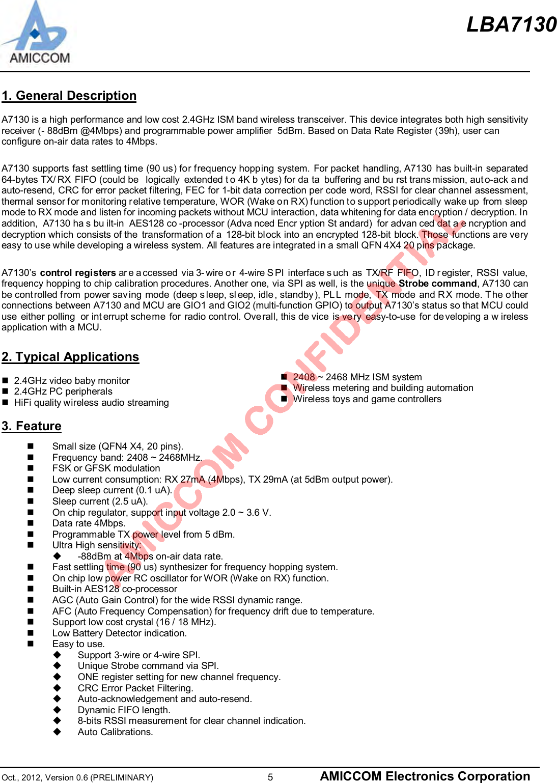
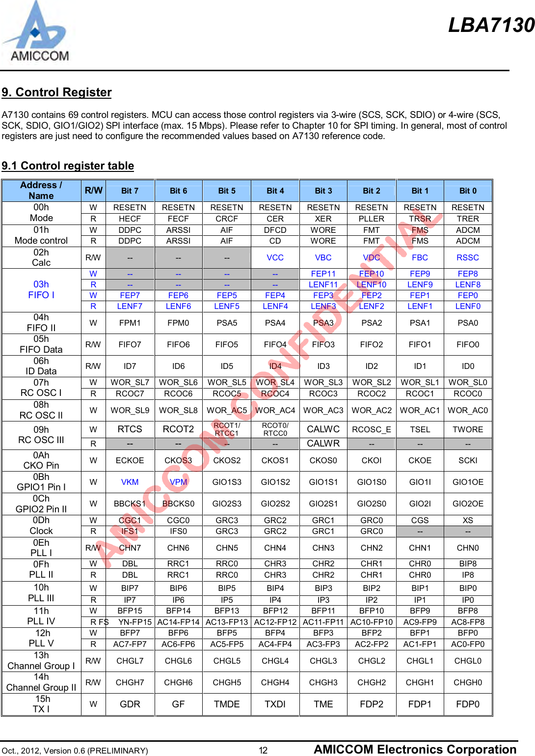
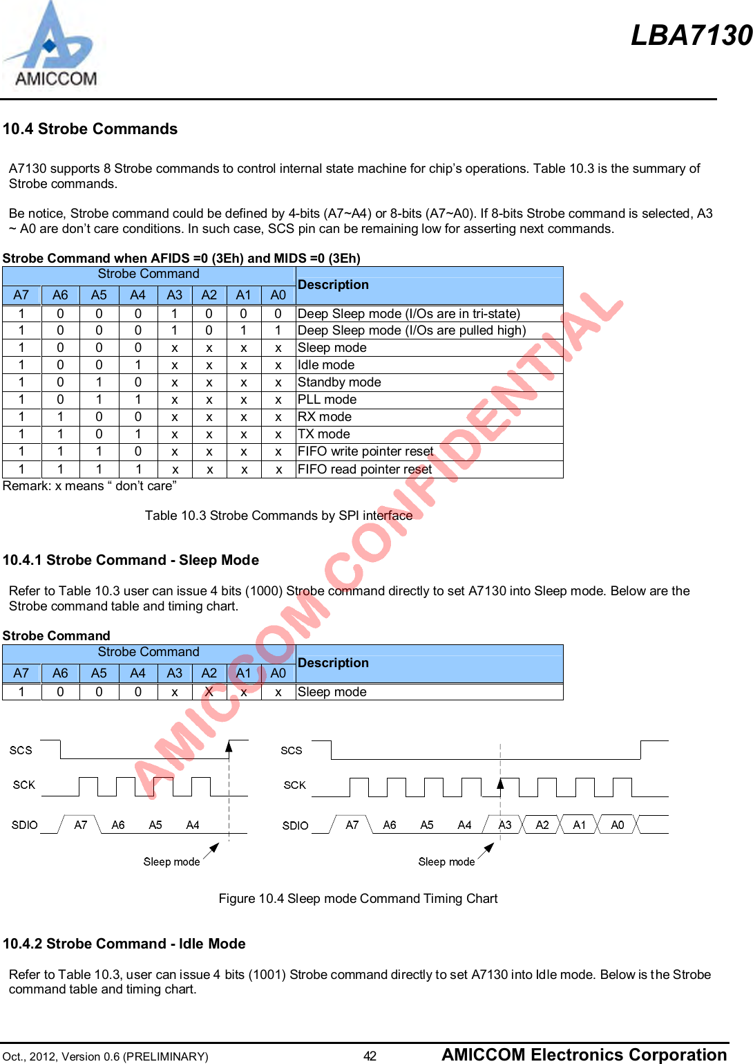
![LBA7130Oct., 2012, Version 0.6 (PRELIMINARY) 2 AMICCOM Electronics CorporationTable of Contents1. General Description....................................................................................................................................................... 52. Typical Applications ....................................................................................................................................................... 53. Feature ......................................................................................................................................................................... 54. Pin Configurations ......................................................................................................................................................... 65. Pin Description (I: input; O: output, I/O: input or output)................................................................................................... 76. Chip Block Diagram....................................................................................................................................................... 87. Absolute Maximum Ratings............................................................................................................................................ 98. Electrical Specification..................................................................................................................................................109. Control Register ...........................................................................................................................................................129.1 Control register table............................................................................................................................................129.2 Control register description ..................................................................................................................................159.2.1 Mode Register (Address: 00h)....................................................................................................................159.2.2 Mode Control Register (Address: 01h)......................................................................................................159.2.3 Calibration Control Register (Address: 02h)..............................................................................................169.2.4 FIFO Register I (Address: 03h).................................................................................................................169.2.5 FIFO Register II (Address: 04h)................................................................................................................169.2.6 FIFO DATA Register (Address: 05h) .........................................................................................................169.2.7 ID DATA Register (Address: 06h)................................................................................................................169.2.8 RC OSC Register I (Address: 07h) .............................................................................................................179.2.9 RC OSC Register II (Address: 08h).............................................................................................................179.2.10 RC OSC Register III (Address: 09h)..........................................................................................................179.2.11 CKO Pin Control Register (Address: 0Ah) .................................................................................................179.2.12 GIO1 Pin Control Register I (Address: 0Bh)...............................................................................................189.2.13 GIO2 Pin Control Register II (Address: 0Ch) .............................................................................................209.2.14 Clock Register (Address: 0Dh)..................................................................................................................219.2.15 PLL Register I (Address: 0Eh)...................................................................................................................219.2.16 PLL Register II (Address: 0Fh)..................................................................................................................219.2.17 PLL Register III (Address: 10h).................................................................................................................229.2.18 PLL Register IV (Address: 11h).................................................................................................................229.2.19 PLL Register V (Address: 12h) ...............................................................................................................229.2.20 Channel Group Register I (Address: 13h)..................................................................................................229.2.21 Channel Group Register II (Address: 14h).................................................................................................229.2.22 TX Register I (Address: 15h).....................................................................................................................239.2.23 TX Register II (Address: 16h)....................................................................................................................239.2.24 Delay Register I (Address: 17h)................................................................................................................239.2.25 Delay Register II (Address: 18h) ...............................................................................................................249.2.26 RX Register (Address: 19h)......................................................................................................................249.2.27 RX Gain Register I (Address: 1Ah)............................................................................................................259.2.28 RX Gain Register II (Address: 1Bh)...........................................................................................................259.2.29 RX Gain Register III (Address: 1Ch) .........................................................................................................259.2.30 RX Gain Register IV (Address: 1Dh).........................................................................................................269.2.31 RSSI Threshold Register (Address: 1Eh) ..................................................................................................269.2.32 ADC Control Register (Address: 1Fh)........................................................................................................269.2.33 Code Register I (Address: 20h).................................................................................................................269.2.34 Code Register II (Address: 21h)................................................................................................................279.2.35 Code Register III (Address: 22h)...............................................................................................................279.2.36 IF Calibration Register I (Address: 23h).....................................................................................................279.2.37 IF Calibration Register II (Address: 24h)....................................................................................................289.2.38 VCO current Calibration Register (Address: 25h).......................................................................................289.2.39 VCO band Calibration Register I (Address: 26h)........................................................................................289.2.40 VCO band Calibration Register II (Address: 27h).......................................................................................299.2.41 VCO Deviation Calibration Register I (Address: 28h) .................................................................................299.2.42 VCO Deviation Calibration Register II (Address: 29h) ................................................................................299.2.43 DASP0 (Address: 2Ah, Page 0 by AGT [3:0]=0) ........................................................................................309.2.43 DASP1 (Address: 2Ah, Page 1 by AGT[3:0]=1) .........................................................................................30](https://usermanual.wiki/LB-Technology/51402TR/User-Guide-1922627-Page-2.png)
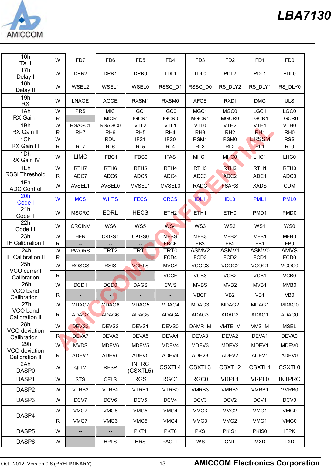
![LBA7130Oct., 2012, Version 0.6 (PRELIMINARY) 3 AMICCOM Electronics Corporation9.2.43 DASP2 (Address: 2Ah, Page 2 by AGT[3:0]=2) .........................................................................................309.2.43 DASP3 (Address: 2Ah, Page 3 by AGT[3:0]=3) .........................................................................................319.2.43 DASP4 (Address: 2Ah, Page 4 by AGT[3:0]=4) .........................................................................................319.2.43 DASP5 (Address: 2Ah, Page 5 by AGT[3:0]=5) .........................................................................................319.2.43 DASP6 (Address: 2Ah, Page 6 by AGT[3:0]=6) .........................................................................................319.2.43 DASP7 (Address: 2Ah, Page 7 by AGT[3:0]=7) .........................................................................................319.2.44 VCO Modulation Delay Register (Address: 2Bh)........................................................................................319.2.45 Battery detect Register (Address: 2Ch).....................................................................................................329.2.46 TX test Register (Address: 2Dh) ...............................................................................................................329.2.47 Rx DEM test Register I (Address: 2Eh) .....................................................................................................329.2.48 Rx DEM test Register II (Address: 2Fh).....................................................................................................339.2.49 Charge Pump Current Register I (Address: 30h) .......................................................................................339.2.50 Charge Pump Current Register II (Address: 31h).......................................................................................339.2.51 Crystal test Register (Address: 32h)..........................................................................................................339.2.52 PLL test Register (Address:33h) ...............................................................................................................349.2.53 VCO test Register I (Address:34h)............................................................................................................349.2.54 RF Analog Test Register (Address: 35h)....................................................................................................349.2.55 AES Key data Register (Address: 36h)......................................................................................................359.2.56 Channel Select Register (Address: 37h)....................................................................................................359.2.57 ROMP0 (Address: 38h, Page 0 by AGT[3:0]=0).........................................................................................359.2.57 ROMP1 (Address: 38h, Page 1 by AGT[3:0]=1).........................................................................................359.2.57 ROMP2 (Address: 38h, Page 2 by AGT[3:0]=2).........................................................................................369.2.57 ROMP3 (Address: 38h, Page 3 by AGT[3:0]=3).........................................................................................369.2.57 ROMP4 (Address: 38h, Page 4 by AGT[3:0]=4).........................................................................................369.2.58 Data Rate Clock Register (Address: 39h)..................................................................................................369.2.59 FCR Register (Address: 3Ah) ...................................................................................................................369.2.60 ARD Register (Address: 3Bh) ...................................................................................................................379.2.61 AFEP Register (Address: 3Ch)..................................................................................................................379.2.62 FCB Register (Address: 3Dh) ...................................................................................................................379.2.63 KEYC Register (Address: 3Eh).................................................................................................................389.2.64 USID Register (Address: 3Fh) ..................................................................................................................3810. SPI.............................................................................................................................................................................3910.1 SPI Format ........................................................................................................................................................4010.2 SPI Timing Characteristic ...................................................................................................................................4010.3 SPI Timing Chart................................................................................................................................................4110.3.1 Timing Chart of 3-wire SPI........................................................................................................................4110.3.2 Timing Chart of 4-wire SPI........................................................................................................................4110.4 Strobe Commands .............................................................................................................................................4210.4.1 Strobe Command - Sleep Mode................................................................................................................4210.4.2 Strobe Command - ldle Mode ...................................................................................................................4210.4.3 Strobe Command - Standby Mode ............................................................................................................4310.4.4 Strobe Command - PLL Mode...................................................................................................................4310.4.5 Strobe Command - RX Mode....................................................................................................................4410.4.6 Strobe Command - TX Mode ....................................................................................................................4410.4.7 Strobe Command – FIFO Write Pointer Reset ...........................................................................................4410.4.8 Strobe Command – FIFO Read Pointer Reset ...........................................................................................4510.4.9 Strobe Command – Deep Sleep Mode......................................................................................................4510.5 Reset Command................................................................................................................................................4610.6 ID Accessing Command.....................................................................................................................................4610.6.1 ID Write Command...................................................................................................................................4610.6.2 ID Read Command ..................................................................................................................................4710.7 FIFO Accessing Command.................................................................................................................................4710.7.1 TX FIFO Write Command.........................................................................................................................4710.7.2 Rx FIFO Read Command.........................................................................................................................4811. State machine.............................................................................................................................................................4911.1 Key states..........................................................................................................................................................4911.2 FIFO mode ........................................................................................................................................................5011.3 Direct mode .......................................................................................................................................................5112. Crystal Oscillator ........................................................................................................................................................5412.1 Use External Crystal ..........................................................................................................................................54](https://usermanual.wiki/LB-Technology/51402TR/User-Guide-1922627-Page-3.png)
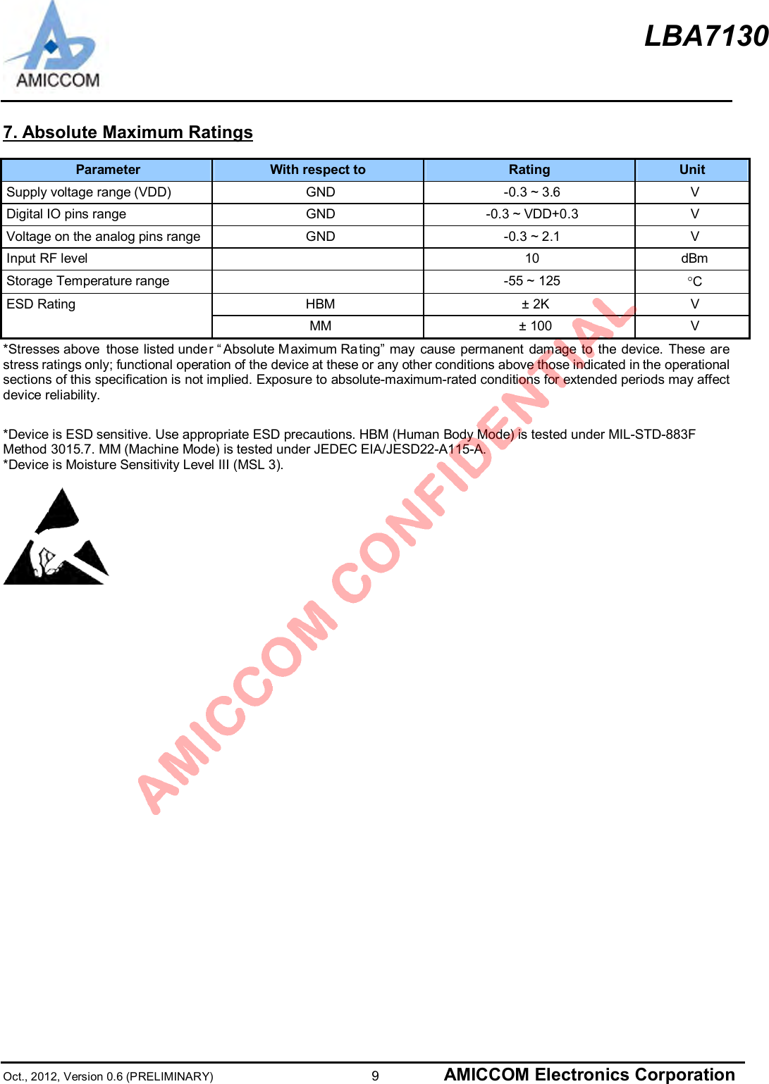
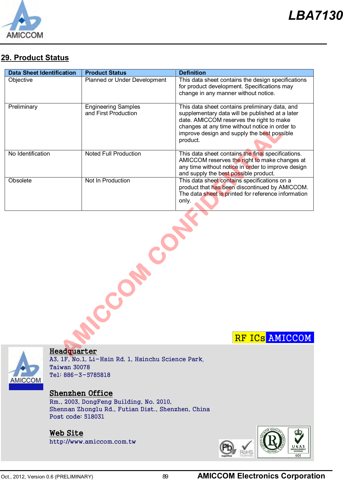
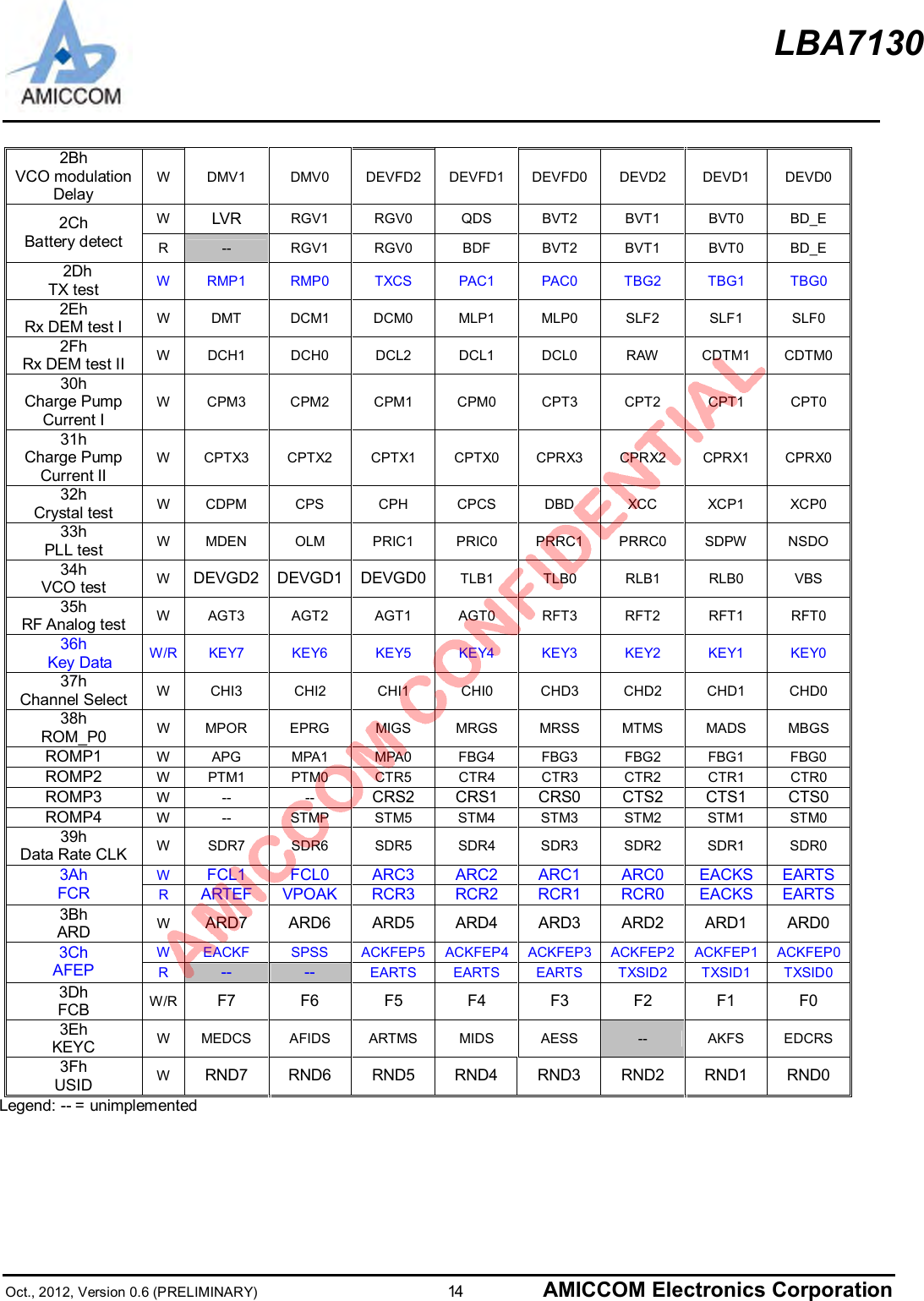
![LBA7130Oct., 2012, Version 0.6 (PRELIMINARY) 11 AMICCOM Electronics CorporationIF Filter bandwidth IFS = [11], 4Mbps 4.8M HzIF center frequency IFS = [11], 4Mbps 4M HzCo-Channel (C/I0) 11 dB±4MHz Adjacent Channel 0 dB±8MHz Adjacent Channel - 10 dB±12MHz Adjacent Channel - 20 dB±16MHz Adjacent Channel - 30 dBInterference *7(4Mbps , IF = 4MHz)Image (C/IIM)- 10 dBMaximum Operating Input Power @RF input (BER=0.1%) 5 dBm30MHz~1GHz -57 dBmRX Spurious Emission *41GHz~12.75GHz -47AGC = 0 -95 -50 dBmRSSI RangeAGC = 1 -95 -20 dBmRX Ready Time 80 msRegulatorRegulator settling time Pin 2 connected to 470pF.(Sleep to idle).0.5 msBand-gap reference voltage 1.28 VRegulator output voltage 1.79 1.8 2.3 VDigital IO DC characteristicsHigh Level Input Voltage (VIH)0.8*VDD VDD VLow Level Input Voltage (VIL) 0 0.2*VDD VHigh Level Output Voltage (VOH)@IOH= -0.5mA VDD-0.4 VDD VLow Level Output Voltage (VOL)@IOL= 0.5mA 0 0.4 VNote 1: When digital I/O pins are configured as input, those pins shall NOT be floating but pull either high or low (SCS shall be pulled high only); otherwise, leakage current will be induced.Note 2: Xtal settling time is depend on Xtal package type, Xtal ESR and Xtal Cm.Note 3: Refer to Delay Register I (17h) to set PDL (PLL settling delay).Note 4: With external RF filter that provides minimum 17dB of attenuation in the band: 30MHz ~ 2GHz and 3GHz ~12.75GHz.Note 5: Refer to TX Register II (16h) to set FD [7:0].Note 6: Refer to Delay Register I (17h) to set PDL and TDL.Note 7: The wanted signal is set above sensitivity level +3dB. The modulation data of wanted signal and interferer are PN9 and PN15, respectively.](https://usermanual.wiki/LB-Technology/51402TR/User-Guide-1922627-Page-11.png)
![LBA7130Oct., 2012, Version 0.6 (PRELIMINARY) 15 AMICCOM Electronics Corporation9.2 Control register description9.2.1 Mode Register (Address: 00h)Name R/W Bit 7 Bit 6 Bit 5 Bit 4 Bit 3 Bit 2 Bit 1 Bit 0RHECF FECF CRCF CER XER PLLER TRSR TRERMode WRESETN RESETN RESETN RESETN RESETN RESETN RESETN RESETNRESETN: Write to this register by 0x00 to issue reset command, then it is auto clearHECF: Head Control Flag. (HECF will be clear after issue a strobe command.)HEC is CRC-8 result for the optional Packet Header (Please refer to chapter 16 for details)[0]: HEC pass. [1]: HEC error.FECF: FEC flag. (FECF will be clear after issue any strobe command.)[0]: FEC pass. [1]: FEC error.CRCF: CRC flag. (CRCF will be clear after issue any strobe command.)[0]: CRC pass. [1]: CRC error.CER: RF chip enable status.[0]: RF chip is disabled. [1]: RF chip is enabled.XER: Internal crystal oscillator enabled status.[0]: Crystal oscillator is disabled. [1]: Crystal oscillator is enabled.PLLE: PLL enabled status.[0]: PLL is disabled. [1]: PLL is enabled.TRER: TRX state enabled status.[0]: TRX is disabled. [1]: TRX is enabled.TRSR: TRX Status Register.[0]: RX state. [1]: TX state.Serviceable if TRER=1 (TRX is enable).9.2.2 Mode Control Register (Address: 01h)Name R/W Bit 7 Bit 6 Bit 5 Bit 4 Bit 3 Bit 2 Bit 1 Bit 0RDDPC ARSSI AIF DFCD WORE FMT FMS ADCMMode Control I WDDPC ARSSI AIF CD WORE FMT FMS ADCMDDPC (Direct mode data pin control): Direct mode modem data can be accessed via SDIO pin.[0]: Disable. [1]: Enable.ARSSI: Auto RSSI measurement while entering RX mode.[0]: Disable. [1]: Enable.AIF (Auto IF Offset): RF LO frequency will auto offset one IF frequency while entering RX mode.[0]: Disable. [1]: Enable.CD: Carrier detector (Read only).[0]: Input power below threshold. [1]: Input power above threshold.DFCD: Data Filter by CD : The received packet would be filtered if the input power level is below RTH (1Eh).[0]: Disable. [1]: Enable.WORE: WOR (Wake On RX) Function Enable.[0]: Disable. [1]: Enable.FMT: Reserved for internal usage only. Shall be set to [0].FMS: Direct/FIFO mode select.[0]: Direct mode. [1]: FIFO mode.ADCM: ADC measurement enable (Auto clear when done).[0]: Disable measurement or measurement finished. [1]: Enable measurement.Refer to chapter 17 for details.](https://usermanual.wiki/LB-Technology/51402TR/User-Guide-1922627-Page-15.png)
![LBA7130Oct., 2012, Version 0.6 (PRELIMINARY) 16 AMICCOM Electronics Corporation9.2.3 Calibration Control Register (Address: 02h)Name R/W Bit 7 Bit 6 Bit 5 Bit 4 Bit 3 Bit 2 Bit 1 Bit 0Mode Control II R/W -- -- -- VCC VBC VDC FBC RSSCVCC: VCO Current calibration enable (Auto clear when done).[0]: Disable. [1]: Enable.VBC: VCO Bank calibration enable (Auto clear when done).[0]: Disable. [1]: Enable.VDC: VCO Deviation calibration enable (Auto clear when done).[0]: Disable. [1]: Enable.FBC: IF Filter Bank calibration enable (Auto clear when done).[0]: Disable. [1]: Enable.RSSC: RSSI calibration enable (Auto clear when done).[0]: Disable. [1]: Enable.9.2.4 FIFO Register I (Address: 03h)Name R/W Bit 15 Bit 14 Bit 13 Bit 12 Bit 11 Bit 10 Bit 9 Bit 8W-- -- -- -- FEP11 FEP10 FEP9 FEP8R-- -- -- -- LENF11 LENF10 LENF9 LENF8WFEP7 FEP6 FEP5 FEP4 FEP3 FEP2 FEP1 FEP0FIFO IRLENF7 LENF6 LENF5 LENF4 LENF3 LENF2 LENF1 LENF0FEP [11:0]: FIFO End Pointer for TX FIFO and Rx FIFO.Data Sequence is FEP[7:0] and FEP[15:8].Please refer to chapter 16 for details.LENF [11:0]: Received FIFO Length for dynamic FIFO function. (Ready Only)When EDRL =1, that means dynamic FIFO is enabled, MCU can read LENF [11:0] to know the RX FIFO length of the comingpacket. Please refer to chapter 16 for details.9.2.5 FIFO Register II (Address: 04h)Name R/W Bit 7 Bit 6 Bit 5 Bit 4 Bit 3 Bit 2 Bit 1 Bit 0FIFO II W FPM1 FPM0 PSA5 PSA4 PSA3 PSA2 PSA1 PSA0FPM [1:0]: FIFO Pointer MarginPSA [5:0]: Used for Segment FIFO.Refer to chapter 16 for details.9.2.6 FIFO DATA Register (Address: 05h)Bit R/W Bit 7 Bit 6 Bit 5 Bit 4 Bit 3 Bit 2 Bit 1 Bit 0WTX-FIFO[7:0]NameR/W RX-FIFO[7:0]FIFO [7:0]: TX FIFO / RX FIFOTX FIFO and RX FIFO share the same address (05h).TX FIFO and RX FIFO are separated physical 64 Bytes.Refer to chapter 16 for details.9.2.7 ID DATA Register (Address: 06h)Name R/W Bit 7 Bit 6 Bit 5 Bit 4 Bit 3 Bit 2 Bit 1 Bit 0ID DATA R/W ID7 ID6 ID5 ID4 ID3 ID2 ID1 ID0ID [7:0]: ID data.When this address is accessed, ID Data is input or output sequential (ID Byte 0,1, 2 and 3) corresponding to Write or Read.](https://usermanual.wiki/LB-Technology/51402TR/User-Guide-1922627-Page-16.png)
![LBA7130Oct., 2012, Version 0.6 (PRELIMINARY) 17 AMICCOM Electronics CorporationRecommend to set ID Byte 0 = 5xh or Axh.Refer to section 10.6 for details.9.2.8 RC OSC Register I (Address: 07h)Name R/W Bit 7 Bit 6 Bit 5 Bit 4 Bit 3 Bit 2 Bit 1 Bit 0RRCOC7 RCOC6 RCOC5 RCOC4 RCOC3 RCOC2 RCOC1 RCOC0RC OSC I WWOR_SL7 WOR_SL6 WOR_SL5 WOR_SL4 WOR_SL3 WOR_SL2 WOR_SL1 WOR_SL0RCOC [7:0]: Reserved for internal usage (read only).9.2.9 RC OSC Register II (Address: 08h)Name R/W Bit 7 Bit 6 Bit 5 Bit 4 Bit 3 Bit 2 Bit 1 Bit 0RC OSC II W WOR_SL9 WOR_SL8 WOR_AC5 WOR_AC4 WOR_AC3 WOR_AC2 WOR_AC1 WOR_AC0WOR_AC [5:0]: 6-bits WOR Active Timer for WOR and TWOR FunctionWOR_SL [9:0]: 10-bits WOR Sleep Timer for WOR and TWOR Function.WOR_SL [9:0] are from address (07h) and (08h),Active period = (WOR_AC+1) x (1/4092).Sleep period = (WOR_SL+1) x (1/32) x (1/4092).9.2.10 RC OSC Register III (Address: 09h)Name R/W Bit 7 Bit 6 Bit 5 Bit 4 Bit 3 Bit 2 Bit 1 Bit 0WRTCS RCO T2 RCOT1/RTCC1RCOT0/RTCC0 CALWC RCOSC_E TSEL TWORERC OSC IIIR-- -- -- -- CALWR -- -- --RTCS: internal Oscillator selection in sleep mode. Recommend RTCS= [0].[0]: RC oscillator. [1]: RTC oscillator.RCOT[2:0]: Reserved for internal used. Recommend RCOT= [000].RCOT[1:0]: RCOSC current select for RC oscillator calibration.[00]: 240nA [01]: 280nA [10]: 320nA [11]: 360nATSEL: Timer select for TWOR function.[0]: Use WOR_AC. [1]: Use WOR_SL.CALWC: RC Oscillator Calibration Enable.[0]: Disable. [1]: Enable.CALWR: RC Oscillator Calibration ending indication.[0]: ending. [1]: Not ending.RCOSC_E: RC-oscillator enable.[0]: Disable. [1]: Enable.TSEL: Timer Duty select for TWOR function.[0]: Use WOR_AC. [1]: Use WOR_SL.TWORE: Enable TWOR function.[0]: WOR mode. [1]: TWOR mode.9.2.11 CKO Pin Control Register (Address: 0Ah)Name R/W Bit 7 Bit 6 Bit 5 Bit 4 Bit 3 Bit 2 Bit 1 Bit 0CKO Pin Control W ECKOE CKOS3 CKOS2 CKOS1 CKOS0 CKOI CKOE SCKIECKOE: CKO pin Output Enable.[0]: Disable. [1]: Enable.CKOS [3:0]: CKO pin output select.](https://usermanual.wiki/LB-Technology/51402TR/User-Guide-1922627-Page-17.png)
![LBA7130Oct., 2012, Version 0.6 (PRELIMINARY) 18 AMICCOM Electronics Corporation[0000]: DCK (TX data clock) in TX mode, RCK (RX recovery clock) in RX mode.[0001]: DCK (TX data clock) in TX mode, RCK (RX recovery clock) in RX mode.[0010]: FPF (FIFO pointer flag).[0011]: EOP, EOVBC, EOFBC, EOVCC, EOVDC, RSSC_OK. (Internal usage only).[0100]: External clock output= FSYCK / 2.[0101]: External clock output / 2= FSYCK / 4.[0110]: RXD[0111]: FSYNC.[1000]: WCK.[1001]: PF8M.(8Mhz, internal usage)[1010]: ROSC.[1011]: MXDEC(SLF[0]=1:~OKADCN, SLF[1]=0: DEC , internal usage)[1100]: BDF (Battery Detect flag).[1101]: FSYCK ..[1110]: VPOAK.[1111]: WRTC (internal usage)CKOI: CKO pin output signal invert.[0]: Non-inverted output. [1]: Inverted output.CKOE: CKO pin Output Enable.[0]: High Z. [1]: Enable.SCKI: SPI clock input invert.[0]: Non-inverted input. [1]: Inverted input.9.2.12 GIO1 Pin Control Register I (Address: 0Bh)Name R/W Bit 7 Bit 6 Bit 5 Bit 4 Bit 3 Bit 2 Bit 1 Bit 0GIO1 Pin Control I W VKM VPM GIO1S3 GIO1S2 GIO1S1 GIO1S0 GIO1I GI O1OEVKM: Valid packet mode select.[0]: by event.[1]: by pulse.VPM: Valid Pulse width select.[0]: 20u. [1]: 40u.TX Mode (disable auto-resend, EAR=0).](https://usermanual.wiki/LB-Technology/51402TR/User-Guide-1922627-Page-18.png)
![LBA7130Oct., 2012, Version 0.6 (PRELIMINARY) 19 AMICCOM Electronics CorporationRX Mode (disable Auto-ack, EAK =0).Note1, If auto-resend is enabled (EAR = 1), WTR behavior is different while it is output to GIO1 and GIO2.Note2, If auto-ack is enabled (EAK = 1), WTR behavior is different while it is output to GIO1 and GIO2.Note3, VPOAK’s behavior is controlled by VPM (0Bh) and VPW (0Bh).Refer to chapter 19 for detailsGIO1S [3:0]: GIO1 pin function select.GIO1S [3:0] TX state RX state[0000] WTR (Wait until TX or RX finished)[0001] EOAC (end of access code) FSYNC (frame sync)[0010] TMEO (TX modulation enable) CD (carrier detect)[0011] Preamble Detect Output (PMDO)[0100] If RCOSC_E =1, output TWOR.If RCOSC_E =0, output CWTR signal. (internal usage)[0101] In phase demodulator input(DMII)or VT[0] (internal usage)[0110] SDO ( 4 wires SPI data out)[0111] TRXD In/Out (Direct mode)[1000] RXD (Direct mode)[1001] TXD (Direct mode)[1010] PDN_RX[1011] External FSYNC input in RX direct mode (internal usage)[1100] MXINC(SLF[0]=1:EOADC.SLF[1]=0:INC.) (internal usage)[1101] FPF[1110] VPOAK (Valid Packet or Auto ACK OK Output)[1111] FMTDO (internal usage)If GIO1S = [0100] and RCOSC_E = 0, CWTR is an internal signal to monitor TX/RX cycles of auto-ack and auto-resend.IfGIO1S = [1011] and direct mode is selected, the internal frame sync function will be disabled. In such case, A7130 supportsto accept an external frame sync signal from MCU to feed to GIO1 pin to determine the timing of fixing DC estimation voltageof demodulator.GIO1I: GIO1 pin output signal invert.[0]: Non-inverted output. [1]: Inverted output.GIO1OE: GIO1pin output enable.[0]: High Z. [1]: Enable.](https://usermanual.wiki/LB-Technology/51402TR/User-Guide-1922627-Page-19.png)
![LBA7130Oct., 2012, Version 0.6 (PRELIMINARY) 20 AMICCOM Electronics Corporation9.2.13 GIO2 Pin Control Register II (Address: 0Ch)Name R/W Bit 7 Bit 6 Bit 5 Bit 4 Bit 3 Bit 2 Bit 1 Bit 0GIO2 Pin Control II W BBCKS1 BBCKS0 GIO2S3 GIO2S2 GIO2S1 GIO2S0 GIO2I GI O2OEBBCKS [1:0]: Clock select for digital block. Recommend BBCKS = [00].[00]: FSYCK.[01]: FSYCK / 2. [10]: FSYCK / 4. [11]: FSYCK / 8.GIO2S [3:0]: GIO2 pin function select.GIO2S TX state RX state[0000] WTR (Wait until TX or RX finished)[0001] EOAC (end of access code) FSYNC (frame sync)[0010] TMEO (TX modulation enable) CD (carrier detect)[0011] Preamble Detect Output (PMDO)[0100] If RCOSC_E =1, output TWOR.If RCOSC_E =0, output CWTR signal. (internal usage)[0101] Quadrature phase demodulator input (DMIQ) (internal usage)[0110] SDO (4 wires SPI data out)[0111] TRXD In/Out (Direct mode)[1000] RXD (Direct mode)[1001] TXD (Direct mode)[1010] PDN_TX[1011] ROMOK(ROM Program OK) (internal usage)[1100] BDF (Battery Detect Flag)[1101] FPF[1110] VPOAK (Valid Packet or Auto ACK OK Output)[1111] DCK (internal usage)If GIO2S = [0100] and RCOSC_E = 0, CWTR is an internal signal to monitor TX/RX cycles of auto-ack and auto-resend.GIO2I: GIO2 pin output signal invert.[0]: Non-inverted output. [1]: Inverted output.GIO2OE: GIO2 pin Output Enable.[0]: High Z. [1]: Enable.In TX modeSPI(SCS,SCK,SDIO)T1No Command RequiredT2GIO1 Pin - WTR(GIO1S[3:0]=0000)10 us + (PDL+TDL)Next InstructionPreamble + ID Code + PayloadRF PortAuto BackPLL Mode + CRCT3PLL ModeGIO2 Pin - TMEO(GIO2S[3:0]=0010)T016 us PA Ramp Down< 1usTX-Strobe(Output)In RX mode](https://usermanual.wiki/LB-Technology/51402TR/User-Guide-1922627-Page-20.png)
![LBA7130Oct., 2012, Version 0.6 (PRELIMINARY) 21 AMICCOM Electronics CorporationSPI(SCS,SCK,SDIO)T1No Command RequiredT2GIO1 Pin - WTR(GIO1S[3:0]=0000)10us+PDL+TDLNext InstructionPreamble + ID Code + PayloadRF PortAuto BackPLL Mode + CRCPLL ModeGIO2 Pin - FSYNC(GIO2S[3:0]=0001)T0< 1usRX-Strobe(Input)ID-Matched9.2.14 Clock Register (Address: 0Dh)Name R/W Bit 7 Bit 6 Bit 5 Bit 4 Bit 3 Bit 2 Bit 1 Bit 0Clock W CGC1 CGC0 GRC3 GRC2 GRC1 GRC0 CGS XSRIFS1 IFS0 GRC3 GRC2 GRC1 GRC0 -- --CGC [1:0]: Clock Gen. Current select. Shall be set to [10].GRC [3:0]: Clock generation reference counter. Recommend GRC = [0111] for 16MHz Xtal.GRC [3:0] is used to let below formula be true when CGS = 1.FXTAL x (DBL+1) / (GRC+1) = 2MHz.CGS: Clock generator enable. Recommend CGS = [1][0]: Disable. [1]: Enable.XS: Crystal oscillator select. Recommend XS = [1][0]: External clock. [1]: Crystal.IFS [1:0]: IF band selection. (Ready only)9.2.15 PLL Register I (Address: 0Eh)Name R/W Bit 7 Bit 6 Bit 5 Bit 4 Bit 3 Bit 2 Bit 1 Bit 0PLL I R/W CHN7 CHN6 CHN5 CHN4 CHN3 CHN2 CHN1 CHN0CHN [7:0]: LO channel number select.Refer to chapter 14 for details.9.2.16 PLL Register II (Address: 0Fh)Name R/W Bit 7 Bit 6 Bit 5 Bit 4 Bit 3 Bit 2 Bit 1 Bit 0RDBL RRC1 RRC0 CHR3 CHR2 CHR1 CHR0 IP8PLL II WDBL RRC1 RRC0 CHR3 CHR2 CHR1 CHR0 BIP8DBL: Crystal frequency doublers selection.[0]: Disable. FXREF = FXTAL.[1]: Enable. FXREF =2 * FXTAL.In FIFO mode, recommend to set DBL =0.In Direct mode, recommend to set DBL =1.Please refer to A7130 reference code for details.RRC [1:0]: RF PLL reference counter setting. Recommend RRC = [00].The PLL com parison frequency, FPFD = FCRYSTAL *(DBL+1) / (RRC+1).](https://usermanual.wiki/LB-Technology/51402TR/User-Guide-1922627-Page-21.png)
![LBA7130Oct., 2012, Version 0.6 (PRELIMINARY) 22 AMICCOM Electronics CorporationCHR [3:0]: PLL channel step setting.In FIFO mode, recommend to set CHR [3:0] = [0111].In Direct mode, recommend to set CHR [3:0] = [1111].Please refer to chapter 14 and A7130 reference code for details.9.2.17 PLL Register III (Address: 10h)Name R/W Bit 7 Bit 6 Bit 5 Bit 4 Bit 3 Bit 2 Bit 1 Bit 0RIP7 IP6 IP5 IP4 IP3 IP2 IP1 IP0PLL III WBIP7 BIP6 BIP5 BIP4 BIP3 BIP2 BIP1 BIP0BIP [8:0]: LO base frequency integer part setting. (0Fh and 10h)In FIFO mode, recommend to set BIP [8:0] = [0x096].In Direct mode, recommend to set BIP [8:0] = [0x04B].Please refer to chapter 14 and A7130 reference code for details.IP [8:0]: LO frequency integer part value.IP [8:0] are from address (0Fh) and (10h),Refer to chapter 14 for details.9.2.18 PLL Register IV (Address: 11h)Name R/W Bit 7 Bit 6 Bit 5 Bit 4 Bit 3 Bit 2 Bit 1 Bit 0RRAC15 RAC14 RAC13 RAC12 RAC11 RAC10 RAC9 RAC8PLL IV WBFP15 BF P14 BFP13 BFP12 BF P11 BFP10 BFP9 BFP89.2.19 PLL Register V (Address: 12h)Name R/W Bit 7 Bit 6 Bit 5 Bit 4 Bit 3 Bit 2 Bit 1 Bit 0RRAC7 RAC6 RAC5 RAC4 RAC3 RAC2 RAC1 RAC0PLL V WBFP7 BFP6 BFP5 BFP4 BFP3 BFP2 BFP1 BFP0BFP [15:0]: LO base frequency fractional part setting. (11h and 12h)In FIFO mode, recommend to set BFP [15:0] = [0x0004].In Direct mode, recommend to set BFP [15:0] = [0x0002].Please refer to chapter 14 and A7130 reference code for details.RAC [15:0]: Auto Frequency compensation value if AFC (19h) =1.RAC [15:0] NoteAFC = 1 PLLFF [15:0] LO Freq. compensation valueAFC = 0 {SYNCF, AC [14:0]}9.2.20 Channel Group Register I (Address: 13h)Name R/W Bit 7 Bit 6 Bit 5 Bit 4 Bit 3 Bit 2 Bit 1 Bit 0CHGI R/W CHGL7 CHGL6 CHGL5 CHGL4 CHGL3 CHGL2 CHGL1 CHGL0CHGL [7:0]: PLL channel group low boundary setting for auto-calibration. Recommed CHGL[7:0] = 0x3C.Refer to A7130 reference code for details.9.2.21 Channel Group Register II (Address: 14h)Name R/W Bit 7 Bit 6 Bit 5 Bit 4 Bit 3 Bit 2 Bit 1 Bit 0CHGII R/W CHGH7 CHGH6 CHGH5 CHGH4 CHGH3 CHGH2 CHGH1 CHGH0CHGH [7:0]: PLL channel group high boundary setting for auto-calibration. Recommed CHGH[7:0] = 0x78.Refer to A7130 reference code for details.PLL calibration frequency is divided into 3 groups by CHGL and CHGH:ChannelGroup1 0 ~ CHGL-1Group2 CHGL ~ CHGH-1](https://usermanual.wiki/LB-Technology/51402TR/User-Guide-1922627-Page-22.png)
![LBA7130Oct., 2012, Version 0.6 (PRELIMINARY) 23 AMICCOM Electronics CorporationGroup3 CHGH ~ 2559.2.22 TX Register I (Address: 15h)Name R/W Bit 7 Bit 6 Bit 5 Bit 4 Bit 3 Bit 2 Bit 1 Bit 0TX I W GDR GF TMDE TXDI TME FDP2 FDP1 FDP0GDR: Gaussian Filter Over Sampling Rate Select. Recommend GDR = [1].[0]: BT= 0.7 [1]: BT= 0.5GF: Gaussian Filter Select.[0]: Disable. [1]: Enable.TMDE: TX modulation enable for VCO modulation. Recommend TMDE = [1].[0]: Disable. [1]: Enable.TXDI: TX data invert. Recommend TXDI = [0].[0]: Non-invert. [1]: Invert.TME: TX modulation enable. Recommend TME = [1].[0]: Disable. [1]: Enable.FDP [2:0]: Frequency deviation power setting. Recommend FDP = [110].In FIFO mode, recommend to set FDP [2:0] = [111].In Direct mode, recommend to set FDP [2:0] = [110].Please refer to chapter 14 and A7130 reference code for details.9.2.23 TX Register II (Address: 16h)Name R/W Bit 7 Bit 6 Bit 5 Bit 4 Bit 3 Bit 2 Bit 1 Bit 0TXI WFD7 FD6 FD5 FD4 FD3 FD2 FD1 FD0FD [7:0]: Frequency deviation setting.FDEV = (FPFD /216) x FD[7:0] x 2(FDP-1).Where FPFD= FXTAL * (DBL+1) / (RRC [1:0]+1), PLL comparison frequency.Data Rate FDP[2:0] FD[7:0] Fdev4Mbps FIFO mode 111 0x40 1MHz4Mbps Direct mode 110 0x40 1MHz9.2.24 Delay Register I (Address: 17h)Name R/W Bit 7 Bit 6 Bit 5 Bit 4 Bit 3 Bit 2 Bit 1 Bit 0Delay W DPR2 DPR1 DPR0 TDL1 TDL0 PDL2 PDL1 PDL0DPR [2:0]: Delay scale. Recommend DPR = [000].TDL [1:0]: Delay for TX settling from WPLL to TX.TDL Delay= 20 * (TDL [1:0]+1)*(DPR [2:0]+1) us.DPR [2:0] TDL [1:0] WPLL to TX Note000 00 20 us000 01 40 us000 10 60 us Recommend000 11 80 usPDL [2:0]: Delay for TX settling from PLL to WPLL.PDL Delay= 10 + {20 * (PDL [2:0]+1)*(DPR [2:0]+1)} us.DPR [2:0] PDL [2:0] PLL to WPLL(LO freq changed)Note000 000 30 us Recommend000 001 50 us](https://usermanual.wiki/LB-Technology/51402TR/User-Guide-1922627-Page-23.png)
![LBA7130Oct., 2012, Version 0.6 (PRELIMINARY) 24 AMICCOM Electronics Corporation000 010 70 us000 011 90 us000 100 110 usG IO 1 Pin(WTR)R FO PinTX Strobe10 us + PD L TDLPacketTX ModePLL ModePARamp Down16 us9.2.25 Delay Register II (Address: 18h)Name R/W Bit 7 Bit 6 Bit 5 Bit 4 Bit 3 Bit 2 Bit 1 Bit 0Delay W WSEL2 WSEL1 WSEL0 RSSC_D1 RSSC_D0 RS_DLY2 RS_DLY1 RS_DLY0WSEL [2:0]: XTAL settling delay setting (200us ~ 2.5ms). Recommend WSEL = [011].[000]: 200us. [001]: 400us. [010]: 600us. [011]: 800us.[100]: 1ms. [101]: 1.5ms. [110]: 2ms. [111]: 2.5ms.GIO1 Pin(WTR)CrystalO scilla tor10 us + PDL TDL300 us WSELId lemodeTX or RX Strobe Cm dPacket (Preamble + ID + Payload)R FO PinRSSC_D [1:0]: RSSI calibration switching time (10us ~ 40us). Recommend RSSC_D = [00].[00]: 10us. [01]: 20us. [10]: 30us. [11]: 40us.RS_DLY [2:0]: RSSI measurement delay (10us ~ 80us). Recommend RS_DLY = [000].[000]: 10us. [001]: 20us. [010]: 30us. [011]: 40us.[100]: 50us. [101]: 60us. [110]: 70us. [111]: 80us.9.2.26 RX Register (Address: 19h)Name R/W Bit 7 Bit 6 Bit 5 Bit 4 Bit 3 Bit 2 Bit 1 Bit 0RX W LNAGE AGCE RXSM1 RXSM0 AFCE RXDI DMG ULSLNAGE: Auto LNA Gain Control Select.[0]: Disable. [1]: Enable.AGCE: Auto Front end Gain Control Select.[0]: Disable. [1]: Enable.RXSM1: RX clock recovery circuit moving average filter length. Recommend RXSM1 = [1].[0]: 4 bits. [1]: 8 bits.RXSM0: Demodulator LPF Bandwidth Select. Recommend RXSM0 = [1].[0]: 2*IF. [1]: 1*IF.AFCE: Frequency compensation select.[0]: Disable. [ 1]: Enable.RXDI: RX data output invert. Recommend RXDI = [0].[0]: Non-inverted output. [1]: Inverted output.DMG: Demodulator Gain Select. Recommend DMG = [1].[0]: x 1. [1]: x 3.](https://usermanual.wiki/LB-Technology/51402TR/User-Guide-1922627-Page-24.png)
![LBA7130Oct., 2012, Version 0.6 (PRELIMINARY) 25 AMICCOM Electronics CorporationULS: RX Up/Low side band select. Recommend ULS = [0].[0]: Up side band, [1]: Low side band.Refer to section 14.2 for details.9.2.27 RX Gain Register I (Address: 1Ah)Name R/W Bit 7 Bit 6 Bit 5 Bit 4 Bit 3 Bit 2 Bit 1 Bit 0WPRS MIC IGC1 IGC0 MGC1 MGC0 LGC1 LGC0RX Gain I R-- MICR IGCR1 IGCR0 MGCR1 MGCR0 LGCR1 LGCR0PRS: Limiter amplifier discharge manual select. Recommend PRS =[0].MIC: Mixer buffer gain setting. Recommend MIC =[1].[0]: 0dB. [1]: 6dB.IGC [1:0]: IFA Attenuation Select. Recommend IGC =[10].[00]: 0dB. [01]: 6dB. [10]: 12dB. [11]: 18dB.MGC [1:0]: Mixer Gain Attenuation select. Recommend MGC =[11].[00]: 0dB. [01]: 6dB. [10]: 12dB. [11]: 18dB.LGC [1:0]: LNA Gain Attenuation select. Recommend LGC =[11].[00]: 0dB. [01]: 6dB. [10]: 12dB. [11]: 18dB.9.2.28 RX Gain Register II (Address: 1Bh)Name R/W Bit 7 Bit 6 Bit 5 Bit 4 Bit 3 Bit 2 Bit 1 Bit 0RRH7 RH6 RH5 RH4 RH3 RH2 RH1 RH0RX Gain II WRSAGC1 RSAGC0 VTL2 VTL1 VTL0 VTH2 VTH1 VTH0RSAGC [1:0]: AGC clock select. Recommend RSAGC = [11].[00]: IF / 8. [01]: IF / 4. [10]: IF/ 2. [11]: IF.VTL [2:0]: VCO tuning voltage lower threshold level setting. Recommend VTL = [000].[000]: 0.1V. [001]: 0.2V. [010]: 0.3V. [011]: 0.4V.[100]: 0.5V. [101]: 0.6V. [110]: 0.7V. [111]: 0.8VVTH [2:0]: VCO tuning voltage upper threshold level setting. Recommend VTH = [010].[000]: VDD_A – 0.6V. [001]: VDD_A – 0.7V. [010]: VDD_A – 0.8V. [011]: VDD_A – 0.9V[100]: VDD_A – 1.0V. [101]: VDD_A – 1.1V. [110]: VDD_A – 1.2V. [111]: VDD_A – 1.3VRemark: VDD_A is on chip analog regulator output voltage where is set to 1.8V.RH [7:0]: RSSI Calibration High Threshold. (Read only)9.2.29 RX Gain Register III (Address: 1Ch)Name R/W Bit 7 Bit 6 Bit 5 Bit 4 Bit 3 Bit 2 Bit 1 Bit 0RRL7 RL6 RL5 RL4 RL3 RL2 RL1 RL0RX Gain III W-- RDU IFS1 IFS0 RSM1 RSM0 ERSSM RSSRDU: Clock Generator Select. Recommend RDU = [0].[0]: 128MHZ [1]: 96MHZ.IFS [1:0]: IF Frequency Select.[00]: reserved. [01]: reserved. [10]: reserved [11]: 4MHZ.RSM [1:0]: RSSI Margin = RTH – RTL. Recommend RSM = [11].[00]: 5. [01]: 10. [10]: 15. [11]: 20.Refer to chapter 17 for details.ERSSM: Ending Mode Select in RSSI Measurement. Recommend ERSSM = [0].[0]: RSSI ending by RX. [1]: RSSI ending by SYNC_Ok.RSS: RSSI measurement select. (XADS=0, RSS=0, default mode is thermal sensor.)[0]: Disable. [1]: Enable (recommend).](https://usermanual.wiki/LB-Technology/51402TR/User-Guide-1922627-Page-25.png)
![LBA7130Oct., 2012, Version 0.6 (PRELIMINARY) 26 AMICCOM Electronics CorporationRL [7:0]: RSSI Calibration Low Threshold. (Ready only)9.2.30 RX Gain Register IV (Address: 1Dh)Name R/W Bit 7 Bit 6 Bit 5 Bit 4 Bit 3 Bit 2 Bit 1 Bit 0RX Gain III W LIMC IFBC1 IFBC0 IFAS MHC1 MHC0 LHC1 LHC0LIMC: IF limiter current select. Recommend LIMC = [1].[0]: 0.3mA. [1]: 0.6mA.IFBC [1:0]: IF BPF current Select. Recommend IFBC = [11].[00]: 0.75 mA.. [01]: 1.4mA. [10]: 2.1mA. [11]: 3.5mA.IFAS: IF Amp current select. Recommend IFAS = [0].[0]: 0.3mA. [1]: 0.6mA.MHC: Mixer Current Select. Recommend MHC = [01].[00]: 0.6mA. [01]: 1.2mA. [10]: reserved. [11]: reserved.LHC[1:0]: LNA Current Select. Recommend LHC = [11].[00]: 0.5mA. [01]: 1mA. [10]: 1.5mA. [11]: 2mA.9.2.31 RSSI Threshold Register (Address: 1Eh)Name R/W Bit 7 Bit 6 Bit 5 Bit 4 Bit 3 Bit 2 Bit 1 Bit 0RADC7 ADC6 ADC5 ADC4 ADC3 ADC2 ADC1 ADC0RSSI Threshold WRTH7 RTH6 RTH5 RTH4 RTH3 RTH2 RTH1 RTH0RTH [7:0]: Carrier detect threshold.Refer to Chapter 17 for details.CD (Carrier Detect)=1 when RSSI ≧ RT H.CD (Carrier Detect)=0 when RSSI < RTL.ADC [7:0]: ADC output value for RSSI measurement.ADC input voltage= 1.2 * ADC [7:0] / 256 V.9.2.32 ADC Control Register (Address: 1Fh)Name R/W Bit 7 Bit 6 Bit 5 Bit 4 Bit 3 Bit 2 Bit 1 Bit 0ADC Control W AVSEL1 AVSEL0 MVSEL1 MVSEL0 RADC FSARS XADS CDMAVSEL [1:0]: ADC average times (for Carrier / temeperature sensor / external ADC). Recommend AVSEL = [11].[00]: No average. [01]: Average 2 times. [10]: Average 4 times. [11]: Average 8 times.MVSEL [1:0]: ADC average times (for VCO calibration and RSSI ). Recommend MVSEL = [11].[00]: Average 8 times. [01]: Average 16 times. [10]: Average 32 times. [11]: Average 64 times.RADC: ADC Read Out Average Mode. Recommend RADC = [0].[0]: by AVSEL.[1]: by MVSEL.FSARS: ADC clock select. Recommend FSARS = [0].[0]: 4MHz. [1]: 8MHz.XADS: External ADC Input Signal Select.[0]: Disable. [1]: Enable.CDM: RSSI measurement mode. Recommend CDM = [1].[0]: Single mode. [1]: Continuous mode.9.2.33 Code Register I (Address: 20h)Name R/W Bit 7 Bit 6 Bit 5 Bit 4 Bit 3 Bit 2 Bit 1 Bit 0Code I W MCS WHTS FECS CRCS IDL1 IDL0 PML1 PML0](https://usermanual.wiki/LB-Technology/51402TR/User-Guide-1922627-Page-26.png)
![LBA7130Oct., 2012, Version 0.6 (PRELIMINARY) 27 AMICCOM Electronics CorporationMSC: Manchester Enable.[0]: Disable. [1]: Enable.WHTS: Data Whitening (Data Encryption) Select.[0]: Disable. [1]: Enable (The data is whitening by multiplying PN7).FECS: FEC Select.[0]: Disable. [1]: Enable (The FEC is (7, 4) Hamming code).CRCS: CRC Select. Recommend CRCS = [1].[0]: Disable. [1]: Enable.IDL [1:0]: ID Code Length Select. Recommend IDL= [01].[00]: 2 bytes. [01]: 4 bytes. [10]: 6 bytes. [11]: 8 bytes.PML [1:0]: Preamble Length Select. Recommend PML= [11].[00]: 1 byte. [01]: 2 bytes. [10]: 3 bytes. [11]: 4 bytes.9.2.34 Code Register II (Address: 21h)Name R/W Bit 7 Bit 6 Bit 5 Bit 4 Bit 3 Bit 2 Bit 1 Bit 0Code II W MSCRC EDRL HECS ETH2 ETH1 ETH0 PMD1 PMD0MSCRC: Mask CRC (CRC Data Filtering Enable). Recommend MSCRC = [1].[0]: Disable. [1]: Enable.EDRL: Enable FIFO Dynamic Length[0]: Disable. [1]: Enable.Please refer to chapter 16 for details.HECS: HEC Header CRC-8 select.[0]: Disable. [1]: Enable.Please refer to chapter 16 for details.ETH [2:0]: Received ID Code Error Tolerance. Recommend ETH = [001].[000]: 0 bit, [001]: 1 bit. [010]: 2 bit. [011]: 3 bit. [100]: 4 bit, [101]: 5 bit. [110]: 6 bit. [111]: 7 bit.PMD [1:0]: Preamble pattern detection length. Recommend PMD = [10].[00]: 0bit. [01]: 4bits. [10]: 8bits. [11]: 16bits.9.2.35 Code Register III (Address: 22h)Name R/W Bit 7 Bit 6 Bit 5 Bit 4 Bit 3 Bit 2 Bit 1 Bit 0Code III W CRCINV WS6 WS5 WS4 WS3 WS2 WS1 WS0CRCINV: CRC Inverted Select.[0]: Non-inverted. [1]: inverted.WS [6:0]: Data Whitening seed setting (data encryption key).The data is whitened by multiplying with PN7.Please refer to chapter 16 for details.9.2.36 IF Calibration Register I (Address: 23h)Name R/W Bit 7 Bit 6 Bit 5 Bit 4 Bit 3 Bit 2 Bit 1 Bit 0R-- -- -- FBCF FB3 FB2 FB1 FB0IF Calibration I WHFR CKGS1 CKGS0 MFBS MFB3 MFB2 MFB1 MFB0HFR: Half Rate setting. Recommend HFR = [0].[0]: Clk gen. by 32 x Data Rate. [1]: Clk gen. by 16 x Data Rate.CKGS[1:0]: Clock gen. data rate manual setting. Recommend CKGS = [11].[00]: reserved.[01]: reserved. [10]: reserved.[11]: 4MHZ.When RDU=0, CKGS[1:0] = IFS[1:0]When RDU=1, CKGS[1:0] = Manual setting.MFBS: IF filter calibration value select. Recommend MFBS = [0].](https://usermanual.wiki/LB-Technology/51402TR/User-Guide-1922627-Page-27.png)
![LBA7130Oct., 2012, Version 0.6 (PRELIMINARY) 28 AMICCOM Electronics Corporation[0]: Auto calibration value. [1]: Manual calibration value.MFB [3:0]: IF filter manual calibration value.FBCF: IF filter auto calibration flag (read only).[0]: Pass. [1]: Fail.FB [3:0]: IF filter calibration value (read only).MFBS= 0: Auto calibration value (AFB),MFBS= 1: Manual calibration value (MFB).9.2.37 IF Calibration Register II (Address: 24h)Name R/W Bit 7 Bit 6 Bit 5 Bit 4 Bit 3 Bit 2 Bit 1 Bit 0R-- -- FCD4 FCD3 FCD2 FCD1 FCD0IF Calibration II WPWORS TRT2 TRT1 TRT0 ASMV2 ASMV1 ASMV0 AMVSPWORS: TX high power setting. Recommend PWORS = [1].[0]: Disable. [1]: Enable.TRT [2:0]: TX Ramp down discharge current select. Recommend TRT = [111].AMSV [2:0]: TX Ramp up Timing Select. Recommend AMSV = [111].[000]: 2us, [001]: 4us. [010]: 6us. [011]: 8us. [100]: 10us, [101]: 12us. [110]: 14us. [111]: 16us.Real case of TX ramping up is AMSV [2:0] multiplied by 2^(RMP[1:0])AMVS: TX Ramp Up Enable. Recommend AMVS = [1].[0]: Disable. [1]: Enable.FCD [4:0]: IF filter calibration deviation from goal (read only).9.2.38 VCO current Calibration Register (Address: 25h)Name R/W Bit 7 Bit 6 Bit 5 Bit 4 Bit 3 Bit 2 Bit 1 Bit 0R-- -- -- VCCF VCB3 VCB2 VCB1 VCB0VCO currentCalibration WROSCS RSIS VCRLS MVCS VCO C3 VCOC2 VCOC1 VCOC0ROSCS: WOR RC select. Recommend ROSCS = [1]RSIS: WOR current select. Recommend RSIS = [0]VCRLS: VCO Current Resistor Select. Recommend VCRLS = [0][0]: low current select. [1]: high current select.MVCS: VCO current calibration value select. Recommend MVCS = [0].[0]: Auto calibration value. [1]: Manual calibration value.VCOC [3:0]: VCO current manual calibration value.VCCF: VCO Current Auto Calibration Flag (read only).[0]: Pass. [1]: Fail.VCB [3:0]: VCO current calibration value (read only).MVCS= 0: Auto calibration value (VCB).MVCS= 1: Manual calibration value (VCOC).9.2.39 VCO band Calibration Register I (Address: 26h)Name R/W Bit 7 Bit 6 Bit 5 Bit 4 Bit 3 Bit 2 Bit 1 Bit 0R-- -- -- -- VBCF VB2 VB1 VB0VCO Single bandCalibration I WDCD1 DCD0 DAGS CWS MVBS MVB2 MVB1 MVB0DCD [1:0]: VCO Deviation Calibration Delay. Recommend DCD = [11].Delay time = PDL (Delay Register I, 17h) × ( DDC + 1 ).DAGS: DAG Calibration Value Select. Recommend DAGS = [0].[0]: Auto calibration value. [1]: Manual calibration value.](https://usermanual.wiki/LB-Technology/51402TR/User-Guide-1922627-Page-28.png)
![LBA7130Oct., 2012, Version 0.6 (PRELIMINARY) 29 AMICCOM Electronics CorporationCWS: Clock Disable for VCO Modulation. Recommend CWS = [1].[0]: Enable. [1]: Disable.MVBS: VCO bank calibration value select. Recommend MVBS = [0].[0]: Auto calibration value. [1]: Manual calibration value.MVB [2:0]: VCO band manual calibration value.VBCF: VCO band auto calibration flag (read only).[0]: Pass. [1]: Fail.VB [2:0]: VCO bank calibration value (read only).MVBS= 0: Auto calibration value (AVB).MVBS= 1: Manual calibration value (MVB).9.2.40 VCO band Calibration Register II (Address: 27h)Name R/W Bit 7 Bit 6 Bit 5 Bit 4 Bit 3 Bit 2 Bit 1 Bit 0WDAGM7 DAGM6 DAGM5 DAGM4 DAGM3 DAGM2 DAGM1 DAGM0VCO Single bandCalibration II RDAGB7 DAGB6 DAGB5 DAGB4 DAGB3 DAGB2 DAGB1 DAGB0DAGM [7:0]: DAG Manual Setting Value.DAGB [7:0]: Auto DAG Calibration Value (read only).9.2.41 VCO Deviation Calibration Register I (Address: 28h)Name R/W Bit 7 Bit 6 Bit 5 Bit 4 Bit 3 Bit 2 Bit 1 Bit 0RDEVA7 DEVA6 DEVA5 DEVA4 DEVA3 DEVA2 DEVA1 DEVA0VCO DeviationCalibration I WDEVS3 DEVS2 DEVS1 DEVS0 DAMR_M VMTE_M VMS_M MSELDEVS [3:0]: Deviation Output Scaling. Recommend DEVS = [0111].DAMR_M: DAMR Manual Enable. Recommend DAMR_M = [0].[0]: Disable. [1]: Enable.VMTE_M: VMT Manual Enable. Recommend VMTE_M = [0].[0]: Disable. [1]: Enable.VMS_M: VM Manual Enable. Recommend VMS_M = [0].[0]: Disable. [1]: Enable.MSEL: VMS, VMTE and DAMR control select. Recommend MSEL = [0].[0]: Auto control. [1]: Manual control.DEVA [7:0]: Deviation Output Value (read only).MVDS (29h)= 0: Auto calibration value ((DEVC / 8) × (DEVS + 1)),MVDS (29h)= 1: Manual calibration value (DEVM [6:0]).9.2.42 VCO Deviation Calibration Register II (Address: 29h) Name R/W Bit 7 Bit 6 Bit 5 Bit 4 Bit 3 Bit 2 Bit 1 Bit 0RDEVC7 DEVC6 DEVC5 DEVC4 DEVC3 DEVC2 DEVC1 DEVC0VCO DeviationCalibration II WMVDS DEVM 6 DEVM5 DEVM4 DEVM3 DEVM2 DEVM1 DEVM0MVDS: VCO Deviation Calibration Select. Recommend MVDS = [0].[0]: Auto calibration value. [1]: Manual calibration value.DEVM [6:0]: VCO Deviation Manual Calibration Value.DEVC [7:0]: VCO Deviation Auto Calibration Value (read only).](https://usermanual.wiki/LB-Technology/51402TR/User-Guide-1922627-Page-29.png)
![LBA7130Oct., 2012, Version 0.6 (PRELIMINARY) 30 AMICCOM Electronics Corporation9.2.43 DASP0 (Address: 2Ah, Page 0 by AGT [3:0]=0) Name R/W Bit 7 Bit 6 Bit 5 Bit 4 Bit 3 Bit 2 Bit 1 Bit 0DASP0 W QLIM RFSP INTXC(CSXTL5) CSXTL4 CSXTL3 CSXTL2 CSXTL1 CSXTL0QLIM: quick charge select for IF limiter amp. Recommend QLIM = [0].[0]: disable. [1]: enable. (QLIM fall down delay 10 us).RFSP: RF single port Select. Recommend RFSP = [0].[0]: LNA (RFI) and PA (RFO) are combined internally to RFI pin.[1]: LNA (RFI) and PA (RFO) are separated to RFI pin and RFO pin.INTXC: internal crystal oscillator capacitor selection. Recommend INTXC = [1].[0]: disable. [1]: enable.CSXTAL[4:0]: On-chip Crystal loading select. Recommend CSXTAL = [10100] if Xtal Cload = 18 pF.{INTXC,CSXTAL[4:0]} On-chip Xtal Capacitor (pF)0XXXXX 0100000 16100001 17100010 18…111110 46111111 479.2.43 DASP1 (Address: 2Ah, Page 1 by AGT[3:0]=1)Name R/W Bit 7 Bit 6 Bit 5 Bit 4 Bit 3 Bit 2 Bit 1 Bit 0DASP1 W STS CELS RGS RGC1 RGC0 VRPL1 VRPL0 INTPRCSTS: Start up mode select. Shall be set to [0].CELS: Digital voltage select in standby mode. Recommend CELS = [1].RGS: Low Power Regulator Voltage Select. Recommend RGS = [0].LVR (2Ch) RGS Low Power Regulator Voltage Note0 0 3/5 *REGI0 1 3/4 * REGI1 0 1.8 V Recommended1 1 1.6 VRGC [1:0]: Low power band-gap current select. Recommend RGC = [01].VRPL [1:0]: internal PLL loop filter resistor value select. Recommend VRPL = [00].[00]: 500 ohm. [01]: 666 ohm. [10]: 1 K ohm. [11]: 2K ohm.INTPRC: Internal PLL loop filter resistor and capacitor select. Recommend INTPRC = [1].[0]: disable. [1]: enable9.2.43 DASP2 (Address: 2Ah, Page 2 by AGT[3:0]=2)Name R/W Bit 7 Bit 6 Bit 5 Bit 4 Bit 3 Bit 2 Bit 1 Bit 0DASP2 W VTRB3 VTRB2 VTRB1 VTRB0 VMRB3 VMRB2 VMRB1 VMRB0VTRB [3:0]: Resistor Bank for VT RC Filtering. Shall be set to [0000].VMRB [3:0]: Resistor Bank for VM RC Filtering. Shall be set to [0000].](https://usermanual.wiki/LB-Technology/51402TR/User-Guide-1922627-Page-30.png)
![LBA7130Oct., 2012, Version 0.6 (PRELIMINARY) 31 AMICCOM Electronics Corporation9.2.43 DASP3 (Address: 2Ah, Page 3 by AGT[3:0]=3)Name R/W Bit 7 Bit 6 Bit 5 Bit 4 Bit 3 Bit 2 Bit 1 Bit 0DASP3 W DCV7 DCV6 DCV5 DCV4 DCV3 DCV2 DCV1 DCV0DCV [7:0]: Demodulator Fix mode DC value. Recommend DCV = [0x80].9.2.43 DASP4 (Address: 2Ah, Page 4 by AGT[3:0]=4)Name R/W Bit 7 Bit 6 Bit 5 Bit 4 Bit 3 Bit 2 Bit 1 Bit 0DASP4 W/R VMG7VMG6VMG5 VMG4 VMG3 VMG2 VMG1 VMG0VMG [7:0]: VM Center Value for Deviation Calibration. Recommend VMG [7:0] = [0x80].9.2.43 DASP5 (Address: 2Ah, Page 5 by AGT[3:0]=5)Name R/W Bit 7 Bit 6 Bit 5 Bit 4 Bit 3 Bit 2 Bit 1 Bit 0DASP5 W -- -- PKT1 PKT0 PKS PKIS1 PKIS0 IFPKPKT[1:0]: VCO Peak Detect Current Select. Recommend PKT = [00].PKS: VCO Current Calibration Mode Select. Recommend PKS = [0].PKIS[1:0]: AGC Peak Detect Current Select. Recommend PKIS = [00].IFPK: AGC Amplifier Current Select. Recommend IFPK = [0].9.2.43 DASP6 (Address: 2Ah, Page 6 by AGT[3:0]=6)Name R/W Bit 7 Bit 6 Bit 5 Bit 4 Bit 3 Bit 2 Bit 1 Bit 0DASP6 W -- HPLS HRS PACTL IWS CNT MXD LXDHPLS: High Power LNA Gain Select. Recommend HPLS = [0].[0]: LGC set to 6dB when in TX Mode. [1]: LGC set to 24dB when in TX Mode.HRS: Reserved for internal usage only. Shall be set to [0].PACTL: Reserved for internal usage only. Shall be set to [0].IWS: Reserved for internal usage only. Shall be set to [1].CNT: Reserved for internal usage only. Shall be set to [0].MXD: Reserved for internal usage only. Shall be set to [1].LXD: Reserved for internal usage only. Shall be set to [0].9.2.43 DASP7 (Address: 2Ah, Page 7 by AGT[3:0]=7)Name R/W Bit 7 Bit 6 Bit 5 Bit 4 Bit 3 Bit 2 Bit 1 Bit 0DASP7 W XDS VRSEL MS MSCL4 MSCL3 MSCL2 MSCL1 MSCL0XDS: VCO Modulation Data Sampling Clock selection. Recommend XDS = [0].[0]: 8x over-sampling Clock. [ 1]: XCPCK Clock.VRSEL: AGC Function select. Recommend VRSEL = [1].[0]: RSSI AGC. [1 ]: Normal AGC.MS: AGC Manual scale select. Recommend MS = [0].[0]: By (RH−RL). [ 1]: By MSCL[4:0].MSCL[4:0]: AGC Manual Scale setting. Recommend MSCL = [00000].9.2.44 VCO Modulation Delay Register (Address: 2Bh)Bit R/W Bit 7 Bit 6 Bit 5 Bit 4 Bit 3 Bit 2 Bit 1 Bit 0Name WDMV1 DMV0 DEVFD2 DEVFD1 DEVFD0 DEVD2 DEVD1 DEVD0](https://usermanual.wiki/LB-Technology/51402TR/User-Guide-1922627-Page-31.png)
![LBA7130Oct., 2012, Version 0.6 (PRELIMINARY) 32 AMICCOM Electronics CorporationDMV [1:0]: Demodulator D/A Voltage Range Select. Recommend DMV = [11].[00]: 1/32*1.2. [01]: 1/16*1.2. [10]: 1/8*1.2. [11]: 1/4*1.2.DEVFD [2:0]: VCO Modulation Data Delay by 8x over-sampling Clock. Recommend DEVFD = [011].DEVD [2:0]: VCO Modulation Data Delay by XCPCK Clock. Recommend DEVD = [100].9.2.45 Battery detect Register (Address: 2Ch)Name R/W Bit 7 Bit 6 Bit 5 Bit 4 Bit 3 Bit 2 Bit 1 Bit 0WLVR RGV1 RGV0 QDS BVT2 BVT1 BVT0 BD_EBattery detect R-- RGV1 RGV0 BDF BVT2 BVT1 BVT0 BD_ELVR: Low Power Bandgap Select. Recommend LVR = [1].[0]: Disable. [1]: Enable.RGV [1:0]: VDD_D and VDD_A voltage setting in non-Sleep mode. Recommend RGV = [11].[00]: 2.1V. [01]: 2.0V. [10]: 1.9V. [11]: 1.8V.QDS: VDD Quick Discharge Select. Recommend QDS = [1].[0]: Disable. [1]: Enable.BVT [2:0]: Battery voltage detect threshold.[000]: 2.0V. [001]: 2.1V. [010]: 2.2V. [011]: 2.3V.[100]: 2.4V. [101]: 2.5V. [110]: 2.6V. [111]: 2.7V.BD_E: Battery Detect Enable.[0]: Disable. [1]: Enable. It will be clear after battery detection is triggered.BDF: Battery detection flag.[0]: Battery voltage < BVT [2:0]. [1]: Battery voltage ≧ BVT [2:0].9.2.46 TX test Register (Address: 2Dh)Name R/W Bit 7 Bit 6 Bit 5 Bit 4 Bit 3 Bit 2 Bit 1 Bit 0TX test W RMP1 RMP0 TXCS PAC1 PAC0 TBG2 TBG1 TBG0RMP [1:0]: PA ramp up timing scale. Recommend RMP = [00].TXCS: TX Current Setting. Recommend TXCS = [1].[0]: lowest current. [1]: highest current.PAC [1:0]: PA Current Setting.TBG [2:0]: TX Buffer Setting.RF Band Typical power (dBm) PWORS (24h) TBG TXCS PAC Typical current (mA)5 1 7 1 2 290 1 0 1 0 20-5 0 4 1 0 182.4GHz-17 0 0 1 0 16Refer to A7130 App. Note for more settings.9.2.47 Rx DEM test Register I (Address: 2Eh)Name R/W Bit 7 Bit 6 Bit 5 Bit 4 Bit 3 Bit 2 Bit 1 Bit 0Rx DEM test I W DMT DCM1 DCM0 MLP1 MLP0 SLF2 SLF1 SLF0DMT: Reserved for internal usage only. Shall be set to [0].DCM [1:0]: Demodulator DC estimation mode. Recommend DCM = [10].(The average length before hold is selected by DCL in RX DEM Test Register II.)[00]: Fix mode (For testing only). DC level is set by DCV [7:0].](https://usermanual.wiki/LB-Technology/51402TR/User-Guide-1922627-Page-32.png)
![LBA7130Oct., 2012, Version 0.6 (PRELIMINARY) 33 AMICCOM Electronics Corporation[01]: Preamble hold mode. DC level is preamble average value.[10]: ID hold mode. DC level is the average value hold about 8 bit data rate later if preamble is detected.[11]: Payload average mode (For internal usage). DC level is payload data average.MLP1: Reserved for internal usage. Shall set MLP1 = [0].MLP0: Reserved for internal usage. Shall set MLP0 = [0].SLF [2:0]: Symbol Recovery Loop Filter Setting. Shall be SLF[2:0] = [111].9.2.48 Rx DEM test Register II (Address: 2Fh)Name R/W Bit 7 Bit 6 Bit 5 Bit 4 Bit 3 Bit 2 Bit 1 Bit 0Rx DEM test II W DCH1 DCH0 DCL2 DCL1 DCL0 RAW CDTM1 CDTM0DCH [1:0]: DC Estimation of AGC hold mode. Recommend DCH = [11].[00]: hold when PMDO. [01]: hold when Fsync. [10]: no hold. [11]: no hold.DCL [2]: DC Estimation Average Length After ID Detected. Recommend DCL[2] = [1].[0]: 128 bits. [1]: 256 bits.DCL [1:0]: DC Estimation Average Length Before ID Detected. Recommend DCL[1:0] = [10].[00]: 8 bits. [01]: 16 bits. [10]: 32 bits. [11]: 64 bits.RAW: Raw Data Output Select. Recommend RAW = [1].[0]: latch data output. [1]: RAW data output.CDTM [1:0]: Preamble carrier detect setting. Recommend CDTM = [11].[00]: 12. [01]: 24. [10]: 36. [11]: 48.9.2.49 Charge Pump Current Register I (Address: 30h)Name R/W Bit 7 Bit 6 Bit 5 Bit 4 Bit 3 Bit 2 Bit 1 Bit 0CPC I WCPM3 CPM2 CPM1 CPM0 CPT3 CPT2 CPT1 CPT0CPM [3:0]: Charge Pump Current Setting for VM loop. Recommend CPM = [1111].Charge pump current = (CPM + 1) / 16 mA.CPT [3:0]: Charge Pump Current Setting for VT loop. Recommend CPT = [0000]. Charge pump current = (CPT + 1) / 16 mA.9.2.50 Charge Pump Current Register II (Address: 31h)Name R/W Bit 7 Bit 6 Bit 5 Bit 4 Bit 3 Bit 2 Bit 1 Bit 0CPC II WCPTX3 CPTX2 CPTX1 CPTX0 CPRX3 CPRX2 CPRX1 CPRX0CPTX [3:0]: Charge Pump Current Setting for TX mode. Recommend CPTX = [0011].Charge pump current = (CPTX + 1) / 16 mA.CPRX [3:0]: Charge Pump Current Setting for RX mode. Recommend CPRX = [0111]. Charge pump current = (CPRX + 1) / 16 mA.9.2.51 Crystal test Register (Address: 32h)Name R/W Bit 7 Bit 6 Bit 5 Bit 4 Bit 3 Bit 2 Bit 1 Bit 0Crystal test W CDPM CPS CPH CPCS DBD XCC XCP1 XCP0CDPM:First Time Preamble Detect mode select. Recommend CDPM = [0].CPS: PLL charge pump enable. Recommend CPS = [1].[0]: Enable. [1]: Disable.CPH: Charge Pump High Current. Shall be set to [0].[0]: Normal. [1]: High.CPCS: Charge Pump Current Select. Shall be set to [1].[0]: Use CPM for TX, CPT for RX. [1]: Use CPTX for TX, CPRX for RX.](https://usermanual.wiki/LB-Technology/51402TR/User-Guide-1922627-Page-33.png)
![LBA7130Oct., 2012, Version 0.6 (PRELIMINARY) 34 AMICCOM Electronics CorporationDBD: Crystal Frequency Doubler High Level Pulse Width Select. Recommend DBD = [0].[0]: about 8 ns. [1]: about 16 ns.XCC: Crystal Startup Current Selection. Recommend XCC = [1].[0]: about 0.7 mA. [1]: about 1.5 mA.XCP [1:0]: Crystal Oscillator Regulated Couple Setting. Recommend XCP = [01].[00]: 1.5mA. [01]: 0.5mA. [10]: 0.35mA. [11]: 0.3mA.9.2.52 PLL test Register (Address:33h)Name R/W Bit 7 Bit 6 Bit 5 Bit 4 Bit 3 Bit 2 Bit 1 Bit 0PLL test W MDEN OLM PRIC1 PRIC0 PRRC1 PRRC0 SDPW NSDOMDEN : Use for Manual VCO Calibration. Shall be set to [0].OLM: Open Loop Modulation Enable. Shall be set to [0].[0]: Disable. [1]: Enable.PRIC [1:0]: Prescaler IF Part Current Setting. Shall be set to [01].[00]: 0.95mA. [01]: 1.05mA. [10]: 1.15mA. [11]: 1.25mA.PRRC [1:0]: Prescaler RF Part Current Setting. Shall be set to [01].[00]: 1.0mA. [01]: 1.2mA. [10]: 1.4mA. [11]: 1.6mA.SDPW: Clock Delay For Sigma Delta Modulator. Shall be set to [0].[0]: 13 ns. [1]: 26 ns.NSDO: Sigma Delta Order Setting. Shall be set to [1].[0]: order 2. [1]: order 3.9.2.53 VCO test Register I (Address:34h)Name R/W Bit 7 Bit 6 Bit 5 Bit 4 Bit 3 Bit 2 Bit 1 Bit 0VCO test I W DEVGD2 DEVGD1 DEVGD0 TLB1 TLB0 RLB1 RLB0 VBSDEVGD [2:0]: Sigma Delta Modulator Data Delay Setting. Recommend DEVGD = [000].TLB [1:0]: LO Buffer Current Select. Recommend TLB[1:0] = [10].[00]: 0.6mA. [01]: 0.75mA. [10]: 0.9mA. [11]: 1.05mA.RLB [1:0]: RF divider Current Select. Recommend RLB[1:0] = [10].[00]: 1.2mA. [01]: 1.5mA. [10]: 1.8mA. [11]: 2.1mA.VBCS : VCO Buffer Current Setting. Recommend VBCS = [1].[0]: 1mA. [1]: 1.5mA.9.2.54 RF Analog Test Register (Address: 35h)Name R/W Bit 7 Bit 6 Bit 5 Bit 4 Bit 3 Bit 2 Bit 1 Bit 0RFT W AGT3 AGT2 AGT1 AGT0 RFT3 RFT2 RFT1 RFT0AGT[3:0]:Page selection for both DASP (2Ah) and ROMP (38h).AGT[3:0](35h)DASP Register Group(2Ah)ROMP Register Group(38h)Note0DASP0 (page 0) ROMP0 (page 0) Internal usage only1DASP1 (page 1) ROMP1 (page 1) Internal usage only2 DADP2 (page 2) ROMP2 (page 2) Internal usage only3DASP3 (page 3) ROMP3 (page 3) Internal usage only4DASP4 (page 4) ROMP4 (page 4) Internal usage only5DASP5 (page 5)6 DASP6 (page 6)](https://usermanual.wiki/LB-Technology/51402TR/User-Guide-1922627-Page-34.png)
![LBA7130Oct., 2012, Version 0.6 (PRELIMINARY) 35 AMICCOM Electronics CorporationRFT [3:0]: RF analog pin configuration for testing. Recommend RFT= [0000].9.2.55 AES Key data Register (Address: 36h)Name R/W Bit 7 Bit 6 Bit 5 Bit 4 Bit 3 Bit 2 Bit 1 Bit 0RKEYO7 KEYO6 KEYO5 KEYO4 KEYO3 KEYO2 KEYO1 KEYO0Key Data WKEYI7 KEYI6 KEYI5 KEYI4 KEYI3 KEYI2 KEYI1 KEYI0KEYI [7:0]: AES128 key input, total 16-btyes. (Write only).KEYO [7:0]: AES128 key output, total 16-bytes. (Read only). Select by KEYOS (3Eh).A E S K e y D a ta (to ta l 1 6 B y te s )KEY[7:0] KEY[15:8] …KEY[127:120]9.2.56 Channel Select Register (Address: 37h)Name R/W Bit 7 Bit 6 Bit 5 Bit 4 Bit 3 Bit 2 Bit 1 Bit 0Channel Select WCHI3 CHI2 CHI1 CHI0 CHD3 CHD2 CHD1 CHD0CHI [3:0]: Auto IF Offset Channel Number Setting. Recommend CHI [3:0] = [0111].FCHSP × (CHI + 1 ) = FIFRefer to chapter 14 for FCHSP setting.CHD [3:0]: Channel Frequency Offset for Deviation Calibration. Recommend CHD [3:0] = [0111].Offset channel number = +/- (CHD + 1).9.2.57 ROMP0 (Address: 38h, Page 0 by AGT[3:0]=0)Name R/W Bit 7 Bit 6 Bit 5 Bit 4 Bit 3 Bit 2 Bit 1 Bit 0ROMP0 WMPOR EPRG MIGS MRGS MRSS MTMS MADS MBGSMPOR: manual SPI read in OTP program cycle.EPRG: enable OTP program in test mode.[0]: disable. [1]: enable.MIGS: IF gain setting select.[0]: SPI setting. [1]: OTP setting.MRGS: LNA and mixer gain setting select.[0]: SPI setting. [1]: OTP setting.MRSS: RSSI voltage fine trim setting select.[0]: SPI setting. [1]: OTP setting.MTMS: Temp voltage fine trim setting select.[0]: SPI setting. [1]: OTP setting.MADS: ADC fine trim setting select.[0]: SPI setting. [1]: OTP setting.MBGS: Bandgap voltage fine trim setting select.[0]: SPI setting. [1]: OTP setting.9.2.57 ROMP1 (Address: 38h, Page 1 by AGT[3:0]=1)Name R/W Bit 7 Bit 6 Bit 5 Bit 4 Bit 3 Bit 2 Bit 1 Bit 0ROMP1 WAPG MPA1 MPA0 FBG4 FBG3 FBG2 FBG1 FBG0APG: OTP program select.](https://usermanual.wiki/LB-Technology/51402TR/User-Guide-1922627-Page-35.png)
![LBA7130Oct., 2012, Version 0.6 (PRELIMINARY) 36 AMICCOM Electronics Corporation[1]: auto program. [0]: manual SPI setting.MPA [1:0]: OPT address setting in manual SPI OTP program.FBG [4:0]: Bandgap voltage SPI fine trim setting.9.2.57 ROMP2 (Address: 38h, Page 2 by AGT[3:0]=2)Name R/W Bit 7 Bit 6 Bit 5 Bit 4 Bit 3 Bit 2 Bit 1 Bit 0ROMP2 WPTM1 PTM0 CTR5 CTR4 CTR3 CTR2 CTR1 CTR0PTM [1:0]: OTP program operation mode select. Recommend PTM = [00].CTR [5:0]: ADC voltage SPI fine trim setting.9.2.57 ROMP3 (Address: 38h, Page 3 by AGT[3:0]=3)Name R/W Bit 7 Bit 6 Bit 5 Bit 4 Bit 3 Bit 2 Bit 1 Bit 0ROMP3 WFGC1 FGC0 CRS2 CRS1 CRS0 SRS2 SRS1 SRS0FGC[1:0]: BPF fine gain control.CRS [2:0]: RSSI voltage offset fine trim setting.SRS [2:0]: RSSI voltage curve slope fine time setting.9.2.57 ROMP4 (Address: 38h, Page 4 by AGT[3:0]=4)Name R/W Bit 7 Bit 6 Bit 5 Bit 4 Bit 3 Bit 2 Bit 1 Bit 0ROMP4 W-- STMP STM5 STM4 STM3 STM2 STM1 STM0STMP: Temp voltage ADC reading select.[0]: 1 scale / degree C. [1]: 2 scale/degree C.STM [5:0]: Temperature voltage SPI fine trim setting.9.2.58 Data Rate Clock Register (Address: 39h)Name R/W Bit 7 Bit 6 Bit 5 Bit 4 Bit 3 Bit 2 Bit 1 Bit 0Data Rate Clock WSDR7 SDR6 SDR5 SDR4 SDR3 SDR2 SDR1 SDR0SDR [1:0]: Data Rate Setting. On-air Data rate = FIF / (SDR+1).Data Rate FIF (Hz) SDR [7:0] Xtal4M 4M 0x00 16 MHzPlease refer to chapter 13 for details.9.2.59 FCR Register (Address: 3Ah)Name R/W Bit 7 Bit 6 Bit 5 Bit 4 Bit 3 Bit 2 Bit 1 Bit 0RARTEF VPOAK RCR3 RCR2 RCR1 RCR0 EAK EARFCR WFCL1 FCL0 ARC3 ARC2 ARC1 ARC0 EAK EARFCL [1:0] : FCB Length.[00]: No Frame Control.[01]: 1 byte FCB (3Dh).[10]: 2 byte FCB (3Dh).[11]: 4 byte FCB (3Dh).Please refer to chapter 16 and 19 for details.ARC [3:0] : Auto Resend Cycle Setting.[0000]: resend disable.](https://usermanual.wiki/LB-Technology/51402TR/User-Guide-1922627-Page-36.png)
![LBA7130Oct., 2012, Version 0.6 (PRELIMINARY) 37 AMICCOM Electronics Corporation[0001]: 1[0010]: 2[0011]: 3[0100]: 4 [0101]: 5[0110]: 6[0111]: 7 [1000]: 8[1001]: 9[1010]: 10[1011]: 11 [1100]: 12 [1101]: 13 [1110]: 14 [1111]: 15EAK : Enable Auto ACK.[0]: Disable. [1]: Enable.EAR : Enable Auto Resend.[0]: Disable. [1]: Enable.ARTEF: Auto re-transmission ending flag (read only).[0]: Resend not end [1 ]: Finish resend.VPOAK : Valid Packet or ACK OK Flag. (read only and auto clear by Strobe command)[0]: Neither valid packet nor ACK OK. [1]: Valid packet or ACK OK.RCR [3:0] (read) : Decremented of ARC[3:0].Please refer to chapter 16 and 19 for details.9.2.60 ARD Register (Address: 3Bh)Name R/W Bit 7 Bit 6 Bit 5 Bit 4 Bit 3 Bit 2 Bit 1 Bit 0ARD WARD7 ARD6 ARD5 ARD4 ARD3 ARD2 ARD1 ARD0ARD[7:0] : Auto Resend DelayARD Delay = 200 us * (ARD+1) à (200us ~ 51.2 ms)[0000-0000]: 200 us.[0000-0001]: 400 us.[0000-0010]: 600 us.……[1111-1111]: 51.2 ms.Please refer to chapter 19 for details.9.2.61 AFEP Register (Address: 3Ch)Name R/W Bit 7 Bit 6 Bit 5 Bit 4 Bit 3 Bit 2 Bit 1 Bit 0R 0 0 EARTS2 EARTS1 EARTS0 SID2 SID1 SID0AFEP WEAF SPSS ACKFEP5 ACKFEP4 ACKFEP3 ACKFEP2 ACKFEP1 ACKFEP0EAF: Enable ACK FIFO.[0]: Disable. [1]: Enable.SPSS : Mode Back Select for Auto ACK/Resend.[0]: Standby mode. [1]: PLL mode.ACKFEP [5:0]: FIFO Length setting for auto-ack packet.ACK FIFO Length = (ACKFEP[5:0] + 1)max. 64 bytes.EARTS [2:0]: Enable Auto Resend Read.SID [2:0]: Serial Packet ID.This device increases SID each time for every new packet and keep the same SID when retransmitting.Please refer to chapter 16 and 19 for details.9.2.62 FCB Register (Address: 3Dh)Name R/W Bit 7 Bit 6 Bit 5 Bit 4 Bit 3 Bit 2 Bit 1 Bit 0FCB R/W F7 F6 F5 F4 F3 F2 F1 F0FCB [7:0]: Frame Control Buffer, total 20-bytes.](https://usermanual.wiki/LB-Technology/51402TR/User-Guide-1922627-Page-37.png)
![LBA7130Oct., 2012, Version 0.6 (PRELIMINARY) 38 AMICCOM Electronics CorporationByte Name Bit-Map Description Strobe Cmd0FCB0 0 0 1 1 1 SID2 SID1 SID0 For auto-resend. NA1FCB1 [7:0]2FCB2 [7:0]3FCB3 [7:0]ACK infoby user’s attachingNA Remark:1. Please refer to section 10.4.10 for details.2. SID is auto incremental for every new packet if FCB0 is enabled.3. FCB0 ~ FCB3 is controlled by FCL[1:0] (3Ah)4. User can attach wanted ACK information to FCB1 ~ FCB3 if auto-ack is enabled (EAK =1).Please refer to chapter 16 and 19 for details.ID codePreamble Payload (CRC)4 bytes 4 bytes 2 bytesPhy. 64 bytesFCB1~4 bytesFEP12 bitsau toack/resenddynamicFIFOM A C H eader (self-generated)PH Y H eader (self-generated)9.2.63 KEYC Register (Address: 3Eh)Name R/W Bit 7 Bit 6 Bit 5 Bit 4 Bit 3 Bit 2 Bit 1 Bit 0KEYC WKEYOS AFIDS ARTMS MIDS AESS -- AKFS EDCRSKEYOS: AES128 Key source read select.[0]: If AKFS=1, from RX received encrypted AES128 key data. If AKFS=0, from SPI write AES128 key data.[1]: From encrypted/decrypted AES128 key data.Please refer to chapter 21 for details.AFIDS: FIFO ID appendixes Select.[0]: Disable. [1]: Enable.ARTMS: auto-resend Interval Mode Select.[0]: random interval. [1]: fixed interval.Please refer to chapter 16 and 19 for details.MIDS: FIFO control byte address mapping for FIFO ID select.[0]: Received device ID. [1]: internal FIFO control byte ID.AESS: encryption format selection.[1]: Standard AES 128 bit. [0]: proprietary 32 bit.Please refer to chapter 21 for details.AKFS: Data packet with decrypted key appendixes select.[0]: Disable. [1]: Enable.EDRCS: Data encrypt or decrypt select.[0]: Disable. [1]: Enable.9.2.64 USID Register (Address: 3Fh)Name R/W Bit 7 Bit 6 Bit 5 Bit 4 Bit 3 Bit 2 Bit 1 Bit 0USID WRND7 RND6 RND5 RND4 RND3 RND2 RND1 RND0RND [7:0]: Random seed for auto-resend interval.Please refer to chapter 16 and 19 for details.](https://usermanual.wiki/LB-Technology/51402TR/User-Guide-1922627-Page-38.png)
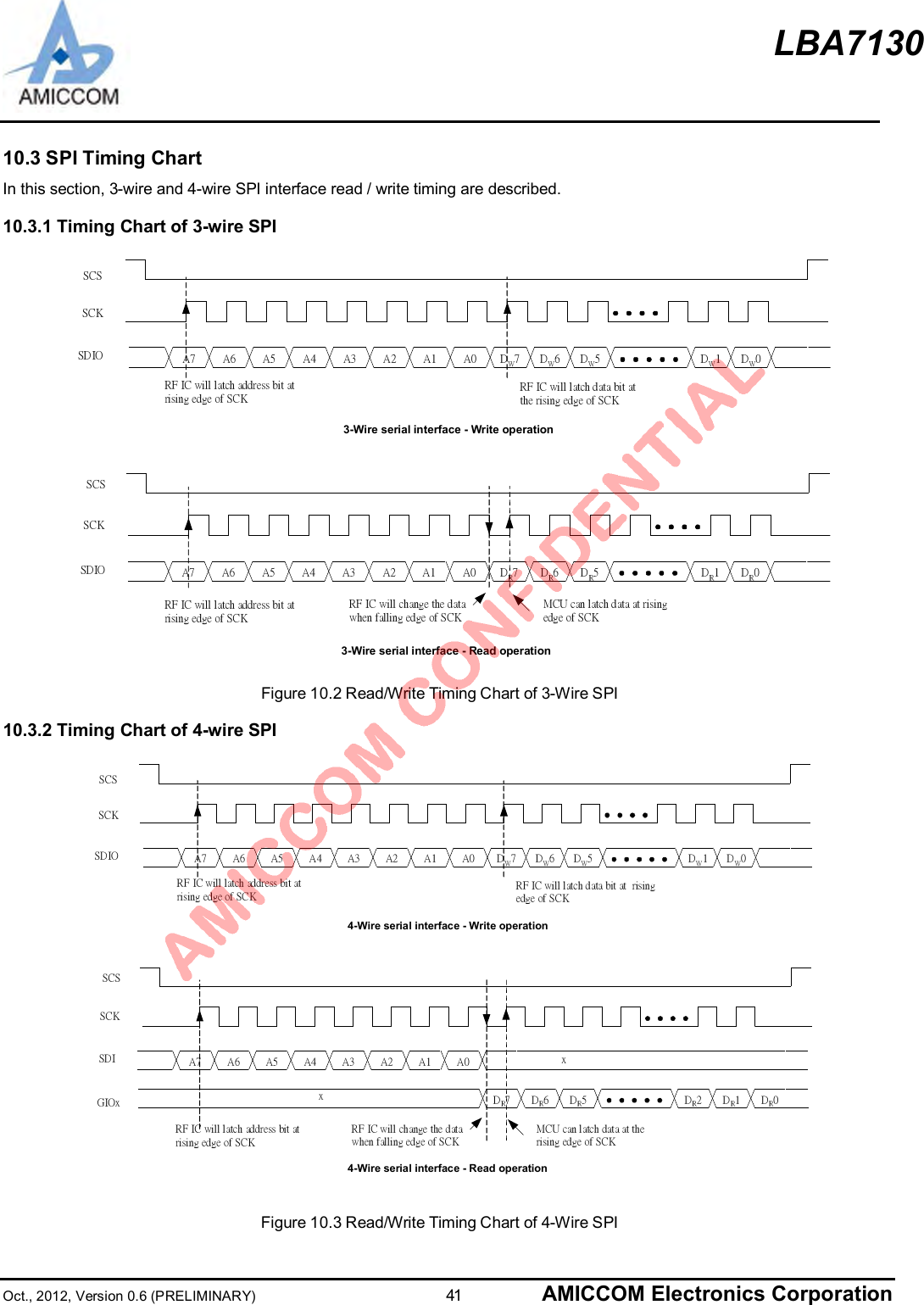
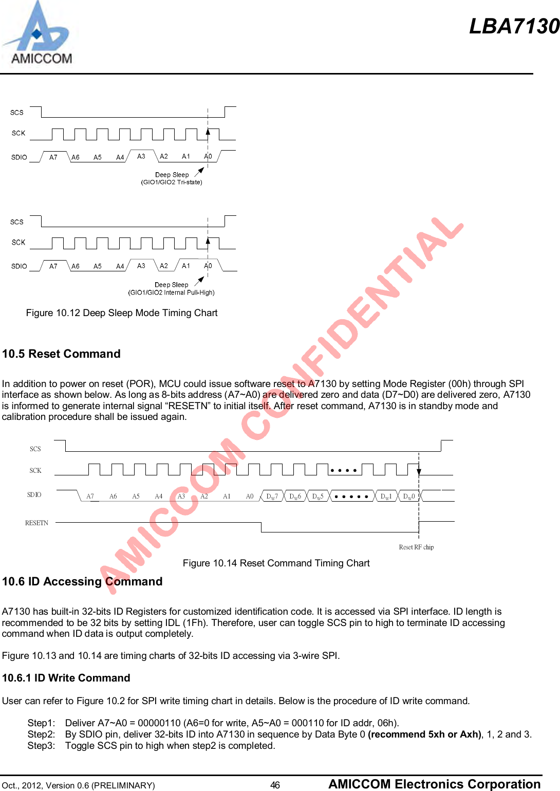
![LBA7130Oct., 2012, Version 0.6 (PRELIMINARY) 39 AMICCOM Electronics Corporation10. SPIA7130 only supports one SPI interface with maximum data rate up to 15Mbps. MCU should assert SCS pin low (SPI chipselect) to active accessing of A7130. Via SPI interface, user can access control registers and issue Strobe command.Figure 10.1 gives an overview of SPI access manners.3-wire SPI (SCS, SCK and SDIO) or 4-wire SPI (SCS, SCK, SDIO and GIO1/GIO2) configuration is provided. For 3-wire SPI,SDIO pin is configured as bi-direction to be data input and output. For 4-wire SPI, SDIO pin is data input and GIO1 (or GIO2)pin is data output. In such case, GIO1S (0bh) or GIO2S (0ch) should be set to [0110].For SPI write operation, SDIO pin is latched into A7130 at the rising edge of SCK. For SPI read operation, if input address islatched by A7130, data output is aligned at falling edge of SCK. Therefore, MCU can latch data output at the rising edge ofSCK.To control A7130’s internal state machine, it is very easy to send Strobe command via SPI interface. The Strobe command isa unique command set with total 8 commands. See section 10.3, 10.4 and 10.5 for details.SPI chip select Data In Data Out3-Wire SPI SCS pin = 0 SDIO pin SDIO pin4-Wire SPI SCS pin = 0 SDIO pin GIO1 (GIO1S=0110) /GIO2 (GIO2S=0110)ADDRreg DataByte ADDRreg ADDRregADDRFIFO DataByte0DataByte1DataByte2DataByte3ADDRID DataByte0DataByte1DataByte2DataByte3StrobeCommandSleep ModeSleep ModeRead/Write IDregisterRead/Write RFFIFORead/Write registerSCSDataBytenDataByte DataByteStrobeCommandIdle ModeIdle ModeStrobeCommandSTBY ModeSTBY ModeStrobeCommandPLL ModePLL ModeStrobeCommandRX ModeRX ModeStrobeCommandTX ModeTX ModeStrobeCommandFIFO Write ResetFIFO Write ResetStrobeCommandFIFO Read ResetFIFO Read ResetFigure 10.1 SPI Access Manners](https://usermanual.wiki/LB-Technology/51402TR/User-Guide-1922627-Page-39.png)
![LBA7130Oct., 2012, Version 0.6 (PRELIMINARY) 40 AMICCOM Electronics Corporation10.1 SPI FormatThe first bit (A7) is critical to indicate A7130 the following instruction is “Strobe command” or “control register”. See Table 10.1for SPI format. Based on Table 10.1, To access control registers, just set A7=0, then A6 bit is used to indicate read (A6=1) orwrite operation (A6=0). See Figure 10.2 (3-wire SPI) and Figure 10.3 (4-wire SPI) for details.Address Byte (8 bits) Data Byte (8 bits)CMD R/W Address DataA7 A6 A5 A4 A3 A2 A1 A0 7 6 5 4 3 2 1 0Table 10.1 SPI FormatAddress byte:Bit 7: Command bit[0]: Control registers.[1]: Strobe command.Bit 6: R/W bit[0]: Write data to control register.[1]: Read data from control register.Bit [5:0]: Address of control registerData Byte:Bit [7:0]: SPI input or output data, see Figure 10.2 and Figure 10.3 for details.10.2 SPI Timing CharacteristicNo matter 3-wire or 4-wire SPI interface is configured, the maximum SPI data rate is 10 Mbps. To active SPI interface, SCSpin must be set to low. For correct data latching, user has to take care hold time and setup time between SCK and SDIO. SeeTable 10.2 for SPI timing characteristic.Parameter Description Min. Max. UnitFCFIFO clock frequency. 10 MHzTSE Enable setup time. 50 nsTHE Enable hold time. 50 nsTSW TX Data setup time. 50 nsTHW TX Data hold time. 50 nsTDR RX Data delay time. 0 50 nsTable 10.2 SPI Timing Characteristic](https://usermanual.wiki/LB-Technology/51402TR/User-Guide-1922627-Page-40.png)
![LBA7130Oct., 2012, Version 0.6 (PRELIMINARY) 47 AMICCOM Electronics CorporationFigure 10.15 ID Write Command Timing Chart10.6.2 ID Read CommandUser can refer to Figure 10.2 for SPI read timing chart in details. Below is the procedure of ID read command.Step1: Deliver A7~A0 = 01000110 (A6=1 for read, A5~A0 = 000110 for ID addr, 06h).Step2: SDIO pin outputs 32-bits ID in sequence by Data Byte 0, 1, 2 and 3.Step3: Toggle SCS pin to high when step2 is completed.Figure 10.16 ID Read Command Timing Chart10.7 FIFO Accessing CommandTo use A7130’s FIFO mode, enable FMS (01h) =1 via SPI interface. Before TX delivery, just write wanted data into TX FIFO(05h) then issue TX Strobe command. Similarly, user can read RX FIFO (05h) once payload data is received.MCU can use polling or interrupt scheme to do FIFO accessing. FIFO status can output to GIO1 (or GIO2) pin by settingGIO1S (0Bh) or GIO2S (0Ch).Figure 10.15 and 10.16 are timing charts of FIFO accessing via 3-wire SPI.10.7.1 TX FIFO Write CommandUser can refer to Figure 10.2 for SPI write timing chart in details. Below is the procedure of TX FIFO write command.Step1: Deliver A7~A0 = 00000101 (A6=0 for write control register and issue FIFO A [5:0] = 05h).Step2: By SDIO pin, deliver (n+1) bytes TX data into TX FIFO in sequence by Data Byte 0, 1, 2 to n.Step3: Toggle SCS pin to high when step2 is completed.Step4: Send Strobe command of TX mode (Figure 10.9) to do TX delivery.](https://usermanual.wiki/LB-Technology/51402TR/User-Guide-1922627-Page-47.png)
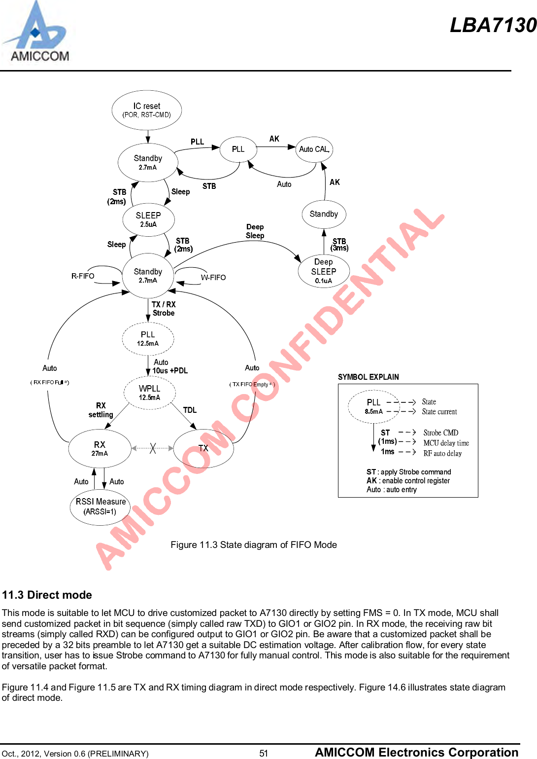
![LBA7130Oct., 2012, Version 0.6 (PRELIMINARY) 50 AMICCOM Electronics Corporation11.2 FIFO modeThis mode is suitable for the requirements of general purpose applications and can be chosen by setting FMS = 1. Aftercalibration, user can issue Strobe command to enter standby mode where write TX FIFO or read RX FIFO. From standbymode to packet data transmission, only one Strobe command is needed. Once transmission is done, A7130 is auto back tostandby mode. Figure 11.1 and Figure 11.2 are TX and RX timing diagram respectively. Figure 11.3 illustrates state diagramof FIFO mode.Strobe CMD(SCS,SCK,SDIO)T0 T2T1TXStrobeGIO1 Pin - WTR(GIO1S[3:0]=0000)RF settling10us +(PDL+TDL)Next InstructionPreamble + ID Code + PayloadRFO PinTransmitting TimeAuto BackStandby ModeFigure 11.1 TX timing of FIFO ModeStrobe CMD(SCS,SCK,SDIO)T0 T3T2RXstrobeGIO1 Pin - WTR(GIO1S[3:0]=0000)RX settlingNext InstructionPreamble + ID Code + PayloadRFI PinReceiving TimeAuto BackStandby ModeT1WaitPacketFigure 11.2 RX timing of FIFO Mode](https://usermanual.wiki/LB-Technology/51402TR/User-Guide-1922627-Page-50.png)
![LBA7130Oct., 2012, Version 0.6 (PRELIMINARY) 52 AMICCOM Electronics CorporationStrobe CMD(SCS,SCK,SDIO)T0 T4T1TXStrobeGIO1 Pin - WTR(GIO1S[3:0]=0000)RF settling10us+(PDL+TDL)STB strobePreamble + customized raw TXDRFO PinManually backto STBGIO1 Pin - TMEO(GIO1S[3:0]=0010)GIO2 Pin - TXD(GIO2S[3:0]=1001)CarrieronlyModulated signals32-bitspreambleModulation auto enableT3Figure 11.4 TX timing of Direct ModeStrobe CMD(SCS,SCK,SDIO)T0 T4T1RXStrobeGIO1 Pin - WTR(GIO1S[3:0]=0000)RX settlingSTB strobePreamble + customized raw TXDRFO PinManually backto STBGIO1 Pin - PMDO(GIO1S[3:0]=0011)GIO2 Pin - RXD(GIO2S[3:0]=1000)Waitpacket Coming packetPreamble detect outputT3Figure 11.5 RX timing of Direct Mode](https://usermanual.wiki/LB-Technology/51402TR/User-Guide-1922627-Page-52.png)
![LBA7130Oct., 2012, Version 0.6 (PRELIMINARY) 54 AMICCOM Electronics Corporation12. Crystal OscillatorA7130 needs external crystal or external clock that is either 16 MHz (or 18MHz) to generate internal wanted clock.Relative Control RegisterClock Register (Address: 0Dh)Name R/W Bit 7 Bit 6 Bit 5 Bit 4 Bit 3 Bit 2 Bit 1 Bit 0Clock W CGC1 CGC0 GRC3 GRC2 GRC1 GRC0 CGS XSRIFS1 IFS0 GRC3 GRC2 GRC1 GRC0 -- --12.1 Use External CrystalFigure 12.1 shows the connection of crystal network between XI and XO pins. C1 and C2 capacitance built inside A7130 areused to adjust different crystal loading. User can set INTXC [4:0] to meet crystal loading requirement. A7130 supports lowcost crystal within ± 50 ppm accuracy. Be aware that crystal accuracy requirement includes initial tolerance, temperature drift,aging and crystal loading.Crystal Accuracy Crystal ESR±50 ppm ≦80 ohmFig12.1 Crystal oscillator circuit, set INTXC[4:0] for the internal C1 and C2 values.12.2 Use External ClockA7130 has built-in AC couple capacitor to support external clock input. Figure 12.2 shows how to connect. In such case, XI pinis left opened. XS shall be low to select external clock. The frequency accuracy of external clock shall be controlled within ± 50ppm, and the amplitude of external clock shall be within 1.2 ~ 1.8 V peak-to-peak.Fig12.2 External clock source. R is used to tune Vpp = 1.2~1.8V](https://usermanual.wiki/LB-Technology/51402TR/User-Guide-1922627-Page-54.png)
 Note16MHz 0 0111 0 1 00 10 1 11 0x00 FIFO mode16MHz 1 1111 0 1 00 10 1 11 0x00 Direct mode](https://usermanual.wiki/LB-Technology/51402TR/User-Guide-1922627-Page-55.png)
![LBA7130Oct., 2012, Version 0.6 (PRELIMINARY) 56 AMICCOM Electronics Corporation14. Transceiver LO FrequencyA7130 is a half-duplex transceiver with embedded PA and LNA. For TX or RX frequency setting, user just needs to set up LO(Local Oscillator) frequency for two ways radio transmission.To target full range of 2.4GHz ISM band (2408 MHz to 2468 MHz), A7130 applies offset concept by LO frequency FLO =FLO_BASE + FOFFSET. Therefore, this device is easy to implement frequency hopping and multi-channels by just ONE registersetting, PLL Register I (CHN [7:0]).Below is the LO frequency block diagram./ (RRC[1:0]+1)X (DBL+1) PFD VCO+DividerFXTALCHN / [4*(CHR+1)]AC[14:0]/ 216010AFCFPFD FLOFLOBIP[8:0] +BFP[15:0]/ 216+FLO_BASEFOFFSETFig14.1 Frequency synthesizer block diagram14.1 LO Frequency SettingFrom Figure 14.1, FLO is not only for TX radio frequency but also to be RX LO frequency. To set up FLO, it is easy by below 4steps.1. Set FLO_BASE ~ 2400.001MHz.2. Set FCHSP = 500 KHz.3. Set FOFFSET = CHN [7:0] x FCHSP4. The LO frequency, FLO = FLO_BASE + FOFFSETFLO_BASE)2]0:15[]0:8[(1]0:1[)1()2]0:15[]0:8[( 1616PFDLO_BASEBFPBIPRRCFDBLBFPBIPFF XTAL +×+×+=+×=Base on the above formula, i.e. 16 MHz, please refer to Table 14.1 and 14.2 as a calculation example to get LO frequency.DBL = 0 for FIFO modeSTEP ITEMS VALUE NOTE1 FXTAL 16 MHz Crystal Frequency2DBL 0 Disable double functionFOFFSETFLO_BASEFLO](https://usermanual.wiki/LB-Technology/51402TR/User-Guide-1922627-Page-56.png)
![LBA7130Oct., 2012, Version 0.6 (PRELIMINARY) 57 AMICCOM Electronics Corporation3RRC 0 If so, FPFD= 16MHz4BIP[8:0] 0x096 To get FLO_BASE =2400 MHz5 BFP[15:0] 0x0004 To get FLO_BASE ~ 2400.001 MHz6 FLO_BASE 2400.001 MHz LO Base frequencyDBL = 1 for Direct modeSTEP ITEMS VALUE NOTE1 FXTAL 16 MHz Crystal Frequency2DBL 1 Enable double function3RRC 0 If so, FPFD= 16MHz4BIP[8:0] 0x04B To get FLO_BASE =2400 MHz5 BFP[15:0] 0x0002 To get FLO_BASE ~ 2400.001 MHz6 FLO_BASE 2400.001 MHz LO Base frequencyTable 14.1 How to set FLO_BASEHow to set FTXRF = FLO = FLO_BASE + FOFFSET ~ 2405.001 MHzSTEP ITEMS VALUE NOTE1 FLO_BASE 2400.001 MHz After set up BIP and BFP[0111] To get FCHSP= 500 KHz if DBL =0 for FIFO mode.2 CHR[3:0][1111] To get FCHSP= 500 KHz if DBL =1 for Direct mode.4CHN[7:0] 0x0A FOFFSET= 500 KHz * (CHN) = 5MHz6 FLO 2405.001 MHz Get FLO= FLO_BASE + FOFFSET7 FTXRF 2405.001 MHz FTXRF = FLOTable 14.2 How to set FTXRFFor 16MHz crystal, below is the calculation detail for FFPD and FCHSP.[]( )10:34 +×=CHRFFPFDCHSPFXTAL (M Hz) DBL(0Fh)RRC(0Fh) FPFD (MHz) CHR [3:0] FCHSP (KHz) Note16 0 00 16 0111 500 Recommend16 1 00 32 1111 500 Recommend14.2 IF Side Band SelectSince A7130 is a low-IF TRX, in RX mode, the FRXLO shall be set to shift a FIF (i.e. FIF = 4MHz @ 4Mbps) regarding to comingFTXRF. Therefore, A7130 offers two methods to set up FLO while A7130 is exchanging from TX mode to RX mode.AIF register is used to enable Auto IF function for Auto IF exchange mode. And ULS registers is used for fast exchange modebecause of reduction of PLL settling time.(1) Auto IF exchange modeAIF (01h) ULS (19h) FRXLO Formula Note1 0 FRXLO = FLO - FIF Auto-minus a FIF because ULS = 01 1 FRXLO = FLO + FIF Auto-plus a FIF because ULS = 1(2) Fast exchange modeAIF (01h) ULS (19h) FRXLO Formula Note0 0 FRXLO = FLO The coming FTXRF shall be (FRXLO + FIF )0 1 FRXLO = FLO The coming FTXRF shall be (FRXLO - FIF )](https://usermanual.wiki/LB-Technology/51402TR/User-Guide-1922627-Page-57.png)
![LBA7130Oct., 2012, Version 0.6 (PRELIMINARY) 58 AMICCOM Electronics Corporation14.2.1 Auto IF ExchangeA7130 supports Auto IF offset function by setting AIF = 1. In such case, FTXRF between master and slave is the same so thatthere is only one carrier frequency (Fcarrier) during communications. Meanwhile, FRXLO during TRX exchanging is auto shiftedFIF. See below Figures and Table 14.3 for details.MasterAIF=1 and ULS=0, FRXLO is auto shifted lower than FTXRF for a (FIF).Master AIF ULS CHN[7:0] FCHSP (KHz) FLO_BASE (MHz) FTXRF (MHz) FRXLO (MHz)TX 1 0 0x0A 500 2400.001 2405.001 --RX 1 0 0x0A 500 2400.001 -- 2401.001SlaveAIF=1 and ULS=0, FRXLO is auto shifted lower than FTXRF for a (FIF).Slave AIF ULS CHN[7:0] FCHSP (KHz) FLO_BASE (MHz) FTXRF (MHz) FRXLO (MHz)TX 1 0 0x0A 500 2400.001 2405.001 --RX 1 0 0x0A 500 2400.001 -- 2401.001Table 14.3 Auto IF exchange mode while TRX exchangingFOFFSET =5MHzFIF4MHz @ 4MbpsFRXLOFLO_BASEFTXRF= FLO=FCarrierFOFFSET =5MHzFRXLOFLO_BASEFTXRF= FLO=FCarrierFIF4MHz @ 4Mbps](https://usermanual.wiki/LB-Technology/51402TR/User-Guide-1922627-Page-58.png)
![LBA7130Oct., 2012, Version 0.6 (PRELIMINARY) 59 AMICCOM Electronics Corporation14.2.2 Fast ExchangeFast exchange can reduce the PLL settling time during TRX exchanging because FRXLO and FTXRF are kept to the same FLO ineither master or slave side. However, there are two on-air frequency (FCarrier (master), FCarrier (slave)) during communications. In suchcase, user has to control ULS =0 in master side and ULS = 1 in slave side for two ways radio. See below Figures and Table 14.4for details.MasterAIF=0 and ULS=0, Master is set to up side band.SlaveAIF=0 and ULS=1, Slave is set to low side band.Master AIF ULS CHN[7:0] FCHSP (KHz) FLO_BASE (MHz) FTXRF (MHz) FRXLO (MHz)TX 0 0 0x0A 500 2400.001 2405.001 --RX 0 0 0x0A 500 2400.001 -- 2405.001Slave AIF ULS CHN[7:0] FCHSP (KHz) FLO_BASE (MHz) FTXRF (MHz) FRXLO (MHz)TX 0 1 0x12 500 2400.001 2409.001 --RX 0 1 0x12 500 2400.001 -- 2409.001Table 14.4 Fast exchange mode while TRX exchangingFIF4MHz @ 4MbpsFRXLOFOFFSET =9MHzFLO_BASEFRXLOFLO_BASEFTXLO=FLO=FCarrier (Master)FOFFSET =5MHzFTXLO=FLO=FCarrier (Slave)](https://usermanual.wiki/LB-Technology/51402TR/User-Guide-1922627-Page-59.png)
![LBA7130Oct., 2012, Version 0.6 (PRELIMINARY) 60 AMICCOM Electronics Corporation14.3 Auto Frequency CompensationThe AFC function (Auto Frequency Compensation) supports to use low accuracy crystal (±50 ppm) on A7130 without sensitivitydegradation. The AFC concept is automatically fine tune RX LO frequency (FRXLO). User can read AC [14:0] to know thecompensation value of FRXLO./ (RRC[1:0]+1)X (DBL+1) PFD VCO+DividerFXTALCHN / [4*(CHR+1)]AC[14:0]/ 216010AFCFPFD FLOFLOBIP[8:0] +BFP[15:0]/ 216+FLO_BASEFOFFSETFigure 14.3 Block Diagram of enabling AFC functionFor AFC procedure, please refer to A7130’s reference code and contact AMICCOM FAE team for details.15. CalibrationA7130 needs calibration process after deep sleep mode or power on reset or software reset. Below are six calibration itemsinside the device.1. VCO Current Calibration.2. VCO Bank Calibration.3. VCO Deviation Calibration.4. IF Filter Bank Calibration.5. RSSI Calibration.6. RC Oscillator Calibration.15.1 Calibration ProcedureThe purpose to execute the above calibration items is to deal with Foundry process deviation. After calibrations, A7130 will beset to the best working conditions without concerning Foundry process deviation to impact A7130’s RF performance.In general, user can use A7130’s auto calibration function by just enabling calibration items and checking its calibration flag. Fordetailed calibration procedures, please refer to A7130 reference code of initRF() subroutine and A7130_Cal() subroutine.1. Initialize A7130 by calling the subroutine of initRF().n Initialize all control registers by calling the subroutine of A7130_Config().n Execute all calibration items by calling the subroutine of A7130_Cal().](https://usermanual.wiki/LB-Technology/51402TR/User-Guide-1922627-Page-60.png)
![LBA7130Oct., 2012, Version 0.6 (PRELIMINARY) 61 AMICCOM Electronics Corporation16. FIFO (First In First Out)A7130 has the separated physical 64-bytes TX and RX FIFO inside the device. To use A7130’s FIFO mode, user just needs toenable FMS =1. For FIFO accessing, TX FIFO (write-only) and RX FIFO (read-only) share the same register address 05h. TXFIFO represents transmitted payload. On the other hand, RX circuitry synchronizes ID Code and stores received payload intoRX FIFO.16.1 TX Packet Format in FIFO mode16.1.1 Basic FIFO modeIf FCL[1:0] = 00 and ENRL = 0, A7130 is formed a Basic FIFO mode which can also support Auto-ack/ Auto-resend function.There is no MAC header in TX packet format. ID code is a PHY header used to be the frame sync to enable RX FIFO receiving.ID codePreamble Payload (CRC)4 bytes 4 bytes 2 bytesPhy. 64 bytesCRC -16 calculation(optional)FEC encoded/decoded(optional)Data whitening(optional)Figure 16.1 TX packet format of basic FIFO modePreamble:The packet is led by a self-generated preamble which is composed of alternate 0 and 1. If the first bit of ID code is 0, preambleshall be 0101…0101. In the contrast, if the first bit of ID code is 1, preamble shall be 1010…1010.Preamble length is recommended to set 4 bytes by PML [1:0] (20h).ID code:ID code is recommended to set 4 bytes by IDL[1:0] = [01] and ID Code is stored into ID Data register by sequence ID Byte 0, 1,2 and 3. If RX circuitry check ID code is correct, payload will be written into RX FIFO. In addition, user can set ID code errortolerance (0~ 7bit error) by setting ETH [2:0] during ID synchronization check.Payload:Payload length is programmable by FEP [11:0]. The physical FIFO depth is 64 bytes. A7130 also supports logical FIFOextension up to 4K bytes.CRC:In FIFO mode, if CRC is enabled (CRCS=1), 2-bytes of CRC value is self-generated and attached at the footer of the packet. Inthe same way, RX circuitry will check CRC value and show the result to CRC Flag.16.1.2 Advanced FIFO modeA7130 supports to self generated MAC header to form an advanced FIFO mode by enabling FCL[1:0], ENRL.. Therefore,A7130 can support ACK FIFO (FCB1~FCB3) and dynamic FIFO length depending on configurations.ID codeID Byte 0 ID Byte 1 ID Byte 2 ID Byte 3](https://usermanual.wiki/LB-Technology/51402TR/User-Guide-1922627-Page-61.png)
![LBA7130Oct., 2012, Version 0.6 (PRELIMINARY) 62 AMICCOM Electronics CorporationID codePreamble Payload (CRC)4 bytes 4 bytes 2 bytesPhy. 64 bytesFCB1~4 bytesFEP1 2 b itsau toack/resenddynamicFIFOM AC H eader (self-generated)PH Y H eader (self-generated)Figure 16.2 TX packet format of advanced FIFO mode.FCB:If FCL[1:0] ≠00, FCB header is enabled to support ACK FIFO by (FCB1~FCB3). The FCB is frame control byte. FCB0 is NOTallowed to program but carry a dedicated header (00111b) and SID [2:0] (Serial ID of packet number). FCB1~3 are used forcustomized information in FCB field.Figure 16.3 FCB (Frame Control Field)FEP:If ENRL = 1, A7130 supports dynamic FIFO. FEP [11:0] is self-generated to add into TX packet. In RX side, FEP[11:0] of thecoming TX packet will be detected and stored into LENF [11:0] register.HEC:If HECS = 1, A7130 supports to self-generated a HEC byte which is a local CRC-8 of the MAC header. This HEC byte is anoptional feature to calculate CRC result of MAC Header. HEC is located at the end of the MAC header.ID codePreamble Payload (CRC)4 bytes 4 bytes 2 bytesPhy. 64 bytesFCB1~4 bytesFEP12 b itsHEC1 b yteHeaderCRCM A C H eader (self-generated)PH Y H eader (self-generated)MACheaderFigure 16.4 HEC (CRC for MAC Header)16.2 Bit Stream Process in FIFO modeA7130 supports 3 optional bit stream process for payload in FIFO mode, they are,(1) CCITT-16 CRC(2) (7, 4) Hamming FEC(3) Data Whitening by XOR PN7 (7-bits Pseudo Random Sequence). The initial seed of PN7 is set by WS [6:0]CRC (Cyclic Redundancy Check):1. CRC is enabled by CRCS= 1. TX circuitry calculates the CRC value of payload (preamble and ID code are excluded) andtransmits 2-bytes CRC value after payload.2. RX circuitry checks CRC value and shows the result to CRCF. If CRCF=0, received payload is correct, else erroroccurred.FCBFCB 0 FCB 1 FCB 2 FCB 3](https://usermanual.wiki/LB-Technology/51402TR/User-Guide-1922627-Page-62.png)
![LBA7130Oct., 2012, Version 0.6 (PRELIMINARY) 63 AMICCOM Electronics CorporationFEC (Forward Error Correction):1. FEC is enabled by FECS= 1. Payload and CRC value (if CRCS=1) are encoded by (7, 4) Hamming code.2. Each 4-bits (nibble) of payload is encoded into 7-bits code word and delivered out automatically.(ex., 64 bytes payload will be encoded to 128 code words, each code word is 7 bits.)3. RX circuitry decodes received code words automatically. Each code word can correct 1-bit error. Once 1-bit erroroccurred, FECF=1 (00h).Data Whitening:1. Data whitening is enabled by WHTS= 1. Payload and CRC value (if CRCS=1) or their encoded code words (if FECS=1)are encrypted by bit XOR operation with PN7. The initial seed of PN7 is set by WS [6:0].2. RX circuitry decrypts received payload and 2-bytes CRC (if CRCS=1) automatically. Please noted that user shall set thesame WS [6:0] (22h) to TX and RX.16.3 Transmission TimeBased on CRC and FEC options, the transmission time are different. See table 16.1 for details.Data Rate = 4 MbpsData Rate Preamble(bits)ID Code(bits)Payload(bits)CRC(bits)FEC TransmissionTime / Packet32 32 512 Disable Disable 576 bit X 0.25 us = 144 us32 32 512 16 bits Disable 592 bit X 0.25 us = 148 us32 32 512 Disable 512 x 7 / 4 960 bit X 0.25 us = 240 us4Mbps32 32 512 16 x 7 / 4 512 x 7 / 4 988 bit X 0.25 us = 247 usTable 16.1 Transmission time16.4 Usage of TX and RX FIFOIn application points of view, A7130 supports 2 options of FIFO arrangement.(1) Easy FIFO(2) Segment FIFO(3) FIFO extensionFor FIFO operation, A7130 supports Strobe command to reset TX and RX FIFO pointer as shown below. User can refer tosection 10.5 for details.Strobe CommandStrobe CommandA7 A6 A5 A4 A3 A2 A1 A0 Description1 1 1 0 x x X x FIFO write pointer reset (for TX FIFO)1 1 1 1 x x X x FIFO read pointer reset (for RX FIFO)](https://usermanual.wiki/LB-Technology/51402TR/User-Guide-1922627-Page-63.png)
![LBA7130Oct., 2012, Version 0.6 (PRELIMINARY) 64 AMICCOM Electronics Corporation16.4.1 Easy FIFOIn Easy FIFO mode, max FIFO length is 64 bytes. FIFO length is equal to ( FEP [11:0] +1 ) where FEP [11:0] is max 0x003F.User just needs to control FEP [11:0] (03h) and disable PSA and FPM as shown below.TX-FIFO(byte)RX-FIFO(byte)FEP[11:0](03h)PSA[5:0](04h)FPM[1:0](04h)1 1 0x00 0 08 8 0x07 0 016 16 0x0F 0 032 32 0x1F 0 064 64 0x3F 0 0 Table 16.2 Control registers of Easy FIFOProcedures of TX FIFO Transmitting1. Initialize all control registers (refer A7130 reference code).2. Set FEP [11:0] = 0x003F for 64-bytes FIFO.3. Send Strobe command – TX FIFO write pointer reset.4. MCU writes 64-bytes data to TX FIFO.5. Send TX Strobe Command and monitor WTR signal.6. D one.Procedures of RX FIFO Reading1. When RX FIFO is full, WTR (or FSYNC) can be used to trigger MCU for RX FIFO reading.2. Send Strobe command – RX FIFO read pointer reset.3. MCU monitors WTR signal and then read 64-bytes from RX FIFO.4. D one.Figure 16.5 Easy FIFO](https://usermanual.wiki/LB-Technology/51402TR/User-Guide-1922627-Page-64.png)
![LBA7130Oct., 2012, Version 0.6 (PRELIMINARY) 65 AMICCOM Electronics Corporation16.4.2 Segment FIFOIn Segment FIFO, TX FIFO length is equal to (FEP [11:0] - PSA [5:0]+1). FPM [1:0] should be zero. This function is veryuseful for button applications. In such case, each button is used to transmit fixed code (data) every time. During initialization,each fixed code is written into corresponding segment FIFO once and for all. Then, if button is triggered, MCU just assignscorresponding segment FIFO (PSA [5:0] and FEP [11:0]) and issues TX strobe command. Table 16.4 explains the details if TXFIFO is arranged into 8 segments, each TX segment and RX FIFO length are 8 bytes.Segment PSA FEP TX FIFO Length PSA[5:0] FEP[11:0] FPM[1:0]1PSA1 FEP1 8 bytes 0x00 0x07 02PSA2 FEP2 8 bytes 0x08 0x0F 03PSA3 FEP3 8 bytes 0x10 0x17 04PSA4 FEP4 8 bytes 0x18 0x1F 05PSA5 FEP5 8 bytes 0x20 0x27 06PSA6 FEP6 8 bytes 0x28 0x2F 07PSA7 FEP7 8 bytes 0x30 0x37 08PSA8 FEP8 8 bytes 0x38 0x3F 0RX FIFO Length PSA[5:0] FEP[11:0] FPM[1:0]8 bytes 0 0x0007 0Table 16.3 Segment FIFO is arranged into 8 segmentsProcedures of TX FIFO Transmitting1. Initialize all control registers (refer A7130 reference code).2. Issue Strobe command – TX FIFO write pointer reset.3. MCU writes fixed code into corresponding segment FIFO once and for all.4. To consign Segment 1, set PSA = 0x00 and FEP= 0x0007To consign Segment 2, set PSA = 0x08 and FEP= 0x000FTo consign Segment 3, set PSA = 0x10 and FEP= 0x0017To consign Segment 4, set PSA = 0x18 and FEP= 0x001FTo consign Segment 5, set PSA = 0x20 and FEP= 0x0027To consign Segment 6, set PSA = 0x28 and FEP= 0x002FTo consign Segment 7, set PSA = 0x30 and FEP= 0x0037To consign Segment 8, set PSA = 0x38 and FEP= 0x003F5. Issue TX Strobe Command and monitor WTR signal.6. D one.Procedures of RX FIFO Reading1. When RX FIFO is full, WTR (or FSYNC) is used to trigger MCU for RX FIFO reading.2. Issue Strobe command – RX FIFO read pointer reset.3. MCU monitors WTR signal and then read 8-bytes from RX FIFO.4. D one.](https://usermanual.wiki/LB-Technology/51402TR/User-Guide-1922627-Page-65.png)
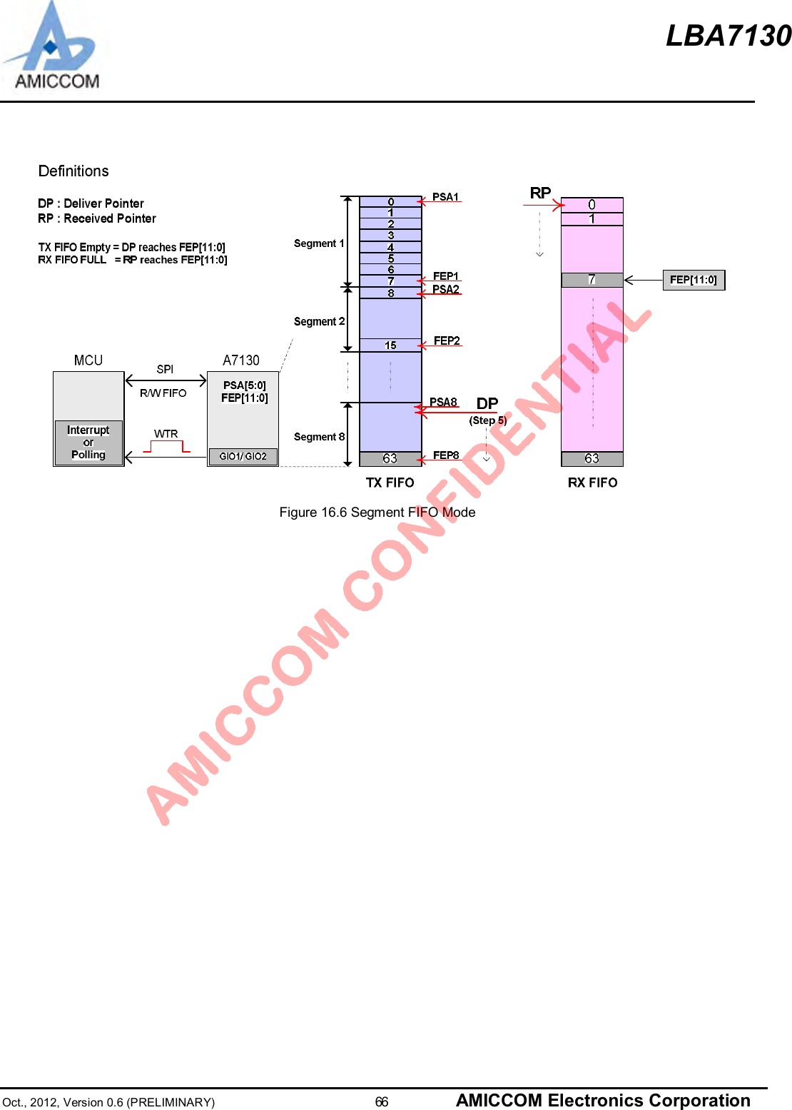
![LBA7130Oct., 2012, Version 0.6 (PRELIMINARY) 67 AMICCOM Electronics Corporation16.4.3 FIFO ExtensionA7130 supports FIFO extension up to 4K bytes from the 64 bytes physical TX FIFO and RX FIFO. The FIFO extension length isconfigured by (FEP [11:0] +1 and PSA [5:0] =0). FPM [1:0] is used to set the FPF threshold which FPF is FIFO Pointer Flag toinform MCU the timing of reading RX FIFO and refilling TX FIFO.Please be notice, SPI speed is important to prevent error operation (over-write) in FIFO extension mode. We recommend themin. SPI speed shall be equal or greater than (A70 on-air data rate + 500Kbps).Please refer to A7130’s reference code(FIFO extension) for details.For example, if A7130 data rate = 4Mbps and FIFO extension = 256 bytes.TX RX Control RegistersFIFOLength(byte)FPFThresholdMax. SPIData RateFIFOLength(byte)FPFThresholdMax. SPIData RateFEP[7:0] FPM[1:0] PSA[5:0]Delta = 04 10 Mbps Delta = 60 10 Mbps 00 0Delta = 08 10 Mbps Delta = 56 10 Mbps 01 0Delta = 12 10 Mbps Delta = 52 10 Mbps 10 0256Delta = 16 8 Mbps256Delta = 48 8 Mbps0xFF11 0Table 16.4 How to set FIFO extension when A7130 is at 4Mbps data rateProcedures of TX FIFO Extension1. Initialize all control registers (refer A7130 reference code).2. Set FEP [11:0] = 0x0FF for 256-bytes FIFO extension.3. Set FPM [1:0] = 11 for FPF threshold.4. Set CKO Register = 0x125. Issue Strobe command – TX FIFO write pointer reset.6. MCU writes 1st 64-bytes TX FIFO.7. Issue TX Strobe command.8. MCU monitors FPF from A7130’s CKO pin.9. FPF triggers MCU to write 2nd 48-bytes TX FIFO.10. Monitor FPF.11. FPF triggers MCU to write 3rd 48-bytes TX FIFO.12. Monitor FPF.13. FPF triggers MCU to write 4th 48-bytes TX FIFO.14. Monitor FPF.15. FPF triggers MCU to write 5th 48-bytes TX FIFO.16. D one.](https://usermanual.wiki/LB-Technology/51402TR/User-Guide-1922627-Page-67.png)
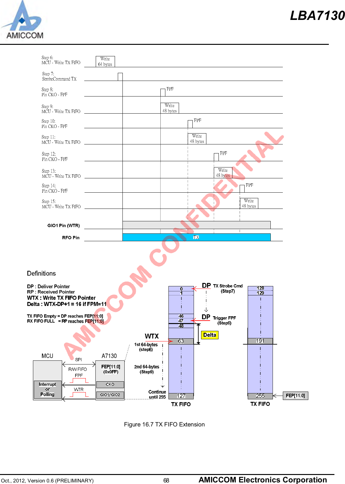
![LBA7130Oct., 2012, Version 0.6 (PRELIMINARY) 69 AMICCOM Electronics CorporationProcedures of RX FIFO Reading1. Initialize all control registers (refer A7130 reference code).2. Set FEP [11:0] = 0x0FF for 256-bytes FIFO extension.3. Set FPM [1:0] = [11b] for FPF threshold.4. Set CKO Register = 0x125. Issue Strobe command – RX FIFO read pointer reset.6. Issue RX Strobe command.7. MCU monitors FPF from A7130’s CKO pin.8. FPF triggers MCU to read 1st 48-bytes RX FIFO.9. Monitor FPF.10. FPF triggers MCU to read 2nd 48-bytes RX FIFO.11. Monitor FPF.12. FPF triggers MCU to read 3rd 48-bytes RX FIFO.13. Monitor FPF.14. FPF triggers MCU to read 4th 48-bytes RX FIFO.15. Monitor FPF.16. FPF triggers MCU to read 5th 48-bytes RX FIFO.17. Monitor WTR falling edge or WTR = low, read the rest 16-bytes RX FIFO18. D one.](https://usermanual.wiki/LB-Technology/51402TR/User-Guide-1922627-Page-69.png)
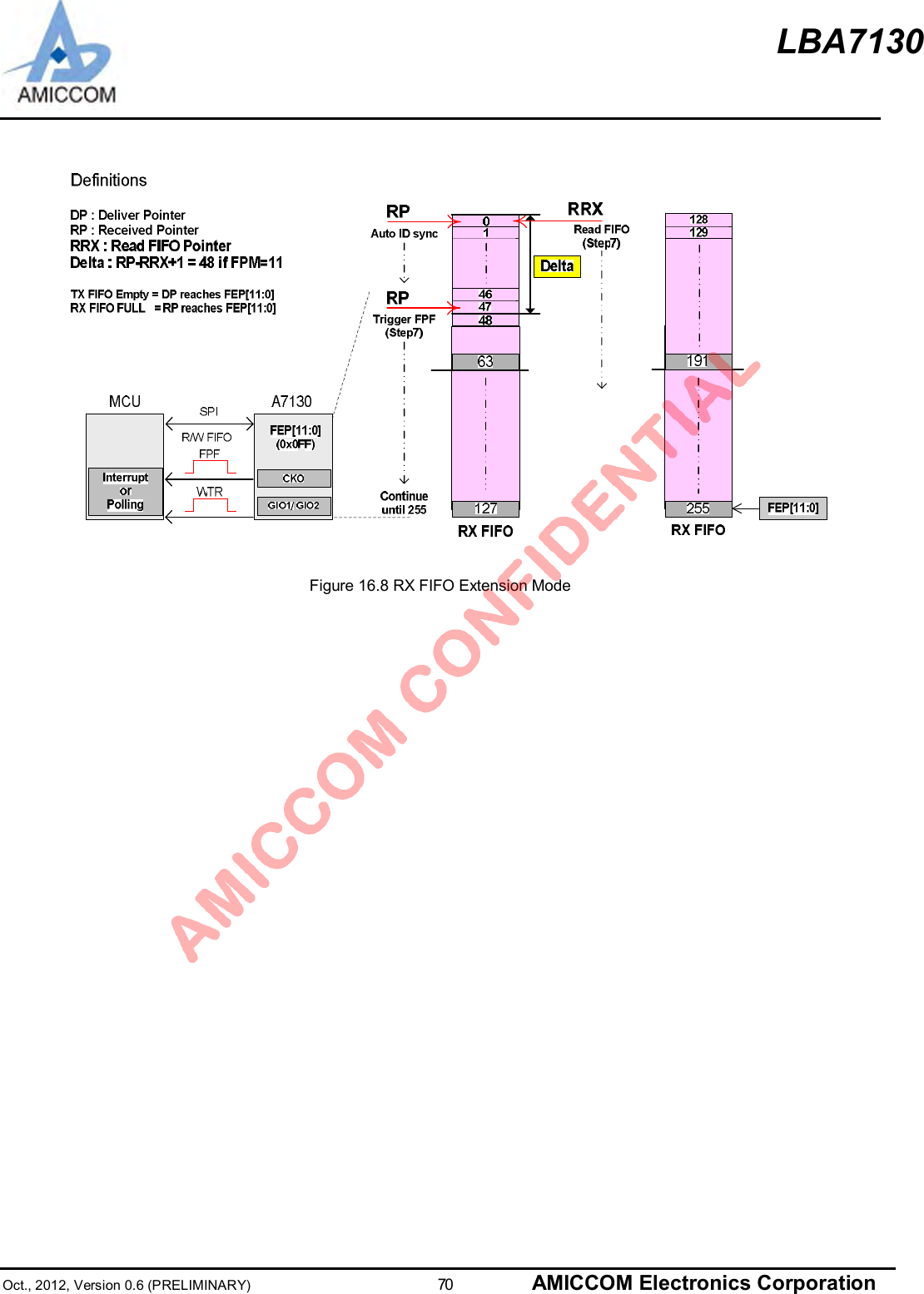
![LBA7130Oct., 2012, Version 0.6 (PRELIMINARY) 71 AMICCOM Electronics Corporation17. ADC (Analog to Digital Converter)A7130 has built-in 8-bits ADC for RSSI measurement and internal thermal sensor by enabling ADCM. User can just use therecommended va lues of ADC from Tab le 17.1. P lease noted tha t ADC clock can be selected by s etting FSARS (4MHz or8MHz). The ADC converting time is 20 x ADC clock periods.XADS(1Fh)RSS(1Ch)ARSSI(01h)ADCM(01h)ERSSM(1Ch)FSARS(1Fh)CDM(1Fh) Standby Mode RX Mode0111101Thermal sensor RSSITable 17.1 Setting of RSSI measurement17.1 RSSI MeasurementA7130 supports 8-bits digital RSSI to detect RF signal strength. RSSI value is stored in ADC [7:0] (1Eh). Fig 17.1 shows atypical plot of RSSI reading as a function of input power. Be aware RSSI accuracy is about ± 6dBm.ADC value Curve (AGC on,25℃)050100150200250300-110 -105 -100 -95 -90 -85 -80 -75 -70 -65 -60 -55 -50 -45 -40 -35 -30 -25 -20 -15 -10 -5 0 5 10Input Power (dBm)ADC ValueAverageADC value Curve (AGC off,25℃)050100150200250-110 -105 -100 -95 -90 -85 -80 -75 -70 -65 -60 -55 -50 -45 -40 -35 -30 -25 -20 -15 -10 -5 0 5 10Input Power (dBm)ADC ValueAverageFigure 17.1 Typical RSSI characteristic](https://usermanual.wiki/LB-Technology/51402TR/User-Guide-1922627-Page-71.png)
![LBA7130Oct., 2012, Version 0.6 (PRELIMINARY) 72 AMICCOM Electronics CorporationAuto RSSI measurement for TX Power of the coming packet:1. Set wanted FRXLO.2. Set recommend values of Table 17.1.3. Enable ADCM = 1.4. Send RX Strobe command.5. Once frame sync (FSYNC) is detected or exiting RX mode, user can read digital R SSI value from ADC [7:0] for TX powerof the coming packet.Figure 17.2 RSSI Measurement of TX RSSI of the coming packet.Auto RSSI measurement for Background Power:1. Set wanted FRXLO.2. Set recommend values of Table 17.1.3. Enable ADCM = 1.4. Send RX Strobe command.5. Stay in RX mode at least 140 us and then exiting RX mode. User can read digital RSSI value from ADC [7:0] for thebackground power.Figure 17.3 Measurement of Background RSSI.St robe CMD(SCS,SCK,SDIO)T0RX ModeT0-T1: Settling TimeT2-T3: Receiving PacketT3 : Exit RX mode automatically in FIFO modeT3-T4: MCU read RSSI value @ ADC [7:0]T1RX-StrobeRX Ready Ti meReceived PacketGIO1 Pin - WTR(GPIO1S[3:0]=0000)RF-INT2GIO2 Pin - FSYNC(GPIO2S[3:0]=0001)T4MCU Read ADC[7:0]T3Read 8 -bits RSSI valueStrobe CMD(SCS,SCK,SDIO)T0T0-T1: MCU Delay Loop from PLL to RX mode for RSSI measurmentT1 : Auto RSSI Measurment is done by 8-times average. MCU can read RSSI value from ADC [7:0]RX-StrobeMin. 140 usNo PacketGIO1 Pin - WTR(GPIO1S[3:0]=0000)RFI PinT1GIO2 Pin - FSYNC(GPIO2S[3:0]=0001)MCU Read ADC[7:0]MCU reads 8-bits RSSI value that is refresh every 40 us](https://usermanual.wiki/LB-Technology/51402TR/User-Guide-1922627-Page-72.png)
![LBA7130Oct., 2012, Version 0.6 (PRELIMINARY) 73 AMICCOM Electronics Corporation18. Battery DetectA7130 has a built-in battery detector to check supply voltage (REGI pin). The detecting range is 2.0V ~ 2.7V into 8 levels.Battery detect Register (Address: 2Ch)Name R/W Bit 7 Bit 6 Bit 5 Bit 4 Bit 3 Bit 2 Bit 1 Bit 0WLVR RGV1 RGV0 QDS BVT2 BVT1 BVT0 BD_EBattery detect R-- RGV1 RGV0 BDF BVT2 BVT1 BVT0 BD_EBVT [2:0]: Battery voltage detect threshold.[000]: 2.0V. [001]: 2.1V. [010]: 2.2V. [011]: 2.3V.[100]: 2.4V. [101]: 2.5V. [110]: 2.6V. [111]: 2.7V.BD_E: Battery Detect Enable.[0]: Disable. [1]: Enable. It will be clear after battery detection is triggered.BDF: Battery detection flag.[0]: Battery voltage less than threshold. [1]: Battery voltage greater than threshold.Below is the procedure to detect low voltage input (ex. below 2.1V):1. Set A7130 in standby or PLL mode.2. Set BVT [2:0] = [001] and enable BD_E = 1.3. After 5 us, BD_E is auto clear.4. User can read BDF or output BDF to GIO1 pin or CKO pin.If REGI pin > 2.1V,BDF = 1 (battery high). Else, BDF = 0 (battery low).](https://usermanual.wiki/LB-Technology/51402TR/User-Guide-1922627-Page-73.png)
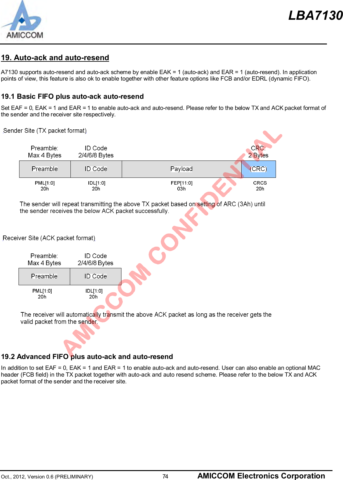
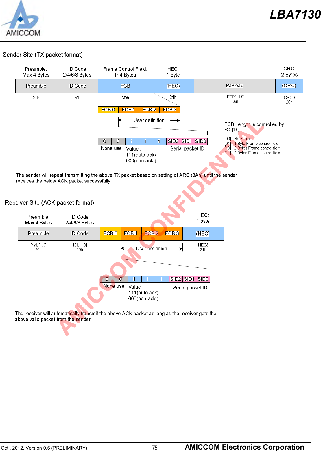
![LBA7130Oct., 2012, Version 0.6 (PRELIMINARY) 76 AMICCOM Electronics Corporation19.3 WTR Behavior during auto-ack and auto-resendIf auto-ack and auto-resend are enabled (EAR = EAK = 1), WTR represents a completed transmission period and CWTR is adebug signal which represents the cyclic TX period and cyclic RX period. Please refer to the below timing diagrams for details.The sender site (auto-resend)The receiver site (auto-ack)Remark: Refer to 3Bh for ARD[7:0] setting (auto resend delay).Refer to 3Fh for RND[7:0] setting (random seed for resend interval).Refer to 3Ah for EAK (enable auto-ack).Refer to 3Ah for EAR (enable auto-resend).Refer to 0Bh for VKM and VPM.](https://usermanual.wiki/LB-Technology/51402TR/User-Guide-1922627-Page-76.png)
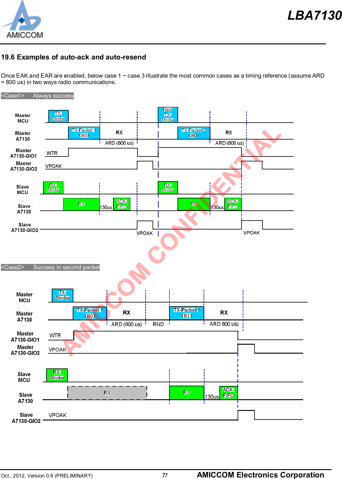
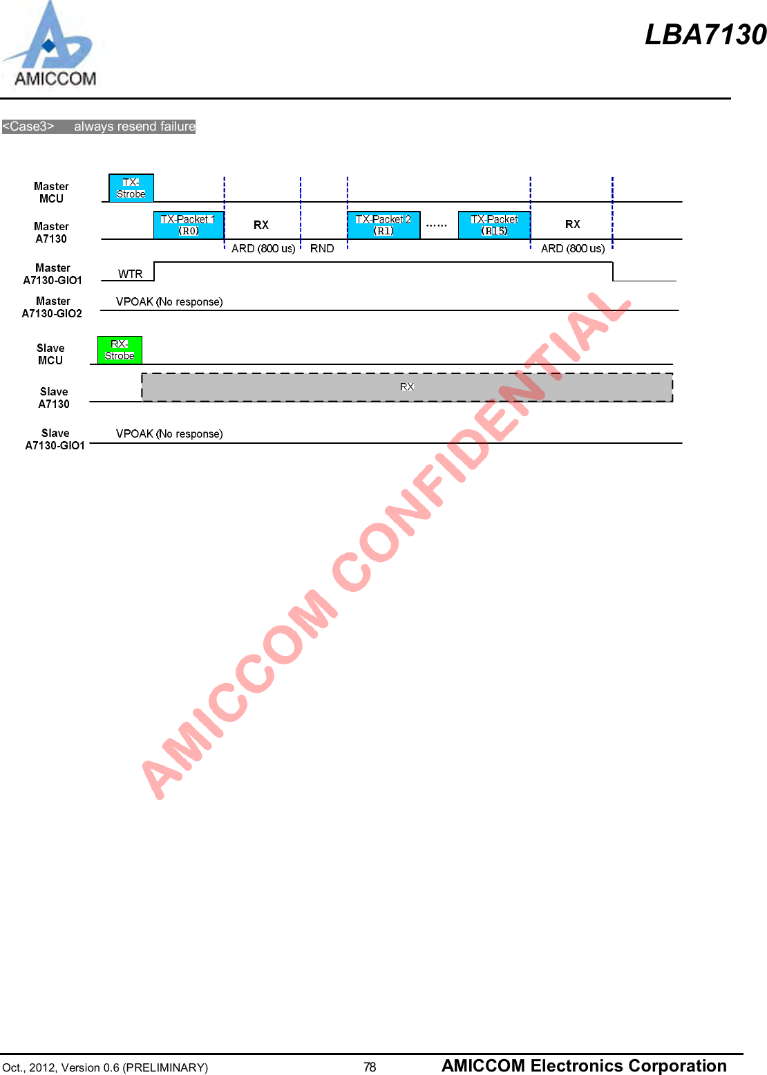
![LBA7130Oct., 2012, Version 0.6 (PRELIMINARY) 79 AMICCOM Electronics Corporation20. RC OscillatorA7130 has an internal RC oscillator to supports WOR (Wake On RX) and TWOR (Timer Wake On RX) function. RCOSC_E(09h) is used to enable RC oscillator. WORE (01h) is used to enable WOR function and TWORE (09h) is used to enable TWORfunction. After done calibrations of RC oscillator, WOR and TWOR function can be operated from -40℃ to 85℃.Parameter Min Max Unit NoteCalibrated Freq. 3.8K 4.2K HzSleep period 7.82 8007.68 ms [( WOR_SL [9:0] ) +1] x 7.8 msRX period 0.244 ms [( WOR_AC [5:0] ) +1] x 244 usOperation temperature -40 85 ℃After calibration.20.1 WOR FunctionWhen WOR is enabled (WORE = 1 and RCOSC_E =1), A7130 periodically wakes up f rom sleep and li sten (auto-enter RXmode) for incoming packets without MCU interaction. Therefore, A7130 will stay in sleep mode based on WOR_SL timer andRX mode based on WOR_AC timer unless a packet is received.The internal RC oscillator used for the WOR function varies with temperature and CMOS process deviation. In order to keep thefrequency as accurate as possible, the RC oscillator shall be calibrated (CALWC=1) whenever possible. After done calibrations,MCU shall set WORE=1 and issue sleep strobe command to start WOR function. After a period (WOR_SL) in sleep mode, thedevice goes to RX mode to check coming packets. And then, A7130 is back to sleep mode for the next WOR cycle. To end upWOR function, MCU just needs to set WORE = 0. Beware, please turn on MSCRC (21h, CRC data filtering) when CRCS = 1(20h, CRC select) in WOR function.Strobe CMD(SCS,SCK,SDIO) No Command RequiredsleepGIO1 -- WTR GIO1S[3:0]=0000RF In PinStrobecmdSleepWOR_SL[9:0]RX SleepWOT_SL[9:0]RXStart WOR(sleep strobe)ComingpacketEnd of WOR(set WORE = 0)](https://usermanual.wiki/LB-Technology/51402TR/User-Guide-1922627-Page-79.png)
![LBA7130Oct., 2012, Version 0.6 (PRELIMINARY) 80 AMICCOM Electronics Corporation20.2 TWOR FunctionThe RC oscillator inside A7130 can also be used to supports programmable TWOR (Timer Wake-On, TWORE=1) functionwhich enables A7130 to output a periodic square wave from GIO1 (or GIO2). The duty cycle of this square wave is set byWOR_AC (08h) or WOR_SL (08h and 07h) regarding to TSEL (09h). User can use this square wave to wake up MCU or otherpurposes.21. AES128 Security PacketA7130 has a built-in AES128 co-processor to generate a security packet by a general purpose MCU. In addition to support128-bits key length (AES128), A7130 also support a proprietary 32-bits key length called AES32.Software procedure to use AES128.Step1: Write 16-bytes AES128 key to KEYI [127:0] (36h)Step2: Set AESS=1 (3Eh) to select standard AES128Step3. Set AKFS=0 (3Eh) to disable attaching AES128 KEYI [127:0] into the TX packet.Step4: Set EDCRS=1 (3Eh) to enable AES co-processor.Step5: Write plain text to TX FIFOStep6: Issue TX strobe command and then A7130 will execute AES128 encryption and deliver the cipher text without latency.Step7: In RX side with the same configurations, A7130 will execute AES128 decryption and store plain text back to RX FIFO.Remark1. The unit size of AES128 encryption packet is 16-bytes.2. In TX side, if plain text is not dividable by 16-bytes, i.e. 5-bytes only, the TX packet is complement to be 16-bytes.3. In RX side, the coming cipher text will be decrypted and restore 5-bytes plain text back to RX FIFO.Software procedure to use AES32.Step1: Write 4-bytes AES128 key to KEYI [31:0] (36h)Step2: Set AESS=0 (3Eh) to select proprietary AES32.Step3. Set AKFS=0 (3Eh) to not attach AES128 KEYI [31:0] to the wanted TX packet.Step4: Set EDCRS=1 (3Eh) to enable AES co-processor.Step5: Write plain text to TX FIFOStep6: Issue TX strobe command and then A7130 will execute AES32 encryption and deliver the cipher text without latency.Step7: In RX side with the same configurations, A7130 will execute AES32 decryption and store plain text back to RX FIFO.Remark1. The unit size of AES32 encryption packet is 4-bytes.2. In TX side, if plain text is not dividable by 4-bytes, i.e. 5-bytes only, the TX packet is complement to 8-bytes.3. In RX side, the coming cipher text will be decrypted and restore 5-bytes plain text back to RX FIFO.](https://usermanual.wiki/LB-Technology/51402TR/User-Guide-1922627-Page-80.png)
![LBA7130Oct., 2012, Version 0.6 (PRELIMINARY) 81 AMICCOM Electronics Corporation22. Application circuit22.1 MD70-A01AMICCOM’s ref. design module, MD7130-A01, max 5 dBm output power, application circuit example.C1470pFSCSC2100pFC5100pFVDD_AC60.1uFR1NCSCKC9NCSDIOC82.2nFG I O1CKOG I O2G NDG NDVING NDC100.1uF12345678910J1CON/10P 2.012J2CON/2P 2.0C12NC12J3CON/2P 2.0C13NCC72.2uFSDIOSCKSCSVDD_ATP1ANTENNACKOGIO2GIO1V INC151.8pFANTC4 2.2uFL22.7nHC34.7uFVDD_AC11100pF 13G ND 2G ND4Y2 NC13G ND 2G ND4Y316M Hz XTA L_ 3. 2*2. 5Y1 NCBP_RSSI1BP_BG2RFI3RFC5RFO4V DD _ VCO6CP7VDD_PLL8XI9XO10GND 15SCS 11SCK 12SDIO 14VDD_D 13CKO 18GIO2 17GIO1 16REGI 19VDD_A 20A7130PKGU1A7130Remark1. RF Matching to 50Ω.2. RX and TX signal are combined internally to RFI pin only so that RFSP bit = 0 (DASP0 register = 0x34).3. Recommend 16MHz crystal with 18 pF Cload.4. Recommend to let C12 and C13 NC because of enabling on-chip Xtal Capacitors by (INTXC = 1 and CSXTAL = [10100]).](https://usermanual.wiki/LB-Technology/51402TR/User-Guide-1922627-Page-81.png)
![LBA7130Oct., 2012, Version 0.6 (PRELIMINARY) 82 AMICCOM Electronics Corporation22.2 MD70-F07AMICCOM’s ref. design module, MD7130-F07, typical 17 dBm output power together with a range extendor A7700.1 2 3 4ABCD4321DCBATitleNumbe r Revi si onSizeA4Dat e: 1 2- Ja n-2 012 S he et o fFile: C:\Docu ment s and Sett ings\ac008 6\桌面\MD7130~2.DDBDrawn By:MD7˄ˆ0-F07-05(2L)SCSSCKSDIOGIO1GIO2CKO or GNDGNDREGI33 12345678910J2CON/10P 2.0C2100pFVDD_AC29100pFR10NCC32NCC312.2nF C300.1uFC140.1uF 1 2Y116MHzC202.2uFSDIOSCKSCSC54.7uFVDD_ACKOGIO2GIO1R E GI 33C182.2uFVDD_ALNA_OUTPA_INC130.1uFC57100pFREGI33R66.8KREGI 33C36NCL23nHC3 8 NCC91.2pFTRXRFIRFOBGC338.2pFC25 1pFLNA_OUTPA_INC42NCREGI33VDD_PAC78.2pFL14.7nHC8NCANT2GND1VDD_PA4GND5VDD_BA7V DD _A8RFI 9RFO 11BG 13RX SW 15TX SW 14HGM 16NC3NC6GND 10BGS 12U2A7700TX SWRX SW2012.01.12C12.2pFL30RTP1TEST POINTC191.5pFC61.5pFC11NCL72.4nHL82.4nH R11 NCR12 0RCKOL9 3.3nHL10 3.3nHC101pFC161pFC31nFBP_RSSI1BP_ BG2RFI3RFC5RFO4VDD_VCO6CP7VDD_PLL8XI9XO10GND 15SCS 11SCK 12SDIO 14VDD_D 13CKO 18GIO2 17GIO1 16RE GI 19VDD_A 20A7130 PKGU1A70TX SWRX SWC12NCC15NCC34NC C37NC1 2Y2 16MHz13GND 2GND4Y3CRYSTAL/5*3.2R147Remark1. RF matching to 50Ω.2. RX and TX signal are separated to RFI pin and RFO pin so that RFSP bit = 1 (DASP0 register = 0x74).3. Recommend 16MHz crystal with 18 pF Cload.4. Recommend to let C34 and C37 NC because of enabling on-chip Xtal Capacitors by (INTXC = 1 and CSXTAL = [10100]).](https://usermanual.wiki/LB-Technology/51402TR/User-Guide-1922627-Page-82.png)