LB Technology 51402TR LBA 7130RF User Manual Title
LB Technology Co., Ltd. LBA 7130RF Title
User manual

LBA7130
Oct., 2012, Version 0.6 (PRELIMINARY) 1 AMICCOM Electronics Corporation
Document Title
A7130 Data Sheet, 2.4GHz FSK/GFSK Transceiver with 4Mbps data rate
Revision History
Rev. No. History Issue Date Remark
0.0 Initial issue. Dec, 2009 Objective
0.1 Update ch8 and the application circuit. July, 2011 Preliminary,
0.2 Modify the tape reel information and the add Shenzhen office
address.
July, 2011 Preliminary,
0.3 Add Ch20 WOR and Ch21 AES128. Aug., 2011 Preliminary,
0.4 Add section 16.4.3 FIFO extension and Ch21 AES128.
Update sleep cur rent, Xtal start up time and PDL formula, TMOE
timing, WTR Timing, and Ch14.
Apr., 2012 Preliminary,,
0.5 Remove 3Mbps data rate
Add descriptions for HECF, FECF and CRCF clear method in 9.2.1
Aug.,2012 Preliminary
0.6 Add suggestion in WOR function Oct. 2012 Preliminary
Important Notice:
AMICCOM r eserves t he right t o make changes t o its products or to discontinue any integrated circuit prod uct or se rvice
without notice. AMICCOM integrated circuit products are not designed, intended, authorized, or warranted to be suitable for
use in life-support a pplications, de vices o r sys tems or ot her critical ap plications. Use of AM ICCOM products in such
applications is understood to be fully at the risk of the customer.

LBA7130
Oct., 2012, Version 0.6 (PRELIMINARY) 2 AMICCOM Electronics Corporation
Table of Contents
1. General Description....................................................................................................................................................... 5
2. Typical Applications ....................................................................................................................................................... 5
3. Feature ......................................................................................................................................................................... 5
4. Pin Configurations ......................................................................................................................................................... 6
5. Pin Description (I: input; O: output, I/O: input or output)................................................................................................... 7
6. Chip Block Diagram....................................................................................................................................................... 8
7. Absolute Maximum Ratings............................................................................................................................................ 9
8. Electrical Specification..................................................................................................................................................10
9. Control Register ...........................................................................................................................................................12
9.1 Control register table............................................................................................................................................12
9.2 Control register description ..................................................................................................................................15
9.2.1 Mode Register (Address: 00h)....................................................................................................................15
9.2.2 Mode Control Register (Address: 01h)......................................................................................................15
9.2.3 Calibration Control Register (Address: 02h)..............................................................................................16
9.2.4 FIFO Register I (Address: 03h).................................................................................................................16
9.2.5 FIFO Register II (Address: 04h)................................................................................................................16
9.2.6 FIFO DATA Register (Address: 05h) .........................................................................................................16
9.2.7 ID DATA Register (Address: 06h)................................................................................................................16
9.2.8 RC OSC Register I (Address: 07h) .............................................................................................................17
9.2.9 RC OSC Register II (Address: 08h).............................................................................................................17
9.2.10 RC OSC Register III (Address: 09h)..........................................................................................................17
9.2.11 CKO Pin Control Register (Address: 0Ah) .................................................................................................17
9.2.12 GIO1 Pin Control Register I (Address: 0Bh)...............................................................................................18
9.2.13 GIO2 Pin Control Register II (Address: 0Ch) .............................................................................................20
9.2.14 Clock Register (Address: 0Dh)..................................................................................................................21
9.2.15 PLL Register I (Address: 0Eh)...................................................................................................................21
9.2.16 PLL Register II (Address: 0Fh)..................................................................................................................21
9.2.17 PLL Register III (Address: 10h).................................................................................................................22
9.2.18 PLL Register IV (Address: 11h).................................................................................................................22
9.2.19 PLL Register V (Address: 12h) ...............................................................................................................22
9.2.20 Channel Group Register I (Address: 13h)..................................................................................................22
9.2.21 Channel Group Register II (Address: 14h).................................................................................................22
9.2.22 TX Register I (Address: 15h).....................................................................................................................23
9.2.23 TX Register II (Address: 16h)....................................................................................................................23
9.2.24 Delay Register I (Address: 17h)................................................................................................................23
9.2.25 Delay Register II (Address: 18h) ...............................................................................................................24
9.2.26 RX Register (Address: 19h)......................................................................................................................24
9.2.27 RX Gain Register I (Address: 1Ah)............................................................................................................25
9.2.28 RX Gain Register II (Address: 1Bh)...........................................................................................................25
9.2.29 RX Gain Register III (Address: 1Ch) .........................................................................................................25
9.2.30 RX Gain Register IV (Address: 1Dh).........................................................................................................26
9.2.31 RSSI Threshold Register (Address: 1Eh) ..................................................................................................26
9.2.32 ADC Control Register (Address: 1Fh)........................................................................................................26
9.2.33 Code Register I (Address: 20h).................................................................................................................26
9.2.34 Code Register II (Address: 21h)................................................................................................................27
9.2.35 Code Register III (Address: 22h)...............................................................................................................27
9.2.36 IF Calibration Register I (Address: 23h).....................................................................................................27
9.2.37 IF Calibration Register II (Address: 24h)....................................................................................................28
9.2.38 VCO current Calibration Register (Address: 25h).......................................................................................28
9.2.39 VCO band Calibration Register I (Address: 26h)........................................................................................28
9.2.40 VCO band Calibration Register II (Address: 27h).......................................................................................29
9.2.41 VCO Deviation Calibration Register I (Address: 28h) .................................................................................29
9.2.42 VCO Deviation Calibration Register II (Address: 29h) ................................................................................29
9.2.43 DASP0 (Address: 2Ah, Page 0 by AGT [3:0]=0) ........................................................................................30
9.2.43 DASP1 (Address: 2Ah, Page 1 by AGT[3:0]=1) .........................................................................................30

LBA7130
Oct., 2012, Version 0.6 (PRELIMINARY) 3 AMICCOM Electronics Corporation
9.2.43 DASP2 (Address: 2Ah, Page 2 by AGT[3:0]=2) .........................................................................................30
9.2.43 DASP3 (Address: 2Ah, Page 3 by AGT[3:0]=3) .........................................................................................31
9.2.43 DASP4 (Address: 2Ah, Page 4 by AGT[3:0]=4) .........................................................................................31
9.2.43 DASP5 (Address: 2Ah, Page 5 by AGT[3:0]=5) .........................................................................................31
9.2.43 DASP6 (Address: 2Ah, Page 6 by AGT[3:0]=6) .........................................................................................31
9.2.43 DASP7 (Address: 2Ah, Page 7 by AGT[3:0]=7) .........................................................................................31
9.2.44 VCO Modulation Delay Register (Address: 2Bh)........................................................................................31
9.2.45 Battery detect Register (Address: 2Ch).....................................................................................................32
9.2.46 TX test Register (Address: 2Dh) ...............................................................................................................32
9.2.47 Rx DEM test Register I (Address: 2Eh) .....................................................................................................32
9.2.48 Rx DEM test Register II (Address: 2Fh).....................................................................................................33
9.2.49 Charge Pump Current Register I (Address: 30h) .......................................................................................33
9.2.50 Charge Pump Current Register II (Address: 31h).......................................................................................33
9.2.51 Crystal test Register (Address: 32h)..........................................................................................................33
9.2.52 PLL test Register (Address:33h) ...............................................................................................................34
9.2.53 VCO test Register I (Address:34h)............................................................................................................34
9.2.54 RF Analog Test Register (Address: 35h)....................................................................................................34
9.2.55 AES Key data Register (Address: 36h)......................................................................................................35
9.2.56 Channel Select Register (Address: 37h)....................................................................................................35
9.2.57 ROMP0 (Address: 38h, Page 0 by AGT[3:0]=0).........................................................................................35
9.2.57 ROMP1 (Address: 38h, Page 1 by AGT[3:0]=1).........................................................................................35
9.2.57 ROMP2 (Address: 38h, Page 2 by AGT[3:0]=2).........................................................................................36
9.2.57 ROMP3 (Address: 38h, Page 3 by AGT[3:0]=3).........................................................................................36
9.2.57 ROMP4 (Address: 38h, Page 4 by AGT[3:0]=4).........................................................................................36
9.2.58 Data Rate Clock Register (Address: 39h)..................................................................................................36
9.2.59 FCR Register (Address: 3Ah) ...................................................................................................................36
9.2.60 ARD Register (Address: 3Bh) ...................................................................................................................37
9.2.61 AFEP Register (Address: 3Ch)..................................................................................................................37
9.2.62 FCB Register (Address: 3Dh) ...................................................................................................................37
9.2.63 KEYC Register (Address: 3Eh).................................................................................................................38
9.2.64 USID Register (Address: 3Fh) ..................................................................................................................38
10. SPI.............................................................................................................................................................................39
10.1 SPI Format ........................................................................................................................................................40
10.2 SPI Timing Characteristic ...................................................................................................................................40
10.3 SPI Timing Chart................................................................................................................................................41
10.3.1 Timing Chart of 3-wire SPI........................................................................................................................41
10.3.2 Timing Chart of 4-wire SPI........................................................................................................................41
10.4 Strobe Commands .............................................................................................................................................42
10.4.1 Strobe Command - Sleep Mode................................................................................................................42
10.4.2 Strobe Command - ldle Mode ...................................................................................................................42
10.4.3 Strobe Command - Standby Mode ............................................................................................................43
10.4.4 Strobe Command - PLL Mode...................................................................................................................43
10.4.5 Strobe Command - RX Mode....................................................................................................................44
10.4.6 Strobe Command - TX Mode ....................................................................................................................44
10.4.7 Strobe Command – FIFO Write Pointer Reset ...........................................................................................44
10.4.8 Strobe Command – FIFO Read Pointer Reset ...........................................................................................45
10.4.9 Strobe Command – Deep Sleep Mode......................................................................................................45
10.5 Reset Command................................................................................................................................................46
10.6 ID Accessing Command.....................................................................................................................................46
10.6.1 ID Write Command...................................................................................................................................46
10.6.2 ID Read Command ..................................................................................................................................47
10.7 FIFO Accessing Command.................................................................................................................................47
10.7.1 TX FIFO Write Command.........................................................................................................................47
10.7.2 Rx FIFO Read Command.........................................................................................................................48
11. State machine.............................................................................................................................................................49
11.1 Key states..........................................................................................................................................................49
11.2 FIFO mode ........................................................................................................................................................50
11.3 Direct mode .......................................................................................................................................................51
12. Crystal Oscillator ........................................................................................................................................................54
12.1 Use External Crystal ..........................................................................................................................................54

LBA7130
Oct., 2012, Version 0.6 (PRELIMINARY) 4 AMICCOM Electronics Corporation
12.2 Use External Clock ............................................................................................................................................54
13. System Clock .............................................................................................................................................................55
13.2 Data Rate Setting ..............................................................................................................................................55
14. Transceiver LO Frequency..........................................................................................................................................56
14.1 LO Frequency Setting........................................................................................................................................56
14.2 IF Side Band Select ...........................................................................................................................................57
14.2.1 Auto IF Exchange.....................................................................................................................................58
14.2.2 Fast Exchange.........................................................................................................................................59
14.3 Auto Frequency Compensation...........................................................................................................................60
15. Calibration..................................................................................................................................................................60
15.1 Calibration Procedure ........................................................................................................................................60
16. FIFO (First In First Out)...............................................................................................................................................61
16.1 TX Packet Format in FIFO mode........................................................................................................................61
16.1.1 Basic FIFO mode.....................................................................................................................................61
16.1.2 Advanced FIFO mode...............................................................................................................................61
16.2 Bit Stream Process in FIFO mode.......................................................................................................................62
16.3 Transmission Time.............................................................................................................................................63
16.4 Usage of TX and RX FIFO .................................................................................................................................63
16.4.1 Easy FIFO ...............................................................................................................................................64
16.4.2 Segment FIFO .........................................................................................................................................65
16.4.3 FIFO Extension........................................................................................................................................67
17. ADC (Analog to Digital Converter) ...............................................................................................................................71
17.1 RSSI Measurement............................................................................................................................................71
18. Battery Detect ............................................................................................................................................................73
19. Auto-ack and auto-resend...........................................................................................................................................74
19.1 Basic FIFO plus auto-ack auto-resend................................................................................................................74
19.2 Advanced FIFO plus auto-ack and auto-resend...................................................................................................74
19.3 WTR Behavior during auto-ack and auto-resend.................................................................................................76
19.6 Examples of auto-ack and auto-resend...............................................................................................................77
20. RC Oscillator..............................................................................................................................................................79
20.1 WOR Function...................................................................................................................................................79
20.2 TWOR Function.................................................................................................................................................80
21. AES128 Security Packet .............................................................................................................................................80
22. Application circuit........................................................................................................................................................81
22.1 MD7130-A01 .....................................................................................................................................................81
22.2 MD7130-F07 .....................................................................................................................................................82
23. Abbreviations..............................................................................................................................................................83
24. Ordering Information...................................................................................................................................................83
25. Package Information...................................................................................................................................................84
26. Top Marking Information..............................................................................................................................................85
27. Reflow Profile.............................................................................................................................................................86
28. Tape Reel Information.................................................................................................................................................87
29. Product Status............................................................................................................................................................89

LBA7130
Oct., 2012, Version 0.6 (PRELIMINARY) 5 AMICCOM Electronics Corporation
1. General Description
A7130 is a high performance and low cost 2.4GHz ISM band wireless transceiver. This device integrates both high sensitivity
receiver (- 88dBm @4Mbps) and programmable power amplifier 5dBm. Based on Data Rate Register (39h), user can
configure on-air data rates to 4Mbps.
A7130 supports fast settling time (90 us) for frequency hopping system. For packet handling, A7130 has built-in separated
64-bytes TX/ RX FIFO (could be logically extended t o 4K b ytes) for da ta buffering and bu rst trans mission, aut o-ack a nd
auto-resend, CRC for error packet filtering, FEC for 1-bit data correction per code word, RSSI for clear channel assessment,
thermal sensor f or m onitoring r elative t emperature, WOR (Wake o n RX) f unction to s upport periodically wake up from sleep
mode to RX mode and listen for incoming packets without MCU interaction, data whitening for data encryption / decryption. In
addition, A7130 ha s bu ilt-in AES128 co -processor (Adva nced Encr yption St andard) for advan ced dat a e ncryption and
decryption which consists of the transformation of a 128-bit block into an encrypted 128-bit block. Those functions are very
easy to use while developing a wireless system. All features are integrated in a small QFN 4X4 20 pins package.
A7130’s control registers ar e a ccessed via 3- wire o r 4-wire S PI interface s uch as TX/RF FIFO, ID r egister, RSSI value,
frequency hopping to chip calibration procedures. Another one, via SPI as well, is the unique Strobe command, A7130 can
be cont rolled from power sav ing mode (deep s leep, sl eep, idle , standby ), PLL mode, TX mode and R X mode. The other
connections between A7130 and MCU are GIO1 and GIO2 (multi-function GPIO) to output A7130’s status so that MCU could
use either polling or int errupt scheme for radio cont rol. Overall, this de vice is ve ry easy-to-use for de veloping a w ireless
application with a MCU.
2. Typical Applications
n 2.4GHz video baby monitor
n 2.4GHz PC peripherals
n HiFi quality wireless audio streaming
n 2408 ~ 2468 MHz ISM system
n Wireless metering and building automation
n Wireless toys and game controllers
3. Feature
n Small size (QFN4 X4, 20 pins).
n Frequency band: 2408 ~ 2468MHz.
n FSK or GFSK modulation
n Low current consumption: RX 27mA (4Mbps), TX 29mA (at 5dBm output power).
n Deep sleep current (0.1 uA).
n Sleep current (2.5 uA).
n On chip regulator, support input voltage 2.0 ~ 3.6 V.
n Data rate 4Mbps.
n Programmable TX power level from 5 dBm.
n Ultra High sensitivity:
u -88dBm at 4Mbps on-air data rate.
n Fast settling time (90 us) synthesizer for frequency hopping system.
n On chip low power RC oscillator for WOR (Wake on RX) function.
n Built-in AES128 co-processor
n AGC (Auto Gain Control) for the wide RSSI dynamic range.
n AFC (Auto Frequency Compensation) for frequency drift due to temperature.
n Support low cost crystal (16 / 18 MHz).
n Low Battery Detector indication.
n Easy to use.
u Support 3-wire or 4-wire SPI.
u Unique Strobe command via SPI.
u ONE register setting for new channel frequency.
u CRC Error Packet Filtering.
u Auto-acknowledgement and auto-resend.
u Dynamic FIFO length.
u 8-bits RSSI measurement for clear channel indication.
u Auto Calibrations.

LBA7130
Oct., 2012, Version 0.6 (PRELIMINARY) 6 AMICCOM Electronics Corporation
u Auto IF function.
u Auto FEC by (7, 4) Hamming code (1 bit error correction / code word).
u Separated 64 bytes RX and TX FIFO.
u Easy FIFO / Segment FIFO / FIFO Extension (up to 4K bytes).
u Support FIFO mode frame sync to MCU.
u Support direct mode with recovery clock output to MCU.
4. Pin Configurations
13
11
1
2
3
4
5
VDD_D
15
14
12
20
19
18
17
16
6
7
8
9
10
SDIO
SCS
BP_BG
RFI
RSSI
RFO
RFC
GIO1
GIO2
CKO
V_VCO
CP
XO
V_PLL
XI
SCK
GND
REGI
VDD_A
Fig 4-1. A7130 QFN 4x4 Package Top View
LBA7130
Oct., 2012, Version 0.6 (PRELIMINARY) 7 AMICCOM Electronics Corporation
5. Pin Description (I: input; O: output, I/O: input or output)
Pin No. Symbol I/O Function Description
1RSSI O Connected to a bypass capacitor for RSSI.
2BP_BG O Connected to a bypass capacitor for internal Regulator bias point.
3RFI I LNA input. Connected to matching circuit.
4RFO O PA input. Connected to matching circuit.
5RFC I RF Choke input. Connected to matching circuit.
6V_VCO I VCO supply voltage input.
7CP O Charge-pump. Connected to loop filter.
8 V_PLL I PLL supply voltage input.
9XI I Crystal oscillator input.
10 XO O Crystal oscillator output.
11 SCS I SPI chip select.
12 SCK I SPI clock input pin.
13 VDD_D I Connected to a bypass capacitor to supply voltage for digital part.
14 SDIO I/O SPI read/write data.
15 GND G G round
16 GIO1 I/O Multi-function GIO1 / 4-wire SPI data output.
17 GIO2 I/O Multi-function GIO2 / 4-wire SPI data output.
18 CKO O Multi-function clock output.
19 REGI I Regulator input (External Power Input)
20 VDD_A O Internal Regulator output to supply V_VCO (pin 6), V_PLL (pin 8) and RFC (pin 5).
Back side plate GGround.
Back side plate shall be well-solder to ground; otherwise, it will impact RF performance.
LBA7130
Oct., 2012, Version 0.6 (PRELIMINARY) 8 AMICCOM Electronics Corporation
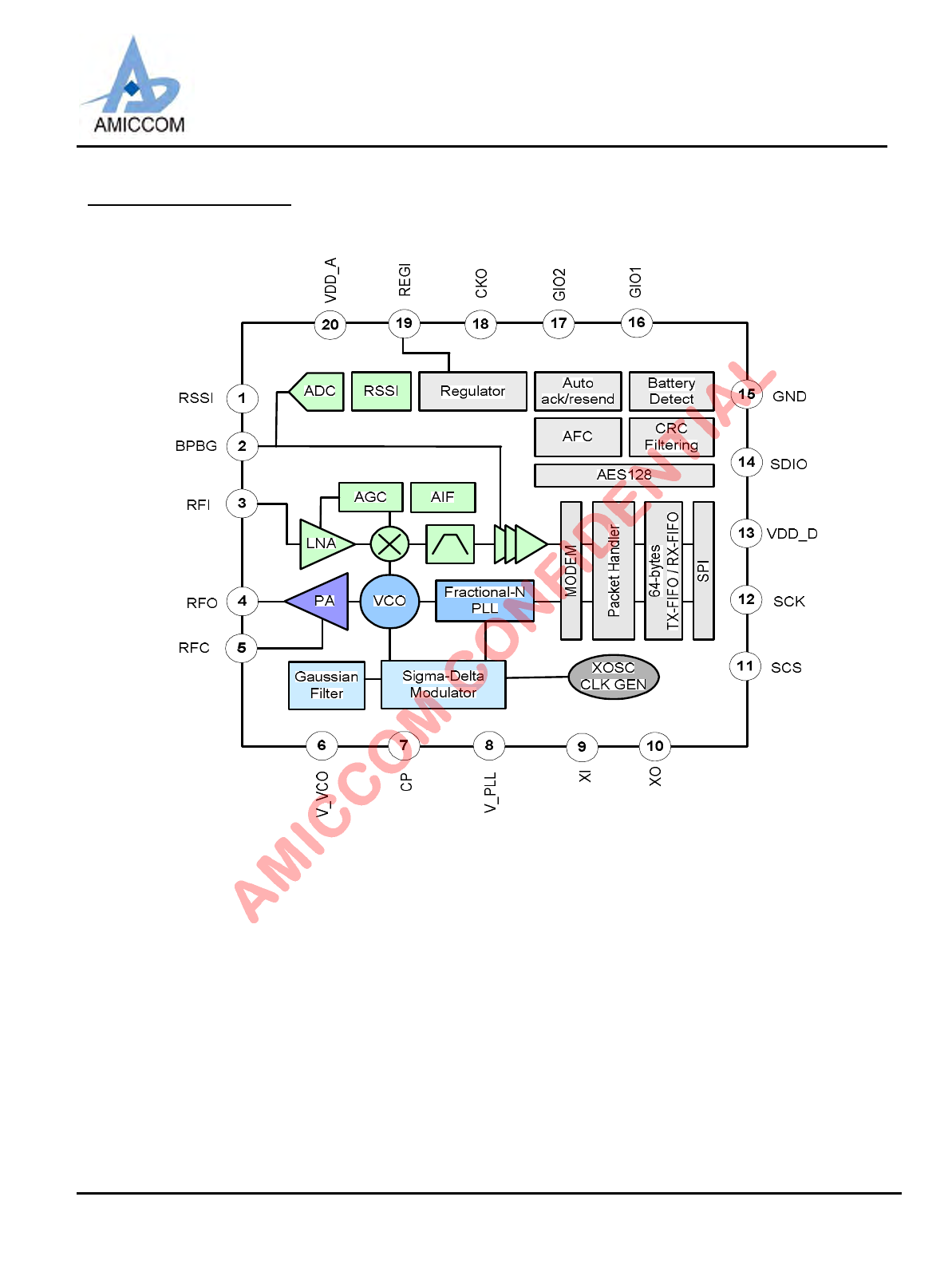
6. Chip Block Diagram
Fig 6-1. A7130 Block Diagram
LBA7130
Oct., 2012, Version 0.6 (PRELIMINARY) 9 AMICCOM Electronics Corporation
7. Absolute Maximum Ratings
Parameter With respect to Rating Unit
Supply voltage range (VDD) GND -0.3 ~ 3.6 V
Digital IO pins range GND -0.3 ~ VDD+0.3 V
Voltage on the analog pins range GND -0.3 ~ 2.1 V
Input RF level 10 dBm
Storage Temperature range -55 ~ 125 °C
HBM ± 2K VESD Rating
MM ± 100 V
*Stresses above those listed under “ Absolute Maximum Rating” may cause permanent damage to the device. These are
stress ratings only; functional operation of the device at these or any other conditions above those indicated in the operational
sections of this specification is not implied. Exposure to absolute-maximum-rated conditions for extended periods may affect
device reliability.
*Device is ESD sensitive. Use appropriate ESD precautions. HBM (Human Body Mode) is tested under MIL-STD-883F
Method 3015.7. MM (Machine Mode) is tested under JEDEC EIA/JESD22-A115-A.
*Device is Moisture Sensitivity Level III (MSL 3).
LBA7130
Oct., 2012, Version 0.6 (PRELIMINARY) 10 AMICCOM Electronics Corporation
8. Electrical Specification
(Ta=25℃,VDD=3.3V, FXTAL =16MHz, with Match circuit and low pass filter, On Chip Regulator = 1.8V, unless otherwise noted.)
Parameter Description Min. Type Max. Unit
General
Operating Temperature -40 85 °C
Supply Voltage (VDD) with internal regulator 2.0 3.3 3.6 V
Current Consumption Deep Sleep mode*1
(No registers retention)
0.1 mA
Sleep mode (WOR off) *12.5 mA
Sleep mode (WOR on) *13.5 mA
Idle Mode (Regulator on) *10.3 mA
Standby Mode
(XOSC on, CLK Gen. on)
2.7 mA
PLL mode 12.5 mA
RX Mode (4Mbps) 27 mA
TX Mode (5dBm) 29 mA
TX Mode (3dBm) 24 mA
TX Mode (0dBm) 20 mA
TX Mode ( -5dBm) 18 mA
Current Consumption
(DBL =0 at 0Fh, bit7)
TX Mode ( -17dBm) 16 mA
PLL block
Idle to standby
(Xtal osc. is stable at 20ppm)
1ms
Crystal start up time*2
(3225 SMD type)
Idle to standby
(Xtal osc. is stable at 10ppm)
2ms
Crystal frequency Data rate: 4Mbps 16 MHz
Crystal tolerance Data rate: 4M/bps ±50 ppm
Crystal ESR 80 ohm
VCO Operation Frequency 24082468 MHz
PLL phase noise Offset 10k
Offset 500K
Offset 1M
75
90
100
dBc
PLL settling time*3Loop filter based on app. circuit.
(Standby to PLL)
30 mS
Transmitter
Output power range -17 0 5 dBm
30MHz~1GHz -36 dBm
1GHz~12.75GHz -30 dBm
1.8GHz~ 1.9GHz -47 dBm
Out Band Spurious Emission *4
5.15GHz~ 5.3GHz -47 dBm
Frequency deviation*5Data rate 4Mbps ±1M Hz
Data rate 4M bps
TX ready time*6Standby to TX 90 mS
Receiver
Data rate 4Mbps -88Receiver sensitivity
@ BER = 0.1% Data rate 4Mbps (GFSK) -85
dBm
LBA7130
Oct., 2012, Version 0.6 (PRELIMINARY) 11 AMICCOM Electronics Corporation
IF Filter bandwidth IFS = [11], 4Mbps 4.8M Hz
IF center frequency IFS = [11], 4Mbps 4M Hz
Co-Channel (C/I0) 11 dB
±4MHz Adjacent Channel 0 dB
±8MHz Adjacent Channel - 10 dB
±12MHz Adjacent Channel - 20 dB
±16MHz Adjacent Channel - 30 dB
Interference *7
(4Mbps , IF = 4MHz)
Image (C/IIM)- 10 dB
Maximum Operating Input Power @RF input (BER=0.1%) 5 dBm
30MHz~1GHz -57 dBm
RX Spurious Emission *4
1GHz~12.75GHz -47
AGC = 0 -95 -50 dBmRSSI Range
AGC = 1 -95 -20 dBm
RX Ready Time 80 ms
Regulator
Regulator settling time Pin 2 connected to 470pF.
(Sleep to idle).
0.5 ms
Band-gap reference voltage 1.28 V
Regulator output voltage 1.79 1.8 2.3 V
Digital IO DC characteristics
High Level Input Voltage (VIH)0.8*VDD VDD V
Low Level Input Voltage (VIL) 0 0.2*VDD V
High Level Output Voltage (VOH)@IOH= -0.5mA VDD-0.4 VDD V
Low Level Output Voltage (VOL)@IOL= 0.5mA 0 0.4 V
Note 1: When digital I/O pins are configured as input, those pins shall NOT be floating but pull either high or low (SCS shall
be pulled high only); otherwise, leakage current will be induced.
Note 2: Xtal settling time is depend on Xtal package type, Xtal ESR and Xtal Cm.
Note 3: Refer to Delay Register I (17h) to set PDL (PLL settling delay).
Note 4: With external RF filter that provides minimum 17dB of attenuation in the band: 30MHz ~ 2GHz and 3GHz ~12.75GHz.
Note 5: Refer to TX Register II (16h) to set FD [7:0].
Note 6: Refer to Delay Register I (17h) to set PDL and TDL.
Note 7: The wanted signal is set above sensitivity level +3dB. The modulation data of wanted signal and interferer
are PN9 and PN15, respectively.
LBA7130
Oct., 2012, Version 0.6 (PRELIMINARY) 12 AMICCOM Electronics Corporation
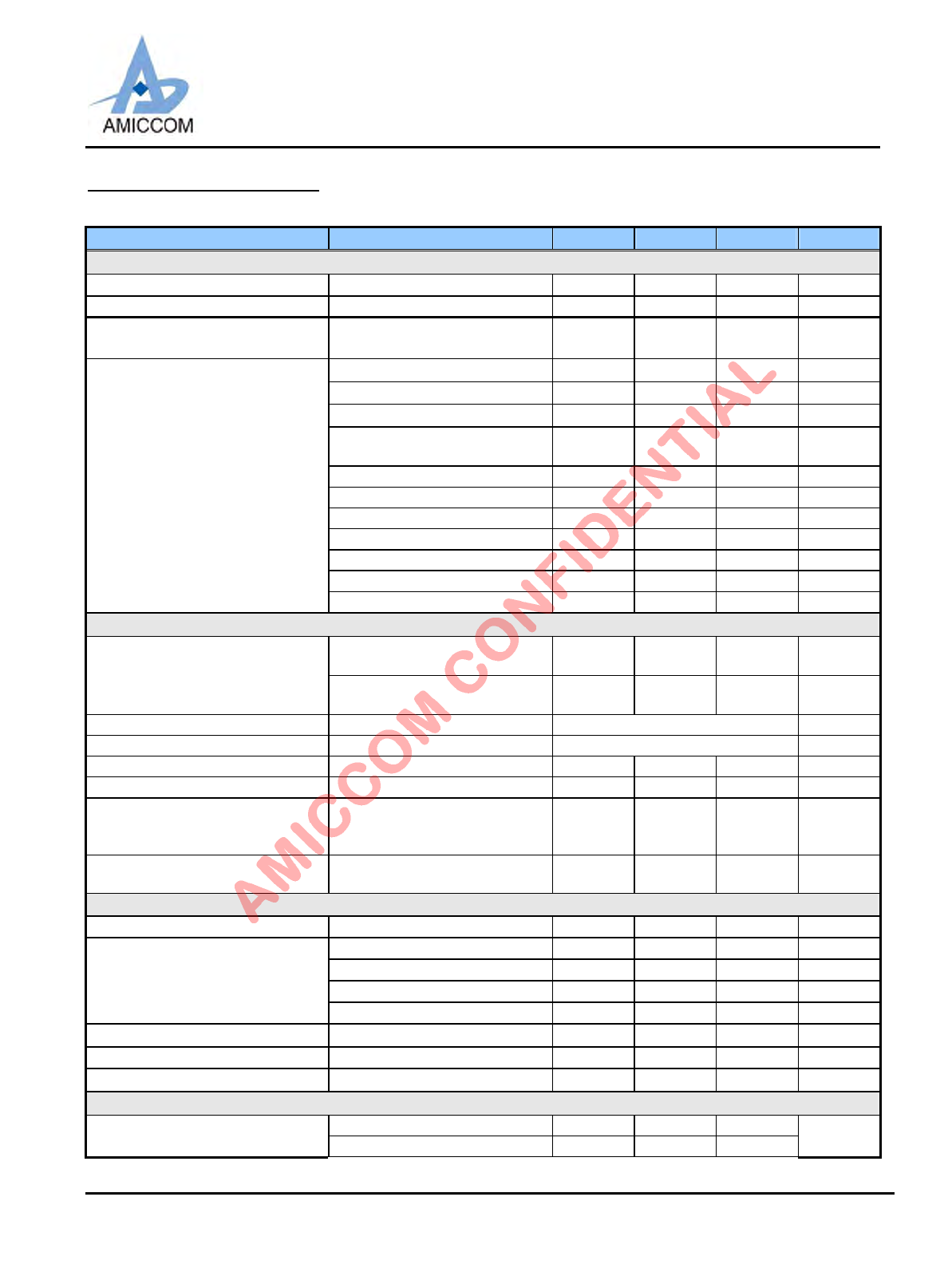
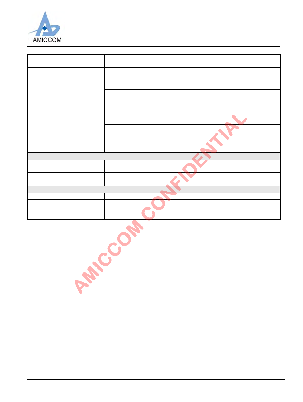
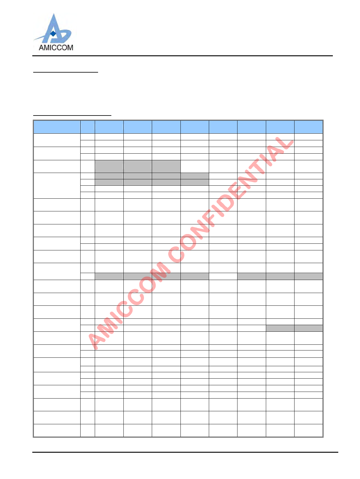
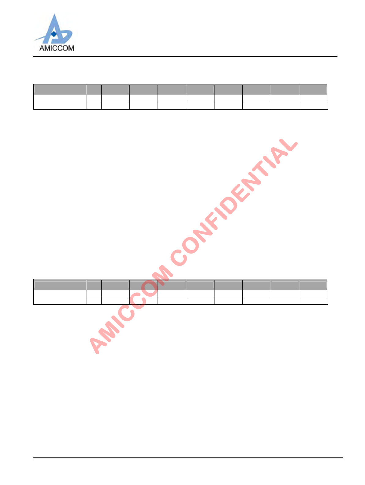
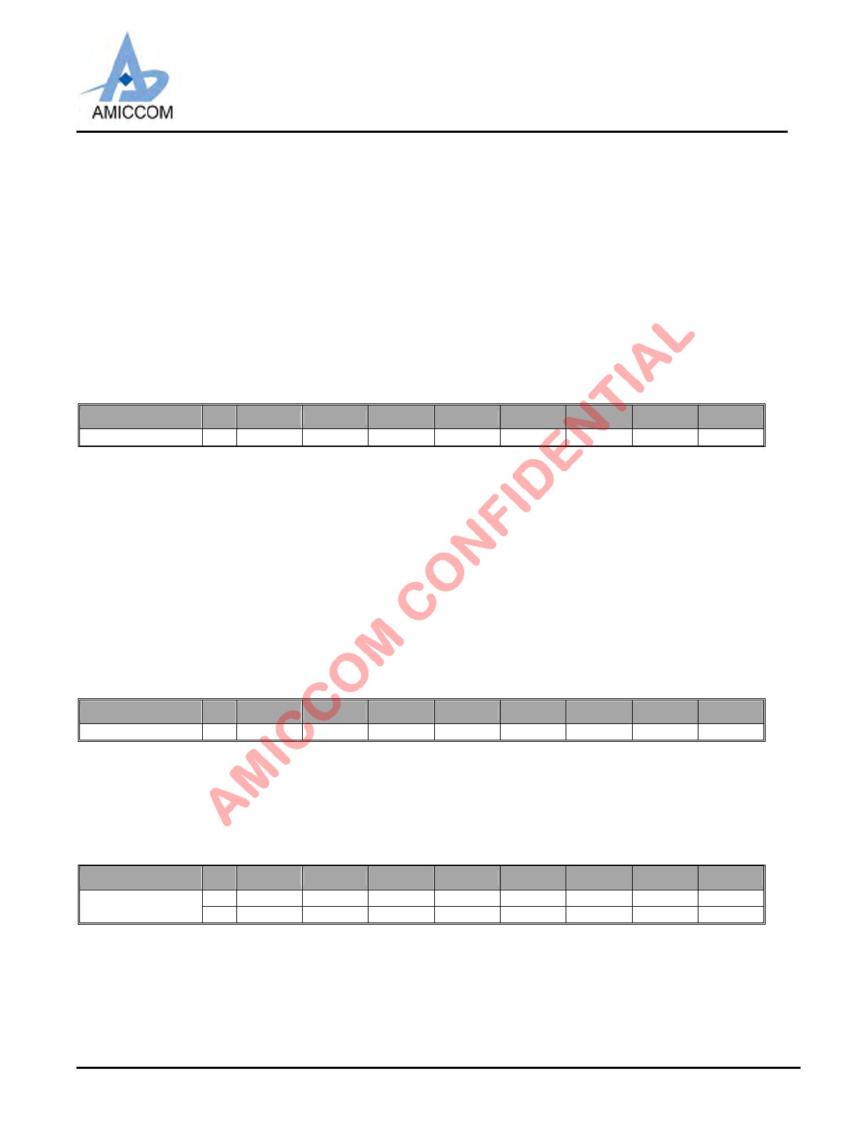
9. Control Register
A7130 contains 69 control registers. MCU can access those control registers via 3-wire (SCS, SCK, SDIO) or 4-wire (SCS,
SCK, SDIO, GIO1/GIO2) SPI interface (max. 15 Mbps). Please refer to Chapter 10 for SPI timing. In general, most of control
registers are just need to configure the recommended values based on A7130 reference code.
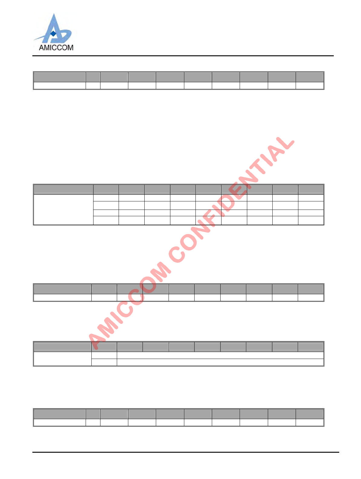
9.1 Control register table
Address /
Name R/W Bit 7 Bit 6 Bit 5 Bit 4 Bit 3 Bit 2 Bit 1 Bit 0
WRESETN RESETN RESETN RESETN RESETN RESETN RESETN RESETN00h
Mode RHECF FECF CRCF CER XER PLLER TRSR TRER
WDDPC ARSSI AIF DFCD WORE FMT FMS ADCM
01h
Mode control RDDPC ARSSI AIF CD WORE FMT FMS ADCM
02h
Calc R/W -- -- -- VCC VBC VDC FBC RSSC
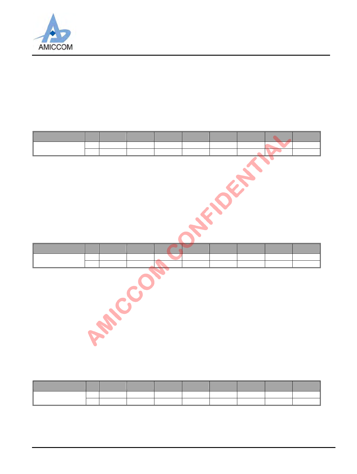
W-- -- -- -- FEP11 FEP10 FEP9 FEP8
R-- -- -- -- LENF11 LENF10 LENF9 LENF8
WFEP7 FEP6 FEP5 FEP4 FEP3 FEP2 FEP1 FEP0
03h
FIFO I
RLENF7 LENF6 LENF5 LENF4 LENF3 LENF2 LENF1 LENF0
04h
FIFO II WFPM1 FPM0 PSA5 PSA4 PSA3 PSA2 PSA1 PSA0
05h
FIFO Data R/W FIFO7 FIFO6 FIFO5 FIFO4 FIFO3 FIFO2 FIFO1 FIFO0
06h
ID Data R/W ID7 ID6 ID5 ID4 ID3 ID2 ID1 ID0
WWOR_SL7 WOR_SL6 WOR_SL5 WOR_SL4 WOR_SL3 WOR_SL2 WOR_SL1 WOR_SL0
07h
RC OSC I RRCOC7 RCOC6 RCOC5 RCOC4 RCOC3 RCOC2 RCOC1 RCOC0
08h
RC OSC II WWOR_SL9 WOR_SL8 WOR_AC5 WOR_AC4 WOR_AC3 WOR_AC2 WOR_AC1 WOR_AC0
WRTCS RCOT2 RCOT1/
RTCC1
RCOT0/
RTCC0 CALWC RCOSC_E TSEL TWORE
09h
RC OSC III R-- -- -- -- CALWR -- -- --
0Ah
CKO Pin WECKOE CKOS3 CKOS2 CKOS1 CKOS0 CKOI CKOE SCKI
0Bh
GPIO1 Pin I WVKM VPM GIO1S3 GIO1S2 GIO1S1 GIO1S0 GIO1I GIO1OE
0Ch
GPIO2 Pin II WBBCKS1 BBCKS0 GIO2S3 GIO2S2 GIO2S1 GIO2S0 GIO2I GIO2OE
WCGC1 CGC0 GRC3 GRC2 GRC1 GRC0 CGS XS
0Dh
Clock RIFS1 IFS0 GRC3 GRC2 GRC1 GRC0 -- --
0Eh
PLL I R/W CHN7 CHN6 CHN5 CHN4 CHN3 CHN2 CHN1 CHN0
WDBL RRC1 RRC0 CHR3 CHR2 CHR1 CHR0 BIP8
0Fh
PLL II RDBL RRC1 RRC0 CHR3 CHR2 CHR1 CHR0 IP8
WBIP7 BIP6 BIP5 BIP4 BIP3 BIP2 BIP1 BIP0
10h
PLL III RIP7 IP6 IP5 IP4 IP3 IP2 IP1 IP0
WBFP15 BFP14 BFP13 BFP12 BFP11 BFP10 BFP9 BFP8
11h
PLL IV R FS YN-FP15 AC14-FP14 AC13-FP13 AC12-FP12 AC11-FP11 AC10-FP10 AC9-FP9 AC8-FP8
WBFP7 BFP6 BFP5 BFP4 BFP3 BFP2 BFP1 BFP0
12h
PLL V RAC7-FP7 AC6-FP6 AC5-FP5 AC4-FP4 AC3-FP3 AC2-FP2 AC1-FP1 AC0-FP0
13h
Channel Group I R/W CHGL7 CHGL6 CHGL5 CHGL4 CHGL3 CHGL2 CHGL1 CHGL0
14h
Channel Group II R/W CHGH7 CHGH6 CHGH5 CHGH4 CHGH3 CHGH2 CHGH1 CHGH0
15h
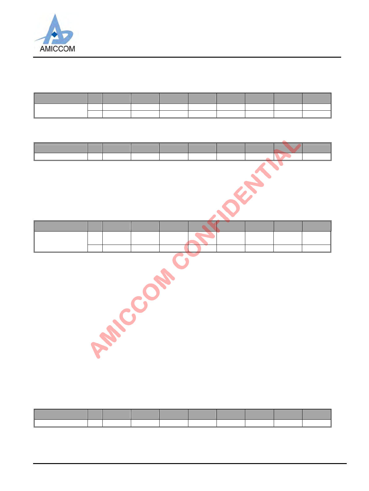
TX I WGDR GF TMDE TXDI TME FDP2 FDP1 FDP0
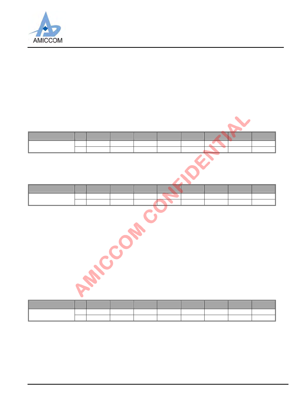
LBA7130
Oct., 2012, Version 0.6 (PRELIMINARY) 13 AMICCOM Electronics Corporation
16h
TX II WFD7 FD6 FD5 FD4 FD3 FD2 FD1 FD0
17h
Delay I WDPR2 DPR1 DPR0 TDL1 TDL0 PDL2 PDL1 PDL0
18h
Delay II WWSEL2 WSEL1 WSEL0 RSSC_D1 RSSC_D0 RS_DLY2 RS_DLY1 RS_DLY0
19h
RX WLNAGE AGCE RXSM1 RXSM0 AFCE RXDI DMG ULS
WPRS MIC IGC1 IGC0 MGC1 MGC0 LGC1 LGC0
1Ah
RX Gain I R-- MICR IGCR1 IGCR0 MGCR1 MGCR0 LGCR1 LGCR0
WRSAGC1 RSAGC0 VTL2 VTL1 VTL0 VTH2 VTH1 VTH0
1Bh
RX Gain II RRH7 RH6 RH5 RH4 RH3 RH2 RH1 RH0
W-- RDU IFS1 IFS0 RSM1 RSM0 ERSSM RSS
1Ch
RX Gain III RRL7 RL6 RL5 RL4 RL3 RL2 RL1 RL0
1Dh
RX Gain IV WLIMC IFBC1 IFBC0 IFAS MHC1 MHC0 LHC1 LHC0
W RTH7 RTH6 RTH5 RTH4 RTH3 RTH2 RTH1 RTH0
1Eh
RSSI Threshold RADC7 ADC6 ADC5 ADC4 ADC3 ADC2 ADC1 ADC0
1Fh
ADC Control WAVSEL1 AVSEL0 MVSEL1 MVSEL0 RADC FSARS XADS CDM
20h
Code I WMCS WHTS FECS CRCS IDL1 IDL0 PML1 PML0
21h
Code II WMSCRC EDRL HECS ETH2 ETH1 ETH0 PMD1 PMD0
22h
Code III WCRCINV WS6 WS5 WS4 WS3 WS2 WS1 WS0
WHFR CKGS1 CKGS0 MFBS MFB3 MFB2 MFB1 MFB0
23h
IF Calibration I R-- -- -- FBCF FB3 FB2 FB1 FB0
WPWORS TRT2 TRT1 TRT0 ASMV2 ASMV1 ASMV0 AMVS24h
IF Calibration II R-- -- -- FCD4 FCD3 FCD2 FCD1 FCD0
WROSCS RSIS VCRLS MVCS VCOC3 VCOC2 VCOC1 VCOC0
25h
VCO current
Calibration R-- -- -- VCCF VCB3 VCB2 VCB1 VCB0
WDCD1 DCD0 DAGS CWS MVBS MVB2 MVB1 MVB0
26h
VCO band
Calibration I R - - - - VBCF VB2 VB1 VB0
WMDAG7 MDAG6 MDAG5 MDAG4 MDAG3 MDAG2 MDAG1 MDAG0
27h
VCO band
Calibration II RADAG7 ADAG6 ADAG5 ADAG4 ADAG3 ADAG2 ADAG1 ADAG0
WDEVS3 DEVS2 DEVS1 DEVS0 DAMR_M VMTE_M VMS_M MSEL
28h
VCO deviation
Calibration I RDEVA7 DEVA6 DEVA5 DEVA4 DEVA3 DEVA2 DEVA1 DEVA0
WMVDS MDEV6 MDEV5 MDEV4 MDEV3 MDEV2 MDEV1 MDEV0
29h
VCO deviation
Calibration II RADEV7 ADEV6 ADEV5 ADEV4 ADEV3 ADEV2 ADEV1 ADEV0
2Ah
DASP0 WQLIM RFSP INTRC
(CSXTL5) CSXTL4 CSXTL3 CSXTL2 CSXTL1 CSXTL0
DASP1 WSTS CELS RGS RGC1 RGC0 VRPL1 VRPL0 INTPRC
DASP2 WVTRB3 VTRB2 VTRB1 VTRB0 VMRB3 VMRB2 VMRB1 VMRB0
DASP3 WDCV7 DCV6 DCV5 DCV4 DCV3 DCV2 DCV1 DCV0
WVMG7 VMG6 VMG5 VMG4 VMG3 VMG2 VMG1 VMG0
DASP4
RVMG7 VMG6 VMG5 VMG4 VMG3 VMG2 VMG1 VMG0
DASP5 W-- -- PKT1 PKT0 PKS PKIS1 PKIS0 IFPK
DASP6 W -- HPLS HRS PACTL IWS CNT MXD LXD
LBA7130
Oct., 2012, Version 0.6 (PRELIMINARY) 14 AMICCOM Electronics Corporation
2Bh
VCO modulation
Delay
WDMV1 DMV0 DEVFD2 DEVFD1 DEVFD0 DEVD2 DEVD1 DEVD0
WLVR RGV1 RGV0 QDS BVT2 BVT1 BVT0 BD_E
2Ch
Battery detect R-- RGV1 RGV0 BDF BVT2 BVT1 BVT0 BD_E
2Dh
TX test WRMP1 RMP0 TXCS PAC1 PAC0 TBG2 TBG1 TBG0
2Eh
Rx DEM test I WDMT DCM1 DCM0 MLP1 MLP0 SLF2 SLF1 SLF0
2Fh
Rx DEM test II WDCH1 DCH0 DCL2 DCL1 DCL0 RAW CDTM1 CDTM0
30h
Charge Pump
Current I
WCPM3 CPM2 CPM1 CPM0 CPT3 CPT2 CPT1 CPT0
31h
Charge Pump
Current II
WCPTX3 CPTX2 CPTX1 CPTX0 CPRX3 CPRX2 CPRX1 CPRX0
32h
Crystal test WCDPM CPS CPH CPCS DBD XCC XCP1 XCP0
33h
PLL test WMDEN OLM PRIC1 PRIC0 PRRC1 PRRC0 SDPW NSDO
34h
VCO test WDEVGD2 DEVGD1 DEVGD0 TLB1 TLB0 RLB1 RLB0 VBS
35h
RF Analog test WAGT3 AGT2 AGT1 AGT0 RFT3 RFT2 RFT1 RFT0
36h
Key Data W/R KEY7 KEY6 KEY5 KEY4 KEY3 KEY2 KEY1 KEY0
37h
Channel Select WCHI3 CHI2 CHI1 CHI0 CHD3 CHD2 CHD1 CHD0
38h
ROM_P0 WMPOR EPRG MIGS MRGS MRSS MTMS MADS MBGS
ROMP1 WAPG MPA1 MPA0 FBG4 FBG3 FBG2 FBG1 FBG0
ROMP2 WPTM1 PTM0 CTR5 CTR4 CTR3 CTR2 CTR1 CTR0
ROMP3 W-- -- CRS2 CRS1 CRS0 CTS2 CTS1 CTS0
ROMP4 W-- STMP STM5 STM4 STM3 STM2 STM1 STM0
39h
Data Rate CLK WSDR7 SDR6 SDR5 SDR4 SDR3 SDR2 SDR1 SDR0
WFCL1 FCL0 ARC3 ARC2 ARC1 ARC0 EACKS EARTS
3Ah
FCR RARTEF VPOAK RCR3 RCR2 RCR1 RCR0 EACKS EARTS
3Bh
ARD WARD7 ARD6 ARD5 ARD4 ARD3 ARD2 ARD1 ARD0
WEACKF SPSS ACKFEP5 ACKFEP4 ACKFEP3 ACKFEP2 ACKFEP1 ACKFEP0
3Ch
AFEP R-- -- EARTS EARTS EARTS TXSID2 TXSID1 TXSID0
3Dh
FCB W/R F7 F6 F5 F4 F3 F2 F1 F0
3Eh
KEYC WMEDCS AFIDS ARTMS MIDS AESS -- AKFS EDCRS
3Fh
USID WRND7 RND6 RND5 RND4 RND3 RND2 RND1 RND0
Legend: -- = unimplemented
LBA7130
Oct., 2012, Version 0.6 (PRELIMINARY) 15 AMICCOM Electronics Corporation
9.2 Control register description
9.2.1 Mode Register (Address: 00h)
Name R/W Bit 7 Bit 6 Bit 5 Bit 4 Bit 3 Bit 2 Bit 1 Bit 0
RHECF FECF CRCF CER XER PLLER TRSR TRER
Mode WRESETN RESETN RESETN RESETN RESETN RESETN RESETN RESETN
RESETN: Write to this register by 0x00 to issue reset command, then it is auto clear
HECF: Head Control Flag. (HECF will be clear after issue a strobe command.)
HEC is CRC-8 result for the optional Packet Header (Please refer to chapter 16 for details)
[0]: HEC pass. [1]: HEC error.
FECF: FEC flag. (FECF will be clear after issue any strobe command.)
[0]: FEC pass. [1]: FEC error.
CRCF: CRC flag. (CRCF will be clear after issue any strobe command.)
[0]: CRC pass. [1]: CRC error.
CER: RF chip enable status.
[0]: RF chip is disabled. [1]: RF chip is enabled.
XER: Internal crystal oscillator enabled status.
[0]: Crystal oscillator is disabled. [1]: Crystal oscillator is enabled.
PLLE: PLL enabled status.
[0]: PLL is disabled. [1]: PLL is enabled.
TRER: TRX state enabled status.
[0]: TRX is disabled. [1]: TRX is enabled.
TRSR: TRX Status Register.
[0]: RX state. [1]: TX state.
Serviceable if TRER=1 (TRX is enable).
9.2.2 Mode Control Register (Address: 01h)
Name R/W Bit 7 Bit 6 Bit 5 Bit 4 Bit 3 Bit 2 Bit 1 Bit 0
RDDPC ARSSI AIF DFCD WORE FMT FMS ADCM
Mode Control I WDDPC ARSSI AIF CD WORE FMT FMS ADCM
DDPC (Direct mode data pin control): Direct mode modem data can be accessed via SDIO pin.
[0]: Disable. [1]: Enable.
ARSSI: Auto RSSI measurement while entering RX mode.
[0]: Disable. [1]: Enable.
AIF (Auto IF Offset): RF LO frequency will auto offset one IF frequency while entering RX mode.
[0]: Disable. [1]: Enable.
CD: Carrier detector (Read only).
[0]: Input power below threshold. [1]: Input power above threshold.
DFCD: Data Filter by CD : The received packet would be filtered if the input power level is below RTH (1Eh).
[0]: Disable. [1]: Enable.
WORE: WOR (Wake On RX) Function Enable.
[0]: Disable. [1]: Enable.
FMT: Reserved for internal usage only. Shall be set to [0].
FMS: Direct/FIFO mode select.
[0]: Direct mode. [1]: FIFO mode.
ADCM: ADC measurement enable (Auto clear when done).
[0]: Disable measurement or measurement finished. [1]: Enable measurement.
Refer to chapter 17 for details.
LBA7130
Oct., 2012, Version 0.6 (PRELIMINARY) 16 AMICCOM Electronics Corporation
9.2.3 Calibration Control Register (Address: 02h)
Name R/W Bit 7 Bit 6 Bit 5 Bit 4 Bit 3 Bit 2 Bit 1 Bit 0
Mode Control II R/W -- -- -- VCC VBC VDC FBC RSSC
VCC: VCO Current calibration enable (Auto clear when done).
[0]: Disable. [1]: Enable.
VBC: VCO Bank calibration enable (Auto clear when done).
[0]: Disable. [1]: Enable.
VDC: VCO Deviation calibration enable (Auto clear when done).
[0]: Disable. [1]: Enable.
FBC: IF Filter Bank calibration enable (Auto clear when done).
[0]: Disable. [1]: Enable.
RSSC: RSSI calibration enable (Auto clear when done).
[0]: Disable. [1]: Enable.
9.2.4 FIFO Register I (Address: 03h)
Name R/W Bit 15 Bit 14 Bit 13 Bit 12 Bit 11 Bit 10 Bit 9 Bit 8
W-- -- -- -- FEP11 FEP10 FEP9 FEP8
R-- -- -- -- LENF11 LENF10 LENF9 LENF8
WFEP7 FEP6 FEP5 FEP4 FEP3 FEP2 FEP1 FEP0
FIFO I
RLENF7 LENF6 LENF5 LENF4 LENF3 LENF2 LENF1 LENF0
FEP [11:0]: FIFO End Pointer for TX FIFO and Rx FIFO.
Data Sequence is FEP[7:0] and FEP[15:8].
Please refer to chapter 16 for details.
LENF [11:0]: Received FIFO Length for dynamic FIFO function. (Ready Only)
When EDRL =1, that means dynamic FIFO is enabled, MCU can read LENF [11:0] to know the RX FIFO length of the coming
packet. Please refer to chapter 16 for details.
9.2.5 FIFO Register II (Address: 04h)
Name R/W Bit 7 Bit 6 Bit 5 Bit 4 Bit 3 Bit 2 Bit 1 Bit 0
FIFO II W FPM1 FPM0 PSA5 PSA4 PSA3 PSA2 PSA1 PSA0
FPM [1:0]: FIFO Pointer Margin
PSA [5:0]: Used for Segment FIFO.
Refer to chapter 16 for details.
9.2.6 FIFO DATA Register (Address: 05h)
Bit R/W Bit 7 Bit 6 Bit 5 Bit 4 Bit 3 Bit 2 Bit 1 Bit 0
WTX-FIFO[7:0]
Name
R/W RX-FIFO[7:0]
FIFO [7:0]: TX FIFO / RX FIFO
TX FIFO and RX FIFO share the same address (05h).
TX FIFO and RX FIFO are separated physical 64 Bytes.
Refer to chapter 16 for details.
9.2.7 ID DATA Register (Address: 06h)
Name R/W Bit 7 Bit 6 Bit 5 Bit 4 Bit 3 Bit 2 Bit 1 Bit 0
ID DATA R/W ID7 ID6 ID5 ID4 ID3 ID2 ID1 ID0
ID [7:0]: ID data.
When this address is accessed, ID Data is input or output sequential (ID Byte 0,1, 2 and 3) corresponding to Write or Read.
LBA7130
Oct., 2012, Version 0.6 (PRELIMINARY) 17 AMICCOM Electronics Corporation
Recommend to set ID Byte 0 = 5xh or Axh.
Refer to section 10.6 for details.
9.2.8 RC OSC Register I (Address: 07h)
Name R/W Bit 7 Bit 6 Bit 5 Bit 4 Bit 3 Bit 2 Bit 1 Bit 0
RRCOC7 RCOC6 RCOC5 RCOC4 RCOC3 RCOC2 RCOC1 RCOC0
RC OSC I WWOR_SL7 WOR_SL6 WOR_SL5 WOR_SL4 WOR_SL3 WOR_SL2 WOR_SL1 WOR_SL0
RCOC [7:0]: Reserved for internal usage (read only).
9.2.9 RC OSC Register II (Address: 08h)
Name R/W Bit 7 Bit 6 Bit 5 Bit 4 Bit 3 Bit 2 Bit 1 Bit 0
RC OSC II W WOR_SL9 WOR_SL8 WOR_AC5 WOR_AC4 WOR_AC3 WOR_AC2 WOR_AC1 WOR_AC0
WOR_AC [5:0]: 6-bits WOR Active Timer for WOR and TWOR Function
WOR_SL [9:0]: 10-bits WOR Sleep Timer for WOR and TWOR Function.
WOR_SL [9:0] are from address (07h) and (08h),
Active period = (WOR_AC+1) x (1/4092).
Sleep period = (WOR_SL+1) x (1/32) x (1/4092).
9.2.10 RC OSC Register III (Address: 09h)
Name R/W Bit 7 Bit 6 Bit 5 Bit 4 Bit 3 Bit 2 Bit 1 Bit 0
WRTCS RCO T2 RCOT1/
RTCC1
RCOT0/
RTCC0 CALWC RCOSC_E TSEL TWORE
RC OSC III
R-- -- -- -- CALWR -- -- --
RTCS: internal Oscillator selection in sleep mode. Recommend RTCS= [0].
[0]: RC oscillator. [1]: RTC oscillator.
RCOT[2:0]: Reserved for internal used. Recommend RCOT= [000].
RCOT[1:0]: RCOSC current select for RC oscillator calibration.
[00]: 240nA [01]: 280nA [10]: 320nA [11]: 360nA
TSEL: Timer select for TWOR function.
[0]: Use WOR_AC. [1]: Use WOR_SL.
CALWC: RC Oscillator Calibration Enable.
[0]: Disable. [1]: Enable.
CALWR: RC Oscillator Calibration ending indication.
[0]: ending. [1]: Not ending.
RCOSC_E: RC-oscillator enable.
[0]: Disable. [1]: Enable.
TSEL: Timer Duty select for TWOR function.
[0]: Use WOR_AC. [1]: Use WOR_SL.
TWORE: Enable TWOR function.
[0]: WOR mode. [1]: TWOR mode.
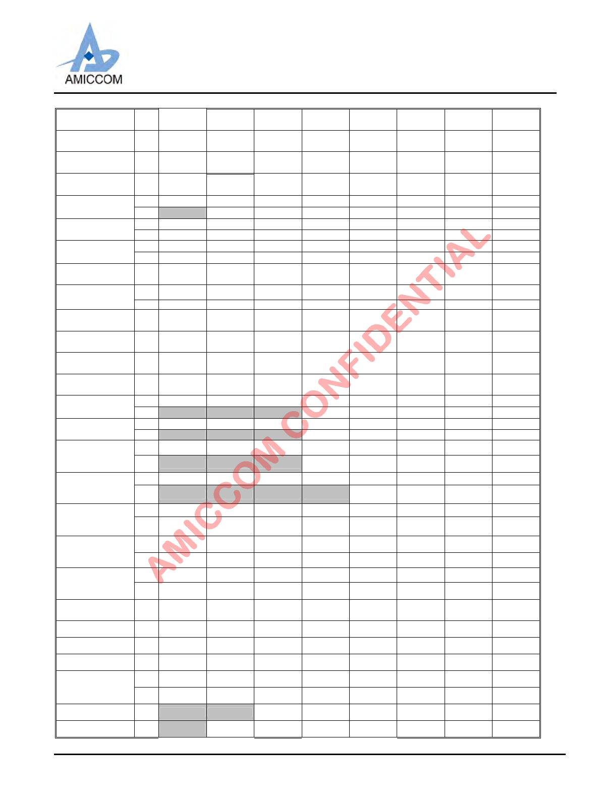
9.2.11 CKO Pin Control Register (Address: 0Ah)
Name R/W Bit 7 Bit 6 Bit 5 Bit 4 Bit 3 Bit 2 Bit 1 Bit 0
CKO Pin Control W ECKOE CKOS3 CKOS2 CKOS1 CKOS0 CKOI CKOE SCKI
ECKOE: CKO pin Output Enable.
[0]: Disable. [1]: Enable.
CKOS [3:0]: CKO pin output select.
LBA7130
Oct., 2012, Version 0.6 (PRELIMINARY) 18 AMICCOM Electronics Corporation
[0000]: DCK (TX data clock) in TX mode, RCK (RX recovery clock) in RX mode.
[0001]: DCK (TX data clock) in TX mode, RCK (RX recovery clock) in RX mode.
[0010]: FPF (FIFO pointer flag).
[0011]: EOP, EOVBC, EOFBC, EOVCC, EOVDC, RSSC_OK. (Internal usage only).
[0100]: External clock output= FSYCK / 2.
[0101]: External clock output / 2= FSYCK / 4.
[0110]: RXD
[0111]: FSYNC.
[1000]: WCK.
[1001]: PF8M.(8Mhz, internal usage)
[1010]: ROSC.
[1011]: MXDEC(SLF[0]=1:~OKADCN, SLF[1]=0: DEC , internal usage)
[1100]: BDF (Battery Detect flag).
[1101]: FSYCK ..
[1110]: VPOAK.
[1111]: WRTC (internal usage)
CKOI: CKO pin output signal invert.
[0]: Non-inverted output. [1]: Inverted output.
CKOE: CKO pin Output Enable.
[0]: High Z. [1]: Enable.
SCKI: SPI clock input invert.
[0]: Non-inverted input. [1]: Inverted input.
9.2.12 GIO1 Pin Control Register I (Address: 0Bh)
Name R/W Bit 7 Bit 6 Bit 5 Bit 4 Bit 3 Bit 2 Bit 1 Bit 0
GIO1 Pin Control I W VKM VPM GIO1S3 GIO1S2 GIO1S1 GIO1S0 GIO1I GI O1OE
VKM: Valid packet mode select.
[0]: by event.[1]: by pulse.
VPM: Valid Pulse width select.
[0]: 20u. [1]: 40u.
TX Mode (disable auto-resend, EAR=0).
LBA7130
Oct., 2012, Version 0.6 (PRELIMINARY) 19 AMICCOM Electronics Corporation
RX Mode (disable Auto-ack, EAK =0).
Note1, If auto-resend is enabled (EAR = 1), WTR behavior is different while it is output to GIO1 and GIO2.
Note2, If auto-ack is enabled (EAK = 1), WTR behavior is different while it is output to GIO1 and GIO2.
Note3, VPOAK’s behavior is controlled by VPM (0Bh) and VPW (0Bh).
Refer to chapter 19 for details
GIO1S [3:0]: GIO1 pin function select.
GIO1S [3:0] TX state RX state
[0000] WTR (Wait until TX or RX finished)
[0001] EOAC (end of access code) FSYNC (frame sync)
[0010] TMEO (TX modulation enable) CD (carrier detect)
[0011] Preamble Detect Output (PMDO)
[0100] If RCOSC_E =1, output TWOR.
If RCOSC_E =0, output CWTR signal. (internal usage)
[0101] In phase demodulator input(DMII)or VT[0] (internal usage)
[0110] SDO ( 4 wires SPI data out)
[0111] TRXD In/Out (Direct mode)
[1000] RXD (Direct mode)
[1001] TXD (Direct mode)
[1010] PDN_RX
[1011] External FSYNC input in RX direct mode (internal usage)
[1100] MXINC(SLF[0]=1:EOADC.SLF[1]=0:INC.) (internal usage)
[1101] FPF
[1110] VPOAK (Valid Packet or Auto ACK OK Output)
[1111] FMTDO (internal usage)
If GIO1S = [0100] and RCOSC_E = 0, CWTR is an internal signal to monitor TX/RX cycles of auto-ack and auto-resend.If
GIO1S = [1011] and direct mode is selected, the internal frame sync function will be disabled. In such case, A7130 supports
to accept an external frame sync signal from MCU to feed to GIO1 pin to determine the timing of fixing DC estimation voltage
of demodulator.
GIO1I: GIO1 pin output signal invert.
[0]: Non-inverted output. [1]: Inverted output.
GIO1OE: GIO1pin output enable.
[0]: High Z. [1]: Enable.
LBA7130
Oct., 2012, Version 0.6 (PRELIMINARY) 20 AMICCOM Electronics Corporation
9.2.13 GIO2 Pin Control Register II (Address: 0Ch)
Name R/W Bit 7 Bit 6 Bit 5 Bit 4 Bit 3 Bit 2 Bit 1 Bit 0
GIO2 Pin Control II W BBCKS1 BBCKS0 GIO2S3 GIO2S2 GIO2S1 GIO2S0 GIO2I GI O2OE
BBCKS [1:0]: Clock select for digital block. Recommend BBCKS = [00].
[00]: FSYCK.[01]: FSYCK / 2. [10]: FSYCK / 4. [11]: FSYCK / 8.
GIO2S [3:0]: GIO2 pin function select.
GIO2S TX state RX state
[0000] WTR (Wait until TX or RX finished)
[0001] EOAC (end of access code) FSYNC (frame sync)
[0010] TMEO (TX modulation enable) CD (carrier detect)
[0011] Preamble Detect Output (PMDO)
[0100] If RCOSC_E =1, output TWOR.
If RCOSC_E =0, output CWTR signal. (internal usage)
[0101] Quadrature phase demodulator input (DMIQ) (internal usage)
[0110] SDO (4 wires SPI data out)
[0111] TRXD In/Out (Direct mode)
[1000] RXD (Direct mode)
[1001] TXD (Direct mode)
[1010] PDN_TX
[1011] ROMOK(ROM Program OK) (internal usage)
[1100] BDF (Battery Detect Flag)
[1101] FPF
[1110] VPOAK (Valid Packet or Auto ACK OK Output)
[1111] DCK (internal usage)
If GIO2S = [0100] and RCOSC_E = 0, CWTR is an internal signal to monitor TX/RX cycles of auto-ack and auto-resend.
GIO2I: GIO2 pin output signal invert.
[0]: Non-inverted output. [1]: Inverted output.
GIO2OE: GIO2 pin Output Enable.
[0]: High Z. [1]: Enable.
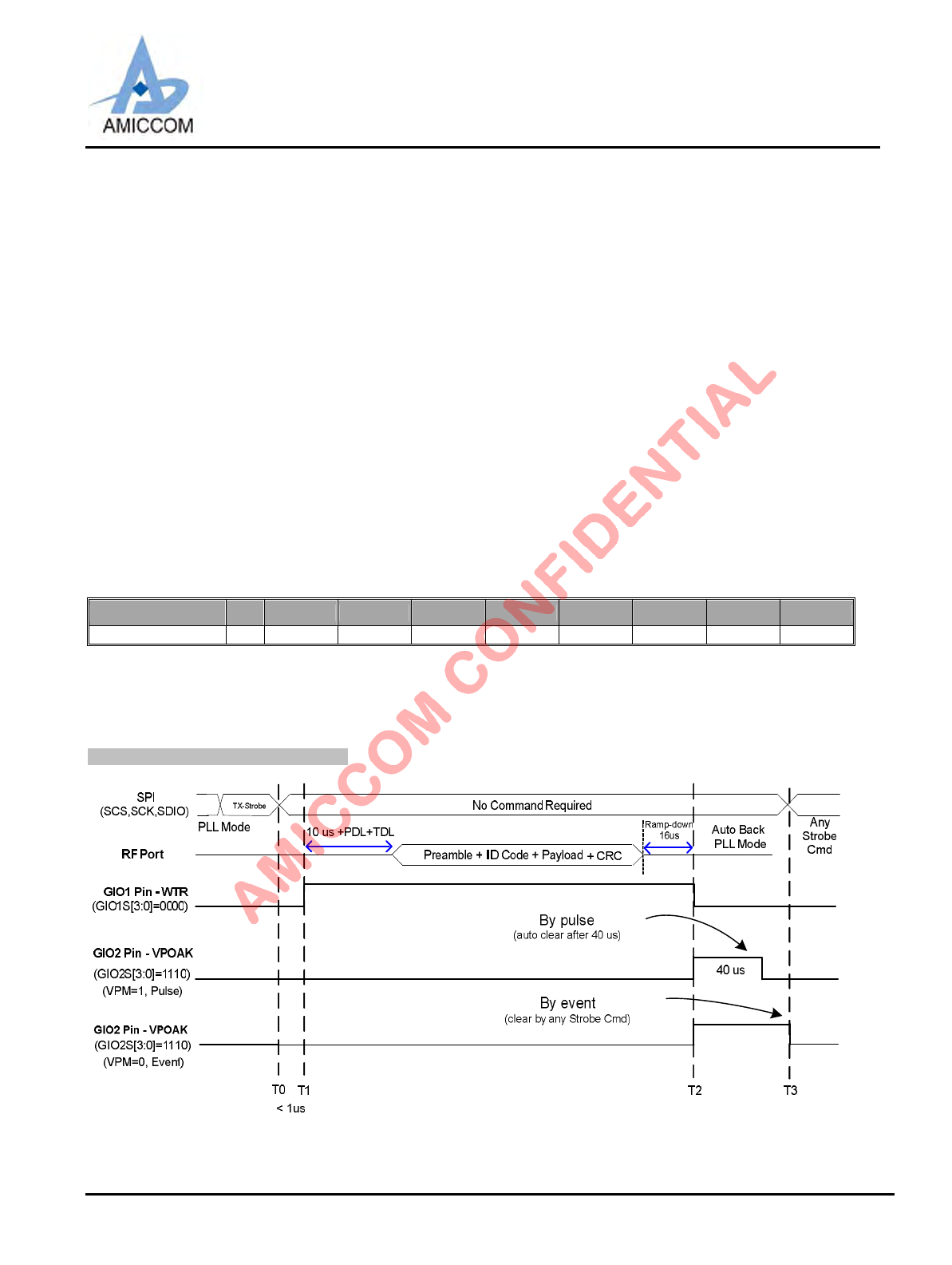
In TX mode
SPI
(SCS,SCK,SDIO)
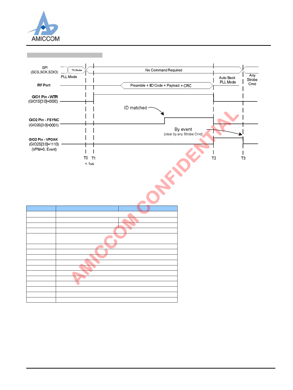
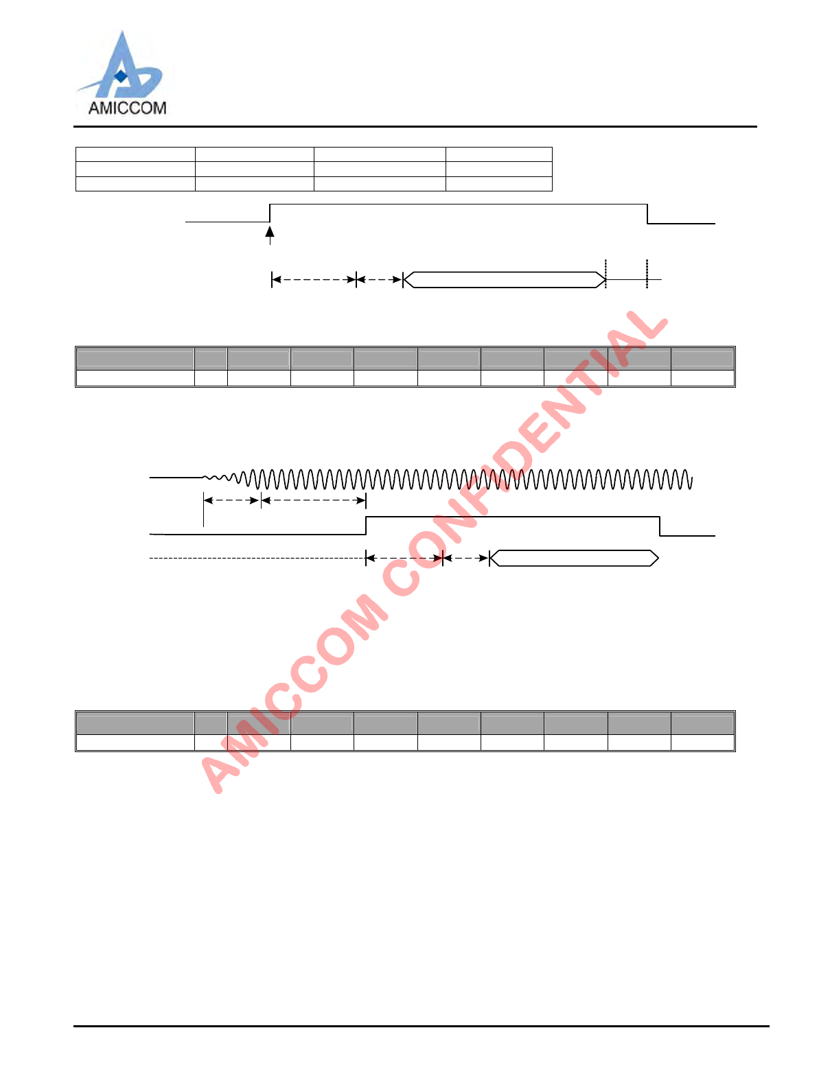
T1
No Command Required
T2
GIO1 Pin - WTR
(GIO1S[3:0]=0000)
10 us + (PDL+TDL)
Next Instruction
Preamble + ID Code + Payload
RF Port
Auto Back
PLL Mode
+ CRC
T3
PLL Mode
GIO2 Pin - TMEO
(GIO2S[3:0]=0010)
T0
16 us
PA Ramp Down
< 1us
TX-Strobe
(Output)
In RX mode
LBA7130
Oct., 2012, Version 0.6 (PRELIMINARY) 21 AMICCOM Electronics Corporation
SPI
(SCS,SCK,SDIO)
T1
No Command Required
T2
GIO1 Pin - WTR
(GIO1S[3:0]=0000)
10us+PDL+TDL
Next Instruction
Preamble + ID Code + Payload
RF Port
Auto Back
PLL Mode
+ CRC
PLL Mode
GIO2 Pin - FSYNC
(GIO2S[3:0]=0001)
T0
< 1us
RX-Strobe
(Input)
ID-Matched
9.2.14 Clock Register (Address: 0Dh)
Name R/W Bit 7 Bit 6 Bit 5 Bit 4 Bit 3 Bit 2 Bit 1 Bit 0
Clock W CGC1 CGC0 GRC3 GRC2 GRC1 GRC0 CGS XS
RIFS1 IFS0 GRC3 GRC2 GRC1 GRC0 -- --
CGC [1:0]: Clock Gen. Current select. Shall be set to [10].
GRC [3:0]: Clock generation reference counter. Recommend GRC = [0111] for 16MHz Xtal.
GRC [3:0] is used to let below formula be true when CGS = 1.
FXTAL x (DBL+1) / (GRC+1) = 2MHz.
CGS: Clock generator enable. Recommend CGS = [1]
[0]: Disable. [1]: Enable.
XS: Crystal oscillator select. Recommend XS = [1]
[0]: External clock. [1]: Crystal.
IFS [1:0]: IF band selection. (Ready only)
9.2.15 PLL Register I (Address: 0Eh)
Name R/W Bit 7 Bit 6 Bit 5 Bit 4 Bit 3 Bit 2 Bit 1 Bit 0
PLL I R/W CHN7 CHN6 CHN5 CHN4 CHN3 CHN2 CHN1 CHN0
CHN [7:0]: LO channel number select.
Refer to chapter 14 for details.
9.2.16 PLL Register II (Address: 0Fh)
Name R/W Bit 7 Bit 6 Bit 5 Bit 4 Bit 3 Bit 2 Bit 1 Bit 0
RDBL RRC1 RRC0 CHR3 CHR2 CHR1 CHR0 IP8
PLL II WDBL RRC1 RRC0 CHR3 CHR2 CHR1 CHR0 BIP8
DBL: Crystal frequency doublers selection.
[0]: Disable. FXREF = FXTAL.
[1]: Enable. FXREF =2 * FXTAL.
In FIFO mode, recommend to set DBL =0.
In Direct mode, recommend to set DBL =1.
Please refer to A7130 reference code for details.
RRC [1:0]: RF PLL reference counter setting. Recommend RRC = [00].
The PLL com parison frequency, FPFD = FCRYSTAL *(DBL+1) / (RRC+1).
LBA7130
Oct., 2012, Version 0.6 (PRELIMINARY) 22 AMICCOM Electronics Corporation
CHR [3:0]: PLL channel step setting.
In FIFO mode, recommend to set CHR [3:0] = [0111].
In Direct mode, recommend to set CHR [3:0] = [1111].
Please refer to chapter 14 and A7130 reference code for details.
9.2.17 PLL Register III (Address: 10h)
Name R/W Bit 7 Bit 6 Bit 5 Bit 4 Bit 3 Bit 2 Bit 1 Bit 0
RIP7 IP6 IP5 IP4 IP3 IP2 IP1 IP0
PLL III WBIP7 BIP6 BIP5 BIP4 BIP3 BIP2 BIP1 BIP0
BIP [8:0]: LO base frequency integer part setting. (0Fh and 10h)
In FIFO mode, recommend to set BIP [8:0] = [0x096].
In Direct mode, recommend to set BIP [8:0] = [0x04B].
Please refer to chapter 14 and A7130 reference code for details.
IP [8:0]: LO frequency integer part value.
IP [8:0] are from address (0Fh) and (10h),
Refer to chapter 14 for details.
9.2.18 PLL Register IV (Address: 11h)
Name R/W Bit 7 Bit 6 Bit 5 Bit 4 Bit 3 Bit 2 Bit 1 Bit 0
RRAC15 RAC14 RAC13 RAC12 RAC11 RAC10 RAC9 RAC8
PLL IV WBFP15 BF P14 BFP13 BFP12 BF P11 BFP10 BFP9 BFP8
9.2.19 PLL Register V (Address: 12h)
Name R/W Bit 7 Bit 6 Bit 5 Bit 4 Bit 3 Bit 2 Bit 1 Bit 0
RRAC7 RAC6 RAC5 RAC4 RAC3 RAC2 RAC1 RAC0
PLL V WBFP7 BFP6 BFP5 BFP4 BFP3 BFP2 BFP1 BFP0
BFP [15:0]: LO base frequency fractional part setting. (11h and 12h)
In FIFO mode, recommend to set BFP [15:0] = [0x0004].
In Direct mode, recommend to set BFP [15:0] = [0x0002].
Please refer to chapter 14 and A7130 reference code for details.
RAC [15:0]: Auto Frequency compensation value if AFC (19h) =1.
RAC [15:0] Note
AFC = 1 PLLFF [15:0] LO Freq. compensation value
AFC = 0 {SYNCF, AC [14:0]}
9.2.20 Channel Group Register I (Address: 13h)
Name R/W Bit 7 Bit 6 Bit 5 Bit 4 Bit 3 Bit 2 Bit 1 Bit 0
CHGI R/W CHGL7 CHGL6 CHGL5 CHGL4 CHGL3 CHGL2 CHGL1 CHGL0
CHGL [7:0]: PLL channel group low boundary setting for auto-calibration. Recommed CHGL[7:0] = 0x3C.
Refer to A7130 reference code for details.
9.2.21 Channel Group Register II (Address: 14h)
Name R/W Bit 7 Bit 6 Bit 5 Bit 4 Bit 3 Bit 2 Bit 1 Bit 0
CHGII R/W CHGH7 CHGH6 CHGH5 CHGH4 CHGH3 CHGH2 CHGH1 CHGH0
CHGH [7:0]: PLL channel group high boundary setting for auto-calibration. Recommed CHGH[7:0] = 0x78.
Refer to A7130 reference code for details.
PLL calibration frequency is divided into 3 groups by CHGL and CHGH:
Channel
Group1 0 ~ CHGL-1
Group2 CHGL ~ CHGH-1
LBA7130
Oct., 2012, Version 0.6 (PRELIMINARY) 23 AMICCOM Electronics Corporation
Group3 CHGH ~ 255
9.2.22 TX Register I (Address: 15h)
Name R/W Bit 7 Bit 6 Bit 5 Bit 4 Bit 3 Bit 2 Bit 1 Bit 0
TX I W GDR GF TMDE TXDI TME FDP2 FDP1 FDP0
GDR: Gaussian Filter Over Sampling Rate Select. Recommend GDR = [1].
[0]: BT= 0.7 [1]: BT= 0.5
GF: Gaussian Filter Select.
[0]: Disable. [1]: Enable.
TMDE: TX modulation enable for VCO modulation. Recommend TMDE = [1].
[0]: Disable. [1]: Enable.
TXDI: TX data invert. Recommend TXDI = [0].
[0]: Non-invert. [1]: Invert.
TME: TX modulation enable. Recommend TME = [1].
[0]: Disable. [1]: Enable.
FDP [2:0]: Frequency deviation power setting. Recommend FDP = [110].
In FIFO mode, recommend to set FDP [2:0] = [111].
In Direct mode, recommend to set FDP [2:0] = [110].
Please refer to chapter 14 and A7130 reference code for details.
9.2.23 TX Register II (Address: 16h)
Name R/W Bit 7 Bit 6 Bit 5 Bit 4 Bit 3 Bit 2 Bit 1 Bit 0
TXI WFD7 FD6 FD5 FD4 FD3 FD2 FD1 FD0
FD [7:0]: Frequency deviation setting.
FDEV = (FPFD /216) x FD[7:0] x 2(FDP-1).
Where FPFD= FXTAL * (DBL+1) / (RRC [1:0]+1), PLL comparison frequency.
Data Rate FDP[2:0] FD[7:0] Fdev
4Mbps FIFO mode 111 0x40 1MHz
4Mbps Direct mode 110 0x40 1MHz
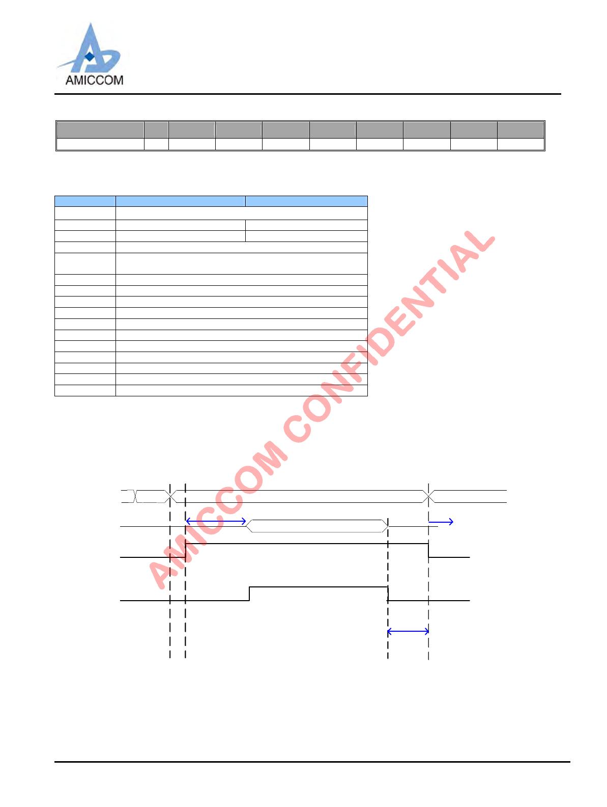
9.2.24 Delay Register I (Address: 17h)
Name R/W Bit 7 Bit 6 Bit 5 Bit 4 Bit 3 Bit 2 Bit 1 Bit 0
Delay W DPR2 DPR1 DPR0 TDL1 TDL0 PDL2 PDL1 PDL0
DPR [2:0]: Delay scale. Recommend DPR = [000].
TDL [1:0]: Delay for TX settling from WPLL to TX.
TDL Delay= 20 * (TDL [1:0]+1)*(DPR [2:0]+1) us.
DPR [2:0] TDL [1:0] WPLL to TX Note
000 00 20 us
000 01 40 us
000 10 60 us Recommend
000 11 80 us
PDL [2:0]: Delay for TX settling from PLL to WPLL.
PDL Delay= 10 + {20 * (PDL [2:0]+1)*(DPR [2:0]+1)} us.
DPR [2:0] PDL [2:0] PLL to WPLL
(LO freq changed)
Note
000 000 30 us Recommend
000 001 50 us
LBA7130
Oct., 2012, Version 0.6 (PRELIMINARY) 24 AMICCOM Electronics Corporation
000 010 70 us
000 011 90 us
000 100 110 us
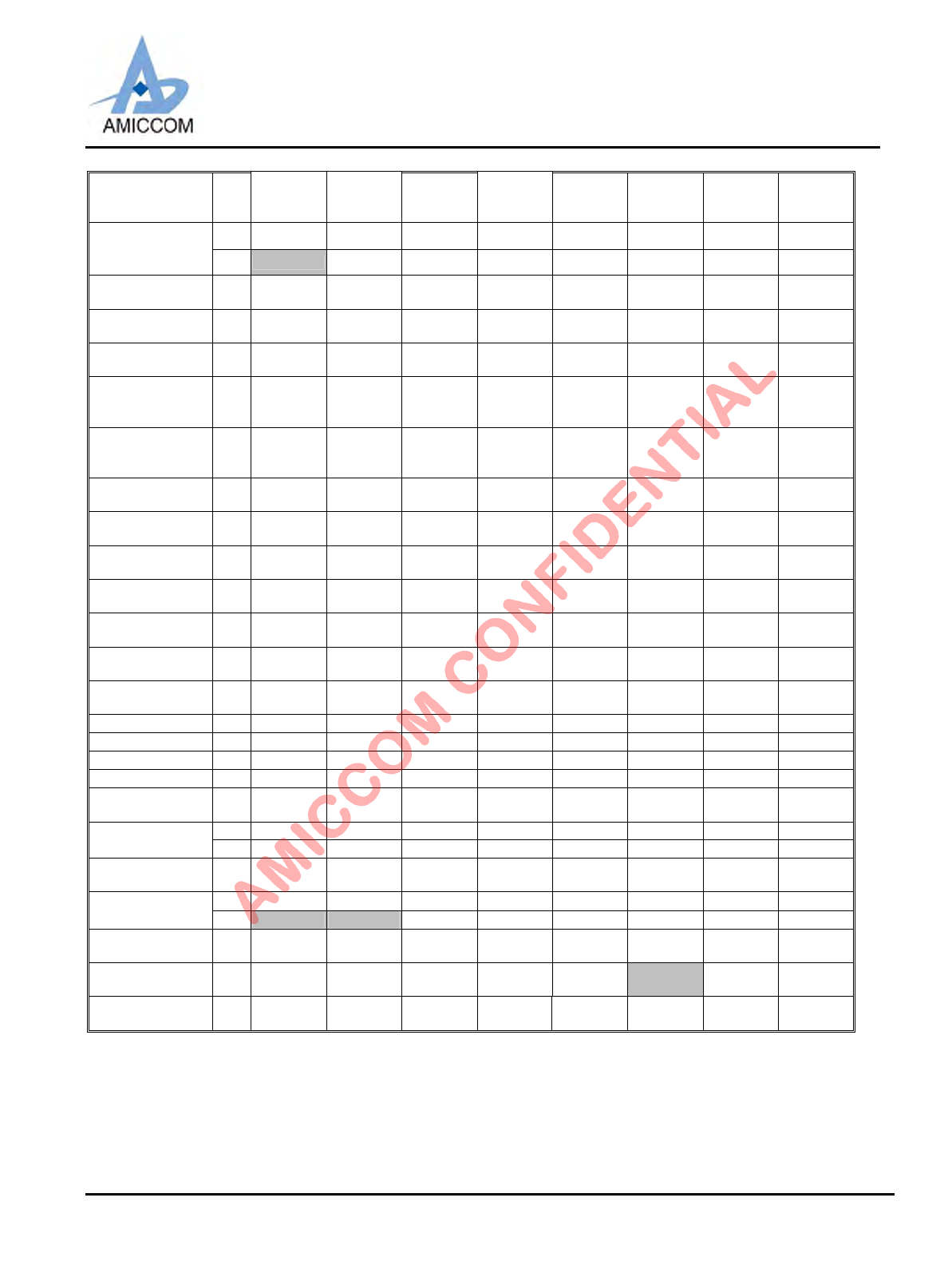
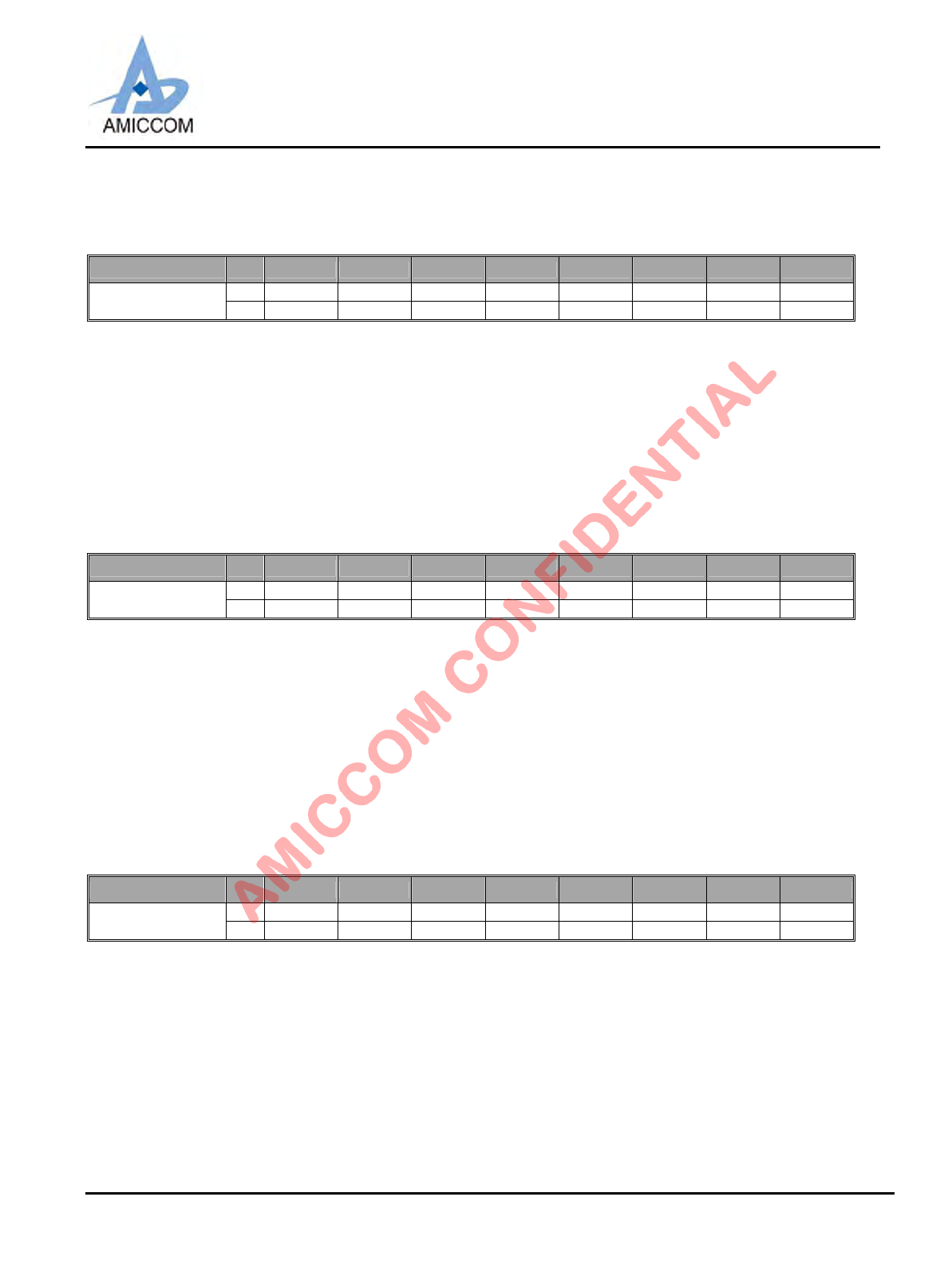
G IO 1 Pin
(WTR)
R FO Pin
TX Strobe
10 us + PD L TDL
Packet
TX Mode
PLL Mode
PA
Ramp Down
16 us
9.2.25 Delay Register II (Address: 18h)
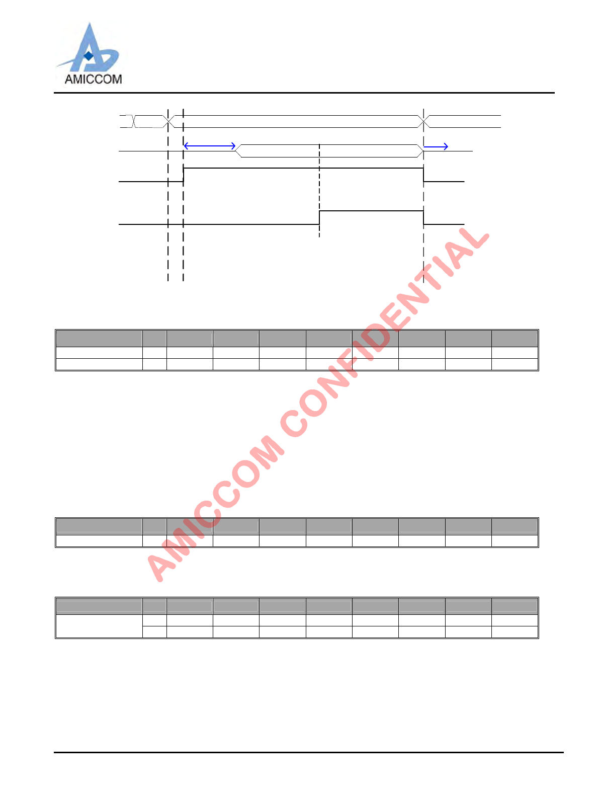
Name R/W Bit 7 Bit 6 Bit 5 Bit 4 Bit 3 Bit 2 Bit 1 Bit 0
Delay W WSEL2 WSEL1 WSEL0 RSSC_D1 RSSC_D0 RS_DLY2 RS_DLY1 RS_DLY0
WSEL [2:0]: XTAL settling delay setting (200us ~ 2.5ms). Recommend WSEL = [011].
[000]: 200us. [001]: 400us. [010]: 600us. [011]: 800us.
[100]: 1ms. [101]: 1.5ms. [110]: 2ms. [111]: 2.5ms.
GIO1 Pin
(WTR)
Crystal
O scilla tor
10 us + PDL TDL
300 us WSEL
Id le
mode
TX or RX Strobe Cm d
Packet (Preamble + ID + Payload)
R FO Pin
RSSC_D [1:0]: RSSI calibration switching time (10us ~ 40us). Recommend RSSC_D = [00].
[00]: 10us. [01]: 20us. [10]: 30us. [11]: 40us.
RS_DLY [2:0]: RSSI measurement delay (10us ~ 80us). Recommend RS_DLY = [000].
[000]: 10us. [001]: 20us. [010]: 30us. [011]: 40us.
[100]: 50us. [101]: 60us. [110]: 70us. [111]: 80us.
9.2.26 RX Register (Address: 19h)
Name R/W Bit 7 Bit 6 Bit 5 Bit 4 Bit 3 Bit 2 Bit 1 Bit 0
RX W LNAGE AGCE RXSM1 RXSM0 AFCE RXDI DMG ULS
LNAGE: Auto LNA Gain Control Select.
[0]: Disable. [1]: Enable.
AGCE: Auto Front end Gain Control Select.
[0]: Disable. [1]: Enable.
RXSM1: RX clock recovery circuit moving average filter length. Recommend RXSM1 = [1].
[0]: 4 bits. [1]: 8 bits.
RXSM0: Demodulator LPF Bandwidth Select. Recommend RXSM0 = [1].
[0]: 2*IF. [1]: 1*IF.
AFCE: Frequency compensation select.
[0]: Disable. [ 1]: Enable.
RXDI: RX data output invert. Recommend RXDI = [0].
[0]: Non-inverted output. [1]: Inverted output.
DMG: Demodulator Gain Select. Recommend DMG = [1].
[0]: x 1. [1]: x 3.
LBA7130
Oct., 2012, Version 0.6 (PRELIMINARY) 25 AMICCOM Electronics Corporation
ULS: RX Up/Low side band select. Recommend ULS = [0].
[0]: Up side band, [1]: Low side band.
Refer to section 14.2 for details.
9.2.27 RX Gain Register I (Address: 1Ah)
Name R/W Bit 7 Bit 6 Bit 5 Bit 4 Bit 3 Bit 2 Bit 1 Bit 0
WPRS MIC IGC1 IGC0 MGC1 MGC0 LGC1 LGC0
RX Gain I R-- MICR IGCR1 IGCR0 MGCR1 MGCR0 LGCR1 LGCR0
PRS: Limiter amplifier discharge manual select. Recommend PRS =[0].
MIC: Mixer buffer gain setting. Recommend MIC =[1].
[0]: 0dB. [1]: 6dB.
IGC [1:0]: IFA Attenuation Select. Recommend IGC =[10].
[00]: 0dB. [01]: 6dB. [10]: 12dB. [11]: 18dB.
MGC [1:0]: Mixer Gain Attenuation select. Recommend MGC =[11].
[00]: 0dB. [01]: 6dB. [10]: 12dB. [11]: 18dB.
LGC [1:0]: LNA Gain Attenuation select. Recommend LGC =[11].
[00]: 0dB. [01]: 6dB. [10]: 12dB. [11]: 18dB.
9.2.28 RX Gain Register II (Address: 1Bh)
Name R/W Bit 7 Bit 6 Bit 5 Bit 4 Bit 3 Bit 2 Bit 1 Bit 0
RRH7 RH6 RH5 RH4 RH3 RH2 RH1 RH0
RX Gain II WRSAGC1 RSAGC0 VTL2 VTL1 VTL0 VTH2 VTH1 VTH0
RSAGC [1:0]: AGC clock select. Recommend RSAGC = [11].
[00]: IF / 8. [01]: IF / 4. [10]: IF/ 2. [11]: IF.
VTL [2:0]: VCO tuning voltage lower threshold level setting. Recommend VTL = [000].
[000]: 0.1V. [001]: 0.2V. [010]: 0.3V. [011]: 0.4V.
[100]: 0.5V. [101]: 0.6V. [110]: 0.7V. [111]: 0.8V
VTH [2:0]: VCO tuning voltage upper threshold level setting. Recommend VTH = [010].
[000]: VDD_A – 0.6V. [001]: VDD_A – 0.7V. [010]: VDD_A – 0.8V. [011]: VDD_A – 0.9V
[100]: VDD_A – 1.0V. [101]: VDD_A – 1.1V. [110]: VDD_A – 1.2V. [111]: VDD_A – 1.3V
Remark: VDD_A is on chip analog regulator output voltage where is set to 1.8V.
RH [7:0]: RSSI Calibration High Threshold. (Read only)
9.2.29 RX Gain Register III (Address: 1Ch)
Name R/W Bit 7 Bit 6 Bit 5 Bit 4 Bit 3 Bit 2 Bit 1 Bit 0
RRL7 RL6 RL5 RL4 RL3 RL2 RL1 RL0
RX Gain III W-- RDU IFS1 IFS0 RSM1 RSM0 ERSSM RSS
RDU: Clock Generator Select. Recommend RDU = [0].
[0]: 128MHZ [1]: 96MHZ.
IFS [1:0]: IF Frequency Select.
[00]: reserved. [01]: reserved. [10]: reserved [11]: 4MHZ.
RSM [1:0]: RSSI Margin = RTH – RTL. Recommend RSM = [11].
[00]: 5. [01]: 10. [10]: 15. [11]: 20.
Refer to chapter 17 for details.
ERSSM: Ending Mode Select in RSSI Measurement. Recommend ERSSM = [0].
[0]: RSSI ending by RX. [1]: RSSI ending by SYNC_Ok.
RSS: RSSI measurement select. (XADS=0, RSS=0, default mode is thermal sensor.)
[0]: Disable. [1]: Enable (recommend).
LBA7130
Oct., 2012, Version 0.6 (PRELIMINARY) 26 AMICCOM Electronics Corporation
RL [7:0]: RSSI Calibration Low Threshold. (Ready only)
9.2.30 RX Gain Register IV (Address: 1Dh)
Name R/W Bit 7 Bit 6 Bit 5 Bit 4 Bit 3 Bit 2 Bit 1 Bit 0
RX Gain III W LIMC IFBC1 IFBC0 IFAS MHC1 MHC0 LHC1 LHC0
LIMC: IF limiter current select. Recommend LIMC = [1].
[0]: 0.3mA. [1]: 0.6mA.
IFBC [1:0]: IF BPF current Select. Recommend IFBC = [11].
[00]: 0.75 mA.. [01]: 1.4mA. [10]: 2.1mA. [11]: 3.5mA.
IFAS: IF Amp current select. Recommend IFAS = [0].
[0]: 0.3mA. [1]: 0.6mA.
MHC: Mixer Current Select. Recommend MHC = [01].
[00]: 0.6mA. [01]: 1.2mA. [10]: reserved. [11]: reserved.
LHC[1:0]: LNA Current Select. Recommend LHC = [11].
[00]: 0.5mA. [01]: 1mA. [10]: 1.5mA. [11]: 2mA.
9.2.31 RSSI Threshold Register (Address: 1Eh)
Name R/W Bit 7 Bit 6 Bit 5 Bit 4 Bit 3 Bit 2 Bit 1 Bit 0
RADC7 ADC6 ADC5 ADC4 ADC3 ADC2 ADC1 ADC0
RSSI Threshold WRTH7 RTH6 RTH5 RTH4 RTH3 RTH2 RTH1 RTH0
RTH [7:0]: Carrier detect threshold.
Refer to Chapter 17 for details.
CD (Carrier Detect)=1 when RSSI ≧ RT H.
CD (Carrier Detect)=0 when RSSI < RTL.
ADC [7:0]: ADC output value for RSSI measurement.
ADC input voltage= 1.2 * ADC [7:0] / 256 V.
9.2.32 ADC Control Register (Address: 1Fh)
Name R/W Bit 7 Bit 6 Bit 5 Bit 4 Bit 3 Bit 2 Bit 1 Bit 0
ADC Control W AVSEL1 AVSEL0 MVSEL1 MVSEL0 RADC FSARS XADS CDM
AVSEL [1:0]: ADC average times (for Carrier / temeperature sensor / external ADC). Recommend AVSEL = [11].
[00]: No average. [01]: Average 2 times. [10]: Average 4 times. [11]: Average 8 times.
MVSEL [1:0]: ADC average times (for VCO calibration and RSSI ). Recommend MVSEL = [11].
[00]: Average 8 times. [01]: Average 16 times. [10]: Average 32 times. [11]: Average 64 times.
RADC: ADC Read Out Average Mode. Recommend RADC = [0].
[0]: by AVSEL.
[1]: by MVSEL.
FSARS: ADC clock select. Recommend FSARS = [0].
[0]: 4MHz. [1]: 8MHz.
XADS: External ADC Input Signal Select.
[0]: Disable. [1]: Enable.
CDM: RSSI measurement mode. Recommend CDM = [1].
[0]: Single mode. [1]: Continuous mode.
9.2.33 Code Register I (Address: 20h)
Name R/W Bit 7 Bit 6 Bit 5 Bit 4 Bit 3 Bit 2 Bit 1 Bit 0
Code I W MCS WHTS FECS CRCS IDL1 IDL0 PML1 PML0
LBA7130
Oct., 2012, Version 0.6 (PRELIMINARY) 27 AMICCOM Electronics Corporation
MSC: Manchester Enable.
[0]: Disable. [1]: Enable.
WHTS: Data Whitening (Data Encryption) Select.
[0]: Disable. [1]: Enable (The data is whitening by multiplying PN7).
FECS: FEC Select.
[0]: Disable. [1]: Enable (The FEC is (7, 4) Hamming code).
CRCS: CRC Select. Recommend CRCS = [1].
[0]: Disable. [1]: Enable.
IDL [1:0]: ID Code Length Select. Recommend IDL= [01].
[00]: 2 bytes. [01]: 4 bytes. [10]: 6 bytes. [11]: 8 bytes.
PML [1:0]: Preamble Length Select. Recommend PML= [11].
[00]: 1 byte. [01]: 2 bytes. [10]: 3 bytes. [11]: 4 bytes.
9.2.34 Code Register II (Address: 21h)
Name R/W Bit 7 Bit 6 Bit 5 Bit 4 Bit 3 Bit 2 Bit 1 Bit 0
Code II W MSCRC EDRL HECS ETH2 ETH1 ETH0 PMD1 PMD0
MSCRC: Mask CRC (CRC Data Filtering Enable). Recommend MSCRC = [1].
[0]: Disable. [1]: Enable.
EDRL: Enable FIFO Dynamic Length
[0]: Disable. [1]: Enable.
Please refer to chapter 16 for details.
HECS: HEC Header CRC-8 select.
[0]: Disable. [1]: Enable.
Please refer to chapter 16 for details.
ETH [2:0]: Received ID Code Error Tolerance. Recommend ETH = [001].
[000]: 0 bit, [001]: 1 bit. [010]: 2 bit. [011]: 3 bit. [100]: 4 bit, [101]: 5 bit. [110]: 6 bit. [111]: 7 bit.
PMD [1:0]: Preamble pattern detection length. Recommend PMD = [10].
[00]: 0bit. [01]: 4bits. [10]: 8bits. [11]: 16bits.
9.2.35 Code Register III (Address: 22h)
Name R/W Bit 7 Bit 6 Bit 5 Bit 4 Bit 3 Bit 2 Bit 1 Bit 0
Code III W CRCINV WS6 WS5 WS4 WS3 WS2 WS1 WS0
CRCINV: CRC Inverted Select.
[0]: Non-inverted. [1]: inverted.
WS [6:0]: Data Whitening seed setting (data encryption key).
The data is whitened by multiplying with PN7.
Please refer to chapter 16 for details.
9.2.36 IF Calibration Register I (Address: 23h)
Name R/W Bit 7 Bit 6 Bit 5 Bit 4 Bit 3 Bit 2 Bit 1 Bit 0
R-- -- -- FBCF FB3 FB2 FB1 FB0
IF Calibration I WHFR CKGS1 CKGS0 MFBS MFB3 MFB2 MFB1 MFB0
HFR: Half Rate setting. Recommend HFR = [0].
[0]: Clk gen. by 32 x Data Rate. [1]: Clk gen. by 16 x Data Rate.
CKGS[1:0]: Clock gen. data rate manual setting. Recommend CKGS = [11].
[00]: reserved.[01]: reserved. [10]: reserved.[11]: 4MHZ.
When RDU=0, CKGS[1:0] = IFS[1:0]
When RDU=1, CKGS[1:0] = Manual setting.
MFBS: IF filter calibration value select. Recommend MFBS = [0].
LBA7130
Oct., 2012, Version 0.6 (PRELIMINARY) 28 AMICCOM Electronics Corporation
[0]: Auto calibration value. [1]: Manual calibration value.
MFB [3:0]: IF filter manual calibration value.
FBCF: IF filter auto calibration flag (read only).
[0]: Pass. [1]: Fail.
FB [3:0]: IF filter calibration value (read only).
MFBS= 0: Auto calibration value (AFB),
MFBS= 1: Manual calibration value (MFB).
9.2.37 IF Calibration Register II (Address: 24h)
Name R/W Bit 7 Bit 6 Bit 5 Bit 4 Bit 3 Bit 2 Bit 1 Bit 0
R-- -- FCD4 FCD3 FCD2 FCD1 FCD0
IF Calibration II WPWORS TRT2 TRT1 TRT0 ASMV2 ASMV1 ASMV0 AMVS
PWORS: TX high power setting. Recommend PWORS = [1].
[0]: Disable. [1]: Enable.
TRT [2:0]: TX Ramp down discharge current select. Recommend TRT = [111].
AMSV [2:0]: TX Ramp up Timing Select. Recommend AMSV = [111].
[000]: 2us, [001]: 4us. [010]: 6us. [011]: 8us. [100]: 10us, [101]: 12us. [110]: 14us. [111]: 16us.
Real case of TX ramping up is AMSV [2:0] multiplied by 2^(RMP[1:0])
AMVS: TX Ramp Up Enable. Recommend AMVS = [1].
[0]: Disable. [1]: Enable.
FCD [4:0]: IF filter calibration deviation from goal (read only).
9.2.38 VCO current Calibration Register (Address: 25h)
Name R/W Bit 7 Bit 6 Bit 5 Bit 4 Bit 3 Bit 2 Bit 1 Bit 0
R-- -- -- VCCF VCB3 VCB2 VCB1 VCB0
VCO current
Calibration WROSCS RSIS VCRLS MVCS VCO C3 VCOC2 VCOC1 VCOC0
ROSCS: WOR RC select. Recommend ROSCS = [1]
RSIS: WOR current select. Recommend RSIS = [0]
VCRLS: VCO Current Resistor Select. Recommend VCRLS = [0]
[0]: low current select. [1]: high current select.
MVCS: VCO current calibration value select. Recommend MVCS = [0].
[0]: Auto calibration value. [1]: Manual calibration value.
VCOC [3:0]: VCO current manual calibration value.
VCCF: VCO Current Auto Calibration Flag (read only).
[0]: Pass. [1]: Fail.
VCB [3:0]: VCO current calibration value (read only).
MVCS= 0: Auto calibration value (VCB).
MVCS= 1: Manual calibration value (VCOC).
9.2.39 VCO band Calibration Register I (Address: 26h)
Name R/W Bit 7 Bit 6 Bit 5 Bit 4 Bit 3 Bit 2 Bit 1 Bit 0
R-- -- -- -- VBCF VB2 VB1 VB0
VCO Single band
Calibration I WDCD1 DCD0 DAGS CWS MVBS MVB2 MVB1 MVB0
DCD [1:0]: VCO Deviation Calibration Delay. Recommend DCD = [11].
Delay time = PDL (Delay Register I, 17h) × ( DDC + 1 ).
DAGS: DAG Calibration Value Select. Recommend DAGS = [0].
[0]: Auto calibration value. [1]: Manual calibration value.
LBA7130
Oct., 2012, Version 0.6 (PRELIMINARY) 29 AMICCOM Electronics Corporation
CWS: Clock Disable for VCO Modulation. Recommend CWS = [1].
[0]: Enable. [1]: Disable.
MVBS: VCO bank calibration value select. Recommend MVBS = [0].
[0]: Auto calibration value. [1]: Manual calibration value.
MVB [2:0]: VCO band manual calibration value.
VBCF: VCO band auto calibration flag (read only).
[0]: Pass. [1]: Fail.
VB [2:0]: VCO bank calibration value (read only).
MVBS= 0: Auto calibration value (AVB).
MVBS= 1: Manual calibration value (MVB).
9.2.40 VCO band Calibration Register II (Address: 27h)
Name R/W Bit 7 Bit 6 Bit 5 Bit 4 Bit 3 Bit 2 Bit 1 Bit 0
WDAGM7 DAGM6 DAGM5 DAGM4 DAGM3 DAGM2 DAGM1 DAGM0
VCO Single band
Calibration II RDAGB7 DAGB6 DAGB5 DAGB4 DAGB3 DAGB2 DAGB1 DAGB0
DAGM [7:0]: DAG Manual Setting Value.
DAGB [7:0]: Auto DAG Calibration Value (read only).
9.2.41 VCO Deviation Calibration Register I (Address: 28h)
Name R/W Bit 7 Bit 6 Bit 5 Bit 4 Bit 3 Bit 2 Bit 1 Bit 0
RDEVA7 DEVA6 DEVA5 DEVA4 DEVA3 DEVA2 DEVA1 DEVA0
VCO Deviation
Calibration I WDEVS3 DEVS2 DEVS1 DEVS0 DAMR_M VMTE_M VMS_M MSEL
DEVS [3:0]: Deviation Output Scaling. Recommend DEVS = [0111].
DAMR_M: DAMR Manual Enable. Recommend DAMR_M = [0].
[0]: Disable. [1]: Enable.
VMTE_M: VMT Manual Enable. Recommend VMTE_M = [0].
[0]: Disable. [1]: Enable.
VMS_M: VM Manual Enable. Recommend VMS_M = [0].
[0]: Disable. [1]: Enable.
MSEL: VMS, VMTE and DAMR control select. Recommend MSEL = [0].
[0]: Auto control. [1]: Manual control.
DEVA [7:0]: Deviation Output Value (read only).
MVDS (29h)= 0: Auto calibration value ((DEVC / 8) × (DEVS + 1)),
MVDS (29h)= 1: Manual calibration value (DEVM [6:0]).
9.2.42 VCO Deviation Calibration Register II (Address: 29h)
Name R/W Bit 7 Bit 6 Bit 5 Bit 4 Bit 3 Bit 2 Bit 1 Bit 0
RDEVC7 DEVC6 DEVC5 DEVC4 DEVC3 DEVC2 DEVC1 DEVC0
VCO Deviation
Calibration II WMVDS DEVM 6 DEVM5 DEVM4 DEVM3 DEVM2 DEVM1 DEVM0
MVDS: VCO Deviation Calibration Select. Recommend MVDS = [0].
[0]: Auto calibration value. [1]: Manual calibration value.
DEVM [6:0]: VCO Deviation Manual Calibration Value.
DEVC [7:0]: VCO Deviation Auto Calibration Value (read only).
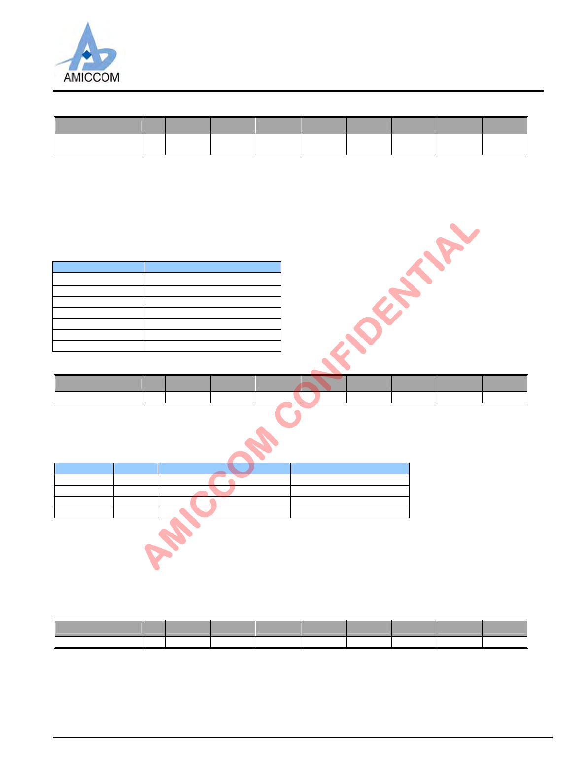
LBA7130
Oct., 2012, Version 0.6 (PRELIMINARY) 30 AMICCOM Electronics Corporation
9.2.43 DASP0 (Address: 2Ah, Page 0 by AGT [3:0]=0)
Name R/W Bit 7 Bit 6 Bit 5 Bit 4 Bit 3 Bit 2 Bit 1 Bit 0
DASP0 W QLIM RFSP INTXC
(CSXTL5) CSXTL4 CSXTL3 CSXTL2 CSXTL1 CSXTL0
QLIM: quick charge select for IF limiter amp. Recommend QLIM = [0].
[0]: disable. [1]: enable. (QLIM fall down delay 10 us).
RFSP: RF single port Select. Recommend RFSP = [0].
[0]: LNA (RFI) and PA (RFO) are combined internally to RFI pin.
[1]: LNA (RFI) and PA (RFO) are separated to RFI pin and RFO pin.
INTXC: internal crystal oscillator capacitor selection. Recommend INTXC = [1].
[0]: disable. [1]: enable.
CSXTAL[4:0]: On-chip Crystal loading select. Recommend CSXTAL = [10100] if Xtal Cload = 18 pF.
{INTXC,CSXTAL[4:0]} On-chip Xtal Capacitor (pF)
0XXXXX 0
100000 16
100001 17
100010 18
…
111110 46
111111 47
9.2.43 DASP1 (Address: 2Ah, Page 1 by AGT[3:0]=1)
Name R/W Bit 7 Bit 6 Bit 5 Bit 4 Bit 3 Bit 2 Bit 1 Bit 0
DASP1 W STS CELS RGS RGC1 RGC0 VRPL1 VRPL0 INTPRC
STS: Start up mode select. Shall be set to [0].
CELS: Digital voltage select in standby mode. Recommend CELS = [1].
RGS: Low Power Regulator Voltage Select. Recommend RGS = [0].
LVR (2Ch) RGS Low Power Regulator Voltage Note
0 0 3/5 *REGI
0 1 3/4 * REGI
1 0 1.8 V Recommended
1 1 1.6 V
RGC [1:0]: Low power band-gap current select. Recommend RGC = [01].
VRPL [1:0]: internal PLL loop filter resistor value select. Recommend VRPL = [00].
[00]: 500 ohm. [01]: 666 ohm. [10]: 1 K ohm. [11]: 2K ohm.
INTPRC: Internal PLL loop filter resistor and capacitor select. Recommend INTPRC = [1].
[0]: disable. [1]: enable
9.2.43 DASP2 (Address: 2Ah, Page 2 by AGT[3:0]=2)
Name R/W Bit 7 Bit 6 Bit 5 Bit 4 Bit 3 Bit 2 Bit 1 Bit 0
DASP2 W VTRB3 VTRB2 VTRB1 VTRB0 VMRB3 VMRB2 VMRB1 VMRB0
VTRB [3:0]: Resistor Bank for VT RC Filtering. Shall be set to [0000].
VMRB [3:0]: Resistor Bank for VM RC Filtering. Shall be set to [0000].
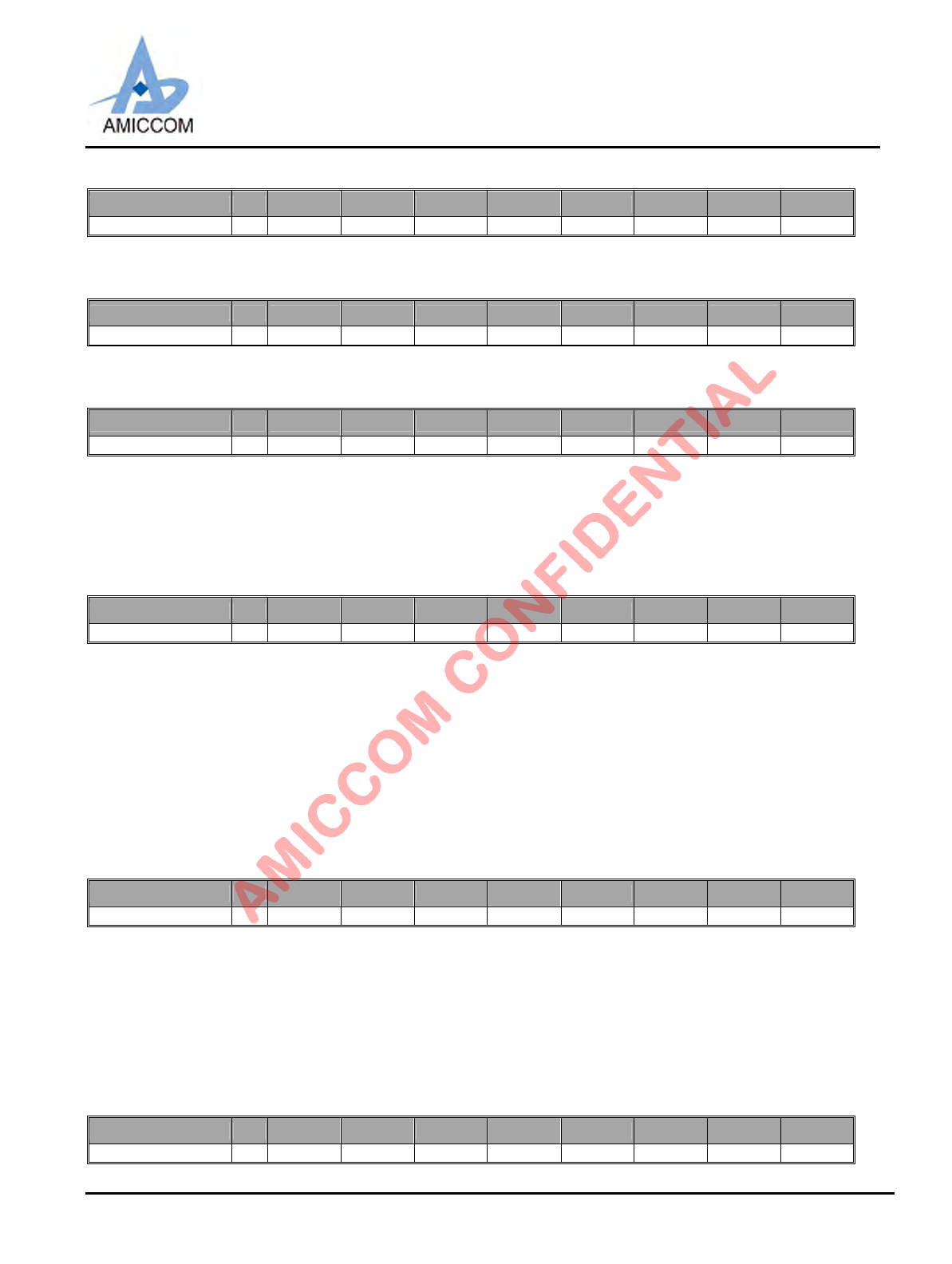
LBA7130
Oct., 2012, Version 0.6 (PRELIMINARY) 31 AMICCOM Electronics Corporation
9.2.43 DASP3 (Address: 2Ah, Page 3 by AGT[3:0]=3)
Name R/W Bit 7 Bit 6 Bit 5 Bit 4 Bit 3 Bit 2 Bit 1 Bit 0
DASP3 W DCV7 DCV6 DCV5 DCV4 DCV3 DCV2 DCV1 DCV0
DCV [7:0]: Demodulator Fix mode DC value. Recommend DCV = [0x80].
9.2.43 DASP4 (Address: 2Ah, Page 4 by AGT[3:0]=4)
Name R/W Bit 7 Bit 6 Bit 5 Bit 4 Bit 3 Bit 2 Bit 1 Bit 0
DASP4 W/R VMG7VMG6VMG5 VMG4 VMG3 VMG2 VMG1 VMG0
VMG [7:0]: VM Center Value for Deviation Calibration. Recommend VMG [7:0] = [0x80].
9.2.43 DASP5 (Address: 2Ah, Page 5 by AGT[3:0]=5)
Name R/W Bit 7 Bit 6 Bit 5 Bit 4 Bit 3 Bit 2 Bit 1 Bit 0
DASP5 W -- -- PKT1 PKT0 PKS PKIS1 PKIS0 IFPK
PKT[1:0]: VCO Peak Detect Current Select. Recommend PKT = [00].
PKS: VCO Current Calibration Mode Select. Recommend PKS = [0].
PKIS[1:0]: AGC Peak Detect Current Select. Recommend PKIS = [00].
IFPK: AGC Amplifier Current Select. Recommend IFPK = [0].
9.2.43 DASP6 (Address: 2Ah, Page 6 by AGT[3:0]=6)
Name R/W Bit 7 Bit 6 Bit 5 Bit 4 Bit 3 Bit 2 Bit 1 Bit 0
DASP6 W -- HPLS HRS PACTL IWS CNT MXD LXD
HPLS: High Power LNA Gain Select. Recommend HPLS = [0].
[0]: LGC set to 6dB when in TX Mode. [1]: LGC set to 24dB when in TX Mode.
HRS: Reserved for internal usage only. Shall be set to [0].
PACTL: Reserved for internal usage only. Shall be set to [0].
IWS: Reserved for internal usage only. Shall be set to [1].
CNT: Reserved for internal usage only. Shall be set to [0].
MXD: Reserved for internal usage only. Shall be set to [1].
LXD: Reserved for internal usage only. Shall be set to [0].
9.2.43 DASP7 (Address: 2Ah, Page 7 by AGT[3:0]=7)
Name R/W Bit 7 Bit 6 Bit 5 Bit 4 Bit 3 Bit 2 Bit 1 Bit 0
DASP7 W XDS VRSEL MS MSCL4 MSCL3 MSCL2 MSCL1 MSCL0
XDS: VCO Modulation Data Sampling Clock selection. Recommend XDS = [0].
[0]: 8x over-sampling Clock. [ 1]: XCPCK Clock.
VRSEL: AGC Function select. Recommend VRSEL = [1].
[0]: RSSI AGC. [1 ]: Normal AGC.
MS: AGC Manual scale select. Recommend MS = [0].
[0]: By (RH−RL). [ 1]: By MSCL[4:0].
MSCL[4:0]: AGC Manual Scale setting. Recommend MSCL = [00000].
9.2.44 VCO Modulation Delay Register (Address: 2Bh)
Bit R/W Bit 7 Bit 6 Bit 5 Bit 4 Bit 3 Bit 2 Bit 1 Bit 0
Name WDMV1 DMV0 DEVFD2 DEVFD1 DEVFD0 DEVD2 DEVD1 DEVD0
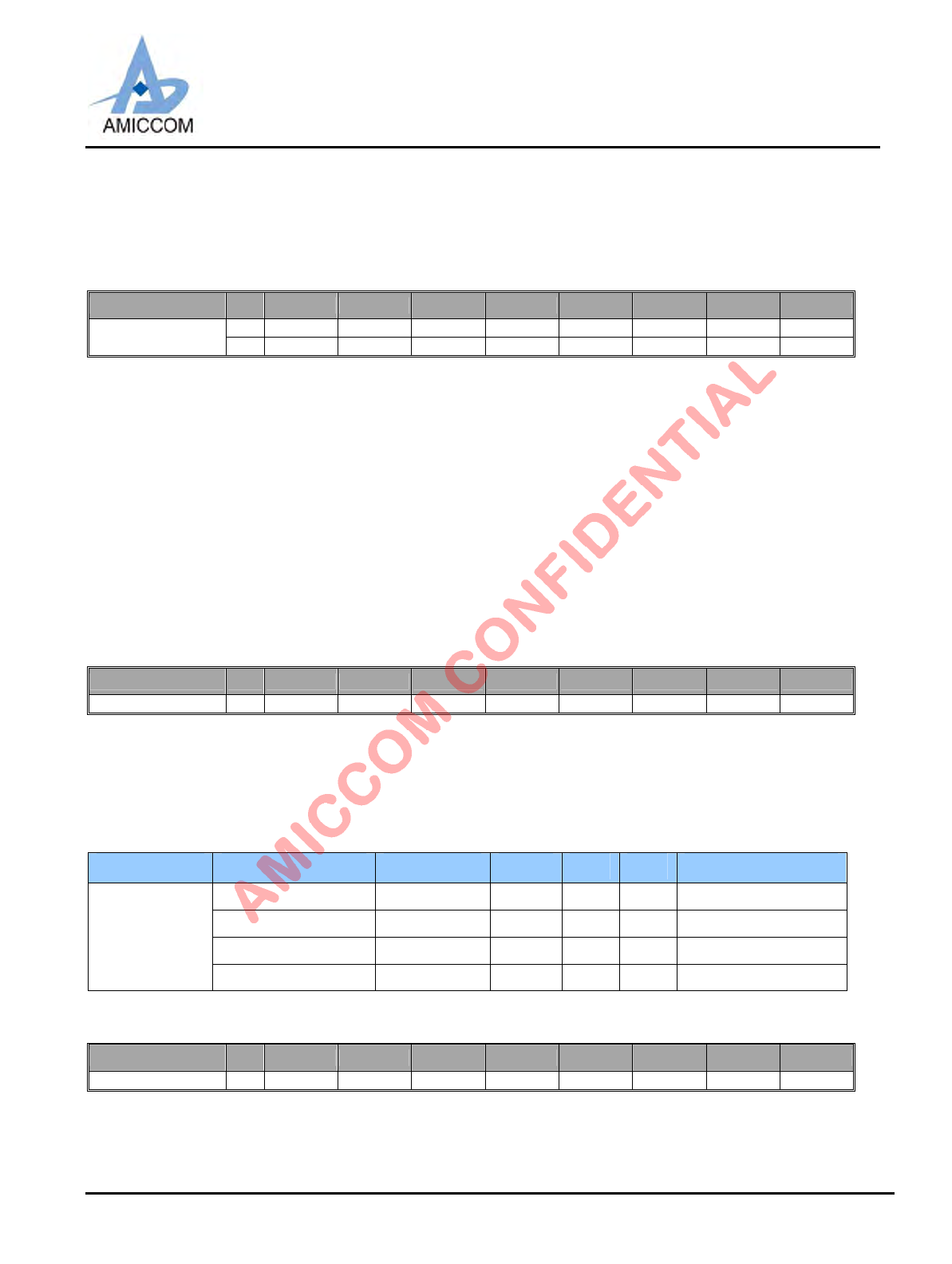
LBA7130
Oct., 2012, Version 0.6 (PRELIMINARY) 32 AMICCOM Electronics Corporation
DMV [1:0]: Demodulator D/A Voltage Range Select. Recommend DMV = [11].
[00]: 1/32*1.2. [01]: 1/16*1.2. [10]: 1/8*1.2. [11]: 1/4*1.2.
DEVFD [2:0]: VCO Modulation Data Delay by 8x over-sampling Clock. Recommend DEVFD = [011].
DEVD [2:0]: VCO Modulation Data Delay by XCPCK Clock. Recommend DEVD = [100].
9.2.45 Battery detect Register (Address: 2Ch)
Name R/W Bit 7 Bit 6 Bit 5 Bit 4 Bit 3 Bit 2 Bit 1 Bit 0
WLVR RGV1 RGV0 QDS BVT2 BVT1 BVT0 BD_E
Battery detect R-- RGV1 RGV0 BDF BVT2 BVT1 BVT0 BD_E
LVR: Low Power Bandgap Select. Recommend LVR = [1].
[0]: Disable. [1]: Enable.
RGV [1:0]: VDD_D and VDD_A voltage setting in non-Sleep mode. Recommend RGV = [11].
[00]: 2.1V. [01]: 2.0V. [10]: 1.9V. [11]: 1.8V.
QDS: VDD Quick Discharge Select. Recommend QDS = [1].
[0]: Disable. [1]: Enable.
BVT [2:0]: Battery voltage detect threshold.
[000]: 2.0V. [001]: 2.1V. [010]: 2.2V. [011]: 2.3V.
[100]: 2.4V. [101]: 2.5V. [110]: 2.6V. [111]: 2.7V.
BD_E: Battery Detect Enable.
[0]: Disable. [1]: Enable. It will be clear after battery detection is triggered.
BDF: Battery detection flag.
[0]: Battery voltage < BVT [2:0]. [1]: Battery voltage ≧ BVT [2:0].
9.2.46 TX test Register (Address: 2Dh)
Name R/W Bit 7 Bit 6 Bit 5 Bit 4 Bit 3 Bit 2 Bit 1 Bit 0
TX test W RMP1 RMP0 TXCS PAC1 PAC0 TBG2 TBG1 TBG0
RMP [1:0]: PA ramp up timing scale. Recommend RMP = [00].
TXCS: TX Current Setting. Recommend TXCS = [1].
[0]: lowest current. [1]: highest current.
PAC [1:0]: PA Current Setting.
TBG [2:0]: TX Buffer Setting.
RF Band Typical power (dBm) PWORS (24h) TBG TXCS PAC Typical current (mA)
5 1 7 1 2 29
0 1 0 1 0 20
-5 0 4 1 0 18
2.4GHz
-17 0 0 1 0 16
Refer to A7130 App. Note for more settings.
9.2.47 Rx DEM test Register I (Address: 2Eh)
Name R/W Bit 7 Bit 6 Bit 5 Bit 4 Bit 3 Bit 2 Bit 1 Bit 0
Rx DEM test I W DMT DCM1 DCM0 MLP1 MLP0 SLF2 SLF1 SLF0
DMT: Reserved for internal usage only. Shall be set to [0].
DCM [1:0]: Demodulator DC estimation mode. Recommend DCM = [10].
(The average length before hold is selected by DCL in RX DEM Test Register II.)
[00]: Fix mode (For testing only). DC level is set by DCV [7:0].

LBA7130
Oct., 2012, Version 0.6 (PRELIMINARY) 33 AMICCOM Electronics Corporation
[01]: Preamble hold mode. DC level is preamble average value.
[10]: ID hold mode. DC level is the average value hold about 8 bit data rate later if preamble is detected.
[11]: Payload average mode (For internal usage). DC level is payload data average.
MLP1: Reserved for internal usage. Shall set MLP1 = [0].
MLP0: Reserved for internal usage. Shall set MLP0 = [0].
SLF [2:0]: Symbol Recovery Loop Filter Setting. Shall be SLF[2:0] = [111].
9.2.48 Rx DEM test Register II (Address: 2Fh)
Name R/W Bit 7 Bit 6 Bit 5 Bit 4 Bit 3 Bit 2 Bit 1 Bit 0
Rx DEM test II W DCH1 DCH0 DCL2 DCL1 DCL0 RAW CDTM1 CDTM0
DCH [1:0]: DC Estimation of AGC hold mode. Recommend DCH = [11].
[00]: hold when PMDO. [01]: hold when Fsync. [10]: no hold. [11]: no hold.
DCL [2]: DC Estimation Average Length After ID Detected. Recommend DCL[2] = [1].
[0]: 128 bits. [1]: 256 bits.
DCL [1:0]: DC Estimation Average Length Before ID Detected. Recommend DCL[1:0] = [10].
[00]: 8 bits. [01]: 16 bits. [10]: 32 bits. [11]: 64 bits.
RAW: Raw Data Output Select. Recommend RAW = [1].
[0]: latch data output. [1]: RAW data output.
CDTM [1:0]: Preamble carrier detect setting. Recommend CDTM = [11].
[00]: 12. [01]: 24. [10]: 36. [11]: 48.
9.2.49 Charge Pump Current Register I (Address: 30h)
Name R/W Bit 7 Bit 6 Bit 5 Bit 4 Bit 3 Bit 2 Bit 1 Bit 0
CPC I WCPM3 CPM2 CPM1 CPM0 CPT3 CPT2 CPT1 CPT0
CPM [3:0]: Charge Pump Current Setting for VM loop. Recommend CPM = [1111].
Charge pump current = (CPM + 1) / 16 mA.
CPT [3:0]: Charge Pump Current Setting for VT loop. Recommend CPT = [0000].
Charge pump current = (CPT + 1) / 16 mA.
9.2.50 Charge Pump Current Register II (Address: 31h)
Name R/W Bit 7 Bit 6 Bit 5 Bit 4 Bit 3 Bit 2 Bit 1 Bit 0
CPC II WCPTX3 CPTX2 CPTX1 CPTX0 CPRX3 CPRX2 CPRX1 CPRX0
CPTX [3:0]: Charge Pump Current Setting for TX mode. Recommend CPTX = [0011].
Charge pump current = (CPTX + 1) / 16 mA.
CPRX [3:0]: Charge Pump Current Setting for RX mode. Recommend CPRX = [0111].
Charge pump current = (CPRX + 1) / 16 mA.
9.2.51 Crystal test Register (Address: 32h)
Name R/W Bit 7 Bit 6 Bit 5 Bit 4 Bit 3 Bit 2 Bit 1 Bit 0
Crystal test W CDPM CPS CPH CPCS DBD XCC XCP1 XCP0
CDPM:First Time Preamble Detect mode select. Recommend CDPM = [0].
CPS: PLL charge pump enable. Recommend CPS = [1].
[0]: Enable. [1]: Disable.
CPH: Charge Pump High Current. Shall be set to [0].
[0]: Normal. [1]: High.
CPCS: Charge Pump Current Select. Shall be set to [1].
[0]: Use CPM for TX, CPT for RX. [1]: Use CPTX for TX, CPRX for RX.
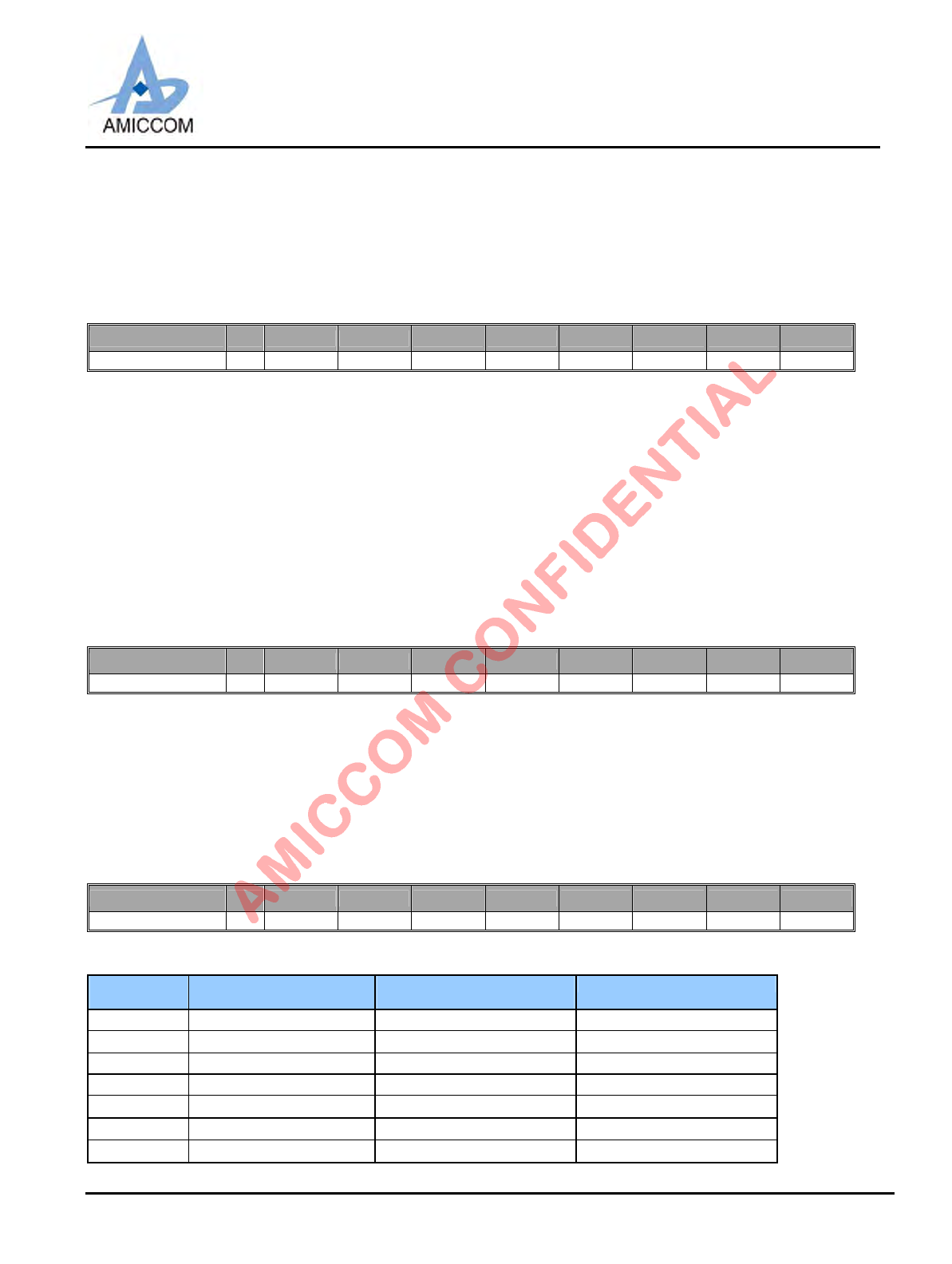
LBA7130
Oct., 2012, Version 0.6 (PRELIMINARY) 34 AMICCOM Electronics Corporation
DBD: Crystal Frequency Doubler High Level Pulse Width Select. Recommend DBD = [0].
[0]: about 8 ns. [1]: about 16 ns.
XCC: Crystal Startup Current Selection. Recommend XCC = [1].
[0]: about 0.7 mA. [1]: about 1.5 mA.
XCP [1:0]: Crystal Oscillator Regulated Couple Setting. Recommend XCP = [01].
[00]: 1.5mA. [01]: 0.5mA. [10]: 0.35mA. [11]: 0.3mA.
9.2.52 PLL test Register (Address:33h)
Name R/W Bit 7 Bit 6 Bit 5 Bit 4 Bit 3 Bit 2 Bit 1 Bit 0
PLL test W MDEN OLM PRIC1 PRIC0 PRRC1 PRRC0 SDPW NSDO
MDEN : Use for Manual VCO Calibration. Shall be set to [0].
OLM: Open Loop Modulation Enable. Shall be set to [0].
[0]: Disable. [1]: Enable.
PRIC [1:0]: Prescaler IF Part Current Setting. Shall be set to [01].
[00]: 0.95mA. [01]: 1.05mA. [10]: 1.15mA. [11]: 1.25mA.
PRRC [1:0]: Prescaler RF Part Current Setting. Shall be set to [01].
[00]: 1.0mA. [01]: 1.2mA. [10]: 1.4mA. [11]: 1.6mA.
SDPW: Clock Delay For Sigma Delta Modulator. Shall be set to [0].
[0]: 13 ns. [1]: 26 ns.
NSDO: Sigma Delta Order Setting. Shall be set to [1].
[0]: order 2. [1]: order 3.
9.2.53 VCO test Register I (Address:34h)
Name R/W Bit 7 Bit 6 Bit 5 Bit 4 Bit 3 Bit 2 Bit 1 Bit 0
VCO test I W DEVGD2 DEVGD1 DEVGD0 TLB1 TLB0 RLB1 RLB0 VBS
DEVGD [2:0]: Sigma Delta Modulator Data Delay Setting. Recommend DEVGD = [000].
TLB [1:0]: LO Buffer Current Select. Recommend TLB[1:0] = [10].
[00]: 0.6mA. [01]: 0.75mA. [10]: 0.9mA. [11]: 1.05mA.
RLB [1:0]: RF divider Current Select. Recommend RLB[1:0] = [10].
[00]: 1.2mA. [01]: 1.5mA. [10]: 1.8mA. [11]: 2.1mA.
VBCS : VCO Buffer Current Setting. Recommend VBCS = [1].
[0]: 1mA. [1]: 1.5mA.
9.2.54 RF Analog Test Register (Address: 35h)
Name R/W Bit 7 Bit 6 Bit 5 Bit 4 Bit 3 Bit 2 Bit 1 Bit 0
RFT W AGT3 AGT2 AGT1 AGT0 RFT3 RFT2 RFT1 RFT0
AGT[3:0]:Page selection for both DASP (2Ah) and ROMP (38h).
AGT[3:0]
(35h)
DASP Register Group
(2Ah)
ROMP Register Group
(38h)
Note
0DASP0 (page 0) ROMP0 (page 0) Internal usage only
1DASP1 (page 1) ROMP1 (page 1) Internal usage only
2 DADP2 (page 2) ROMP2 (page 2) Internal usage only
3DASP3 (page 3) ROMP3 (page 3) Internal usage only
4DASP4 (page 4) ROMP4 (page 4) Internal usage only
5DASP5 (page 5)
6 DASP6 (page 6)
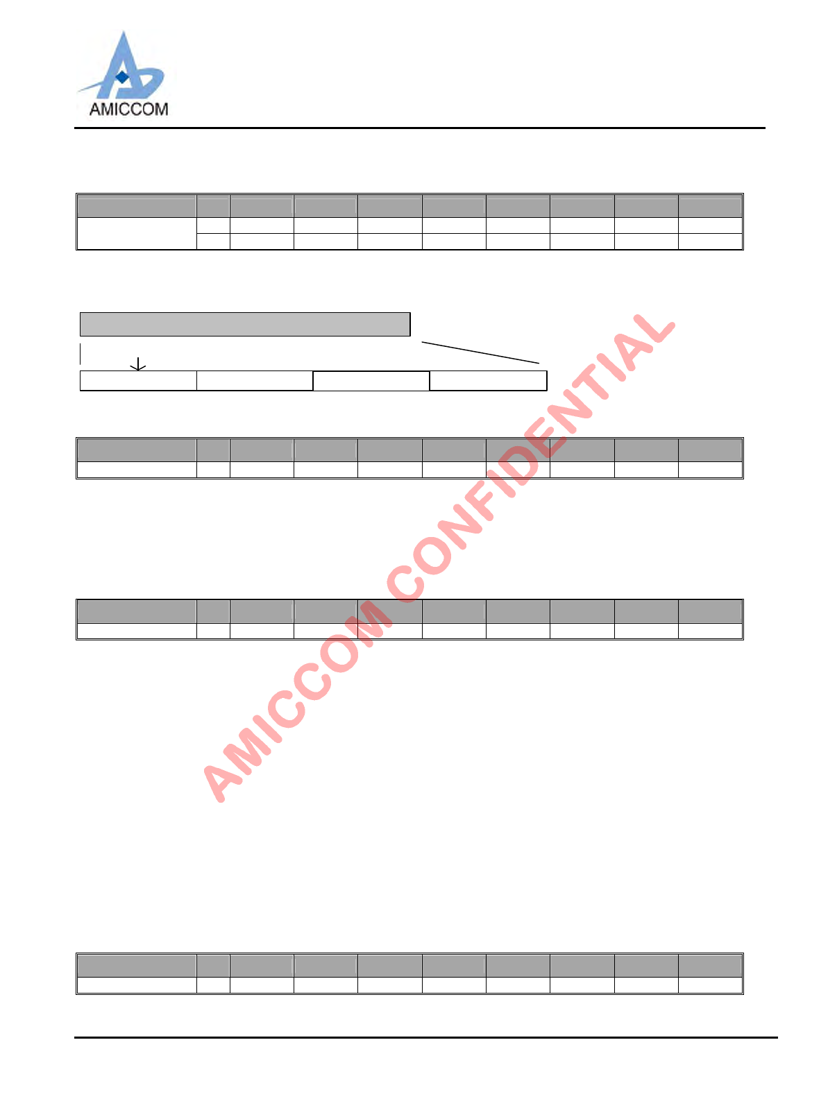
LBA7130
Oct., 2012, Version 0.6 (PRELIMINARY) 35 AMICCOM Electronics Corporation
RFT [3:0]: RF analog pin configuration for testing. Recommend RFT= [0000].
9.2.55 AES Key data Register (Address: 36h)
Name R/W Bit 7 Bit 6 Bit 5 Bit 4 Bit 3 Bit 2 Bit 1 Bit 0
RKEYO7 KEYO6 KEYO5 KEYO4 KEYO3 KEYO2 KEYO1 KEYO0
Key Data WKEYI7 KEYI6 KEYI5 KEYI4 KEYI3 KEYI2 KEYI1 KEYI0
KEYI [7:0]: AES128 key input, total 16-btyes. (Write only).
KEYO [7:0]: AES128 key output, total 16-bytes. (Read only). Select by KEYOS (3Eh).
A E S K e y D a ta (to ta l 1 6 B y te s )
KEY[7:0] KEY[15:8] …KEY[127:120]
9.2.56 Channel Select Register (Address: 37h)
Name R/W Bit 7 Bit 6 Bit 5 Bit 4 Bit 3 Bit 2 Bit 1 Bit 0
Channel Select WCHI3 CHI2 CHI1 CHI0 CHD3 CHD2 CHD1 CHD0
CHI [3:0]: Auto IF Offset Channel Number Setting. Recommend CHI [3:0] = [0111].
FCHSP × (CHI + 1 ) = FIF
Refer to chapter 14 for FCHSP setting.
CHD [3:0]: Channel Frequency Offset for Deviation Calibration. Recommend CHD [3:0] = [0111].
Offset channel number = +/- (CHD + 1).
9.2.57 ROMP0 (Address: 38h, Page 0 by AGT[3:0]=0)
Name R/W Bit 7 Bit 6 Bit 5 Bit 4 Bit 3 Bit 2 Bit 1 Bit 0
ROMP0 WMPOR EPRG MIGS MRGS MRSS MTMS MADS MBGS
MPOR: manual SPI read in OTP program cycle.
EPRG: enable OTP program in test mode.
[0]: disable. [1]: enable.
MIGS: IF gain setting select.
[0]: SPI setting. [1]: OTP setting.
MRGS: LNA and mixer gain setting select.
[0]: SPI setting. [1]: OTP setting.
MRSS: RSSI voltage fine trim setting select.
[0]: SPI setting. [1]: OTP setting.
MTMS: Temp voltage fine trim setting select.
[0]: SPI setting. [1]: OTP setting.
MADS: ADC fine trim setting select.
[0]: SPI setting. [1]: OTP setting.
MBGS: Bandgap voltage fine trim setting select.
[0]: SPI setting. [1]: OTP setting.
9.2.57 ROMP1 (Address: 38h, Page 1 by AGT[3:0]=1)
Name R/W Bit 7 Bit 6 Bit 5 Bit 4 Bit 3 Bit 2 Bit 1 Bit 0
ROMP1 WAPG MPA1 MPA0 FBG4 FBG3 FBG2 FBG1 FBG0
APG: OTP program select.
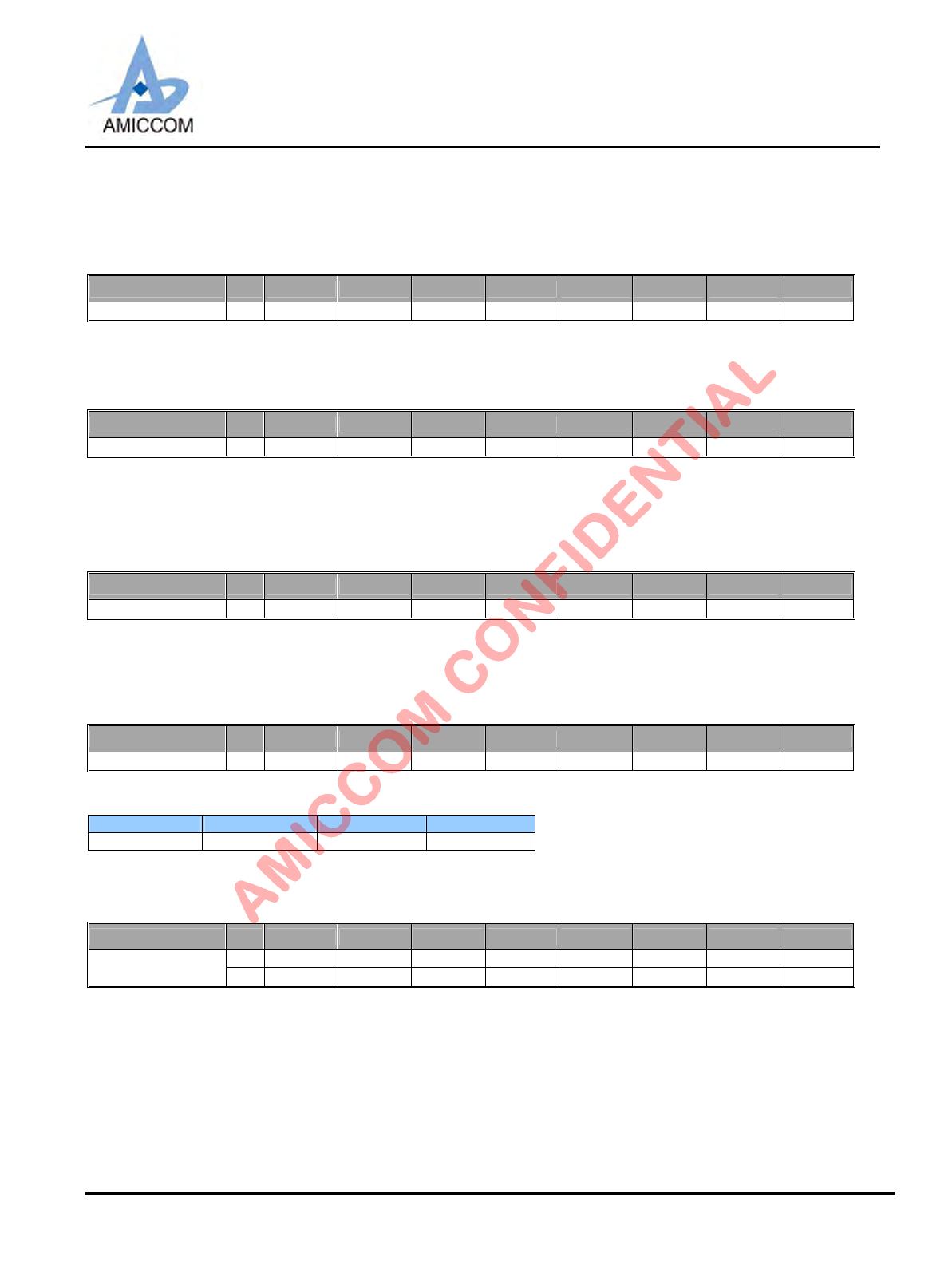
LBA7130
Oct., 2012, Version 0.6 (PRELIMINARY) 36 AMICCOM Electronics Corporation
[1]: auto program. [0]: manual SPI setting.
MPA [1:0]: OPT address setting in manual SPI OTP program.
FBG [4:0]: Bandgap voltage SPI fine trim setting.
9.2.57 ROMP2 (Address: 38h, Page 2 by AGT[3:0]=2)
Name R/W Bit 7 Bit 6 Bit 5 Bit 4 Bit 3 Bit 2 Bit 1 Bit 0
ROMP2 WPTM1 PTM0 CTR5 CTR4 CTR3 CTR2 CTR1 CTR0
PTM [1:0]: OTP program operation mode select. Recommend PTM = [00].
CTR [5:0]: ADC voltage SPI fine trim setting.
9.2.57 ROMP3 (Address: 38h, Page 3 by AGT[3:0]=3)
Name R/W Bit 7 Bit 6 Bit 5 Bit 4 Bit 3 Bit 2 Bit 1 Bit 0
ROMP3 WFGC1 FGC0 CRS2 CRS1 CRS0 SRS2 SRS1 SRS0
FGC[1:0]: BPF fine gain control.
CRS [2:0]: RSSI voltage offset fine trim setting.
SRS [2:0]: RSSI voltage curve slope fine time setting.
9.2.57 ROMP4 (Address: 38h, Page 4 by AGT[3:0]=4)
Name R/W Bit 7 Bit 6 Bit 5 Bit 4 Bit 3 Bit 2 Bit 1 Bit 0
ROMP4 W-- STMP STM5 STM4 STM3 STM2 STM1 STM0
STMP: Temp voltage ADC reading select.
[0]: 1 scale / degree C. [1]: 2 scale/degree C.
STM [5:0]: Temperature voltage SPI fine trim setting.
9.2.58 Data Rate Clock Register (Address: 39h)
Name R/W Bit 7 Bit 6 Bit 5 Bit 4 Bit 3 Bit 2 Bit 1 Bit 0
Data Rate Clock WSDR7 SDR6 SDR5 SDR4 SDR3 SDR2 SDR1 SDR0
SDR [1:0]: Data Rate Setting. On-air Data rate = FIF / (SDR+1).
Data Rate FIF (Hz) SDR [7:0] Xtal
4M 4M 0x00 16 MHz
Please refer to chapter 13 for details.
9.2.59 FCR Register (Address: 3Ah)
Name R/W Bit 7 Bit 6 Bit 5 Bit 4 Bit 3 Bit 2 Bit 1 Bit 0
RARTEF VPOAK RCR3 RCR2 RCR1 RCR0 EAK EAR
FCR WFCL1 FCL0 ARC3 ARC2 ARC1 ARC0 EAK EAR
FCL [1:0] : FCB Length.
[00]: No Frame Control.
[01]: 1 byte FCB (3Dh).
[10]: 2 byte FCB (3Dh).
[11]: 4 byte FCB (3Dh).
Please refer to chapter 16 and 19 for details.
ARC [3:0] : Auto Resend Cycle Setting.
[0000]: resend disable.
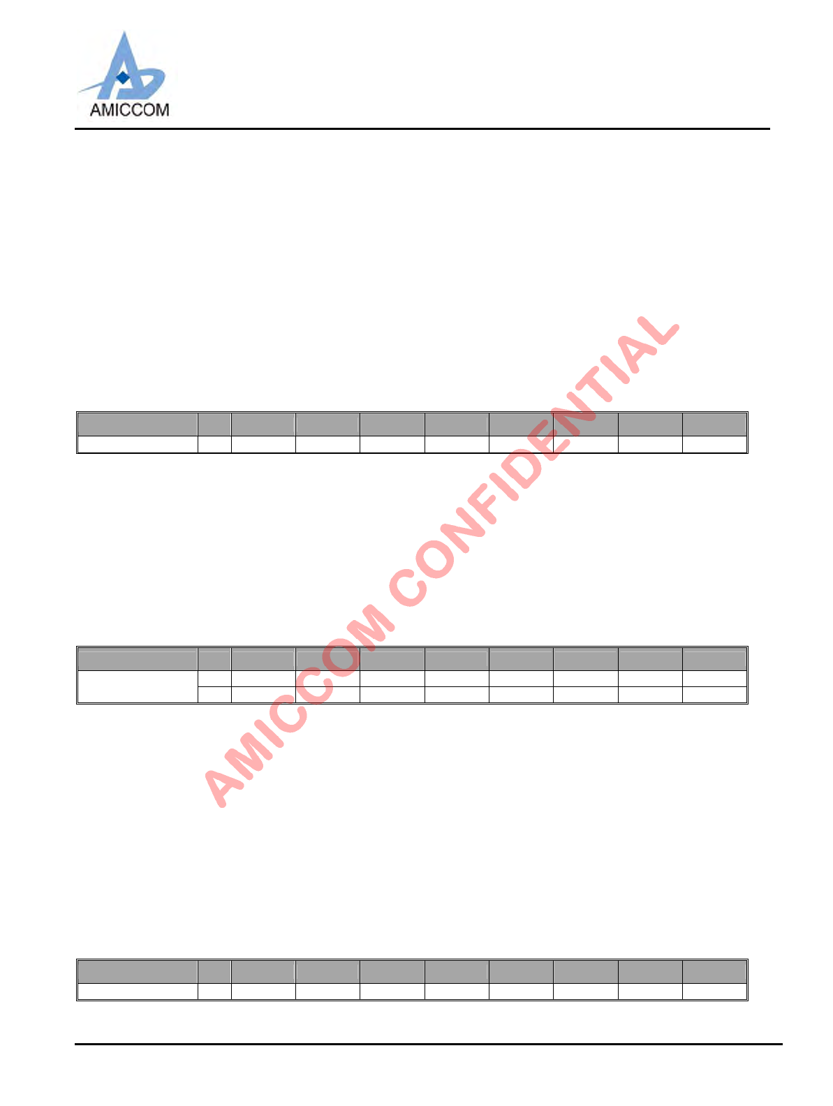
LBA7130
Oct., 2012, Version 0.6 (PRELIMINARY) 37 AMICCOM Electronics Corporation
[0001]: 1[0010]: 2[0011]: 3[0100]: 4 [0101]: 5[0110]: 6[0111]: 7 [1000]: 8[1001]: 9[1010]: 10
[1011]: 11 [1100]: 12 [1101]: 13 [1110]: 14 [1111]: 15
EAK : Enable Auto ACK.
[0]: Disable. [1]: Enable.
EAR : Enable Auto Resend.
[0]: Disable. [1]: Enable.
ARTEF: Auto re-transmission ending flag (read only).
[0]: Resend not end [1 ]: Finish resend.
VPOAK : Valid Packet or ACK OK Flag. (read only and auto clear by Strobe command)
[0]: Neither valid packet nor ACK OK. [1]: Valid packet or ACK OK.
RCR [3:0] (read) : Decremented of ARC[3:0].
Please refer to chapter 16 and 19 for details.
9.2.60 ARD Register (Address: 3Bh)
Name R/W Bit 7 Bit 6 Bit 5 Bit 4 Bit 3 Bit 2 Bit 1 Bit 0
ARD WARD7 ARD6 ARD5 ARD4 ARD3 ARD2 ARD1 ARD0
ARD[7:0] : Auto Resend Delay
ARD Delay = 200 us * (ARD+1) à (200us ~ 51.2 ms)
[0000-0000]: 200 us.
[0000-0001]: 400 us.
[0000-0010]: 600 us.
…
…
[1111-1111]: 51.2 ms.
Please refer to chapter 19 for details.
9.2.61 AFEP Register (Address: 3Ch)
Name R/W Bit 7 Bit 6 Bit 5 Bit 4 Bit 3 Bit 2 Bit 1 Bit 0
R 0 0 EARTS2 EARTS1 EARTS0 SID2 SID1 SID0
AFEP WEAF SPSS ACKFEP5 ACKFEP4 ACKFEP3 ACKFEP2 ACKFEP1 ACKFEP0
EAF: Enable ACK FIFO.
[0]: Disable. [1]: Enable.
SPSS : Mode Back Select for Auto ACK/Resend.
[0]: Standby mode. [1]: PLL mode.
ACKFEP [5:0]: FIFO Length setting for auto-ack packet.
ACK FIFO Length = (ACKFEP[5:0] + 1)
max. 64 bytes.
EARTS [2:0]: Enable Auto Resend Read.
SID [2:0]: Serial Packet ID.
This device increases SID each time for every new packet and keep the same SID when retransmitting.
Please refer to chapter 16 and 19 for details.
9.2.62 FCB Register (Address: 3Dh)
Name R/W Bit 7 Bit 6 Bit 5 Bit 4 Bit 3 Bit 2 Bit 1 Bit 0
FCB R/W F7 F6 F5 F4 F3 F2 F1 F0
FCB [7:0]: Frame Control Buffer, total 20-bytes.
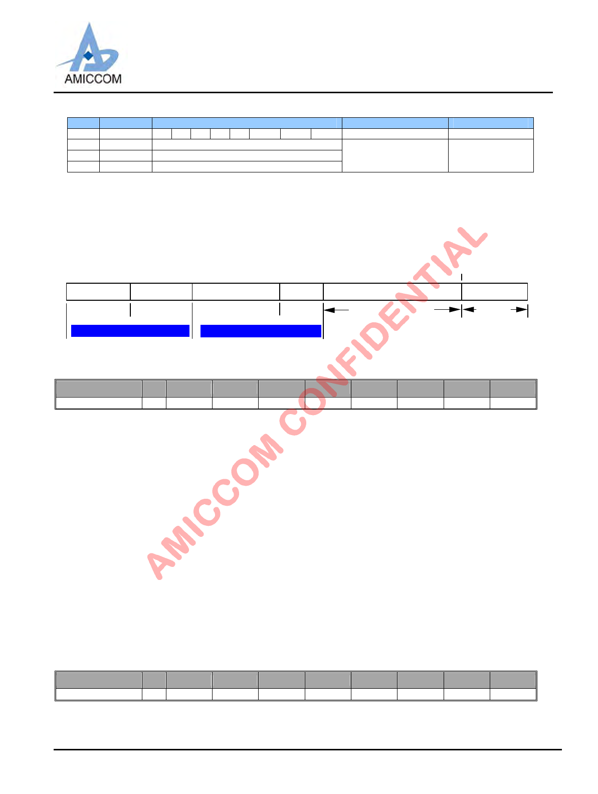
LBA7130
Oct., 2012, Version 0.6 (PRELIMINARY) 38 AMICCOM Electronics Corporation
Byte Name Bit-Map Description Strobe Cmd
0FCB0 0 0 1 1 1 SID2 SID1 SID0 For auto-resend. NA
1FCB1 [7:0]
2FCB2 [7:0]
3FCB3 [7:0]
ACK info
by user’s attaching
NA
Remark:
1. Please refer to section 10.4.10 for details.
2. SID is auto incremental for every new packet if FCB0 is enabled.
3. FCB0 ~ FCB3 is controlled by FCL[1:0] (3Ah)
4. User can attach wanted ACK information to FCB1 ~ FCB3 if auto-ack is enabled (EAK =1).
Please refer to chapter 16 and 19 for details.
ID codePreamble Payload (CRC)
4 bytes 4 bytes 2 bytesPhy. 64 bytes
FCB
1~4 bytes
FEP
12 bits
au to
ack/resend
dynamic
FIFO
M A C H eader (self-generated)PH Y H eader (self-generated)
9.2.63 KEYC Register (Address: 3Eh)
Name R/W Bit 7 Bit 6 Bit 5 Bit 4 Bit 3 Bit 2 Bit 1 Bit 0
KEYC WKEYOS AFIDS ARTMS MIDS AESS -- AKFS EDCRS
KEYOS: AES128 Key source read select.
[0]: If AKFS=1, from RX received encrypted AES128 key data.
If AKFS=0, from SPI write AES128 key data.
[1]: From encrypted/decrypted AES128 key data.
Please refer to chapter 21 for details.
AFIDS: FIFO ID appendixes Select.
[0]: Disable. [1]: Enable.
ARTMS: auto-resend Interval Mode Select.
[0]: random interval. [1]: fixed interval.
Please refer to chapter 16 and 19 for details.
MIDS: FIFO control byte address mapping for FIFO ID select.
[0]: Received device ID. [1]: internal FIFO control byte ID.
AESS: encryption format selection.
[1]: Standard AES 128 bit. [0]: proprietary 32 bit.
Please refer to chapter 21 for details.
AKFS: Data packet with decrypted key appendixes select.
[0]: Disable. [1]: Enable.
EDRCS: Data encrypt or decrypt select.
[0]: Disable. [1]: Enable.
9.2.64 USID Register (Address: 3Fh)
Name R/W Bit 7 Bit 6 Bit 5 Bit 4 Bit 3 Bit 2 Bit 1 Bit 0
USID WRND7 RND6 RND5 RND4 RND3 RND2 RND1 RND0
RND [7:0]: Random seed for auto-resend interval.
Please refer to chapter 16 and 19 for details.
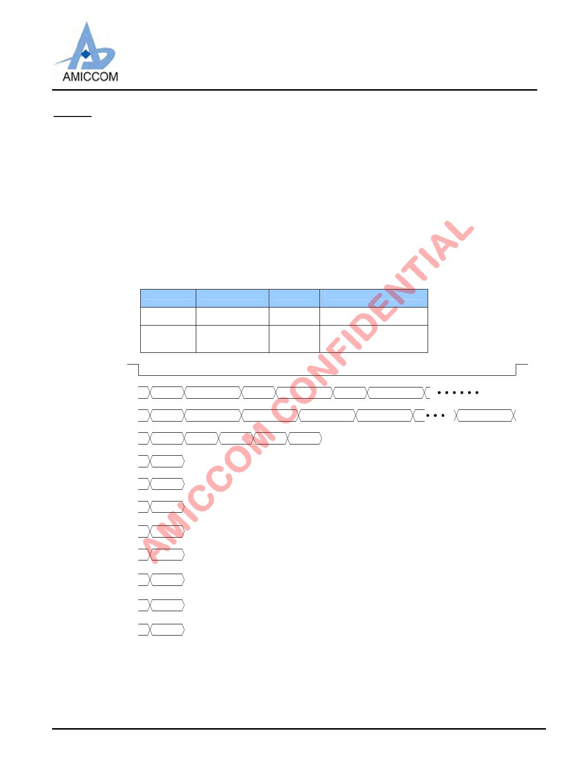
LBA7130
Oct., 2012, Version 0.6 (PRELIMINARY) 39 AMICCOM Electronics Corporation
10. SPI
A7130 only supports one SPI interface with maximum data rate up to 15Mbps. MCU should assert SCS pin low (SPI chip
select) to active accessing of A7130. Via SPI interface, user can access control registers and issue Strobe command.
Figure 10.1 gives an overview of SPI access manners.
3-wire SPI (SCS, SCK and SDIO) or 4-wire SPI (SCS, SCK, SDIO and GIO1/GIO2) configuration is provided. For 3-wire SPI,
SDIO pin is configured as bi-direction to be data input and output. For 4-wire SPI, SDIO pin is data input and GIO1 (or GIO2)
pin is data output. In such case, GIO1S (0bh) or GIO2S (0ch) should be set to [0110].
For SPI write operation, SDIO pin is latched into A7130 at the rising edge of SCK. For SPI read operation, if input address is
latched by A7130, data output is aligned at falling edge of SCK. Therefore, MCU can latch data output at the rising edge of
SCK.
To control A7130’s internal state machine, it is very easy to send Strobe command via SPI interface. The Strobe command is
a unique command set with total 8 commands. See section 10.3, 10.4 and 10.5 for details.
SPI chip select Data In Data Out
3-Wire SPI SCS pin = 0 SDIO pin SDIO pin
4-Wire SPI SCS pin = 0 SDIO pin GIO1 (GIO1S=0110) /
GIO2 (GIO2S=0110)
ADDRreg DataByte ADDRreg ADDRreg
ADDRFIFO DataByte0DataByte1DataByte2DataByte3
ADDRID DataByte0DataByte1DataByte2DataByte3
Strobe
CommandSleep Mode
Sleep Mode
Read/Write ID
register
Read/Write RF
FIFO
Read/Write register
SCS
DataByten
DataByte DataByte
Strobe
CommandIdle Mode
Idle Mode
Strobe
CommandSTBY Mode
STBY Mode
Strobe
CommandPLL Mode
PLL Mode
Strobe
CommandRX Mode
RX Mode
Strobe
CommandTX Mode
TX Mode
Strobe
CommandFIFO Write Reset
FIFO Write Reset
Strobe
CommandFIFO Read Reset
FIFO Read Reset
Figure 10.1 SPI Access Manners
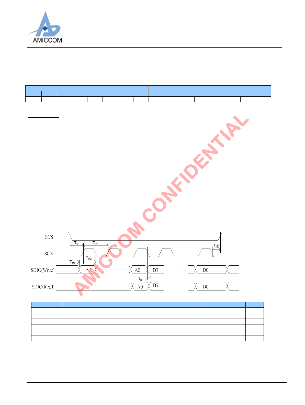
LBA7130
Oct., 2012, Version 0.6 (PRELIMINARY) 40 AMICCOM Electronics Corporation
10.1 SPI Format
The first bit (A7) is critical to indicate A7130 the following instruction is “Strobe command” or “control register”. See Table 10.1
for SPI format. Based on Table 10.1, To access control registers, just set A7=0, then A6 bit is used to indicate read (A6=1) or
write operation (A6=0). See Figure 10.2 (3-wire SPI) and Figure 10.3 (4-wire SPI) for details.
Address Byte (8 bits) Data Byte (8 bits)
CMD R/W Address Data
A7 A6 A5 A4 A3 A2 A1 A0 7 6 5 4 3 2 1 0
Table 10.1 SPI Format
Address byte:
Bit 7: Command bit
[0]: Control registers.
[1]: Strobe command.
Bit 6: R/W bit
[0]: Write data to control register.
[1]: Read data from control register.
Bit [5:0]: Address of control register
Data Byte:
Bit [7:0]: SPI input or output data, see Figure 10.2 and Figure 10.3 for details.
10.2 SPI Timing Characteristic
No matter 3-wire or 4-wire SPI interface is configured, the maximum SPI data rate is 10 Mbps. To active SPI interface, SCS
pin must be set to low. For correct data latching, user has to take care hold time and setup time between SCK and SDIO. See
Table 10.2 for SPI timing characteristic.
Parameter Description Min. Max. Unit
FCFIFO clock frequency. 10 MHz
TSE Enable setup time. 50 ns
THE Enable hold time. 50 ns
TSW TX Data setup time. 50 ns
THW TX Data hold time. 50 ns
TDR RX Data delay time. 0 50 ns
Table 10.2 SPI Timing Characteristic
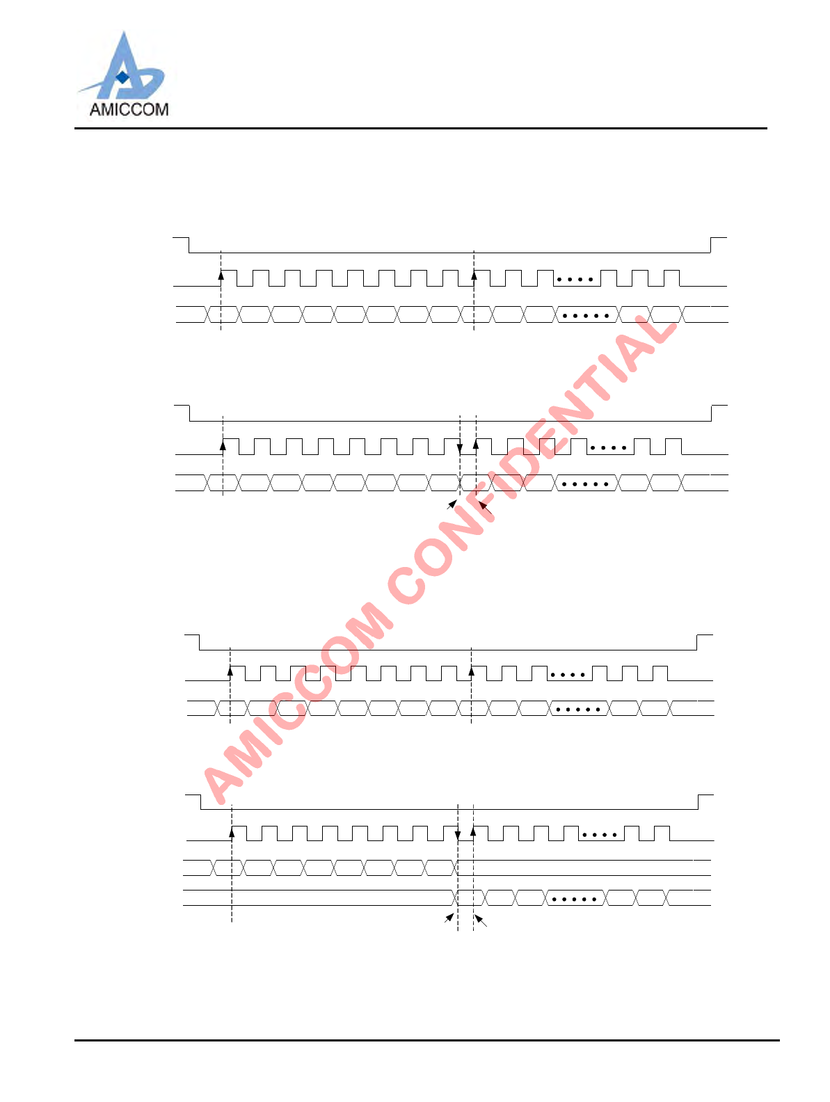
LBA7130
Oct., 2012, Version 0.6 (PRELIMINARY) 41 AMICCOM Electronics Corporation
10.3 SPI Timing Chart
In this section, 3-wire and 4-wire SPI interface read / write timing are described.
10.3.1 Timing Chart of 3-wire SPI
A7 DW7A0A1A2A3A4A5A6 DW0DW5DW6 DW1
SCS
SCK
SDIO
SCK
SCS
A7 DR7A0A1A2A3A4A5A6 DR0DR5DR6 DR1
SDIO
RF IC will latch address bit at
rising edge of SCK
RF IC will latch data bit at
the rising edge of SCK
RF IC will latch address bit at
rising edge of SCK
3-Wire serial interface - Write operation
3-Wire serial interface - Read operation
RF IC will change the data
when falling edge of SCK
MCU can latch data at rising
edge of SCK
Figure 10.2 Read/Write Timing Chart of 3-Wire SPI
10.3.2 Timing Chart of 4-wire SPI
A7 DW7A0A1A2A3A4A5A6 DW0DW5DW6 DW1
SCS
SCK
SDIO
SCK
SCS
RF IC will latch address bit at
rising edge of SCK
RF IC will latch data bit at rising
edge of SCK
RF IC will latch address bit at
rising edge of SCK
4-Wire serial interface - Write operation
4-Wire serial interface - Read operation
RF IC will change the data
when falling edge of SCK
MCU can latch data at the
rising edge of SCK
GIOx DR7 DR1D
R
0D
R
5D
R
6 D
R
2
SDI A7 A0A1A2A3A4A5A6 x
x
Figure 10.3 Read/Write Timing Chart of 4-Wire SPI
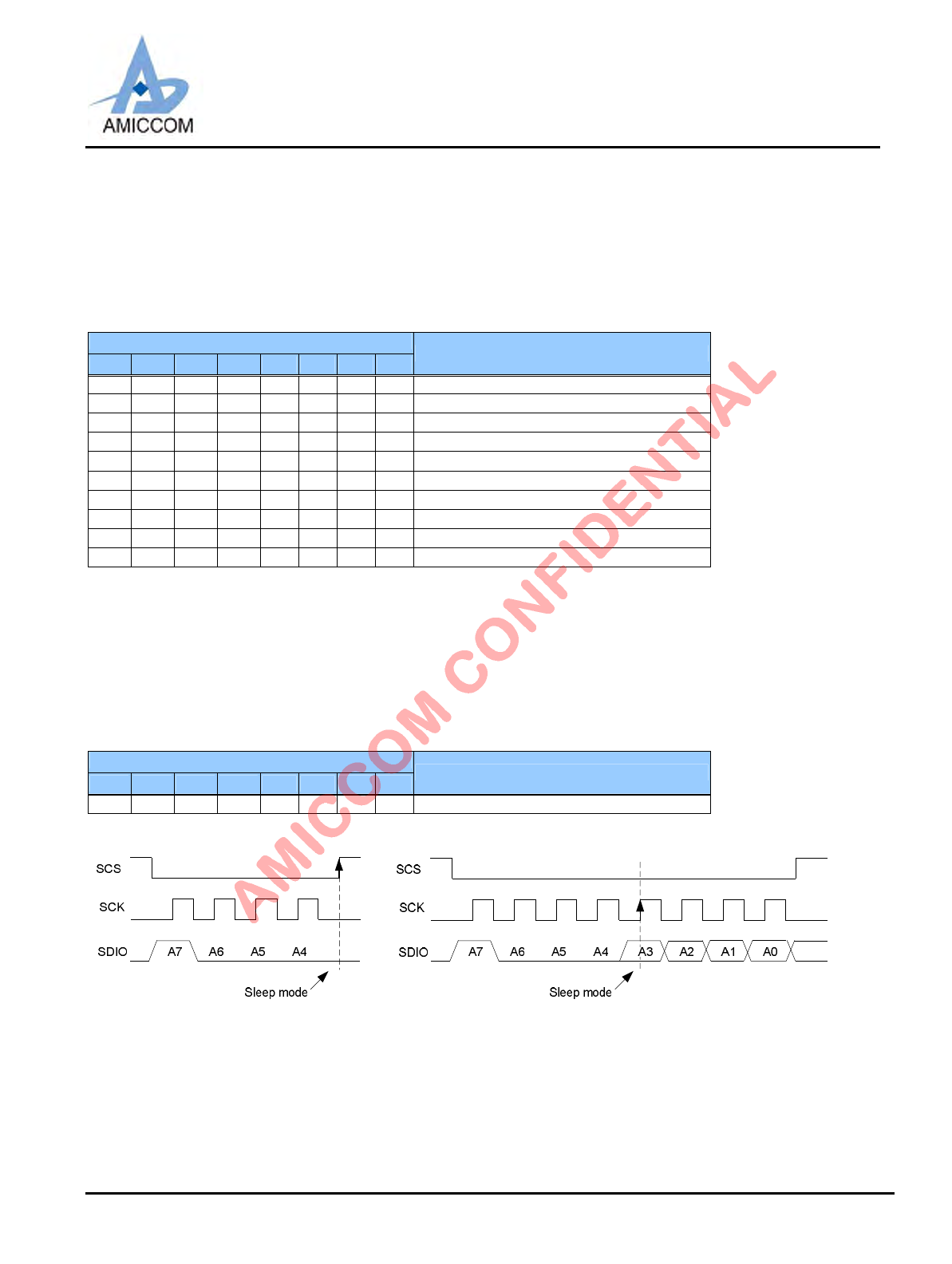
LBA7130
Oct., 2012, Version 0.6 (PRELIMINARY) 42 AMICCOM Electronics Corporation
10.4 Strobe Commands
A7130 supports 8 Strobe commands to control internal state machine for chip’s operations. Table 10.3 is the summary of
Strobe commands.
Be notice, Strobe command could be defined by 4-bits (A7~A4) or 8-bits (A7~A0). If 8-bits Strobe command is selected, A3
~ A0 are don’t care conditions. In such case, SCS pin can be remaining low for asserting next commands.
Strobe Command when AFIDS =0 (3Eh) and MIDS =0 (3Eh)
Strobe Command
A7 A6 A5 A4 A3 A2 A1 A0 Description
1 0 0 0 1 0 0 0 Deep Sleep mode (I/Os are in tri-state)
1 0 0 0 1 0 1 1 Deep Sleep mode (I/Os are pulled high)
1 0 0 0 x x x x Sleep mode
1 0 0 1 x x x x Idle mode
1 0 1 0 x x x x Standby mode
1 0 1 1 x x x x PLL mode
1 1 0 0 x x x x RX mode
1 1 0 1 x x x x TX mode
1 1 1 0 x x x x FIFO write pointer reset
1 1 1 1 x x x x FIFO read pointer reset
Remark: x means “ don’t care”
Table 10.3 Strobe Commands by SPI interface
10.4.1 Strobe Command - Sleep Mode
Refer to Table 10.3 user can issue 4 bits (1000) Strobe command directly to set A7130 into Sleep mode. Below are the
Strobe command table and timing chart.
Strobe Command
Strobe Command
A7 A6 A5 A4 A3 A2 A1 A0 Description
1 0 0 0 x X x x Sleep mode
Figure 10.4 Sleep mode Command Timing Chart
10.4.2 Strobe Command - ldle Mode
Refer to Table 10.3, user can issue 4 bits (1001) Strobe command directly to set A7130 into Idle mode. Below is t he Strobe
command table and timing chart.
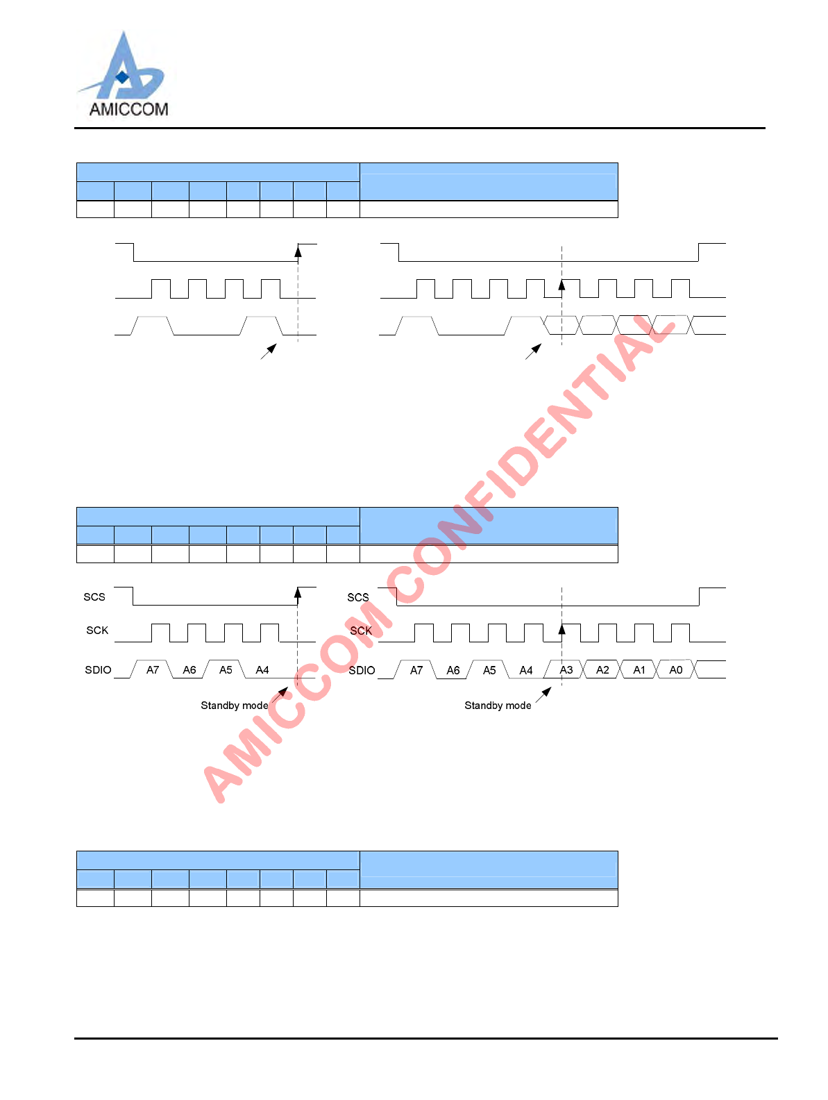
LBA7130
Oct., 2012, Version 0.6 (PRELIMINARY) 43 AMICCOM Electronics Corporation
Strobe Command
Strobe Command
A7 A6 A5 A4 A3 A2 A1 A0 Description
1 0 0 1 x X x x Idle mode
SCS
SCK
SDIO
Idle mode
A7 A4A5A6
SCS
SCK
SDIO
Idle mode
A7 A4A5A6 A3 A0A1A2
Figure 10.5 Idle mode Command Timing Chart
10.4.3 Strobe Command - Standby Mode
Refer to Table 10.3, user can issue 4 bits (1010) Strobe command directly to set A7130 into Standby mode. Below is the
Strobe command table and timing chart.
Strobe Command
Strobe Command
A7 A6 A5 A4 A3 A2 A1 A0 Description
1 0 1 0 x X x x Standby mode
Figure 10.6 Standby mode Command Timing Chart
10.4.4 Strobe Command - PLL Mode
Refer to Table 10.3, user can issue 4 bits (1011) Strobe command directly to set A7130 into PLL mode. Below are the
Strobe command table and timing chart.
Strobe Command
Strobe Command
A7 A6 A5 A4 A3 A2 A1 A0 Description
1 0 1 1 x X x x PLL mode
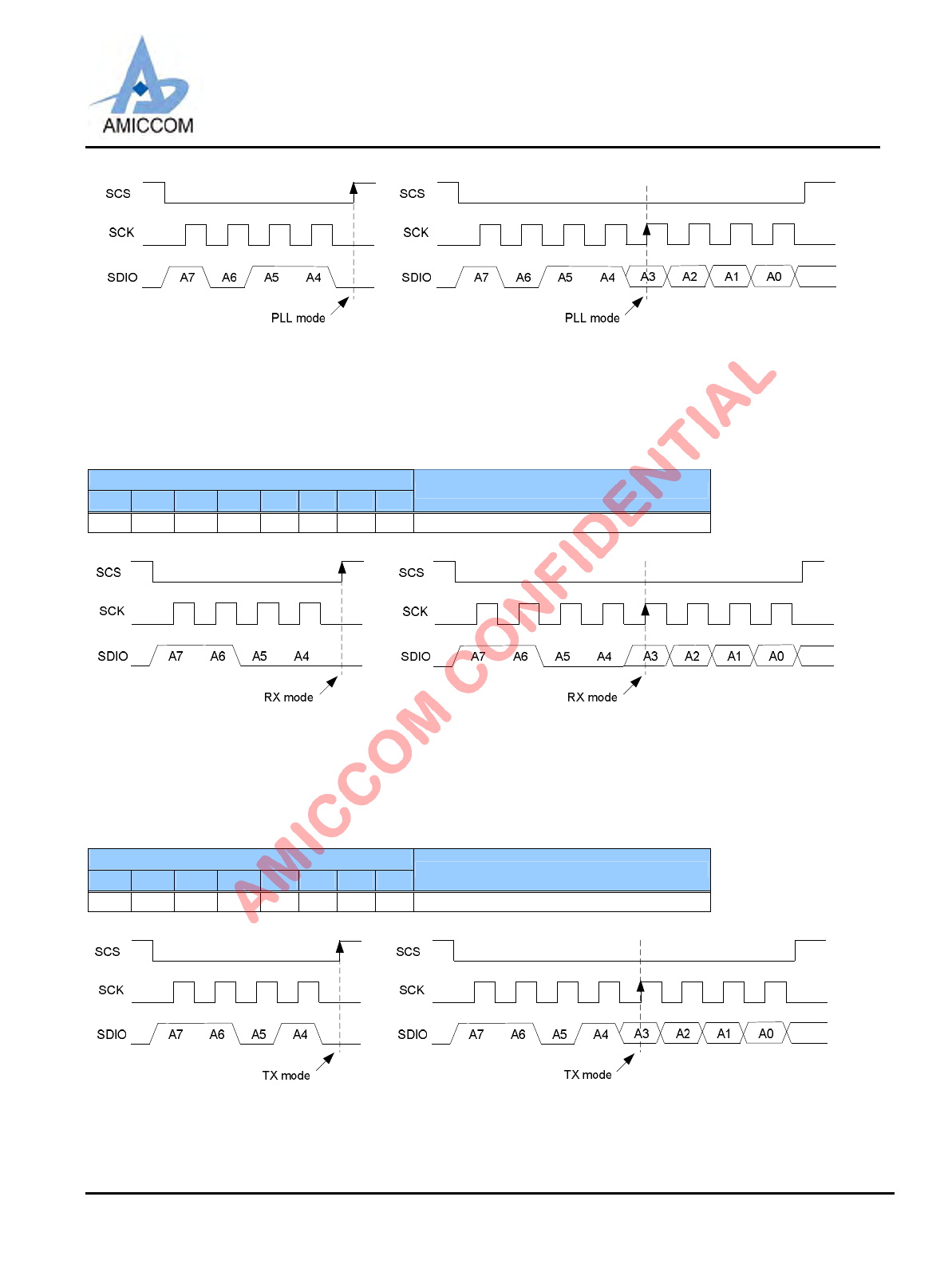
LBA7130
Oct., 2012, Version 0.6 (PRELIMINARY) 44 AMICCOM Electronics Corporation
Figure 10.7 PLL mode Command Timing Chart
10.4.5 Strobe Command - RX Mode
Refer to Table 10.3, user can issue 4 bits (1100) Strobe command directly to set A7130 into RX mode. Below are the Strobe
command table and timing chart.
Strobe Command
Strobe Command
A7 A6 A5 A4 A3 A2 A1 A0 Description
1 1 0 0 x X x x RX mode
Figure 10.8 RX mode Command Timing Chart
10.4.6 Strobe Command - TX Mode
Refer to Table 10.3, user can issue 4 bits (1101) Strobe command directly to set A7130 into TX mode. Below are the Strobe
command table and timing chart.
Strobe Command
Strobe Command
A7 A6 A5 A4 A3 A2 A1 A0 Description
1 1 0 1 x x x x TX mode
Figure 10.9 TX mode Command Timing Chart
10.4.7 Strobe Command – FIFO Write Pointer Reset
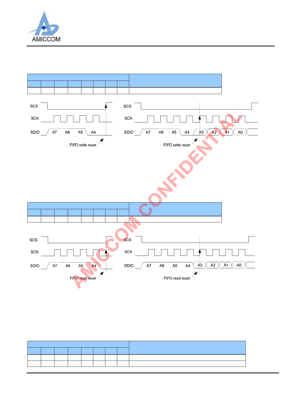
LBA7130
Oct., 2012, Version 0.6 (PRELIMINARY) 45 AMICCOM Electronics Corporation
Refer to Table 10.3, user can issue 4 bits (1110) Strobe command directly to reset A7130 FIFO write pointer. Below is the
Strobe command table and timing chart.
Strobe Command
Strobe Command
A7 A6 A5 A4 A3 A2 A1 A0 Description
1 1 1 0 x x x x FIFO write pointer reset
Figure 10.10 FIFO write pointer reset Command Timing Chart
10.4.8 Strobe Command – FIFO Read Pointer Reset
Refer to Table 10.3, user can issue 4 bits (1111) Strobe command directly to reset A7130 FIFO read pointer. Below are the
Strobe command table and timing chart.
Strobe Command
Strobe Command
A7 A6 A5 A4 A3 A2 A1 A0 Description
1 1 1 1 x x x x FIFO read pointer reset
Figure 10.11 FIFO read pointer reset Command Timing Chart
10.4.9 Strobe Command – Deep Sleep Mode
Refer to Table 10.3, user can issue (8 bits) deep sleep Strobe command directly to switch off power supply to A7130.In this
mode, A7130 is staying minimum current consumption. All registers are no data retention and re-calibration flow is
necessary. Below are the Strobe command table and timing chart.
Strobe Command
Strobe Command
A7 A6 A5 A4 A3 A2 A1 A0 Description
1 0 0 0 1 0 0 0 Tri-state of GIO1 / GIO2 (no register retention)
1 0 0 0 1 0 1 1 Internal Pull-High of GIO1 / GIO2 (no register retention)
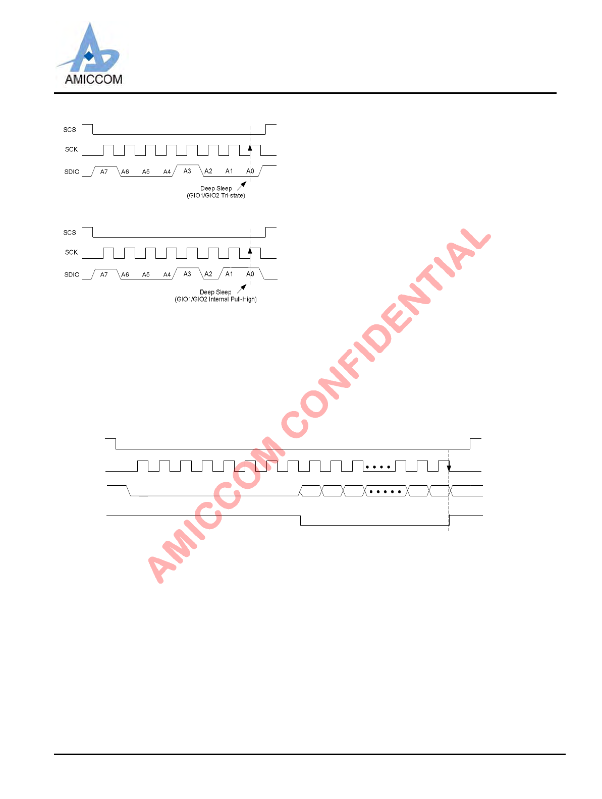
LBA7130
Oct., 2012, Version 0.6 (PRELIMINARY) 46 AMICCOM Electronics Corporation
Figure 10.12 Deep Sleep Mode Timing Chart
10.5 Reset Command
In addition to power on reset (POR), MCU could issue software reset to A7130 by setting Mode Register (00h) through SPI
interface as shown below. As long as 8-bits address (A7~A0) are delivered zero and data (D7~D0) are delivered zero, A7130
is informed to generate internal signal “RESETN” to initial itself. After reset command, A7130 is in standby mode and
calibration procedure shall be issued again.
A7 DW7A0A1A2A3A4A5A6 DW0DW5DW6 DW1
SCS
SCK
SDIO
Reset RF chip
RESETN
Figure 10.14 Reset Command Timing Chart
10.6 ID Accessing Command
A7130 has built-in 32-bits ID Registers for customized identification code. It is accessed via SPI interface. ID length is
recommended to be 32 bits by setting IDL (1Fh). Therefore, user can toggle SCS pin to high to terminate ID accessing
command when ID data is output completely.
Figure 10.13 and 10.14 are timing charts of 32-bits ID accessing via 3-wire SPI.
10.6.1 ID Write Command
User can refer to Figure 10.2 for SPI write timing chart in details. Below is the procedure of ID write command.
Step1: Deliver A7~A0 = 00000110 (A6=0 for write, A5~A0 = 000110 for ID addr, 06h).
Step2: By SDIO pin, deliver 32-bits ID into A7130 in sequence by Data Byte 0 (recommend 5xh or Axh), 1, 2 and 3.
Step3: Toggle SCS pin to high when step2 is completed.
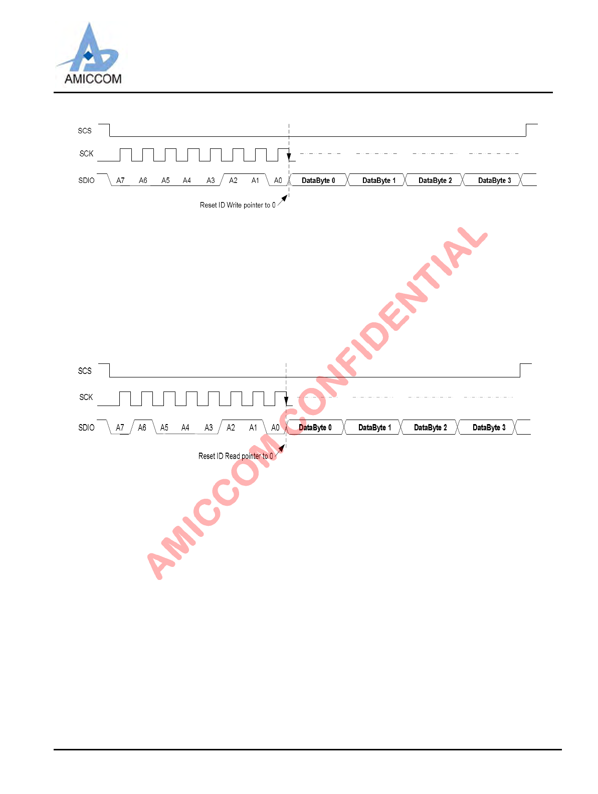
LBA7130
Oct., 2012, Version 0.6 (PRELIMINARY) 47 AMICCOM Electronics Corporation
Figure 10.15 ID Write Command Timing Chart
10.6.2 ID Read Command
User can refer to Figure 10.2 for SPI read timing chart in details. Below is the procedure of ID read command.
Step1: Deliver A7~A0 = 01000110 (A6=1 for read, A5~A0 = 000110 for ID addr, 06h).
Step2: SDIO pin outputs 32-bits ID in sequence by Data Byte 0, 1, 2 and 3.
Step3: Toggle SCS pin to high when step2 is completed.
Figure 10.16 ID Read Command Timing Chart
10.7 FIFO Accessing Command
To use A7130’s FIFO mode, enable FMS (01h) =1 via SPI interface. Before TX delivery, just write wanted data into TX FIFO
(05h) then issue TX Strobe command. Similarly, user can read RX FIFO (05h) once payload data is received.
MCU can use polling or interrupt scheme to do FIFO accessing. FIFO status can output to GIO1 (or GIO2) pin by setting
GIO1S (0Bh) or GIO2S (0Ch).
Figure 10.15 and 10.16 are timing charts of FIFO accessing via 3-wire SPI.
10.7.1 TX FIFO Write Command
User can refer to Figure 10.2 for SPI write timing chart in details. Below is the procedure of TX FIFO write command.
Step1: Deliver A7~A0 = 00000101 (A6=0 for write control register and issue FIFO A [5:0] = 05h).
Step2: By SDIO pin, deliver (n+1) bytes TX data into TX FIFO in sequence by Data Byte 0, 1, 2 to n.
Step3: Toggle SCS pin to high when step2 is completed.
Step4: Send Strobe command of TX mode (Figure 10.9) to do TX delivery.
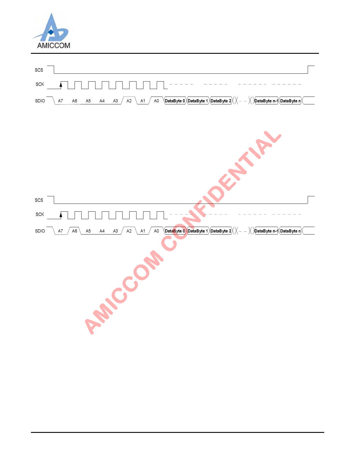
LBA7130
Oct., 2012, Version 0.6 (PRELIMINARY) 48 AMICCOM Electronics Corporation
Figure 10.17 TX FIFO Write Command Timing Chart
10.7.2 Rx FIFO Read Command
User can refer to Figure 10.2 for SPI read timing chart in details. Below is the procedure of RX FIFO read command.
Step1: Deliver A7~A0 = 01000101 (A6=1 for read control register and issue FIFO at address 05h).
Step2: SDIO pin outputs RX data from RX FIFO in sequence by Data Byte 0, 1, 2 to n.
Step3: Toggle SCS pin to high when RX FIFO is read completely.
Figure 10.18 RX FIFO Read Command Timing Chart
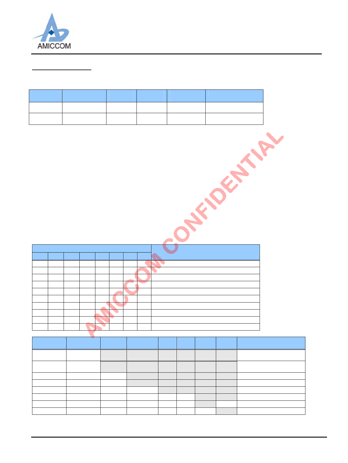
LBA7130
Oct., 2012, Version 0.6 (PRELIMINARY) 49 AMICCOM Electronics Corporation
11. State machine
From accessing data point of view, if FMS=1, FIFO mode is enabled, otherwise, A7130 is in direct mode.
SPI
chip select
SPI
Clock
SPI
Data In
SPI
Data Out
FMS register
3-Wire SPI SCS SCK SDIO SDIO FIFO (FMS=1)
Direct (FMS=0)
4-Wire SPI SCS SCK SDIO GIO1 or GIO2 FIFO (FMS=1)
Direct (FMS=0)
From current consumption point of view, A7130 has below 8 operation modes.
(1) Deep Sleep mode
(2) Sleep mode
(3) Idle mode
(4) Standby mode
(5) PLL mode
(6) TX mode
(7) RX mode
(8) Star-networking mode
11.1 Key states
After power on reset or software r eset or deep sleep m ode, user has to do c alibration pr ocess because al l control registers
are in initial values. The calibration process of A7130 is very easy, user only needs to issue Strobe commands and enable
calibration registers. And then, the calibrations are automatically completed by A7130’s internal state machine. Table 11.1
shows a summary of key circuitry among those strobe commands.
Strobe Command when AFIDS =0 (3Eh) and MIDS =0 (3Eh)
Strobe Command
A7 A6 A5 A4 A3 A2 A1 A0 Description
1 0 0 0 1 0 0 0 Deep Sleep mode (I/Os are in tri-state)
1 0 0 0 1 0 1 1 Deep Sleep mode (I/Os are pulled high)
1 0 0 0 x x x x Sleep mode
1 0 0 1 x x x x Idle mode
1 0 1 0 x x x x Standby mode
1 0 1 1 x x x x PLL mode
1 1 0 0 x x x x RX mode
1 1 0 1 x x x x TX mode
1 1 1 0 x x x x FIFO write pointer reset
1 1 1 1 x x x x FIFO read pointer reset
Mode Register
retention Regulator Xtal Osc. VCO PLL RX TX Strobe Command
Deep Sleep
(Tri-state) No OFF OFF OFF OFF OFF OFF (1000-1000)b
Deep Sleep
(pull-high) No OFF OFF OFF OFF OFF OFF (1000-1011)b
Sleep Yes ON OFF OFF OFF OFF OFF (1000-xxxx)b
Idle Yes ON OFF OFF OFF OFF OFF (1001-xxxx)b
Standby Yes ON ON OFF OFF OFF OFF (1010-xxxx)b
PLL Yes ON ON ON ON OFF OFF (1011-xxxx)b
TX Yes ON ON ON ON OFF ON (1101-xxxx)b
RX Yes ON ON ON ON ON OFF (1100-xxxx)b
Remark: x means “don’t care”
Table 11.1. Operation mode and strobe command
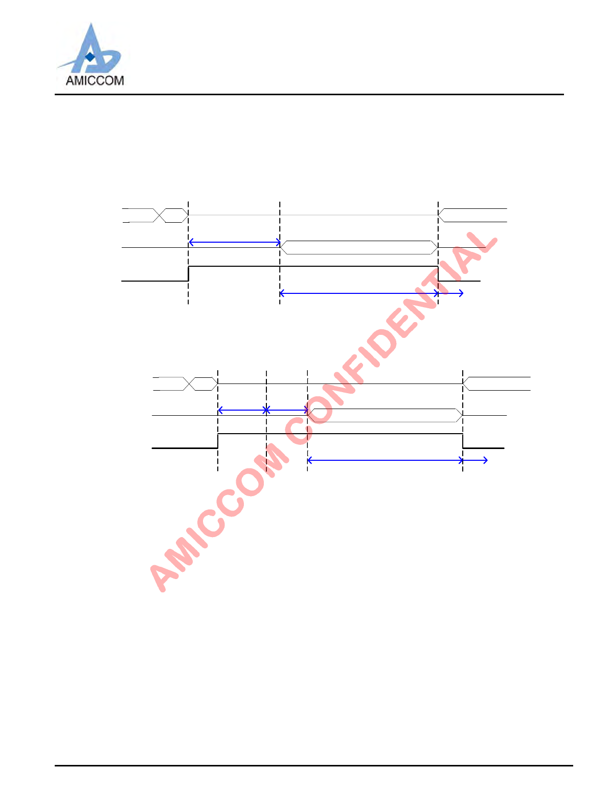
LBA7130
Oct., 2012, Version 0.6 (PRELIMINARY) 50 AMICCOM Electronics Corporation
11.2 FIFO mode
This mode is suitable for the requirements of general purpose applications and can be chosen by setting FMS = 1. After
calibration, user can issue Strobe command to enter standby mode where write TX FIFO or read RX FIFO. From standby
mode to packet data transmission, only one Strobe command is needed. Once transmission is done, A7130 is auto back to
standby mode. Figure 11.1 and Figure 11.2 are TX and RX timing diagram respectively. Figure 11.3 illustrates state diagram
of FIFO mode.
Strobe CMD
(SCS,SCK,SDIO)
T0 T2
T1
TX
Strobe
GIO1 Pin - WTR
(GIO1S[3:0]=0000)
RF settling
10us +(PDL+TDL)
Next Instruction
Preamble + ID Code + Payload
RFO Pin
Transmitting Time
Auto Back
Standby Mode
Figure 11.1 TX timing of FIFO Mode
Strobe CMD
(SCS,SCK,SDIO)
T0 T3
T2
RX
strobe
GIO1 Pin - WTR
(GIO1S[3:0]=0000)
RX settling
Next Instruction
Preamble + ID Code + Payload
RFI Pin
Receiving Time
Auto Back
Standby Mode
T1
Wait
Packet
Figure 11.2 RX timing of FIFO Mode
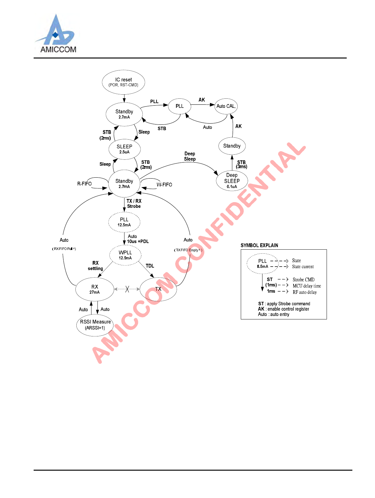
LBA7130
Oct., 2012, Version 0.6 (PRELIMINARY) 51 AMICCOM Electronics Corporation
Figure 11.3 State diagram of FIFO Mode
11.3 Direct mode
This mode is suitable to let MCU to drive customized packet to A7130 directly by setting FMS = 0. In TX mode, MCU shall
send customized packet in bit sequence (simply called raw TXD) to GIO1 or GIO2 pin. In RX mode, the receiving raw bit
streams (simply called RXD) can be configured output to GIO1 or GIO2 pin. Be aware that a customized packet shall be
preceded by a 32 bits preamble to let A7130 get a suitable DC estimation voltage. After calibration flow, for every state
transition, user has to issue Strobe command to A7130 for fully manual control. This mode is also suitable for the requirement
of versatile packet format.
Figure 11.4 and Figure 11.5 are TX and RX timing diagram in direct mode respectively. Figure 14.6 illustrates state diagram
of direct mode.
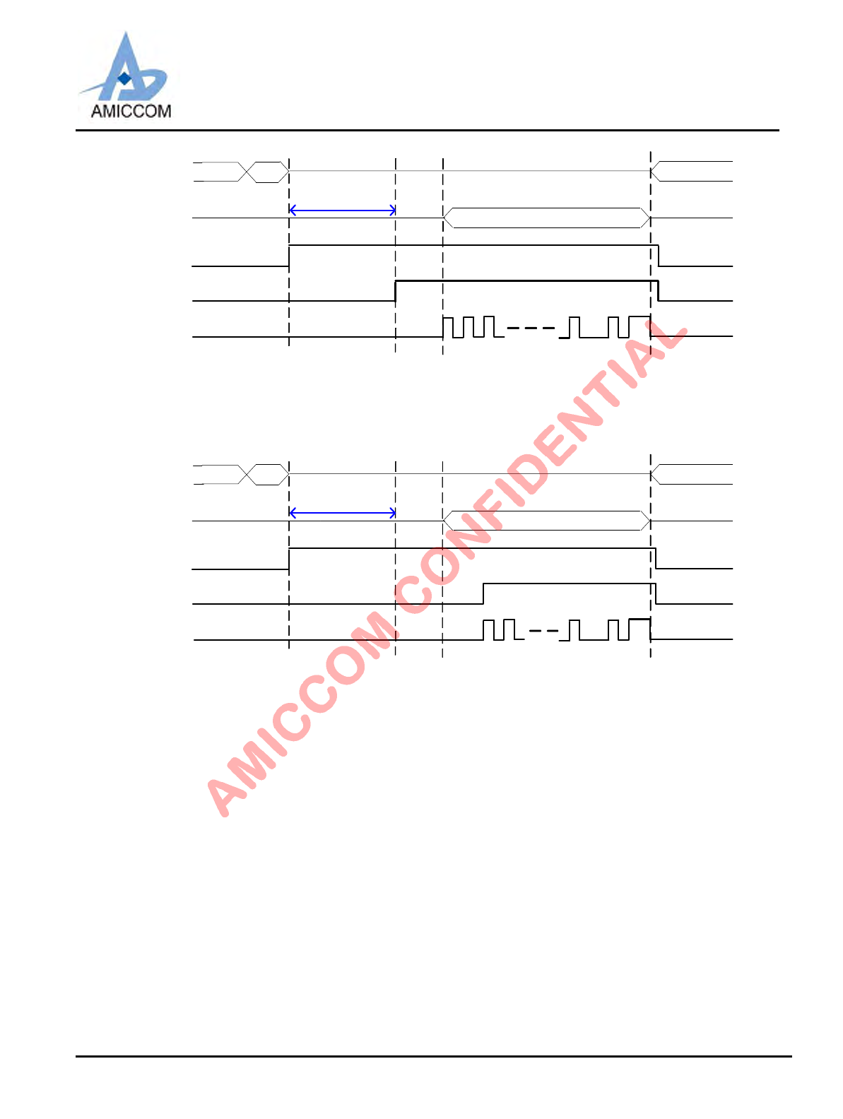
LBA7130
Oct., 2012, Version 0.6 (PRELIMINARY) 52 AMICCOM Electronics Corporation
Strobe CMD
(SCS,SCK,SDIO)
T0 T4T1
TX
Strobe
GIO1 Pin - WTR
(GIO1S[3:0]=0000)
RF settling
10us+(PDL+TDL)
STB strobe
Preamble + customized raw TXD
RFO Pin
Manually back
to STB
GIO1 Pin - TMEO
(GIO1S[3:0]=0010)
GIO2 Pin - TXD
(GIO2S[3:0]=1001)
Carrier
only
Modulated signals
32-bits
preamble
Modulation auto enable
T3
Figure 11.4 TX timing of Direct Mode
Strobe CMD
(SCS,SCK,SDIO)
T0 T4T1
RX
Strobe
GIO1 Pin - WTR
(GIO1S[3:0]=0000)
RX settling
STB strobe
Preamble + customized raw TXD
RFO Pin
Manually back
to STB
GIO1 Pin - PMDO
(GIO1S[3:0]=0011)
GIO2 Pin - RXD
(GIO2S[3:0]=1000)
Wait
packet Coming packet
Preamble detect output
T3
Figure 11.5 RX timing of Direct Mode
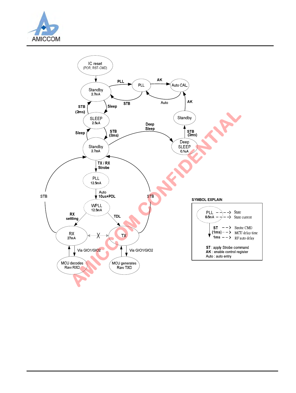
LBA7130
Oct., 2012, Version 0.6 (PRELIMINARY) 53 AMICCOM Electronics Corporation
Figure 11.6 State diagram of Direct Mode
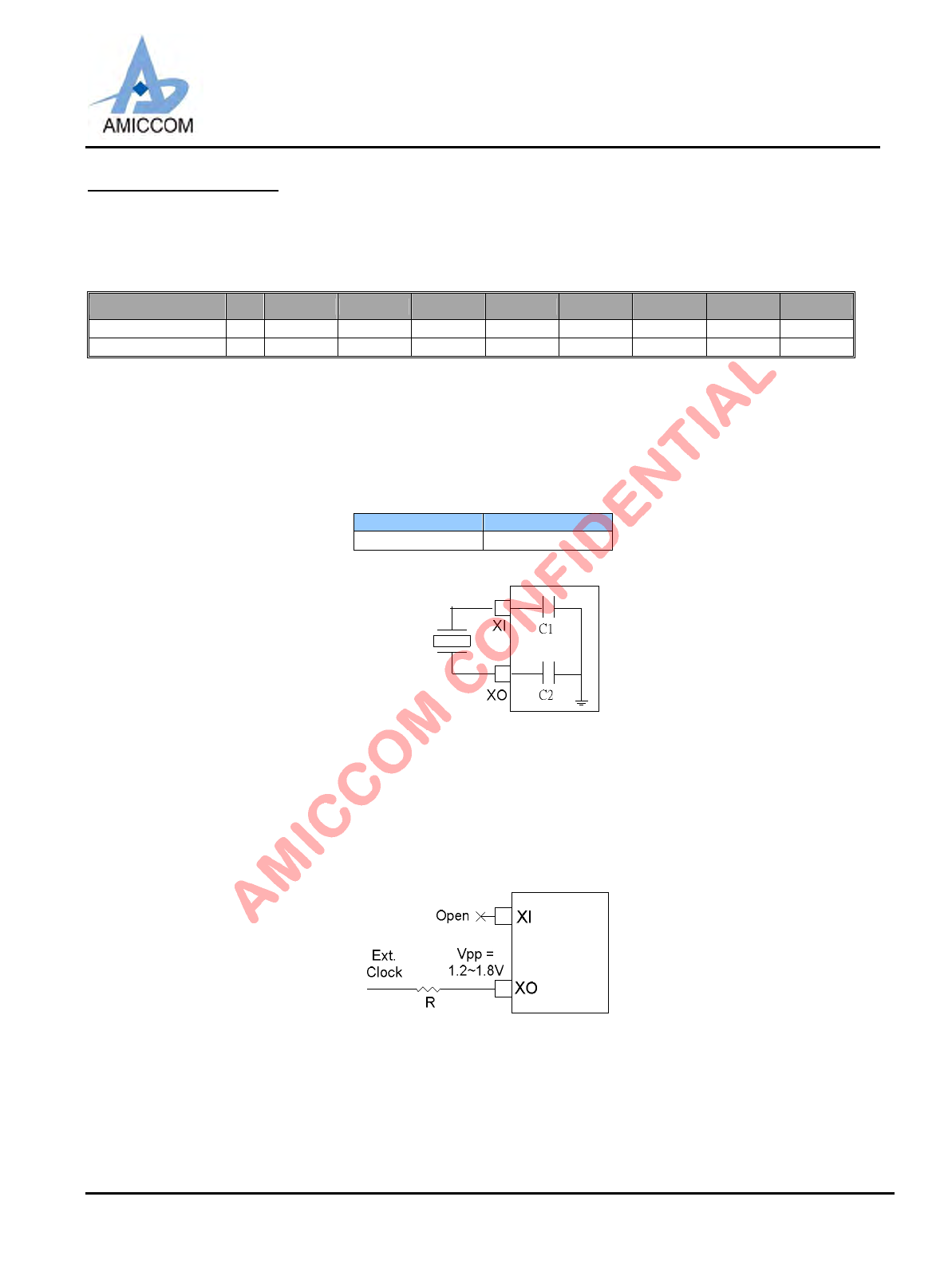
LBA7130
Oct., 2012, Version 0.6 (PRELIMINARY) 54 AMICCOM Electronics Corporation
12. Crystal Oscillator
A7130 needs external crystal or external clock that is either 16 MHz (or 18MHz) to generate internal wanted clock.
Relative Control Register
Clock Register (Address: 0Dh)
Name R/W Bit 7 Bit 6 Bit 5 Bit 4 Bit 3 Bit 2 Bit 1 Bit 0
Clock W CGC1 CGC0 GRC3 GRC2 GRC1 GRC0 CGS XS
RIFS1 IFS0 GRC3 GRC2 GRC1 GRC0 -- --
12.1 Use External Crystal
Figure 12.1 shows the connection of crystal network between XI and XO pins. C1 and C2 capacitance built inside A7130 are
used to adjust different crystal loading. User can set INTXC [4:0] to meet crystal loading requirement. A7130 supports low
cost crystal within ± 50 ppm accuracy. Be aware that crystal accuracy requirement includes initial tolerance, temperature drift,
aging and crystal loading.
Crystal Accuracy Crystal ESR
±50 ppm ≦80 ohm
Fig12.1 Crystal oscillator circuit, set INTXC[4:0] for the internal C1 and C2 values.
12.2 Use External Clock
A7130 has built-in AC couple capacitor to support external clock input. Figure 12.2 shows how to connect. In such case, XI pin
is left opened. XS shall be low to select external clock. The frequency accuracy of external clock shall be controlled within ± 50
ppm, and the amplitude of external clock shall be within 1.2 ~ 1.8 V peak-to-peak.
Fig12.2 External clock source. R is used to tune Vpp = 1.2~1.8V
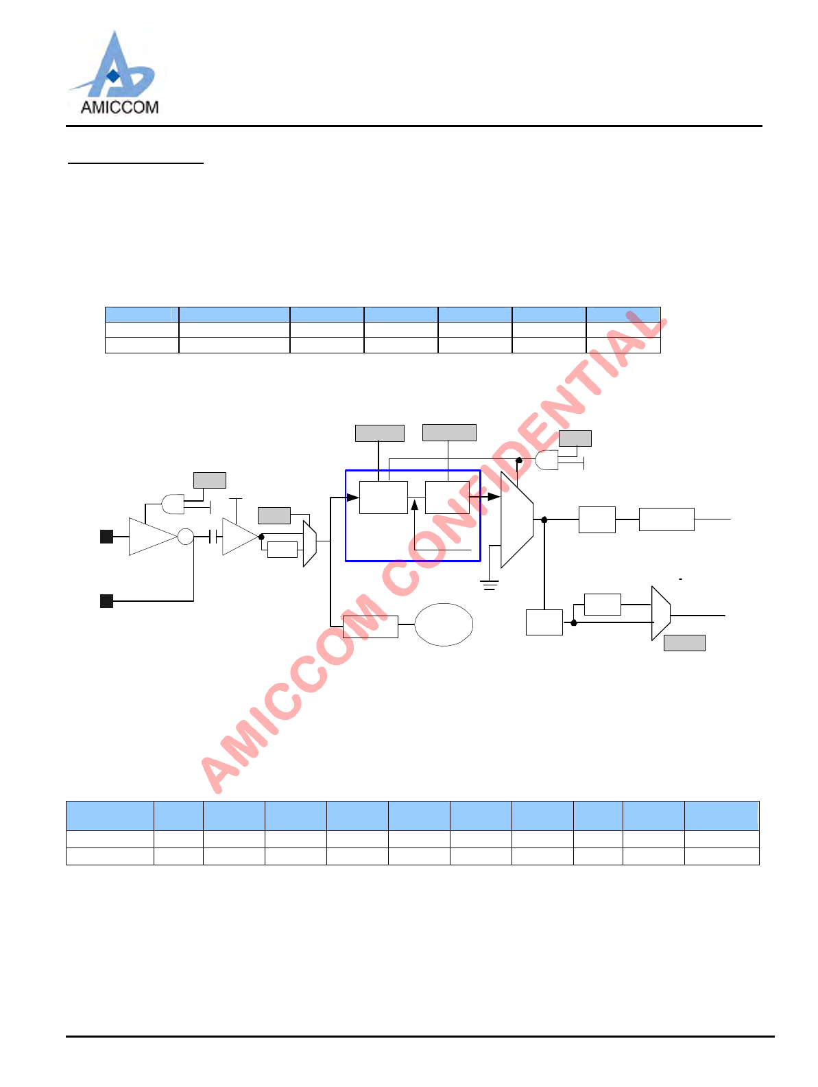
LBA7130
Oct., 2012, Version 0.6 (PRELIMINARY) 55 AMICCOM Electronics Corporation
13. System Clock
A7130 supports different crystal frequency by programmable “Clock Register”. Based on this, three important internal clocks
FCGR , FDR and FSYCK are generated.
(1) FXTAL: Crystal frequency.
(2) FXREF: Crystal Ref. Clock = FXREF * (DBL+1).
(3) FCGR: Clock Generation Reference = 2MHz = FXREF / (GRC+1).
(4) FSYCK: System Clock is related to FIF and FDR.
(6) FDR: Data Rate Clock = FIF / (SDR+1).
Data Rate DBL (0Fh) FCGR CLK Gen. FSYCK FIF FDR
4Mbps 0 (FIFO mode) 2MHz FCGR X 32 64MHz 4MHz 4MHz
4Mbps 1 (Direct mode) 2MHz FCGR X 64 128MHz 4MHz 4MHz
Table 13.1 System clock and related clock sources
XS
CE
÷
(GRC+1)
PLL
x64/x32
CGS
CE
1
0
GRC
XI
XO
X 2
DBL
CE
0
1
Clock Generator
FXREF
8MHz
/ 2
1
0
FSARS
FXTAL
FSYCK
FCGR= 2MHz
FADC
4MHz
auto
scaler / (SDR+1)
FDR
FIF
/ (RRC+1) VCO
FPFD
RDU/CGC
auto
scaler
Fig13.1 System clock block diagram
13.2 Data Rate Setting
User has to choose 16MHz Xtal (or 18MHz) for 4Mbps applications. For more data rate options, please contact AMICCOM
FAE team.
Data rate 4Mbps
Xtal DBL
(0Fh)
GRC
(0Dh)
RDU
(1Ch)
CGS
(0Dh)
RRC
(0Fh)
CGC
(0Dh)
CGS
(0Dh)
IFS
(1Ch)
SDR [7:0]
(39h) Note
16MHz 0 0111 0 1 00 10 1 11 0x00 FIFO mode
16MHz 1 1111 0 1 00 10 1 11 0x00 Direct mode
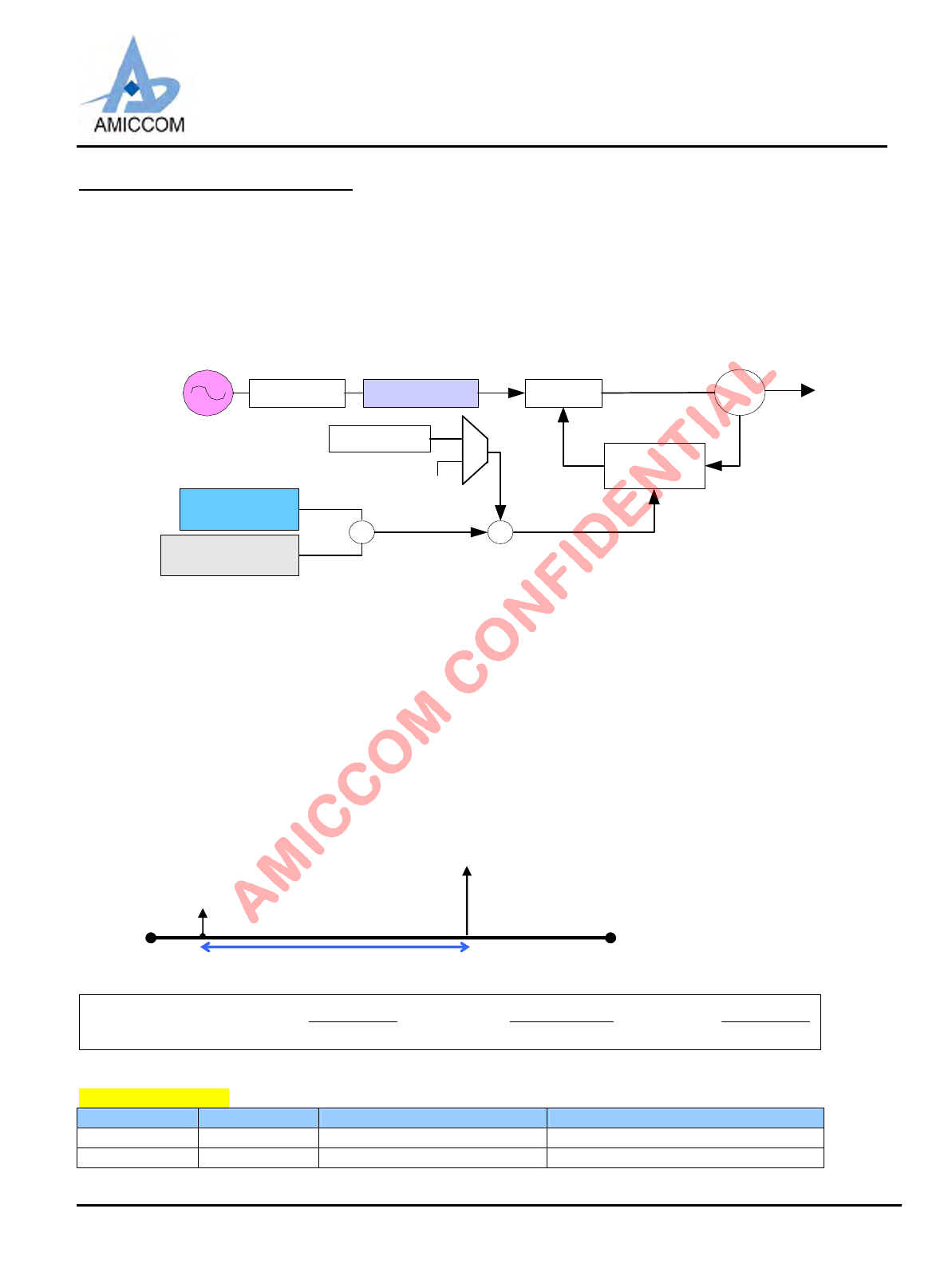
LBA7130
Oct., 2012, Version 0.6 (PRELIMINARY) 56 AMICCOM Electronics Corporation
14. Transceiver LO Frequency
A7130 is a half-duplex transceiver with embedded PA and LNA. For TX or RX frequency setting, user just needs to set up LO
(Local Oscillator) frequency for two ways radio transmission.
To target full range of 2.4GHz ISM band (2408 MHz to 2468 MHz), A7130 applies offset concept by LO frequency FLO =
FLO_BASE + FOFFSET. Therefore, this device is easy to implement frequency hopping and multi-channels by just ONE register
setting, PLL Register I (CHN [7:0]).
Below is the LO frequency block diagram.
/ (RRC[1:0]+1)X (DBL+1) PFD VCO
+
Divider
FXTAL
CHN / [4*(CHR+1)]
AC[14:0]/ 216
0
1
0
AFC
FPFD FLO
FLO
BIP[8:0] +
BFP[15:0]/ 216
+
FLO_BASE
FOFFSET
Fig14.1 Frequency synthesizer block diagram
14.1 LO Frequency Setting
From Figure 14.1, FLO is not only for TX radio frequency but also to be RX LO frequency. To set up FLO, it is easy by below 4
steps.
1. Set FLO_BASE ~ 2400.001MHz.
2. Set FCHSP = 500 KHz.
3. Set FOFFSET = CHN [7:0] x FCHSP
4. The LO frequency, FLO = FLO_BASE + FOFFSET
FLO_BASE
)
2
]0:15[
]0:8[(
1]0:1[
)1()
2
]0:15[
]0:8[( 1616
PFDLO_BASE
BFP
BIP
RRC
F
DBL
BFP
BIPFF XTAL +×
+
×+=+×=
Base on the above formula, i.e. 16 MHz, please refer to Table 14.1 and 14.2 as a calculation example to get LO frequency.
DBL = 0 for FIFO mode
STEP ITEMS VALUE NOTE
1 FXTAL 16 MHz Crystal Frequency
2DBL 0 Disable double function
F
OFFSET
F
LO_BASE
F
LO
LBA7130
Oct., 2012, Version 0.6 (PRELIMINARY) 57 AMICCOM Electronics Corporation
3RRC 0 If so, FPFD= 16MHz
4BIP[8:0] 0x096 To get FLO_BASE =2400 MHz
5 BFP[15:0] 0x0004 To get FLO_BASE ~ 2400.001 MHz
6 FLO_BASE 2400.001 MHz LO Base frequency
DBL = 1 for Direct mode
STEP ITEMS VALUE NOTE
1 FXTAL 16 MHz Crystal Frequency
2DBL 1 Enable double function
3RRC 0 If so, FPFD= 16MHz
4BIP[8:0] 0x04B To get FLO_BASE =2400 MHz
5 BFP[15:0] 0x0002 To get FLO_BASE ~ 2400.001 MHz
6 FLO_BASE 2400.001 MHz LO Base frequency
Table 14.1 How to set FLO_BASE
How to set FTXRF = FLO = FLO_BASE + FOFFSET ~ 2405.001 MHz
STEP ITEMS VALUE NOTE
1 FLO_BASE 2400.001 MHz After set up BIP and BFP
[0111] To get FCHSP= 500 KHz if DBL =0 for FIFO mode.2 CHR[3:0]
[1111] To get FCHSP= 500 KHz if DBL =1 for Direct mode.
4CHN[7:0] 0x0A FOFFSET= 500 KHz * (CHN) = 5MHz
6 FLO 2405.001 MHz Get FLO= FLO_BASE + FOFFSET
7 FTXRF 2405.001 MHz FTXRF = FLO
Table 14.2 How to set FTXRF
For 16MHz crystal, below is the calculation detail for FFPD and FCHSP.
[]
( )
10:34 +×
=
CHR
F
FPFD
CHSP
FXTAL (M Hz) DBL
(0Fh)
RRC
(0Fh) FPFD (MHz) CHR [3:0] FCHSP (KHz) Note
16 0 00 16 0111 500 Recommend
16 1 00 32 1111 500 Recommend
14.2 IF Side Band Select
Since A7130 is a low-IF TRX, in RX mode, the FRXLO shall be set to shift a FIF (i.e. FIF = 4MHz @ 4Mbps) regarding to coming
FTXRF. Therefore, A7130 offers two methods to set up FLO while A7130 is exchanging from TX mode to RX mode.
AIF register is used to enable Auto IF function for Auto IF exchange mode. And ULS registers is used for fast exchange mode
because of reduction of PLL settling time.
(1) Auto IF exchange mode
AIF (01h) ULS (19h) FRXLO Formula Note
1 0 FRXLO = FLO - F
IF Auto-minus a FIF because ULS = 0
1 1 FRXLO = FLO + F
IF Auto-plus a FIF because ULS = 1
(2) Fast exchange mode
AIF (01h) ULS (19h) FRXLO Formula Note
0 0 FRXLO = FLO The coming FTXRF shall be (FRXLO + FIF )
0 1 FRXLO = FLO The coming FTXRF shall be (FRXLO - FIF )
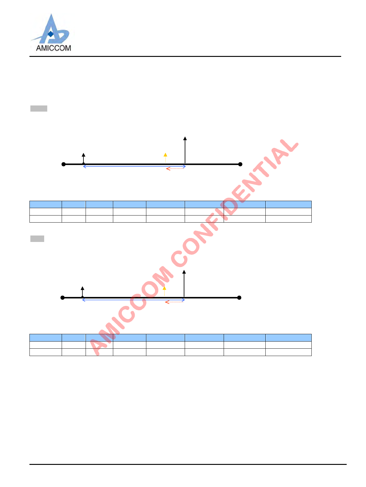
LBA7130
Oct., 2012, Version 0.6 (PRELIMINARY) 58 AMICCOM Electronics Corporation
14.2.1 Auto IF Exchange
A7130 supports Auto IF offset function by setting AIF = 1. In such case, FTXRF between master and slave is the same so that
there is only one carrier frequency (Fcarrier) during communications. Meanwhile, FRXLO during TRX exchanging is auto shifted
FIF. See below Figures and Table 14.3 for details.
Master
AIF=1 and ULS=0, FRXLO is auto shifted lower than FTXRF for a (FIF).
Master AIF ULS CHN[7:0] FCHSP (KHz) FLO_BASE (MHz) FTXRF (MHz) FRXLO (MHz)
TX 1 0 0x0A 500 2400.001 2405.001 --
RX 1 0 0x0A 500 2400.001 -- 2401.001
Slave
AIF=1 and ULS=0, FRXLO is auto shifted lower than FTXRF for a (FIF).
Slave AIF ULS CHN[7:0] FCHSP (KHz) FLO_BASE (MHz) FTXRF (MHz) FRXLO (MHz)
TX 1 0 0x0A 500 2400.001 2405.001 --
RX 1 0 0x0A 500 2400.001 -- 2401.001
Table 14.3 Auto IF exchange mode while TRX exchanging
FOFFSET =5MHz
F
IF
4MHz @ 4Mbps
F
RXLO
F
LO_BASE
F
TXRF
= F
LO
=
F
Carrier
FOFFSET =5MHz
F
RXLO
F
LO_BASE
F
TXRF
= F
LO
=
F
Carrier
F
IF
4MHz @ 4Mbps
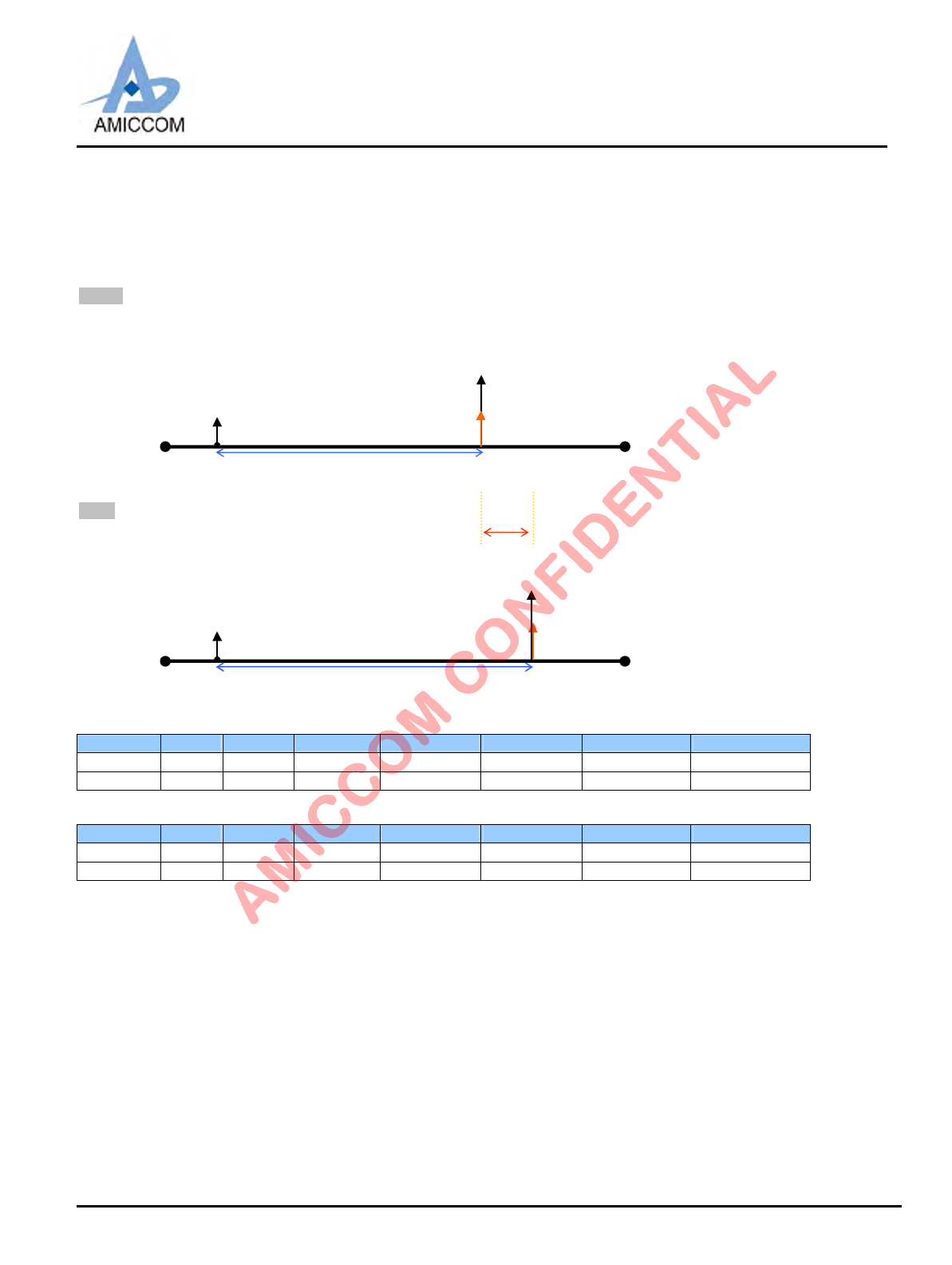
LBA7130
Oct., 2012, Version 0.6 (PRELIMINARY) 59 AMICCOM Electronics Corporation
14.2.2 Fast Exchange
Fast exchange can reduce the PLL settling time during TRX exchanging because FRXLO and FTXRF are kept to the same FLO in
either master or slave side. However, there are two on-air frequency (FCarrier (master), FCarrier (slave)) during communications. In such
case, user has to control ULS =0 in master side and ULS = 1 in slave side for two ways radio. See below Figures and Table 14.4
for details.
Master
AIF=0 and ULS=0, Master is set to up side band.
Slave
AIF=0 and ULS=1, Slave is set to low side band.
Master AIF ULS CHN[7:0] FCHSP (KHz) FLO_BASE (MHz) FTXRF (MHz) FRXLO (MHz)
TX 0 0 0x0A 500 2400.001 2405.001 --
RX 0 0 0x0A 500 2400.001 -- 2405.001
Slave AIF ULS CHN[7:0] FCHSP (KHz) FLO_BASE (MHz) FTXRF (MHz) FRXLO (MHz)
TX 0 1 0x12 500 2400.001 2409.001 --
RX 0 1 0x12 500 2400.001 -- 2409.001
Table 14.4 Fast exchange mode while TRX exchanging
F
IF
4MHz @ 4Mbps
F
RXLO
FOFFSET =9MHz
F
LO_BASE
FRXLO
F
LO_BASE
F
TXLO
=
F
LO
=
F
Carrier (Master)
FOFFSET =5MHz
F
TXLO
=
F
LO
=
F
Carrier (Slave)
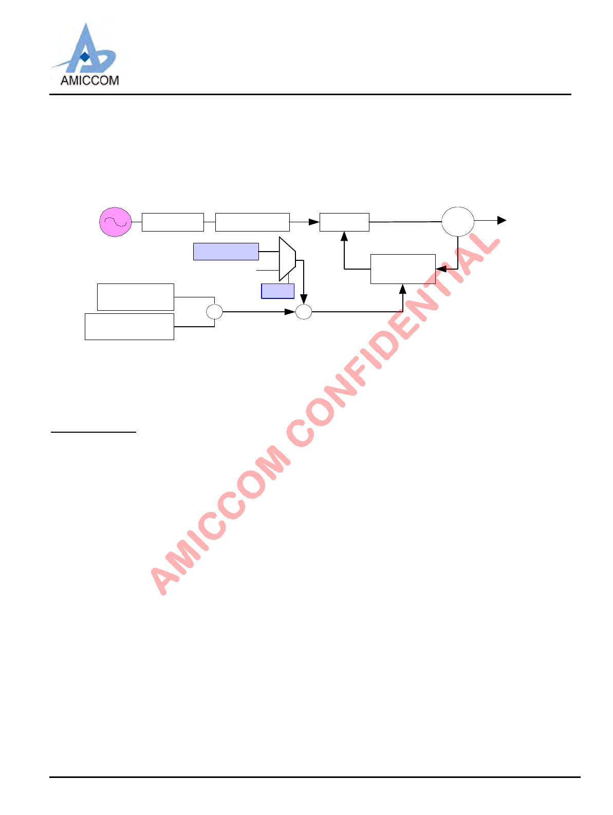
LBA7130
Oct., 2012, Version 0.6 (PRELIMINARY) 60 AMICCOM Electronics Corporation
14.3 Auto Frequency Compensation
The AFC function (Auto Frequency Compensation) supports to use low accuracy crystal (±50 ppm) on A7130 without sensitivity
degradation. The AFC concept is automatically fine tune RX LO frequency (FRXLO). User can read AC [14:0] to know the
compensation value of FRXLO.
/ (RRC[1:0]+1)X (DBL+1) PFD VCO
+
Divider
FXTAL
CHN / [4*(CHR+1)]
AC[14:0]/ 216
0
1
0
AFC
FPFD FLO
FLO
BIP[8:0] +
BFP[15:0]/ 216
+
FLO_BASE
FOFFSET
Figure 14.3 Block Diagram of enabling AFC function
For AFC procedure, please refer to A7130’s reference code and contact AMICCOM FAE team for details.
15. Calibration
A7130 needs calibration process after deep sleep mode or power on reset or software reset. Below are six calibration items
inside the device.
1. VCO Current Calibration.
2. VCO Bank Calibration.
3. VCO Deviation Calibration.
4. IF Filter Bank Calibration.
5. RSSI Calibration.
6. RC Oscillator Calibration.
15.1 Calibration Procedure
The purpose to execute the above calibration items is to deal with Foundry process deviation. After calibrations, A7130 will be
set to the best working conditions without concerning Foundry process deviation to impact A7130’s RF performance.
In general, user can use A7130’s auto calibration function by just enabling calibration items and checking its calibration flag. For
detailed calibration procedures, please refer to A7130 reference code of initRF() subroutine and A7130_Cal() subroutine.
1. Initialize A7130 by calling the subroutine of initRF().
n Initialize all control registers by calling the subroutine of A7130_Config().
n Execute all calibration items by calling the subroutine of A7130_Cal().
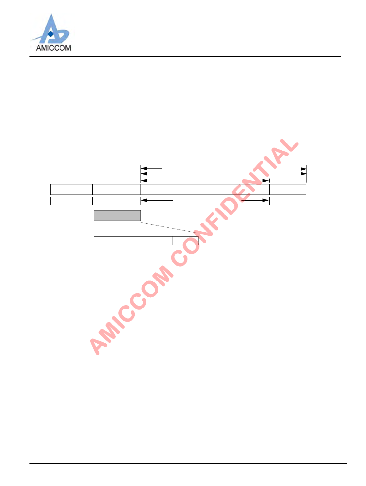
LBA7130
Oct., 2012, Version 0.6 (PRELIMINARY) 61 AMICCOM Electronics Corporation
16. FIFO (First In First Out)
A7130 has the separated physical 64-bytes TX and RX FIFO inside the device. To use A7130’s FIFO mode, user just needs to
enable FMS =1. For FIFO accessing, TX FIFO (write-only) and RX FIFO (read-only) share the same register address 05h. TX
FIFO represents transmitted payload. On the other hand, RX circuitry synchronizes ID Code and stores received payload into
RX FIFO.
16.1 TX Packet Format in FIFO mode
16.1.1 Basic FIFO mode
If FCL[1:0] = 00 and ENRL = 0, A7130 is formed a Basic FIFO mode which can also support Auto-ack/ Auto-resend function.
There is no MAC header in TX packet format. ID code is a PHY header used to be the frame sync to enable RX FIFO receiving.
ID codePreamble Payload (CRC)
4 bytes 4 bytes 2 bytesPhy. 64 bytes
CRC -16 calculation(optional)
FEC encoded/decoded(optional)
Data whitening(optional)
Figure 16.1 TX packet format of basic FIFO mode
Preamble:
The packet is led by a self-generated preamble which is composed of alternate 0 and 1. If the first bit of ID code is 0, preamble
shall be 0101…0101. In the contrast, if the first bit of ID code is 1, preamble shall be 1010…1010.
Preamble length is recommended to set 4 bytes by PML [1:0] (20h).
ID code:
ID code is recommended to set 4 bytes by IDL[1:0] = [01] and ID Code is stored into ID Data register by sequence ID Byte 0, 1,
2 and 3. If RX circuitry check ID code is correct, payload will be written into RX FIFO. In addition, user can set ID code error
tolerance (0~ 7bit error) by setting ETH [2:0] during ID synchronization check.
Payload:
Payload length is programmable by FEP [11:0]. The physical FIFO depth is 64 bytes. A7130 also supports logical FIFO
extension up to 4K bytes.
CRC:
In FIFO mode, if CRC is enabled (CRCS=1), 2-bytes of CRC value is self-generated and attached at the footer of the packet. In
the same way, RX circuitry will check CRC value and show the result to CRC Flag.
16.1.2 Advanced FIFO mode
A7130 supports to self generated MAC header to form an advanced FIFO mode by enabling FCL[1:0], ENRL.. Therefore,
A7130 can support ACK FIFO (FCB1~FCB3) and dynamic FIFO length depending on configurations.
ID code
ID Byte 0 ID Byte 1 ID Byte 2 ID Byte 3
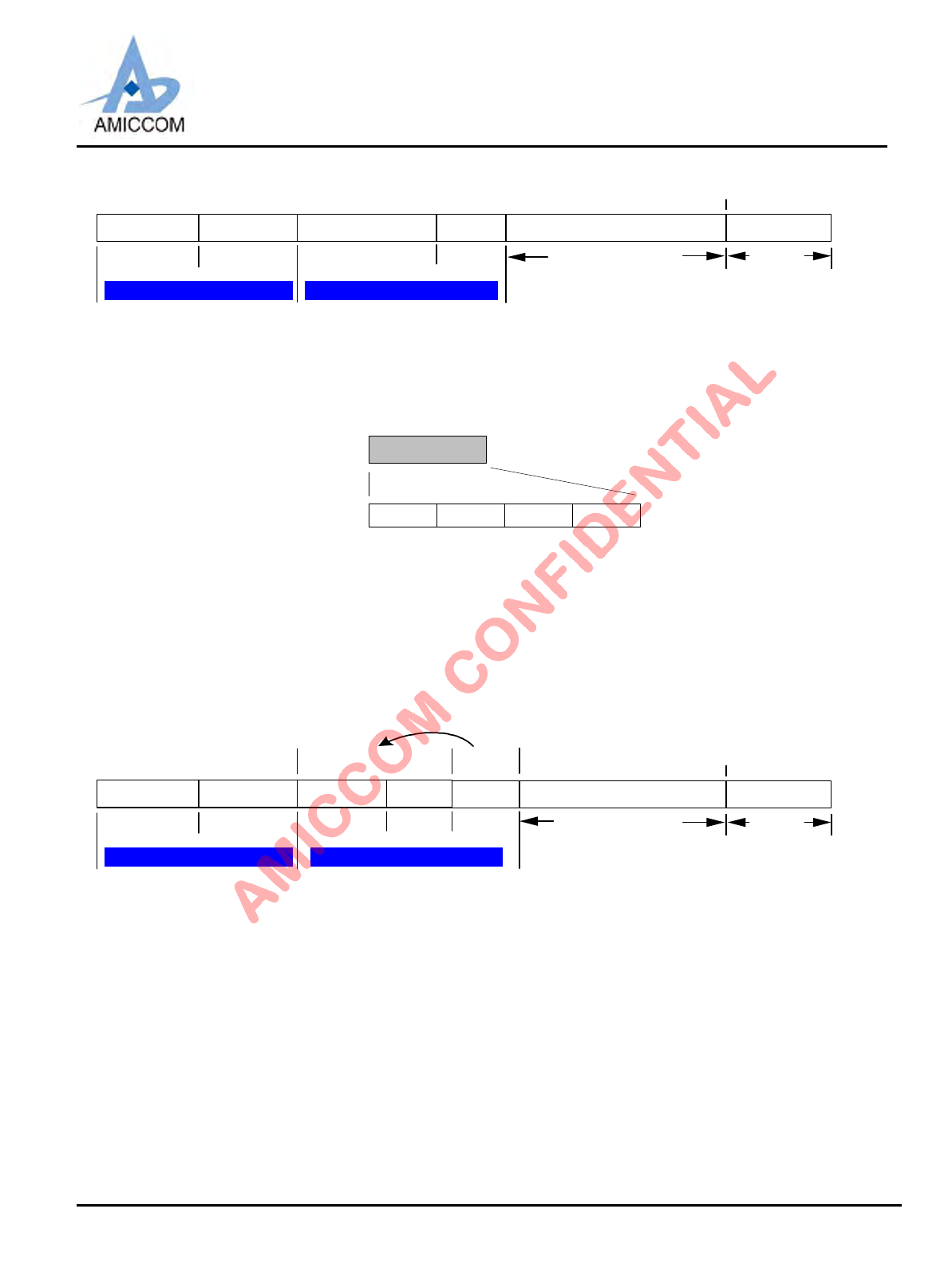
LBA7130
Oct., 2012, Version 0.6 (PRELIMINARY) 62 AMICCOM Electronics Corporation
ID codePreamble Payload (CRC)
4 bytes 4 bytes 2 bytesPhy. 64 bytes
FCB
1~4 bytes
FEP
1 2 b its
au to
ack/resend
dynamic
FIFO
M AC H eader (self-generated)PH Y H eader (self-generated)
Figure 16.2 TX packet format of advanced FIFO mode.
FCB:
If FCL[1:0] ≠00, FCB header is enabled to support ACK FIFO by (FCB1~FCB3). The FCB is frame control byte. FCB0 is NOT
allowed to program but carry a dedicated header (00111b) and SID [2:0] (Serial ID of packet number). FCB1~3 are used for
customized information in FCB field.
Figure 16.3 FCB (Frame Control Field)
FEP:
If ENRL = 1, A7130 supports dynamic FIFO. FEP [11:0] is self-generated to add into TX packet. In RX side, FEP[11:0] of the
coming TX packet will be detected and stored into LENF [11:0] register.
HEC:
If HECS = 1, A7130 supports to self-generated a HEC byte which is a local CRC-8 of the MAC header. This HEC byte is an
optional feature to calculate CRC result of MAC Header. HEC is located at the end of the MAC header.
ID codePreamble Payload (CRC)
4 bytes 4 bytes 2 bytesPhy. 64 bytes
FCB
1~4 bytes
FEP
12 b its
HEC
1 b yte
Header
CRC
M A C H eader (self-generated)PH Y H eader (self-generated)
MAC
header
Figure 16.4 HEC (CRC for MAC Header)
16.2 Bit Stream Process in FIFO mode
A7130 supports 3 optional bit stream process for payload in FIFO mode, they are,
(1) CCITT-16 CRC
(2) (7, 4) Hamming FEC
(3) Data Whitening by XOR PN7 (7-bits Pseudo Random Sequence). The initial seed of PN7 is set by WS [6:0]
CRC (Cyclic Redundancy Check):
1. CRC is enabled by CRCS= 1. TX circuitry calculates the CRC value of payload (preamble and ID code are excluded) and
transmits 2-bytes CRC value after payload.
2. RX circuitry checks CRC value and shows the result to CRCF. If CRCF=0, received payload is correct, else error
occurred.
FCB
FCB 0 FCB 1 FCB 2 FCB 3
LBA7130
Oct., 2012, Version 0.6 (PRELIMINARY) 63 AMICCOM Electronics Corporation
FEC (Forward Error Correction):
1. FEC is enabled by FECS= 1. Payload and CRC value (if CRCS=1) are encoded by (7, 4) Hamming code.
2. Each 4-bits (nibble) of payload is encoded into 7-bits code word and delivered out automatically.
(ex., 64 bytes payload will be encoded to 128 code words, each code word is 7 bits.)
3. RX circuitry decodes received code words automatically. Each code word can correct 1-bit error. Once 1-bit error
occurred, FECF=1 (00h).
Data Whitening:
1. Data whitening is enabled by WHTS= 1. Payload and CRC value (if CRCS=1) or their encoded code words (if FECS=1)
are encrypted by bit XOR operation with PN7. The initial seed of PN7 is set by WS [6:0].
2. RX circuitry decrypts received payload and 2-bytes CRC (if CRCS=1) automatically. Please noted that user shall set the
same WS [6:0] (22h) to TX and RX.
16.3 Transmission Time
Based on CRC and FEC options, the transmission time are different. See table 16.1 for details.
Data Rate = 4 Mbps
Data Rate Preamble
(bits)
ID Code
(bits)
Payload
(bits)
CRC
(bits)
FEC Transmission
Time / Packet
32 32 512 Disable Disable 576 bit X 0.25 us = 144 us
32 32 512 16 bits Disable 592 bit X 0.25 us = 148 us
32 32 512 Disable 512 x 7 / 4 960 bit X 0.25 us = 240 us
4Mbps
32 32 512 16 x 7 / 4 512 x 7 / 4 988 bit X 0.25 us = 247 us
Table 16.1 Transmission time
16.4 Usage of TX and RX FIFO
In application points of view, A7130 supports 2 options of FIFO arrangement.
(1) Easy FIFO
(2) Segment FIFO
(3) FIFO extension
For FIFO operation, A7130 supports Strobe command to reset TX and RX FIFO pointer as shown below. User can refer to
section 10.5 for details.
Strobe Command
Strobe Command
A7 A6 A5 A4 A3 A2 A1 A0 Description
1 1 1 0 x x X x FIFO write pointer reset (for TX FIFO)
1 1 1 1 x x X x FIFO read pointer reset (for RX FIFO)
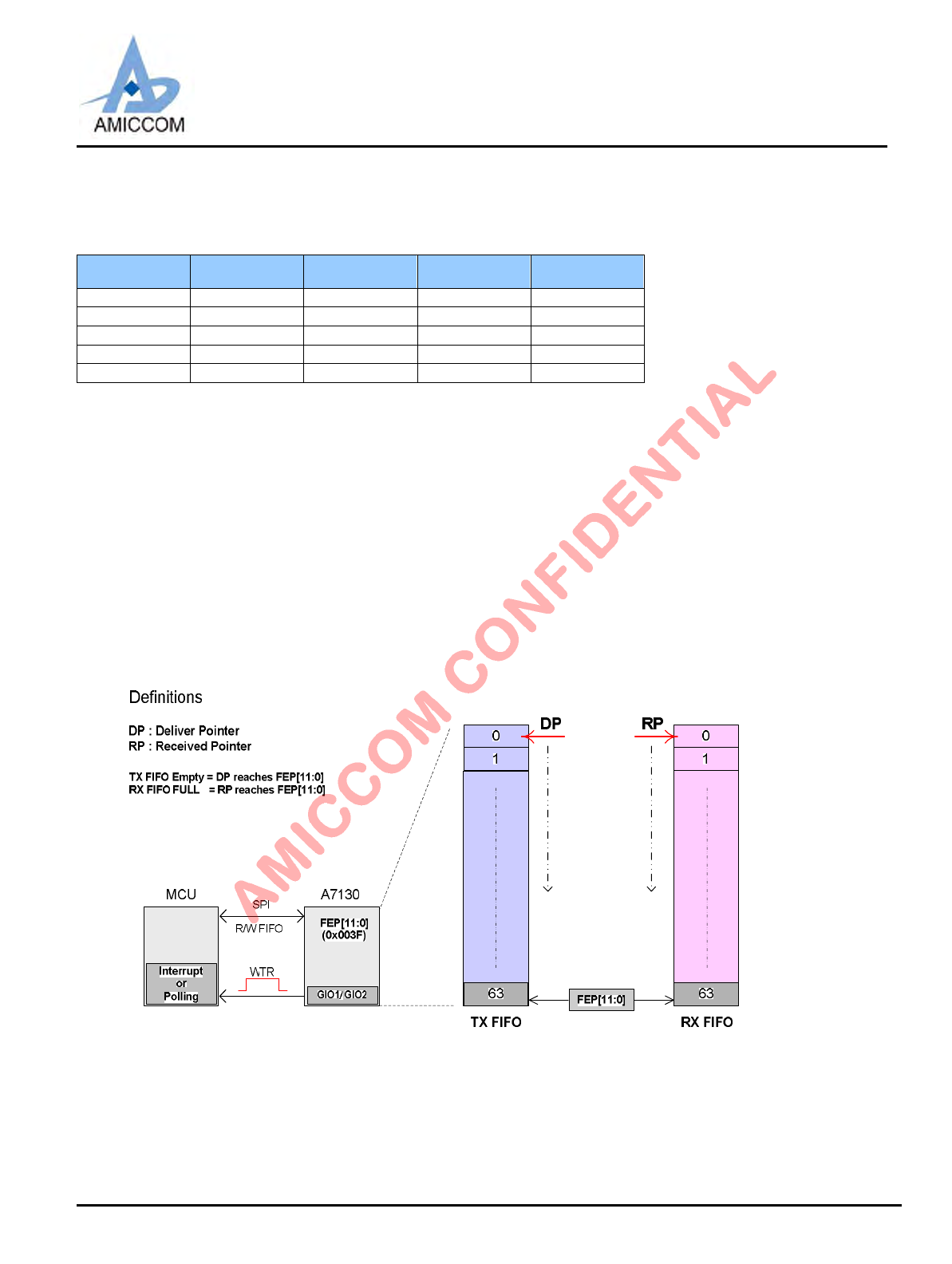
LBA7130
Oct., 2012, Version 0.6 (PRELIMINARY) 64 AMICCOM Electronics Corporation
16.4.1 Easy FIFO
In Easy FIFO mode, max FIFO length is 64 bytes. FIFO length is equal to ( FEP [11:0] +1 ) where FEP [11:0] is max 0x003F.
User just needs to control FEP [11:0] (03h) and disable PSA and FPM as shown below.
TX-FIFO
(byte)
RX-FIFO
(byte)
FEP[11:0]
(03h)
PSA[5:0]
(04h)
FPM[1:0]
(04h)
1 1 0x00 0 0
8 8 0x07 0 0
16 16 0x0F 0 0
32 32 0x1F 0 0
64 64 0x3F 0 0
Table 16.2 Control registers of Easy FIFO
Procedures of TX FIFO Transmitting
1. Initialize all control registers (refer A7130 reference code).
2. Set FEP [11:0] = 0x003F for 64-bytes FIFO.
3. Send Strobe command – TX FIFO write pointer reset.
4. MCU writes 64-bytes data to TX FIFO.
5. Send TX Strobe Command and monitor WTR signal.
6. D one.
Procedures of RX FIFO Reading
1. When RX FIFO is full, WTR (or FSYNC) can be used to trigger MCU for RX FIFO reading.
2. Send Strobe command – RX FIFO read pointer reset.
3. MCU monitors WTR signal and then read 64-bytes from RX FIFO.
4. D one.
Figure 16.5 Easy FIFO
LBA7130
Oct., 2012, Version 0.6 (PRELIMINARY) 65 AMICCOM Electronics Corporation
16.4.2 Segment FIFO
In Segment FIFO, TX FIFO length is equal to (FEP [11:0] - PSA [5:0]+1). FPM [1:0] should be zero. This function is very
useful for button applications. In such case, each button is used to transmit fixed code (data) every time. During initialization,
each fixed code is written into corresponding segment FIFO once and for all. Then, if button is triggered, MCU just assigns
corresponding segment FIFO (PSA [5:0] and FEP [11:0]) and issues TX strobe command. Table 16.4 explains the details if TX
FIFO is arranged into 8 segments, each TX segment and RX FIFO length are 8 bytes.
Segment PSA FEP TX FIFO Length PSA[5:0] FEP[11:0] FPM[1:0]
1PSA1 FEP1 8 bytes 0x00 0x07 0
2PSA2 FEP2 8 bytes 0x08 0x0F 0
3PSA3 FEP3 8 bytes 0x10 0x17 0
4PSA4 FEP4 8 bytes 0x18 0x1F 0
5PSA5 FEP5 8 bytes 0x20 0x27 0
6PSA6 FEP6 8 bytes 0x28 0x2F 0
7PSA7 FEP7 8 bytes 0x30 0x37 0
8PSA8 FEP8 8 bytes 0x38 0x3F 0
RX FIFO Length PSA[5:0] FEP[11:0] FPM[1:0]
8 bytes 0 0x0007 0
Table 16.3 Segment FIFO is arranged into 8 segments
Procedures of TX FIFO Transmitting
1. Initialize all control registers (refer A7130 reference code).
2. Issue Strobe command – TX FIFO write pointer reset.
3. MCU writes fixed code into corresponding segment FIFO once and for all.
4. To consign Segment 1, set PSA = 0x00 and FEP= 0x0007
To consign Segment 2, set PSA = 0x08 and FEP= 0x000F
To consign Segment 3, set PSA = 0x10 and FEP= 0x0017
To consign Segment 4, set PSA = 0x18 and FEP= 0x001F
To consign Segment 5, set PSA = 0x20 and FEP= 0x0027
To consign Segment 6, set PSA = 0x28 and FEP= 0x002F
To consign Segment 7, set PSA = 0x30 and FEP= 0x0037
To consign Segment 8, set PSA = 0x38 and FEP= 0x003F
5. Issue TX Strobe Command and monitor WTR signal.
6. D one.
Procedures of RX FIFO Reading
1. When RX FIFO is full, WTR (or FSYNC) is used to trigger MCU for RX FIFO reading.
2. Issue Strobe command – RX FIFO read pointer reset.
3. MCU monitors WTR signal and then read 8-bytes from RX FIFO.
4. D one.
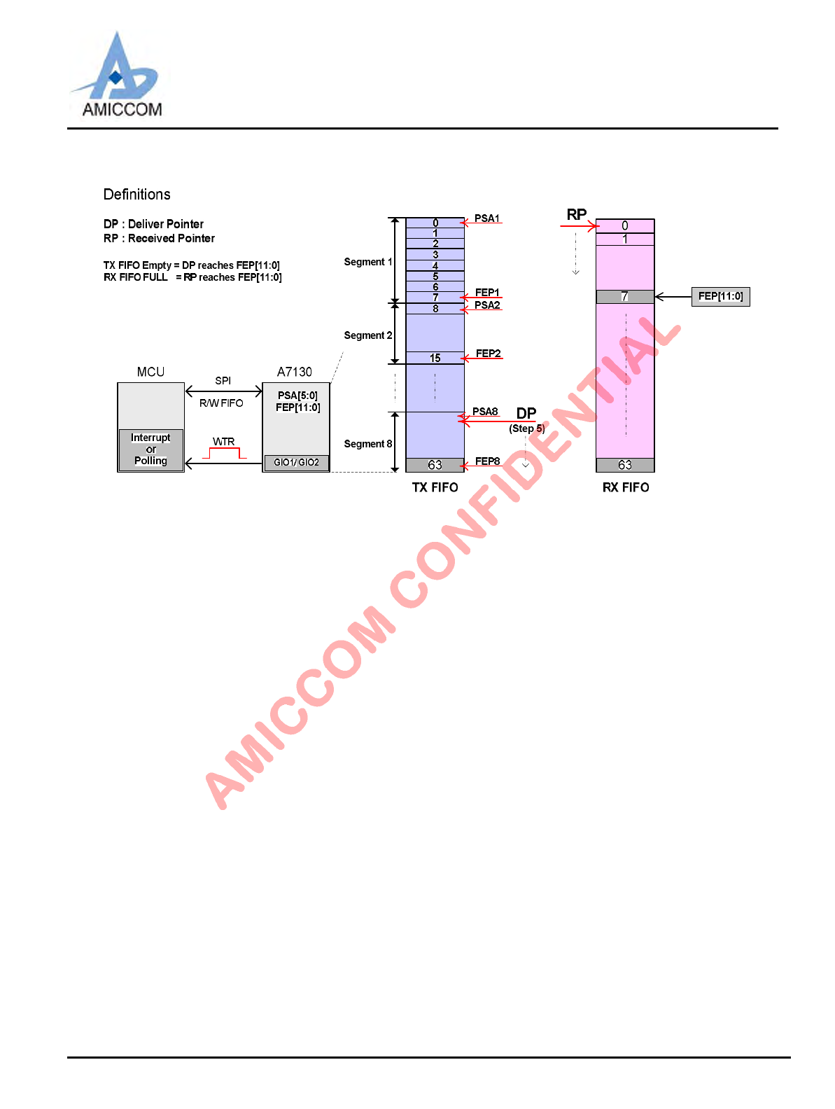
LBA7130
Oct., 2012, Version 0.6 (PRELIMINARY) 66 AMICCOM Electronics Corporation
Figure 16.6 Segment FIFO Mode
LBA7130
Oct., 2012, Version 0.6 (PRELIMINARY) 67 AMICCOM Electronics Corporation
16.4.3 FIFO Extension
A7130 supports FIFO extension up to 4K bytes from the 64 bytes physical TX FIFO and RX FIFO. The FIFO extension length is
configured by (FEP [11:0] +1 and PSA [5:0] =0). FPM [1:0] is used to set the FPF threshold which FPF is FIFO Pointer Flag to
inform MCU the timing of reading RX FIFO and refilling TX FIFO.
Please be notice, SPI speed is important to prevent error operation (over-write) in FIFO extension mode. We recommend the
min. SPI speed shall be equal or greater than (A70 on-air data rate + 500Kbps).Please refer to A7130’s reference code
(FIFO extension) for details.
For example, if A7130 data rate = 4Mbps and FIFO extension = 256 bytes.
TX RX Control Registers
FIFO
Length
(byte)
FPF
Threshold
Max. SPI
Data Rate
FIFO
Length
(byte)
FPF
Threshold
Max. SPI
Data Rate
FEP[7:0] FPM[1:0] PSA[5:0]
Delta = 04 10 Mbps Delta = 60 10 Mbps 00 0
Delta = 08 10 Mbps Delta = 56 10 Mbps 01 0
Delta = 12 10 Mbps Delta = 52 10 Mbps 10 0
256
Delta = 16 8 Mbps
256
Delta = 48 8 Mbps
0xFF
11 0
Table 16.4 How to set FIFO extension when A7130 is at 4Mbps data rate
Procedures of TX FIFO Extension
1. Initialize all control registers (refer A7130 reference code).
2. Set FEP [11:0] = 0x0FF for 256-bytes FIFO extension.
3. Set FPM [1:0] = 11 for FPF threshold.
4. Set CKO Register = 0x12
5. Issue Strobe command – TX FIFO write pointer reset.
6. MCU writes 1st 64-bytes TX FIFO.
7. Issue TX Strobe command.
8. MCU monitors FPF from A7130’s CKO pin.
9. FPF triggers MCU to write 2nd 48-bytes TX FIFO.
10. Monitor FPF.
11. FPF triggers MCU to write 3rd 48-bytes TX FIFO.
12. Monitor FPF.
13. FPF triggers MCU to write 4th 48-bytes TX FIFO.
14. Monitor FPF.
15. FPF triggers MCU to write 5th 48-bytes TX FIFO.
16. D one.
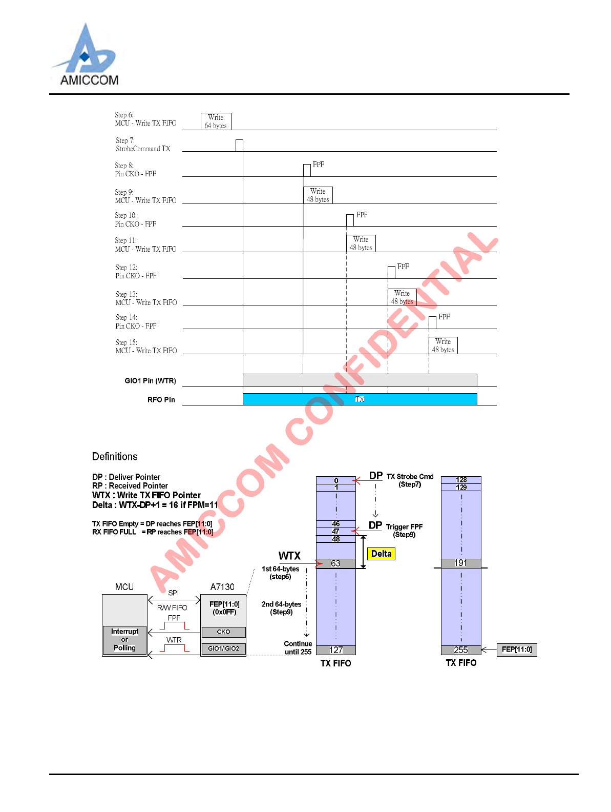
LBA7130
Oct., 2012, Version 0.6 (PRELIMINARY) 68 AMICCOM Electronics Corporation
Figure 16.7 TX FIFO Extension
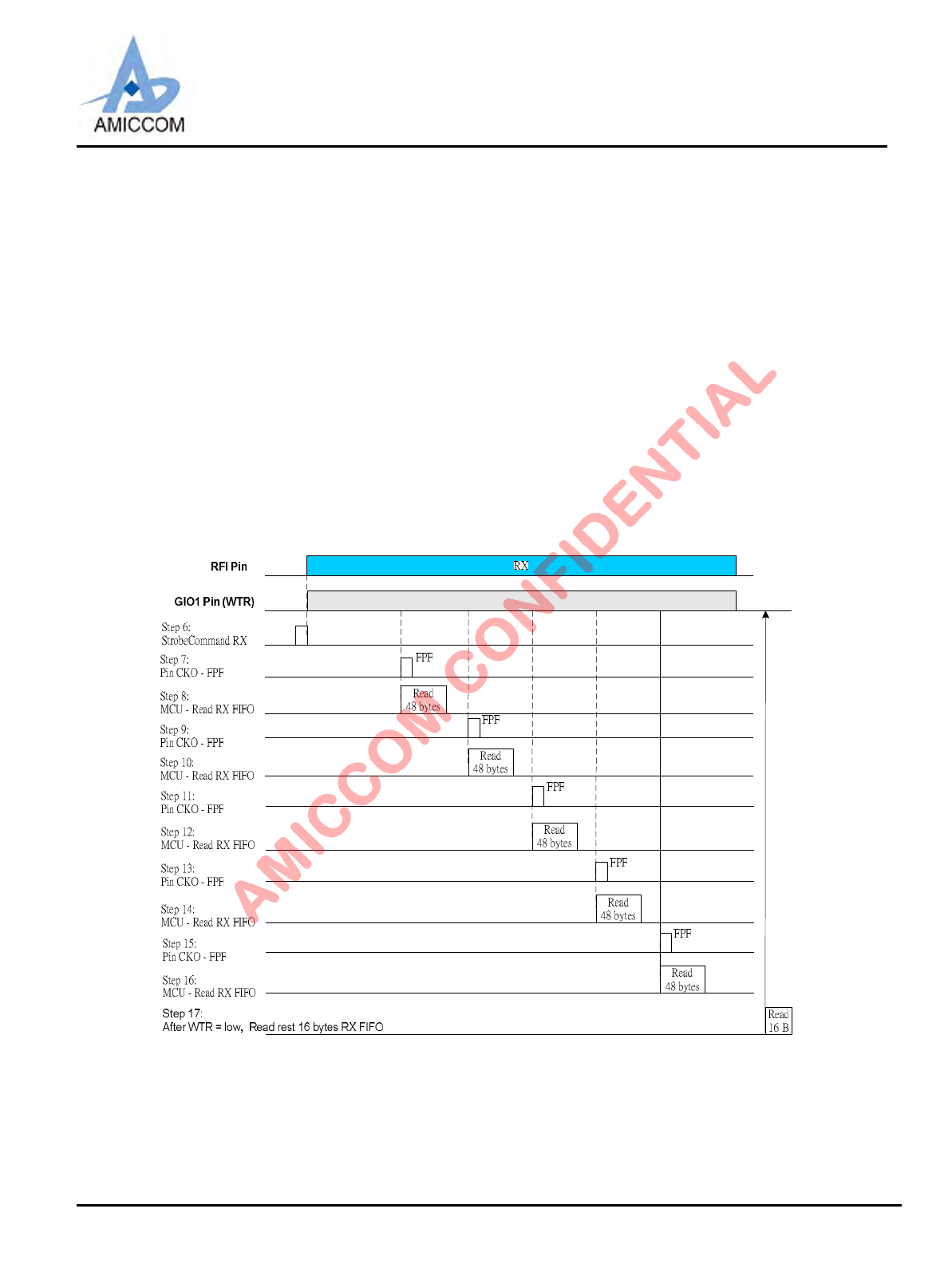
LBA7130
Oct., 2012, Version 0.6 (PRELIMINARY) 69 AMICCOM Electronics Corporation
Procedures of RX FIFO Reading
1. Initialize all control registers (refer A7130 reference code).
2. Set FEP [11:0] = 0x0FF for 256-bytes FIFO extension.
3. Set FPM [1:0] = [11b] for FPF threshold.
4. Set CKO Register = 0x12
5. Issue Strobe command – RX FIFO read pointer reset.
6. Issue RX Strobe command.
7. MCU monitors FPF from A7130’s CKO pin.
8. FPF triggers MCU to read 1st 48-bytes RX FIFO.
9. Monitor FPF.
10. FPF triggers MCU to read 2nd 48-bytes RX FIFO.
11. Monitor FPF.
12. FPF triggers MCU to read 3rd 48-bytes RX FIFO.
13. Monitor FPF.
14. FPF triggers MCU to read 4th 48-bytes RX FIFO.
15. Monitor FPF.
16. FPF triggers MCU to read 5th 48-bytes RX FIFO.
17. Monitor WTR falling edge or WTR = low, read the rest 16-bytes RX FIFO
18. D one.
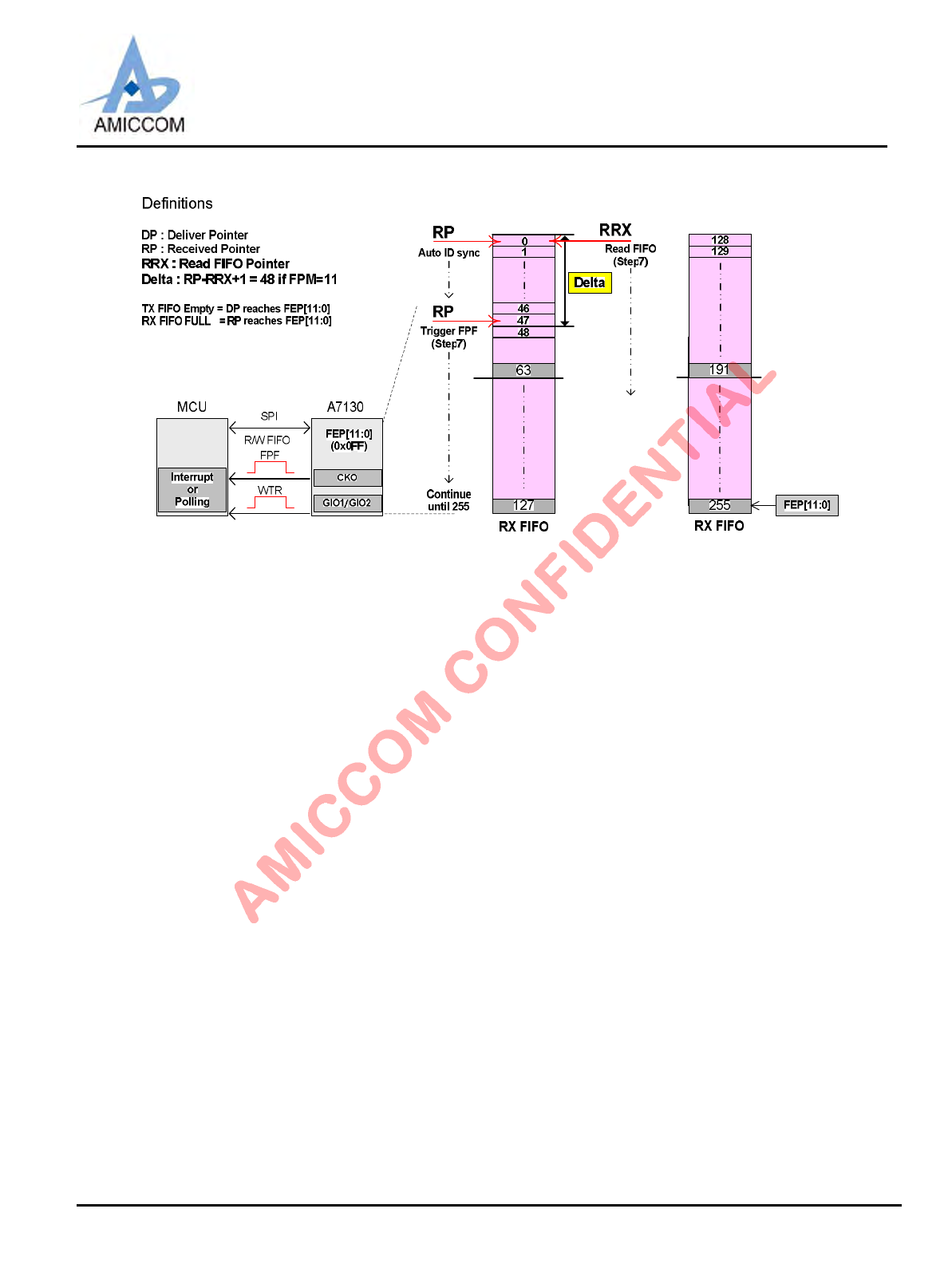
LBA7130
Oct., 2012, Version 0.6 (PRELIMINARY) 70 AMICCOM Electronics Corporation
Figure 16.8 RX FIFO Extension Mode
LBA7130
Oct., 2012, Version 0.6 (PRELIMINARY) 71 AMICCOM Electronics Corporation
17. ADC (Analog to Digital Converter)
A7130 has built-in 8-bits ADC for RSSI measurement and internal thermal sensor by enabling ADCM. User can just use the
recommended va lues of ADC from Tab le 17.1. P lease noted tha t ADC clock can be selected by s etting FSARS (4MHz or
8MHz). The ADC converting time is 20 x ADC clock periods.
XADS
(1Fh)
RSS
(1Ch)
ARSSI
(01h)
ADCM
(01h)
ERSSM
(1Ch)
FSARS
(1Fh)
CDM
(1Fh) Standby Mode RX Mode
0111101Thermal sensor RSSI
Table 17.1 Setting of RSSI measurement
17.1 RSSI Measurement
A7130 supports 8-bits digital RSSI to detect RF signal strength. RSSI value is stored in ADC [7:0] (1Eh). Fig 17.1 shows a
typical plot of RSSI reading as a function of input power. Be aware RSSI accuracy is about ± 6dBm.
ADC value Curve (AGC on,25℃)
0
50
100
150
200
250
300
-110 -105 -100 -95 -90 -85 -80 -75 -70 -65 -60 -55 -50 -45 -40 -35 -30 -25 -20 -15 -10 -5 0 5 10
Input Power (dBm)
ADC Value
Average
ADC value Curve (AGC off,25℃)
0
50
100
150
200
250
-110 -105 -100 -95 -90 -85 -80 -75 -70 -65 -60 -55 -50 -45 -40 -35 -30 -25 -20 -15 -10 -5 0 5 10
Input Power (dBm)
ADC Value
Average
Figure 17.1 Typical RSSI characteristic
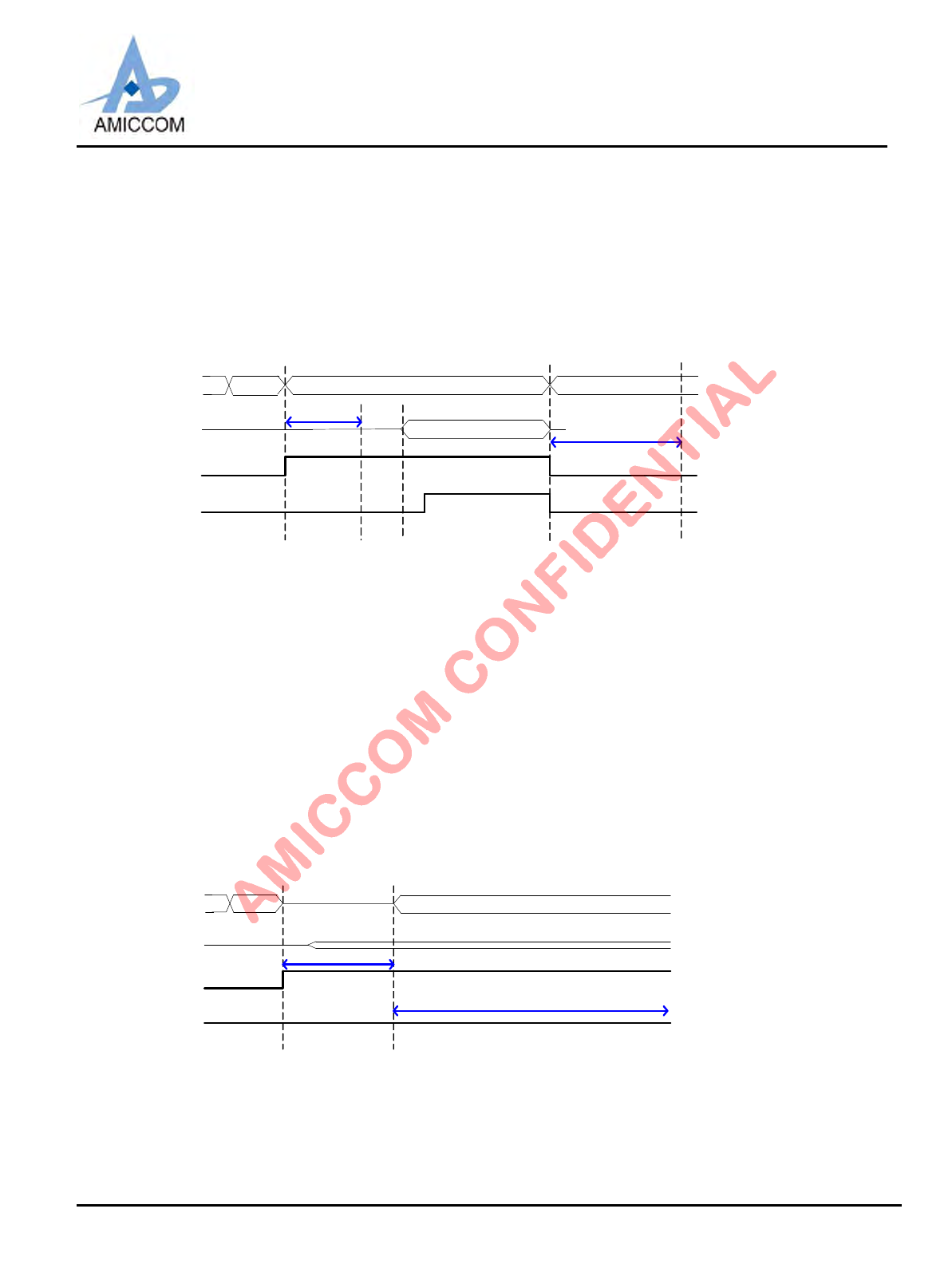
LBA7130
Oct., 2012, Version 0.6 (PRELIMINARY) 72 AMICCOM Electronics Corporation
Auto RSSI measurement for TX Power of the coming packet:
1. Set wanted FRXLO.
2. Set recommend values of Table 17.1.
3. Enable ADCM = 1.
4. Send RX Strobe command.
5. Once frame sync (FSYNC) is detected or exiting RX mode, user can read digital R SSI value from ADC [7:0] for TX power
of the coming packet.
Figure 17.2 RSSI Measurement of TX RSSI of the coming packet.
Auto RSSI measurement for Background Power:
1. Set wanted FRXLO.
2. Set recommend values of Table 17.1.
3. Enable ADCM = 1.
4. Send RX Strobe command.
5. Stay in RX mode at least 140 us and then exiting RX mode. User can read digital RSSI value from ADC [7:0] for the
background power.
Figure 17.3 Measurement of Background RSSI.
St robe CMD
(SCS,SCK,SDIO)
T0
RX Mode
T0-T1: Settling Time
T2-T3: Receiving Packet
T3 : Exit RX mode automatically in FIFO mode
T3-T4: MCU read RSSI value @ ADC [7:0]
T1
RX-Strobe
RX Ready Ti me
Received Packet
GIO1 Pin - WTR
(GPIO1S[3:0]=0000)
RF-IN
T2
GIO2 Pin - FSYNC
(GPIO2S[3:0]=0001)
T4
MCU Read ADC[7:0]
T3
Read 8 -bits RSSI value
Strobe CMD
(SCS,SCK,SDIO)
T0
T0-T1: MCU Delay Loop from PLL to RX mode for RSSI measurment
T1 : Auto RSSI Measurment is done by 8-times average.
MCU can read RSSI value from ADC [7:0]
RX-Strobe
Min. 140 us
No Packet
GIO1 Pin - WTR
(GPIO1S[3:0]=0000)
RFI Pin
T1
GIO2 Pin - FSYNC
(GPIO2S[3:0]=0001)
MCU Read ADC[7:0]
MCU reads 8-bits RSSI value that is refresh every 40 us

LBA7130
Oct., 2012, Version 0.6 (PRELIMINARY) 73 AMICCOM Electronics Corporation
18. Battery Detect
A7130 has a built-in battery detector to check supply voltage (REGI pin). The detecting range is 2.0V ~ 2.7V into 8 levels.
Battery detect Register (Address: 2Ch)
Name R/W Bit 7 Bit 6 Bit 5 Bit 4 Bit 3 Bit 2 Bit 1 Bit 0
WLVR RGV1 RGV0 QDS BVT2 BVT1 BVT0 BD_E
Battery detect R-- RGV1 RGV0 BDF BVT2 BVT1 BVT0 BD_E
BVT [2:0]: Battery voltage detect threshold.
[000]: 2.0V. [001]: 2.1V. [010]: 2.2V. [011]: 2.3V.
[100]: 2.4V. [101]: 2.5V. [110]: 2.6V. [111]: 2.7V.
BD_E: Battery Detect Enable.
[0]: Disable. [1]: Enable. It will be clear after battery detection is triggered.
BDF: Battery detection flag.
[0]: Battery voltage less than threshold. [1]: Battery voltage greater than threshold.
Below is the procedure to detect low voltage input (ex. below 2.1V):
1. Set A7130 in standby or PLL mode.
2. Set BVT [2:0] = [001] and enable BD_E = 1.
3. After 5 us, BD_E is auto clear.
4. User can read BDF or output BDF to GIO1 pin or CKO pin.
If REGI pin > 2.1V,
BDF = 1 (battery high). Else, BDF = 0 (battery low).
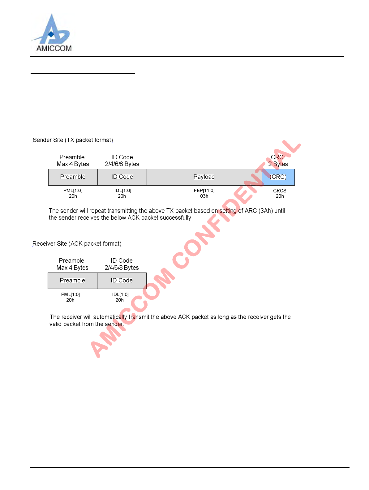
LBA7130
Oct., 2012, Version 0.6 (PRELIMINARY) 74 AMICCOM Electronics Corporation
19. Auto-ack and auto-resend
A7130 supports auto-resend and auto-ack scheme by enable EAK = 1 (auto-ack) and EAR = 1 (auto-resend). In application
points of view, this feature is also ok to enable together with other feature options like FCB and/or EDRL (dynamic FIFO).
19.1 Basic FIFO plus auto-ack auto-resend
Set EAF = 0, EAK = 1 and EAR = 1 to enable auto-ack and auto-resend. Please refer to the below TX and ACK packet format of
the sender and the receiver site respectively.
19.2 Advanced FIFO plus auto-ack and auto-resend
In addition to set EAF = 0, EAK = 1 and EAR = 1 to enable auto-ack and auto-resend. User can also enable an optional MAC
header (FCB field) in the TX packet together with auto-ack and auto resend scheme. Please refer to the below TX and ACK
packet format of the sender and the receiver site.
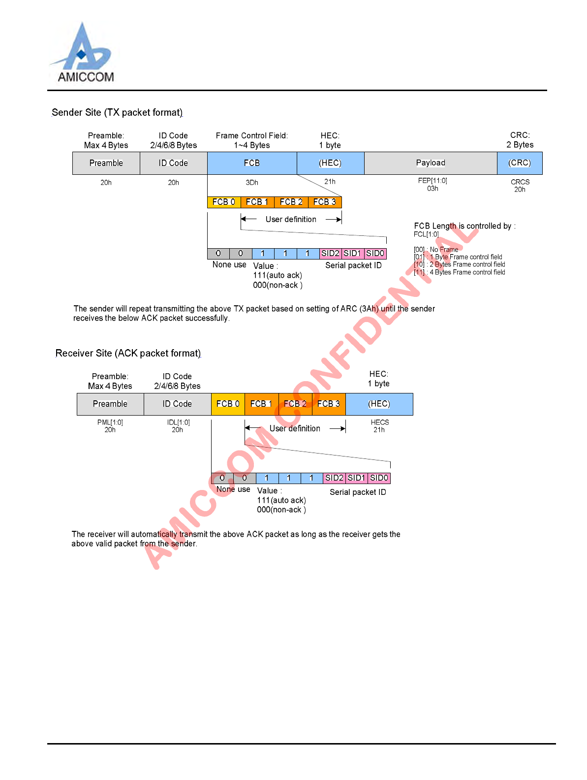
LBA7130
Oct., 2012, Version 0.6 (PRELIMINARY) 75 AMICCOM Electronics Corporation
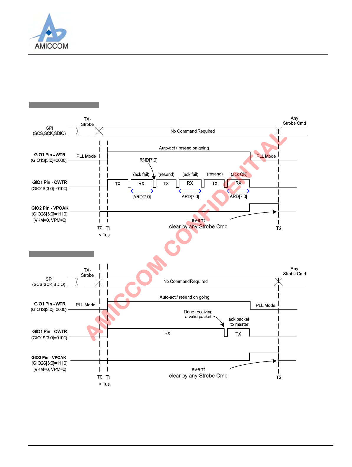
LBA7130
Oct., 2012, Version 0.6 (PRELIMINARY) 76 AMICCOM Electronics Corporation
19.3 WTR Behavior during auto-ack and auto-resend
If auto-ack and auto-resend are enabled (EAR = EAK = 1), WTR represents a completed transmission period and CWTR is a
debug signal which represents the cyclic TX period and cyclic RX period. Please refer to the below timing diagrams for details.
The sender site (auto-resend)
The receiver site (auto-ack)
Remark: Refer to 3Bh for ARD[7:0] setting (auto resend delay).
Refer to 3Fh for RND[7:0] setting (random seed for resend interval).
Refer to 3Ah for EAK (enable auto-ack).
Refer to 3Ah for EAR (enable auto-resend).
Refer to 0Bh for VKM and VPM.
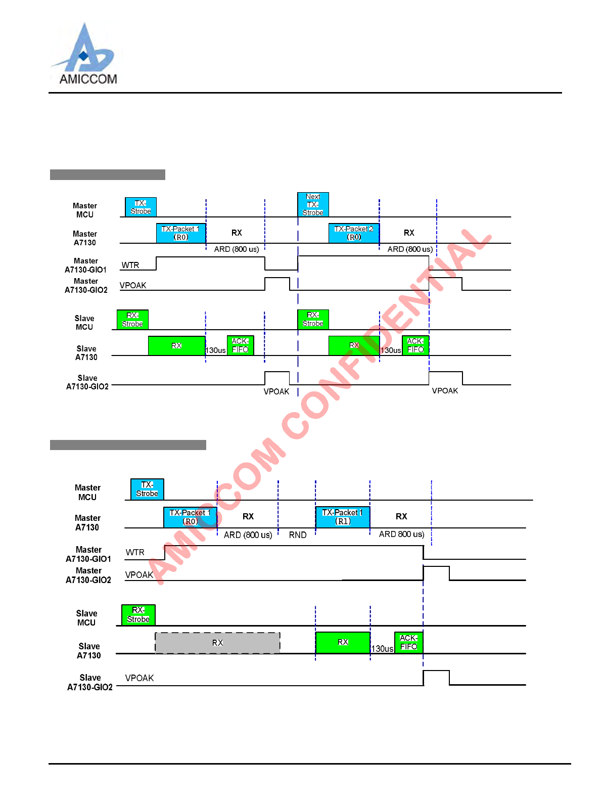
LBA7130
Oct., 2012, Version 0.6 (PRELIMINARY) 77 AMICCOM Electronics Corporation
19.6 Examples of auto-ack and auto-resend
Once EAK and EAR are enabled, below case 1 ~ case 3 illustrate the most common cases as a timing reference (assume ARD
= 800 us) in two ways radio communications.
<Case1> Always success
<Case2> Success in second packet
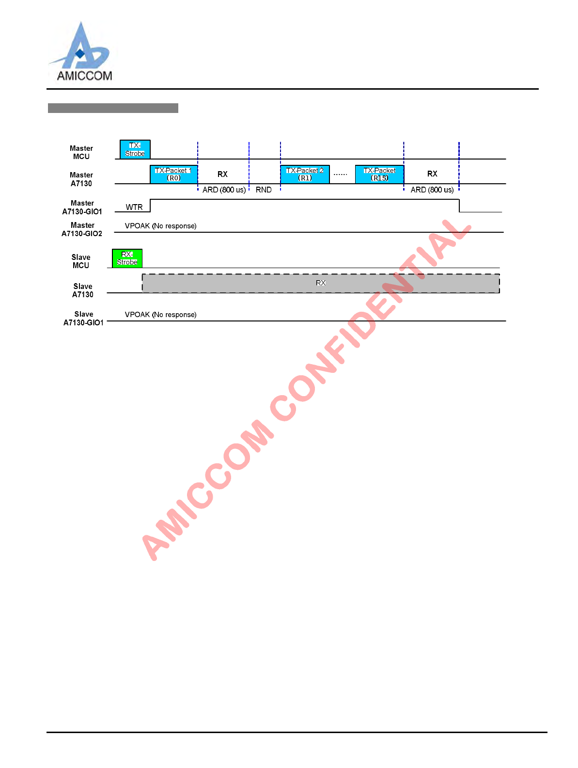
LBA7130
Oct., 2012, Version 0.6 (PRELIMINARY) 78 AMICCOM Electronics Corporation
<Case3> always resend failure
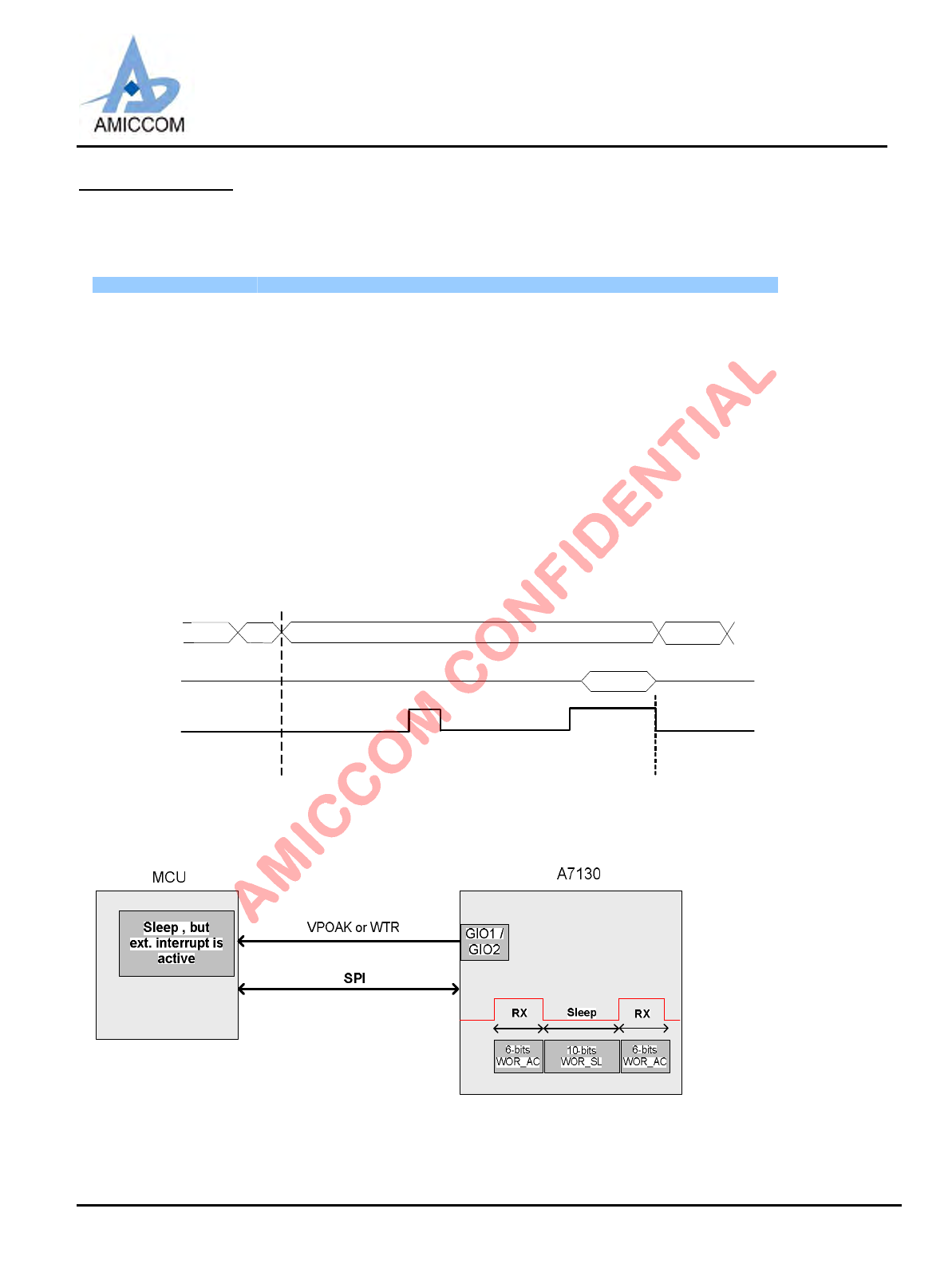
LBA7130
Oct., 2012, Version 0.6 (PRELIMINARY) 79 AMICCOM Electronics Corporation
20. RC Oscillator
A7130 has an internal RC oscillator to supports WOR (Wake On RX) and TWOR (Timer Wake On RX) function. RCOSC_E
(09h) is used to enable RC oscillator. WORE (01h) is used to enable WOR function and TWORE (09h) is used to enable TWOR
function. After done calibrations of RC oscillator, WOR and TWOR function can be operated from -40℃ to 85℃.
Parameter Min Max Unit Note
Calibrated Freq. 3.8K 4.2K Hz
Sleep period 7.82 8007.68 ms [( WOR_SL [9:0] ) +1] x 7.8 ms
RX period 0.244 ms [( WOR_AC [5:0] ) +1] x 244 us
Operation temperature -40 85 ℃After calibration.
20.1 WOR Function
When WOR is enabled (WORE = 1 and RCOSC_E =1), A7130 periodically wakes up f rom sleep and li sten (auto-enter RX
mode) for incoming packets without MCU interaction. Therefore, A7130 will stay in sleep mode based on WOR_SL timer and
RX mode based on WOR_AC timer unless a packet is received.
The internal RC oscillator used for the WOR function varies with temperature and CMOS process deviation. In order to keep the
frequency as accurate as possible, the RC oscillator shall be calibrated (CALWC=1) whenever possible. After done calibrations,
MCU shall set WORE=1 and issue sleep strobe command to start WOR function. After a period (WOR_SL) in sleep mode, the
device goes to RX mode to check coming packets. And then, A7130 is back to sleep mode for the next WOR cycle. To end up
WOR function, MCU just needs to set WORE = 0. Beware, please turn on MSCRC (21h, CRC data filtering) when CRCS = 1
(20h, CRC select) in WOR function.
Strobe CMD
(SCS,SCK,SDIO) No Command Required
sleep
GIO1 -- WTR
GIO1S[3:0]=0000
RF In Pin
Strobe
cmd
Sleep
WOR_SL[9:0]
RX Sleep
WOT_SL[9:0]
RX
Start WOR
(sleep strobe)
Coming
packet
End of WOR
(set WORE = 0)
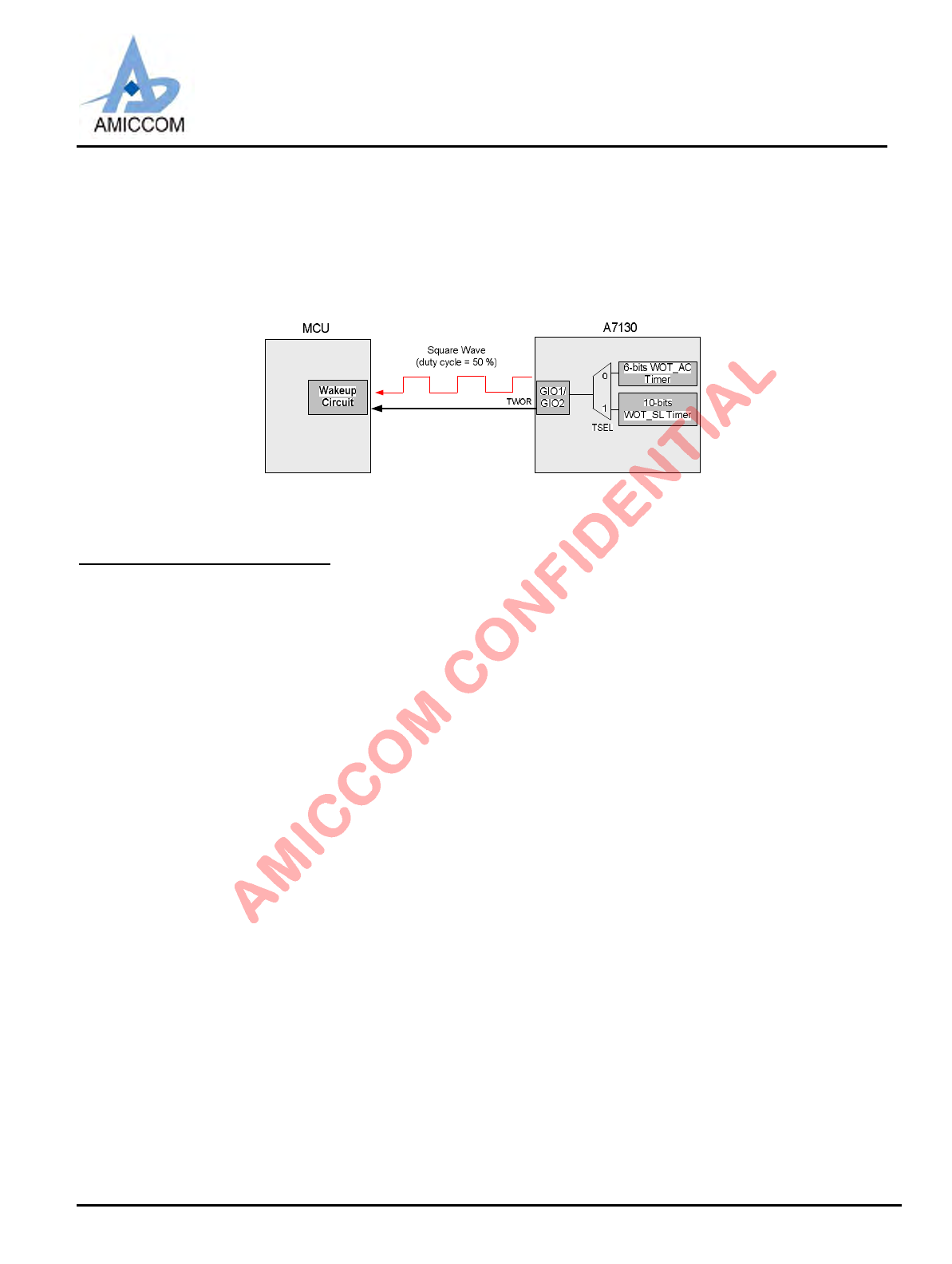
LBA7130
Oct., 2012, Version 0.6 (PRELIMINARY) 80 AMICCOM Electronics Corporation
20.2 TWOR Function
The RC oscillator inside A7130 can also be used to supports programmable TWOR (Timer Wake-On, TWORE=1) function
which enables A7130 to output a periodic square wave from GIO1 (or GIO2). The duty cycle of this square wave is set by
WOR_AC (08h) or WOR_SL (08h and 07h) regarding to TSEL (09h). User can use this square wave to wake up MCU or other
purposes.
21. AES128 Security Packet
A7130 has a built-in AES128 co-processor to generate a security packet by a general purpose MCU. In addition to support
128-bits key length (AES128), A7130 also support a proprietary 32-bits key length called AES32.
Software procedure to use AES128.
Step1: Write 16-bytes AES128 key to KEYI [127:0] (36h)
Step2: Set AESS=1 (3Eh) to select standard AES128
Step3. Set AKFS=0 (3Eh) to disable attaching AES128 KEYI [127:0] into the TX packet.
Step4: Set EDCRS=1 (3Eh) to enable AES co-processor.
Step5: Write plain text to TX FIFO
Step6: Issue TX strobe command and then A7130 will execute AES128 encryption and deliver the cipher text without latency.
Step7: In RX side with the same configurations, A7130 will execute AES128 decryption and store plain text back to RX FIFO.
Remark
1. The unit size of AES128 encryption packet is 16-bytes.
2. In TX side, if plain text is not dividable by 16-bytes, i.e. 5-bytes only, the TX packet is complement to be 16-bytes.
3. In RX side, the coming cipher text will be decrypted and restore 5-bytes plain text back to RX FIFO.
Software procedure to use AES32.
Step1: Write 4-bytes AES128 key to KEYI [31:0] (36h)
Step2: Set AESS=0 (3Eh) to select proprietary AES32.
Step3. Set AKFS=0 (3Eh) to not attach AES128 KEYI [31:0] to the wanted TX packet.
Step4: Set EDCRS=1 (3Eh) to enable AES co-processor.
Step5: Write plain text to TX FIFO
Step6: Issue TX strobe command and then A7130 will execute AES32 encryption and deliver the cipher text without latency.
Step7: In RX side with the same configurations, A7130 will execute AES32 decryption and store plain text back to RX FIFO.
Remark
1. The unit size of AES32 encryption packet is 4-bytes.
2. In TX side, if plain text is not dividable by 4-bytes, i.e. 5-bytes only, the TX packet is complement to 8-bytes.
3. In RX side, the coming cipher text will be decrypted and restore 5-bytes plain text back to RX FIFO.
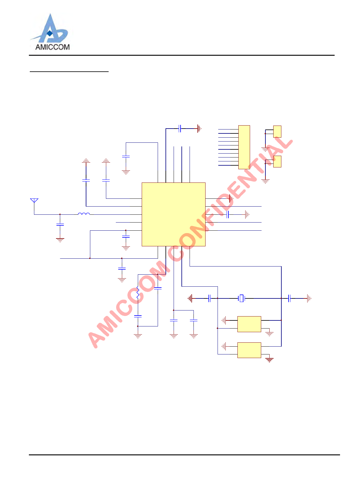
LBA7130
Oct., 2012, Version 0.6 (PRELIMINARY) 81 AMICCOM Electronics Corporation
22. Application circuit
22.1 MD70-A01
AMICCOM’s ref. design module, MD7130-A01, max 5 dBm output power, application circuit example.
C1
470pF
SCS
C2
100pF
C5
100pF
VDD_A
C6
0.1uF
R1
NC
SCK
C9
NC
SDIO
C8
2.2nF
G I O1
CKO
G I O2
G ND
G ND
VIN
G ND
C10
0.1uF
1
2
3
4
5
6
7
8
9
10
J1
CON/10P 2.0
1
2J2
CON/2P 2.0
C12
NC
1
2J3
CON/2P 2.0
C13
NC
C7
2.2uF
SDIO
SCK
SCS
VDD_A
TP1
ANTENNA
CKO
GIO2
GIO1
V IN
C15
1.8pF
ANT
C4 2.2uF
L2
2.7nH
C3
4.7uF
VDD_A
C11
100pF 1
3
G ND 2
G ND
4
Y2 NC
1
3
G ND 2
G ND
4
Y3
16M Hz XTA L_ 3. 2*2. 5
Y1 NC
BP_RSSI
1
BP_BG
2
RFI
3
RFC
5
RFO
4
V DD _ VCO
6
CP
7
VDD_PLL
8
XI
9
XO
10
GND 15
SCS 11
SCK 12
SDIO 14
VDD_D 13
CKO 18
GIO2 17
GIO1 16
REGI 19
VDD_A 20
A7130PKG
U1
A7130
Remark
1. RF Matching to 50Ω.
2. RX and TX signal are combined internally to RFI pin only so that RFSP bit = 0 (DASP0 register = 0x34).
3. Recommend 16MHz crystal with 18 pF Cload.
4. Recommend to let C12 and C13 NC because of enabling on-chip Xtal Capacitors by (INTXC = 1 and CSXTAL = [10100]).
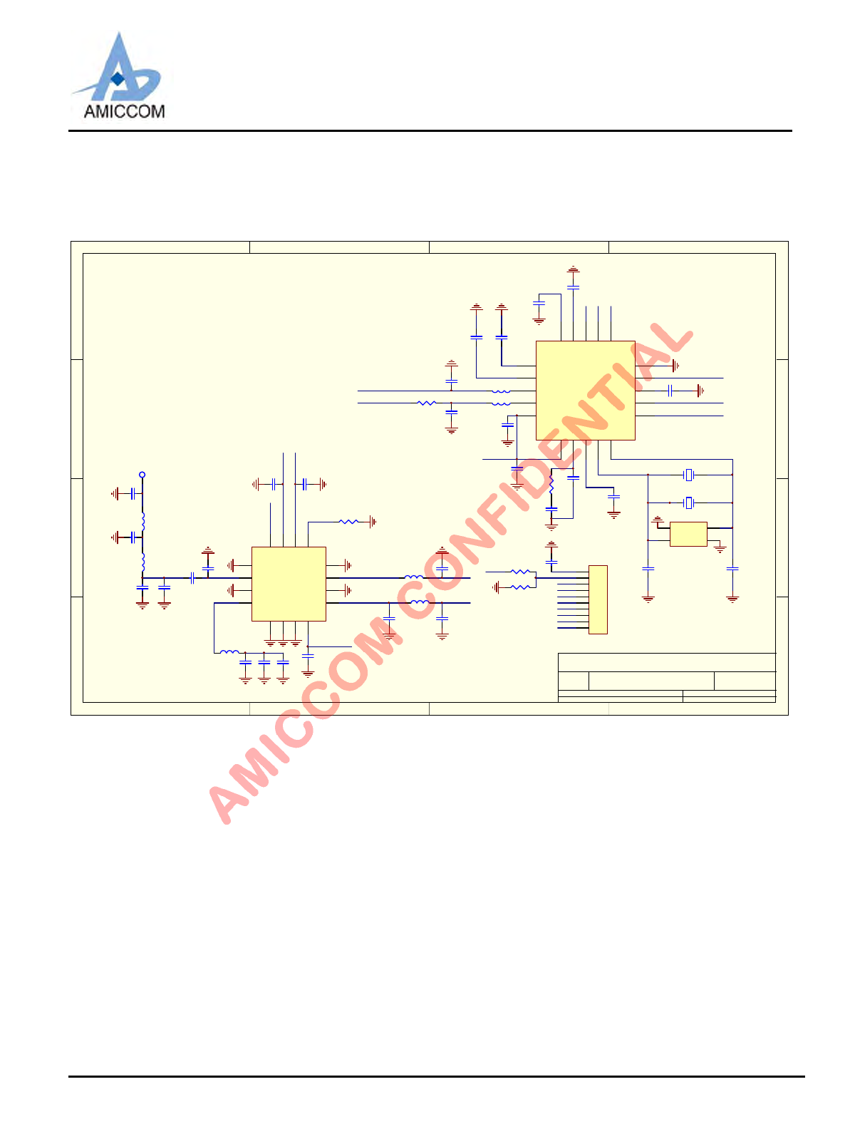
LBA7130
Oct., 2012, Version 0.6 (PRELIMINARY) 82 AMICCOM Electronics Corporation
22.2 MD70-F07
AMICCOM’s ref. design module, MD7130-F07, typical 17 dBm output power together with a range extendor A7700.
1 2 3 4
A
B
C
D
4321
D
C
B
ATitle
Numbe r Revi si onSize
A4
Dat e: 1 2- Ja n-2 012 S he et o f
File: C:\Docu ment s and Sett ings\ac008 6\桌面\MD7130~2.DDBDrawn By:
MD7˄ˆ0-F07-05(2L)
SCS
SCK
SDIO
GIO1
GIO2
CKO or GND
GND
REGI33 1
2
3
4
5
6
7
8
9
10
J2
CON/10P 2.0
C2
100pF
VDD_A
C29
100pF
R10
NC
C32
NC
C31
2.2nF C30
0.1uF
C14
0.1uF 1 2
Y1
16MHz
C20
2.2uF
SDIO
SCK
SCS
C5
4.7uF
VDD_A
CKO
GIO2
GIO1
R E GI 33
C18
2.2uF
VDD_A
LNA_OUT
PA_IN
C13
0.1uF
C57
100pF
REGI33
R6
6.8K
REGI 33
C36
NC
L2
3nH
C3 8 NC
C9
1.2pF
TRX
RFI
RFO
BG
C33
8.2pF
C25 1pF
LNA_OUT
PA_IN
C42
NC
REGI33
VDD_PA
C7
8.2pF
L1
4.7nH
C8
NC
ANT
2
GND
1
VDD_PA
4
GND
5
VDD_BA
7
V DD _A
8
RFI 9
RFO 11
BG 13
RX SW 15
TX SW 14
HGM 16
NC
3
NC
6
GND 10
BGS 12
U2
A7700
TX SW
RX SW
2012.01.12
C1
2.2pF
L3
0R
TP1
TEST POINT
C19
1.5pF
C6
1.5pF
C11
NC
L7
2.4nH
L8
2.4nH R11 NC
R12 0R
CKO
L9 3.3nH
L10 3.3nH
C10
1pF
C16
1pF
C3
1nF
BP_RSSI
1
BP_ BG
2
RFI
3
RFC
5
RFO
4
VDD_VCO
6
CP
7
VDD_PLL
8
XI
9
XO
10
GND 15
SCS 11
SCK 12
SDIO 14
VDD_D 13
CKO 18
GIO2 17
GIO1 16
RE GI 19
VDD_A 20
A7130 PKG
U1
A70
TX SW
RX SW
C12
NC
C15
NC
C34
NC C37
NC
1 2
Y2 16MHz
1
3
GND 2
GND
4
Y3
CRYSTAL/5*3.2
R1
47
Remark
1. RF matching to 50Ω.
2. RX and TX signal are separated to RFI pin and RFO pin so that RFSP bit = 1 (DASP0 register = 0x74).
3. Recommend 16MHz crystal with 18 pF Cload.
4. Recommend to let C34 and C37 NC because of enabling on-chip Xtal Capacitors by (INTXC = 1 and CSXTAL = [10100]).
LBA7130
Oct., 2012, Version 0.6 (PRELIMINARY) 83 AMICCOM Electronics Corporation
23. Abbreviations
ADC Analog to Digital Converter
AIF Auto IF
FC Frequency Compensation
AGC Automatic Gain Control
BER Bit Error Rate
BW Bandwidth
CD Carrier Detect
CHSP Channel Step
CRC Cyclic Redundancy Check
DC Direct Current
FEC Forward Error Correction
FIFO First in First out
FSK Frequency Shift Keying
ID Identifier
IF Intermediate Frequency
ISM Industrial, Scientific and Medical
LO Local Oscillator
MCU Micro Controller Unit
PFD Phase Frequency Detector for PLL
PLL Phase Lock Loop
POR Power on Reset
RX Receiver
RXLO Receiver Local Oscillator
RSSI Received Signal Strength Indicator
SPI Serial to Parallel Interface
SYCK System Clock for digital circuit
TX Transmitter
TXRF Transmitter Radio Frequency
VCO Voltage Controlled Oscillator
XOSC Crystal Oscillator
XREF Crystal Reference frequency
XTAL Crystal
24. Ordering Information
Part No. Package Units Per Reel / Tray
A71C30AQFI/Q QFN20L, Pb Free, Tape & Reel, -40℃〜85℃3K
A71C30AQFI QFN20L, Pb Free, Tray, -40℃〜85℃490EA
A71C30AH Die form, -40℃〜85℃100EA
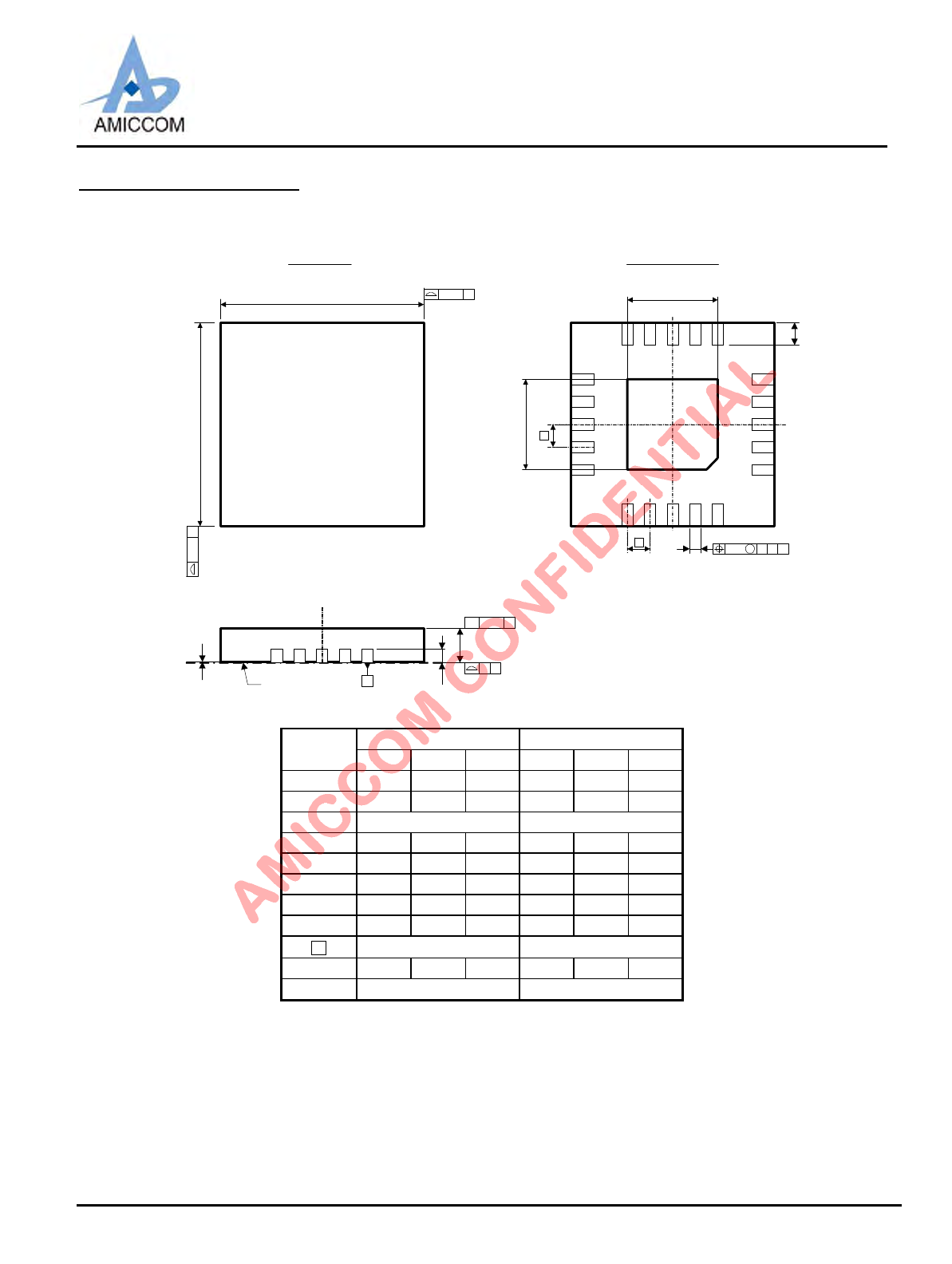
LBA7130
Oct., 2012, Version 0.6 (PRELIMINARY) 84 AMICCOM Electronics Corporation
25. Package Information
QFN 20L (4 X 4 X 0.8mm) Outline Dimensions
11
16
20
10
6
15
1 5
0.25 C
0.25 C
D
E
D2
E2
e
11 15
16
20
5 1
ebC0.10 MA B
10
6
L
TOP VIEW BOTTOM VIEW
A1
C
A3
A
0.10// C
y C
Seating Plane
Dimensions in inches Dimensions in mm
Symbol
Min Nom Max Min Nom Max
A 0.028 0.030 0.032 0.70 0.75 0.80
A10.000 0.001 0.002 0.00 0.02 0.05
A30.008 REF 0.203 REF
b0.007 0.010 0.012 0.18 0.25 0.30
D0.154 0.158 0.161 3.90 4.00 4.10
D20.075 0.079 0.083 1.90 2.00 2.10
E0.154 0.158 0.161 3.90 4.00 4.10
E20.075 0.079 0.083 1.90 2.00 2.10
e0.020 BSC 0.50 BSC
L0.012 0.016 0.020 0.30 0.40 0.50
y0.003 0.08
LBA7130
Oct., 2012, Version 0.6 (PRELIMINARY) 85 AMICCOM Electronics Corporation
26. Top Marking Information
A71C30AQFI
A : 0.55
B : 0.36
C1 : 0.25 C2 : 0.3
C3 : 0.2
D : 0.03
F=G
I=J
K=L
YYWW:DATECODE
: PKG HOUSE
ID
: LOT NO.
(max. 9 characters)
N N N N N N
X
v
CHARACTER SIZE : (Unit in mm)
0.8
0
0.6
8
70
1.6
0
0.6
5
J
70
C1
KL
C2
D
A
YYWX
W
BI
NNNNN
N
C3
NNN
NN N
FG
¡Part No. :A71C30AQFI
¡ Pin Count :20
¡ Package Type : QFN
¡ Dimension :4*4 mm
¡ Mark Method : Laser Mark
¡ Character Type : Arial
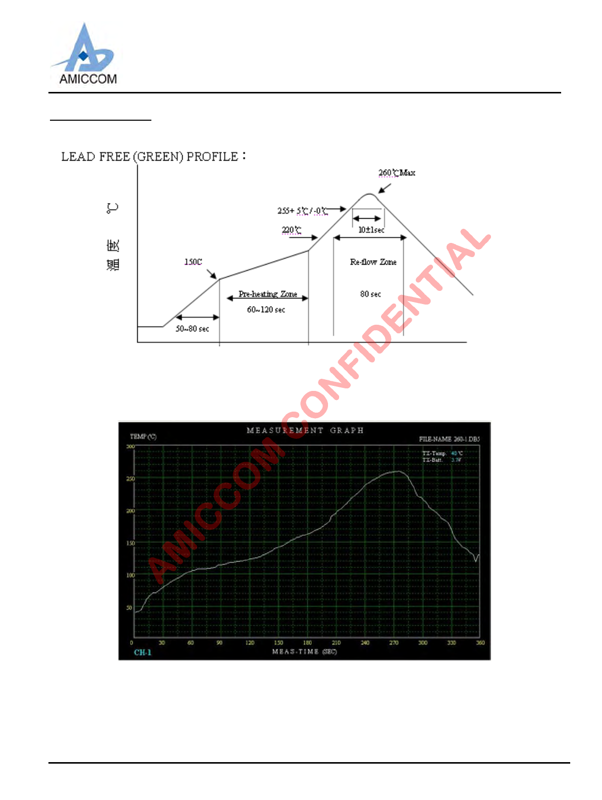
LBA7130
Oct., 2012, Version 0.6 (PRELIMINARY) 86 AMICCOM Electronics Corporation
27. Reflow Profile
Actual Measurement Graph
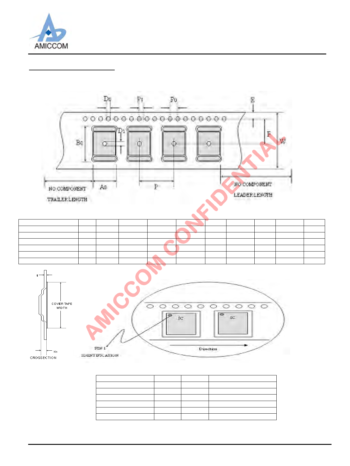
LBA7130
Oct., 2012, Version 0.6 (PRELIMINARY) 87 AMICCOM Electronics Corporation
28. Tape Reel Information
Cover / Carrier Tape Dimension
Unit: mm
TYPE P A0 B0 P0 P1 D0 D1 E F W
20 QFN 4*4 8 4.35 4.35 4.0 2.0 1.5 1.5 1.75 5.5 12
24 QFN 4*4 8 4.4 4.4 4.0 2.0 1.5 1.5 1.75 5.5 12
32 QFN 5*5 8 5.25 5.25 4.0 2.0 1.5 1.5 1.75 5.5 12
QFN3*3 / DFN-10 4 3.2 3.2 4.0 2.0 1.5 - 1.75 1.9 8
20 SSOP 12 8.2 7.5 4.0 2.0 1.5 1.5 1.75 7.5 16
24 SSOP 12 8.2 8.8 4.0 2.0 1.5 1.5 1.75 7.5 16
TYPE K0 t COVER TAPE WIDTH
20 QFN (4X4) 1.1 0.3 9.2
24 QFN (4X4) 1.4 0.3 9.2
32 QFN (5X5) 1.1 0.3 9.2
QFN3*3 / DFN-10 0.75 0.25 8
20 SSOP 2.5 0.3 13.3
24 SSOP 2.1 0.3 13.3
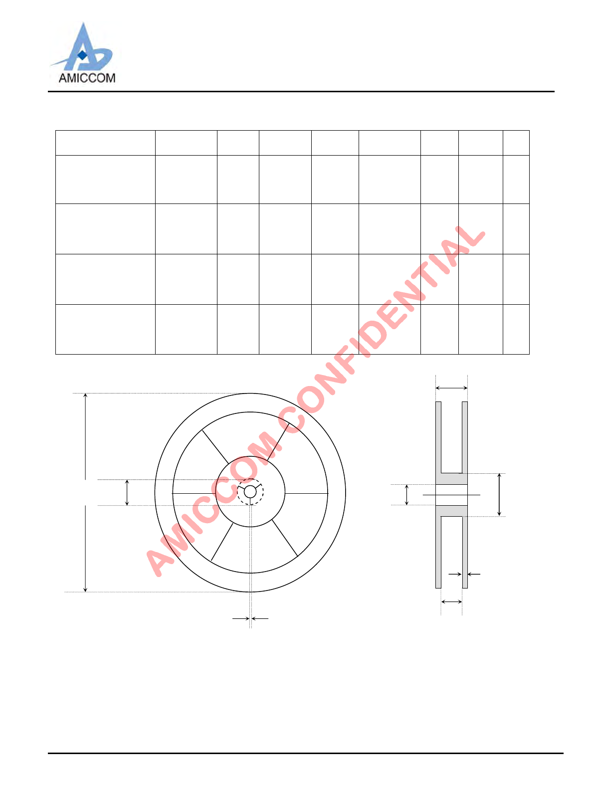
LBA7130
Oct., 2012, Version 0.6 (PRELIMINARY) 88 AMICCOM Electronics Corporation
REEL DIMENSIONS
UNIT IN mm
TYPE G N T M D K L R
20 QFN(4X4)
24 QFN(4X4)
32 QFN(5X5)
DFN-10
12.8+0.6/-0.4 100
REF 18.2(MAX) 1.75±0.25 13.0+0.5/-0.2 2.0±0.5 330+
0.00/-1.0 20.2
48 QFN(7X7) 16.8+0.6/-0.4
100
REF
22.2(MAX) 1.75±0.25 13.0+0.5/-0.2 2.0±0.5
330+
0.00/-1.0 20.2
28 SSOP (150mil) 20.4+0.6/-0.4
100
REF
25(MAX) 1.75±0.25 13.0+0.5/-0.2 2.0±0.5
330+
0.00/-1.0 20.2
20 SSOP
24 SSOP 16.4+2.0/-0.0
100
REF
22.4(MAX) 1.75±0.25 13.0+0.2/-0.2 1.9±0.4
330+
0.00/-1.0 20.2
N
M
G
D
T
L R
K
LBA7130
Oct., 2012, Version 0.6 (PRELIMINARY) 89 AMICCOM Electronics Corporation
RF ICs
AMICCOM
29. Product Status
Data Sheet Identification Product Status Definition
Objective Planned or Under Development This data sheet contains the design specifications
for product development. Specifications may
change in any manner without notice.
Preliminary Engineering Samples
and First Production
This data sheet contains preliminary data, and
supplementary data will be published at a later
date. AMICCOM reserves the right to make
changes at any time without notice in order to
improve design and supply the best possible
product.
No Identification Noted Full Production This data sheet contains the final specifications.
AMICCOM reserves the right to make changes at
any time without notice in order to improve design
and supply the best possible product.
Obsolete Not In Production This data sheet contains specifications on a
product that has been discontinued by AMICCOM.
The data sheet is printed for reference information
only.
Headquarter
A3, 1F, No.1, Li-Hsin Rd. 1, Hsinchu Science Park,
Taiwan 30078
Tel: 886-3-5785818
Shenzhen Office
Rm., 2003, DongFeng Building, No. 2010,
Shennan Zhonglu Rd., Futian Dist., Shenzhen, China
Post code: 518031
Web Site
http://www.amiccom.com.tw
Modular Approal:
The LBA 7130RF module is designed to comply with the FCC statement. FCC ID is OIE51402TR.
The host system using LBA 7130RF, should have label indicated FCC ID: OIE51402TR.
This radio module must not installed to co-locate and operating
Simultaneously with other radios in host system, additional testing
and equipment authorization may be required to operating simultaneously with other radio
FCC Statement:
1. This device complies with Part 15 of the FCC Rules. Operation is subject to the following two
conditions:
(1)This device may not cause harmful interference, and
(2)This device must accept any interference received, including interference that may cause
undesired operation.
2. Changes or modifications not expressly approved by the party responsible for compliance
could void the user’s authority to operate the equipment.