LG Electronics USA 9QK-DMWB1NP6 Bluetooth Adapter Card User Manual
LG Electronics USA Bluetooth Adapter Card
UserManual.wiki
>
LG Electronics USA
>
9QK DMWB1NP6 User Manual
User Manual
Navigation menu
Upload a User Manual
Namespaces
Wiki Guide
HTML
PDF
Info
Views
User Manual
Discussion / Help
Navigation
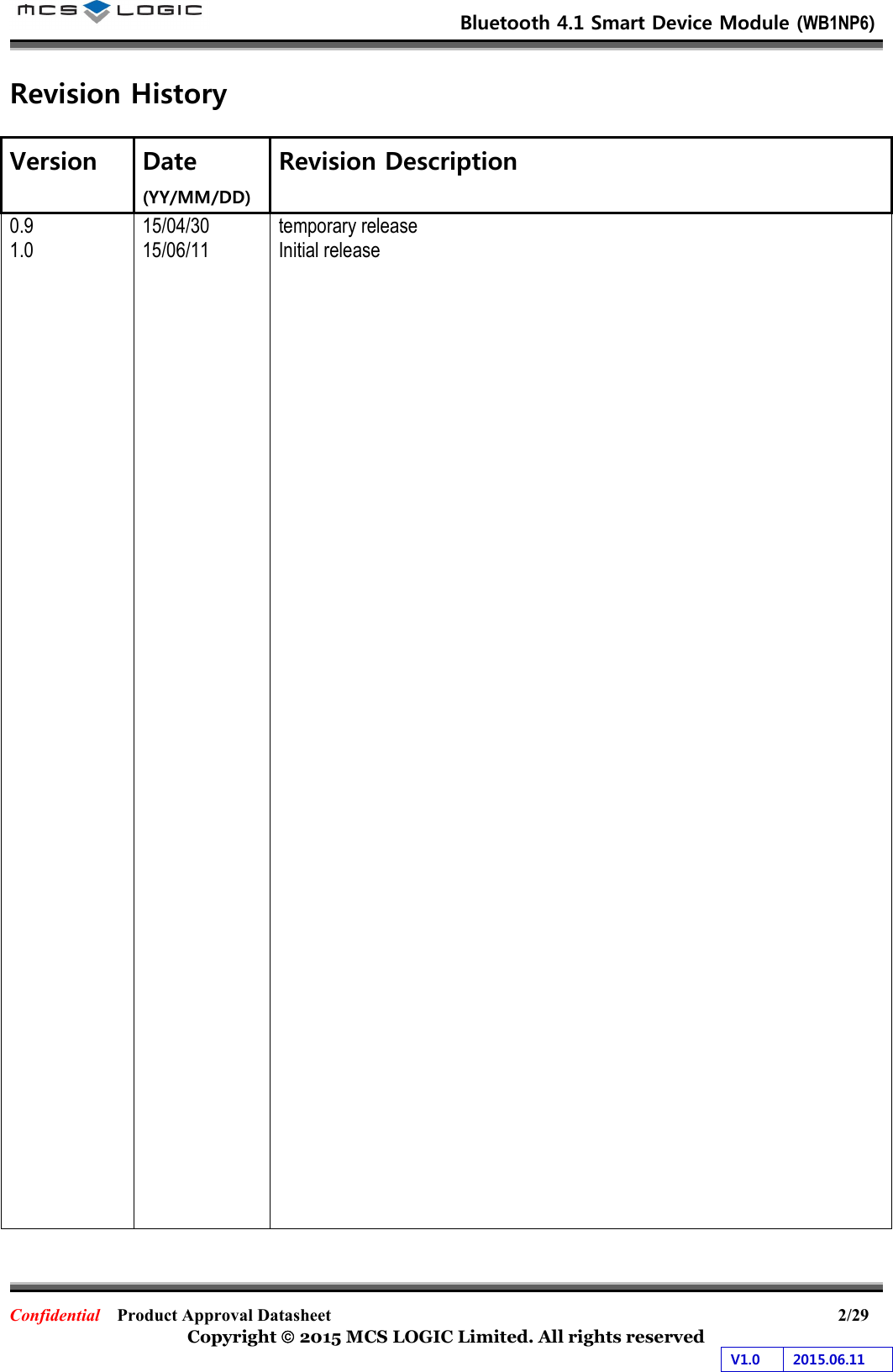
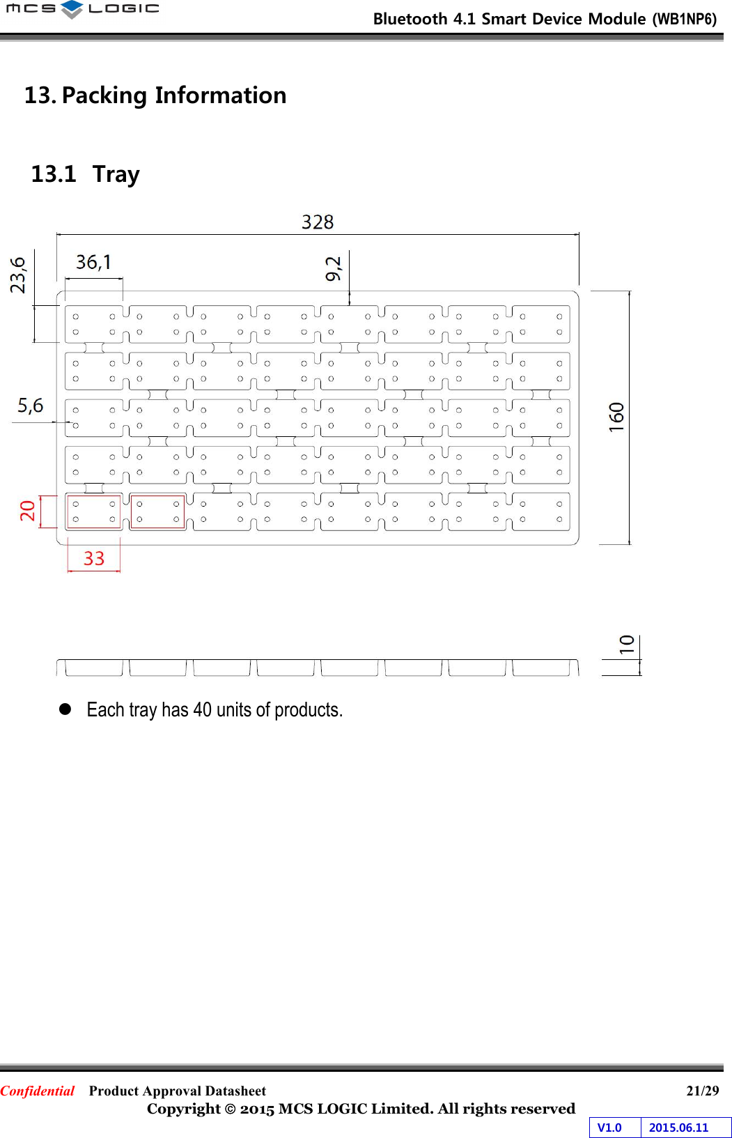
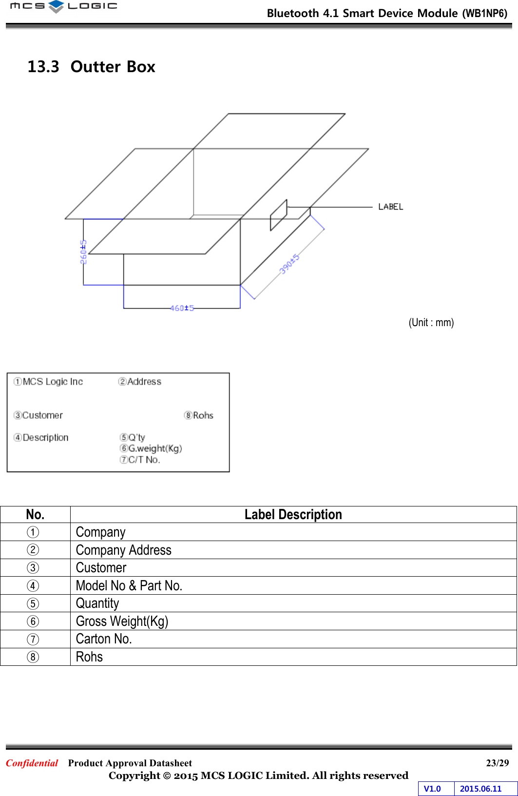
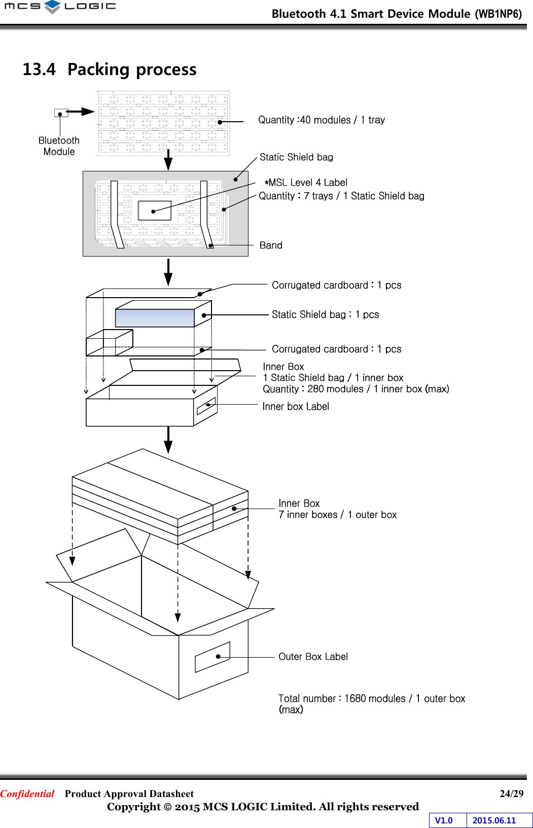
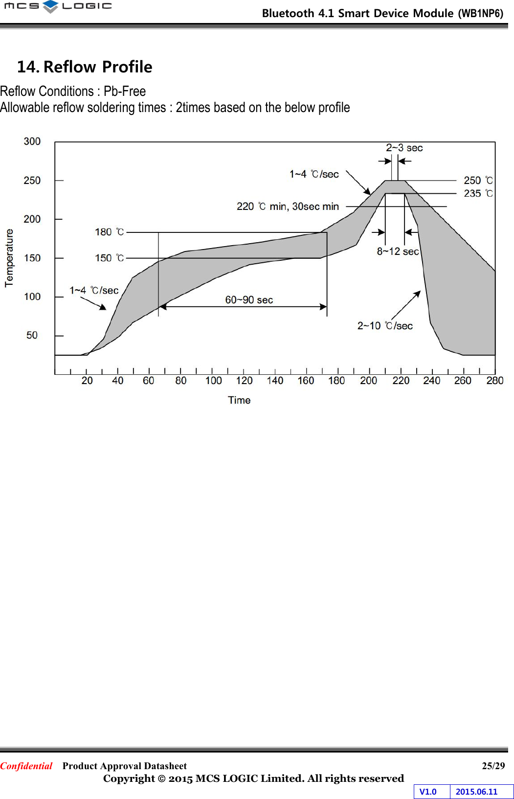
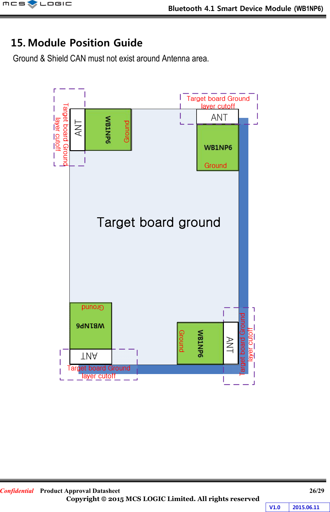
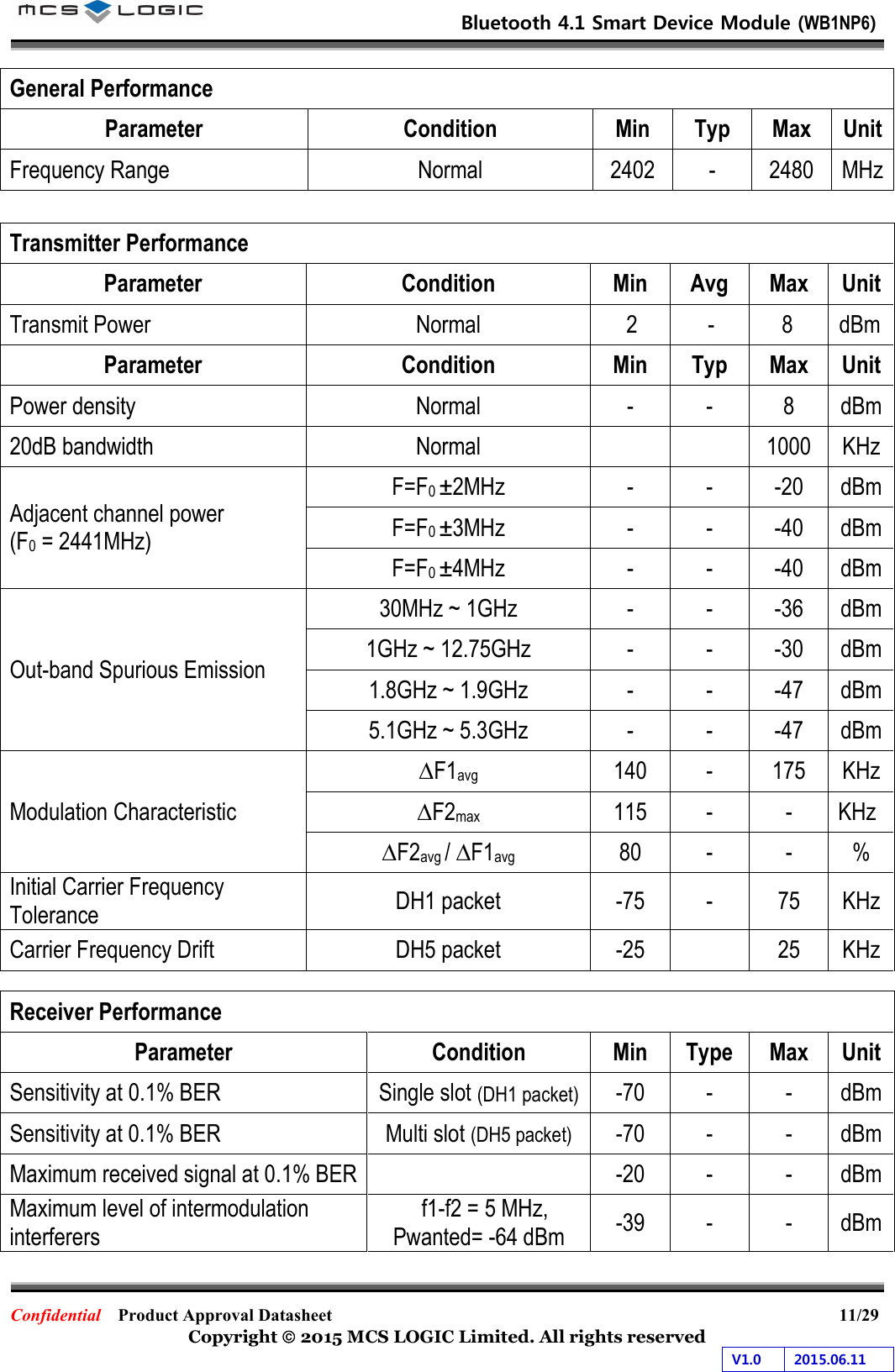
![Bluetooth 4.1 Smart Device Module (WB1NP6) Confidential Product Approval Datasheet 7/29 Copyright 2015 MCS LOGIC Limited. All rights reserved V1.0 2015.06.11 No Pin Name I/O Description 1 GND I CON CONNECTION FOR AUDIO 2 MIC_LP I MIC INPUT POSITIVIE LEFT 3 MIC_LN I MIC INPUT NEGATIVE LEFT 4 MIC_BIAS_A O MIC BIAS A 5 MIC_BIAS_B O MIC BIAS B 6 MIC_RN I MIC INPUT NEGATIVE RIGHT 7 MIC_RP I MIC INPUT POSITIVIE RIGHT 8 GND I GND CONNECTION FOR INTERNAL DIGITAL CIRCUITTRY AND PADS 9 PCM_IN I/O SYNCHRONOUS DATA INPUT, Alternative function PIO[17] 10 PCM_CLK I/O SYNCHRONOUS DATA CLOCK, Alternative function PIO[20] 11 PCM_OUT I/O SYNCHRONOUS DATA OUTPUT, Alternative function PIO[18] 12 PCM_SYNC I/O SYNCHRONOUS DATA SYNC, Alternative function PIO[19] 13 SPI_CLK I SPI CLOCK 14 SPI_MOSI I SPI DATA INPUT 15 SPI_MISO O SPI DATA OUTPUT 16 SPI_CS# I CHIP SELECT FOR SPI, ACTIVE LOW 17 AIO[0] I AIO 18 AIO[1] I AIO 19 VDD_USB I POSITIVE SUPPLY FOR USB PORT 20 USB_N I/O USB DATA MINUS 21 USB_P I/O USB DATA PLUS 22 VDD_PADS_1 I 1.7~3.6V SUPPLY INPUT FOR IO PORTS (RST#, UART, PCM, SPI, PIO[3:0] 23 RST# I RESET IF LOW (>5ms) 24 LED[0] O LED DRIVER 25 LED[2] O LED DRIVER 26 LED[1] O LED DRIVER 27 GND I GND CONNECTION FOR INTERNAL DIGITAL CIRCUITTRY AND PADS 28 UART_RTS I/O UART REQUEST TO SEND, ACTIVE LOW, Alternative function PIO[16] 29 UART_RX I UART DATA IN 30 UART_CTS I/O UART CLEAR TO SEND, ACTIVE LOW 31 UART_TX O UART DATA OUT 32 PIO[0] I/O GPIO 33 PIO[1] I/O GPIO 34 PIO[2] I/O GPIO 35 PIO[15] I/O GPIO 36 PIO[7] I/O GPIO 37 PIO[6] I/O GPIO 38 VDD_PADS_2 I 1.7~3.6V SUPPLY INPUT FOR PIO[15:4] 39 PIO[3] I/O GPIO](https://usermanual.wiki/LG-Electronics-USA/9QK-DMWB1NP6/User-Guide-2659733-Page-5.png)
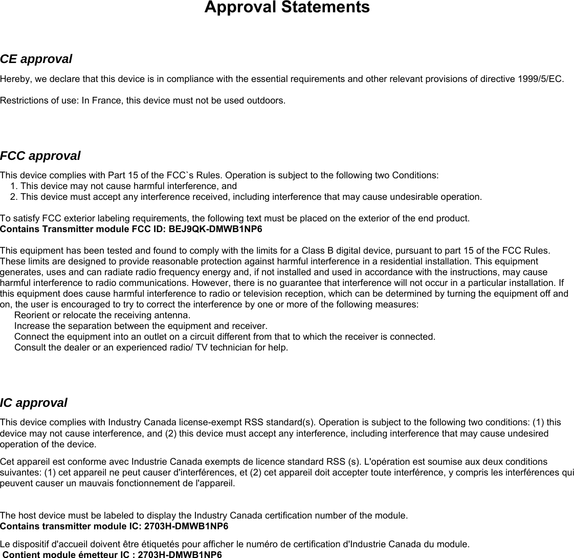
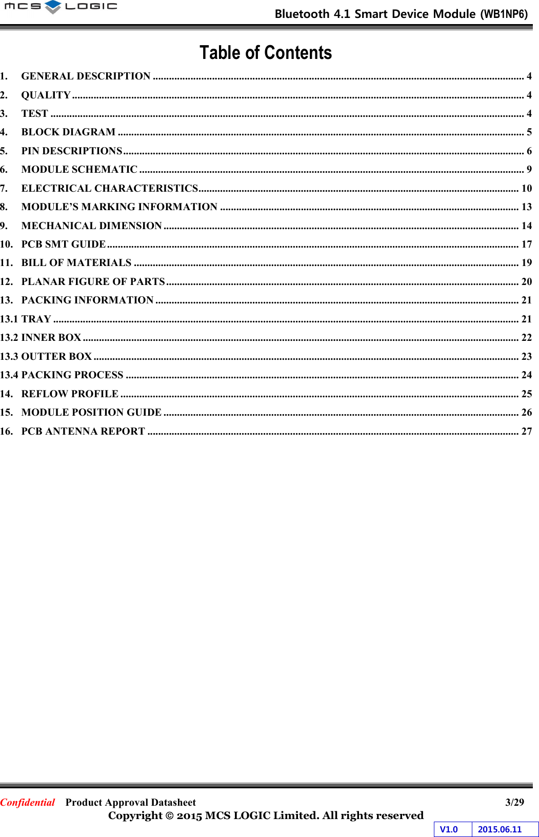
![Bluetooth 4.1 Smart Device Module (WB1NP6) Confidential Product Approval Datasheet 8/29 Copyright 2015 MCS LOGIC Limited. All rights reserved V1.0 2015.06.11 40 PIO[14] I/O GPIO 41 PIO[5] I/O GPIO 42 PIO[10] I/O GPIO 43 PIO[4] I/O GPIO 44 GND I GND CONNECTION FOR INTERNAL DIGITAL CIRCUITTRY AND PADS 45 PIO[11] I/O GPIO 46 PIO[12] I/O GPIO 47 PIO[13] I/O GPIO 48 QSPI_FLASH_IO3 I/O SERIAL QUAD IO FLASH DATA BIT 3, Alternative function PIO[28] 49 QSPI_FLASH_CS# I/O SPI FLASH CHIP SELECT, , Alternative function PIO[23] 50 QSPI_FLASH_CLK I/O SPI FLASH CLOCK, Alternative function PIO[21] 51 QSPI_FLASH_IO0 I/O SERIAL QUAD IO FLASH DATA BIT 0, Alternative function PIO[25] 52 QSPI_SPAM_CLK I/O SPI RAM CLOCK, Alternative function PIO[22] 53 QSPI_FLASH_IO1 I/O SERIAL QUAD IO FLASH DATA BIT 1, Alternative function PIO[26] 54 QSPI_FLASH_IO2 I/O SERIAL QUAD IO FLASH DATA BIT 2, Alternative function PIO[27] 55 QSPI_SRAM_CS# I/O SPI RAM CHIP SELECT, Alternative function PIO[24] 56 1V8_SMPS O 1.8V REGULATOR OUTPUT 57 VBAT_SENSE I BATTERY CHARGER SENSE INPUT 58 VBATT I BATTERY POSITIVE TERMINAL 59 VBUS I BATTERY CHARGER INPUT 60 3V3_OUT O ALTERMATIVE SUPPLY VIA BYPASS REGULATOR FOR 1.8V AND 1.35V REGULATOR INPUTS. MUSET BE THE SAME POTENTIAL AS VBAT. 61 CHG_EXT I EXTERNAL BATTERY CHARGER CONTROL 62 GND I GND CONNECTION FOR AUDIO DRIVER 63 SPKR_LP O SPEAKER OUTPUT POSITIVE LEFT 64 SPKR_LN O SPEAKER OUTPUT NEGATIVE LEFT 65 SPKR_RP O SPEAKER OUTPUT POSITIVE RIGHT 66 SPKR_RN O SPEAKER OUTPUT NEGATIVE RIGHT 67 GND I 1.35V REGULATOR GND 68 VRGEG_EN I REGULATOR ENABLE INPUT 69 VDD_PADS_3 I 1.7V~3.6V SUPPLY INPUT FOR RERIAL QUAD IO FLASH PORT 70 GND I 1.8V REGULATOR GND](https://usermanual.wiki/LG-Electronics-USA/9QK-DMWB1NP6/User-Guide-2659733-Page-6.png)
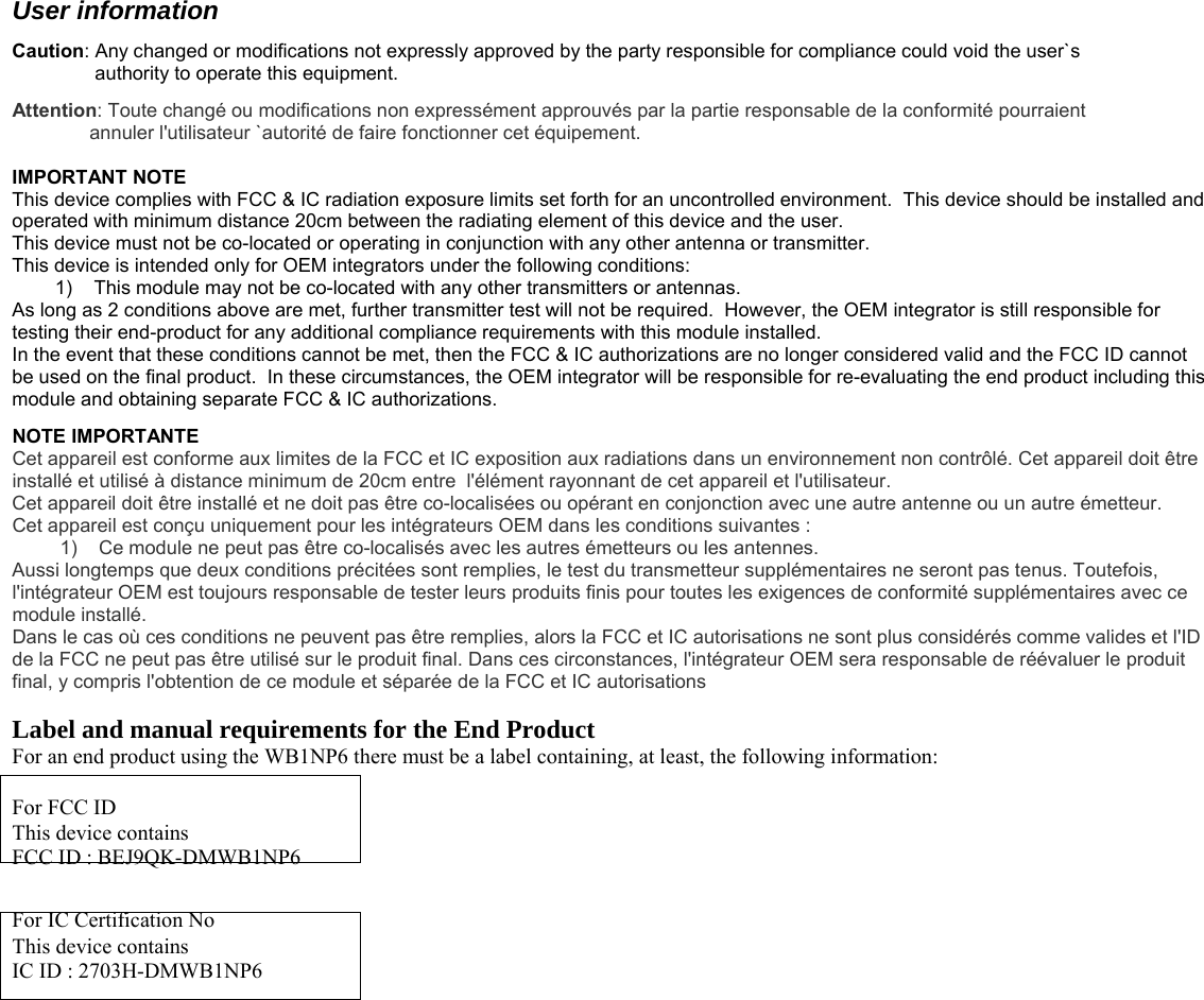
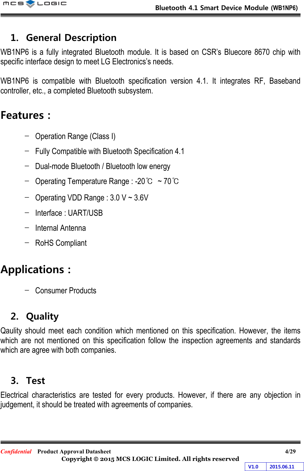
![Bluetooth 4.1 Smart Device Module (WB1NP6) Confidential Product Approval Datasheet 18/29 Copyright 2015 MCS LOGIC Limited. All rights reserved V1.0 2015.06.11 SMT Module Position [TOP VIEW] [BOTTOM VIEW]](https://usermanual.wiki/LG-Electronics-USA/9QK-DMWB1NP6/User-Guide-2659733-Page-11.png)