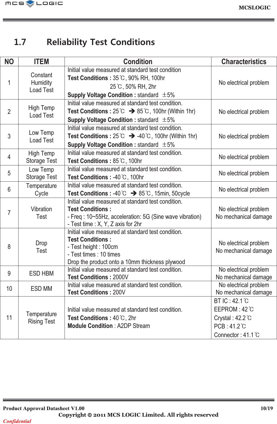
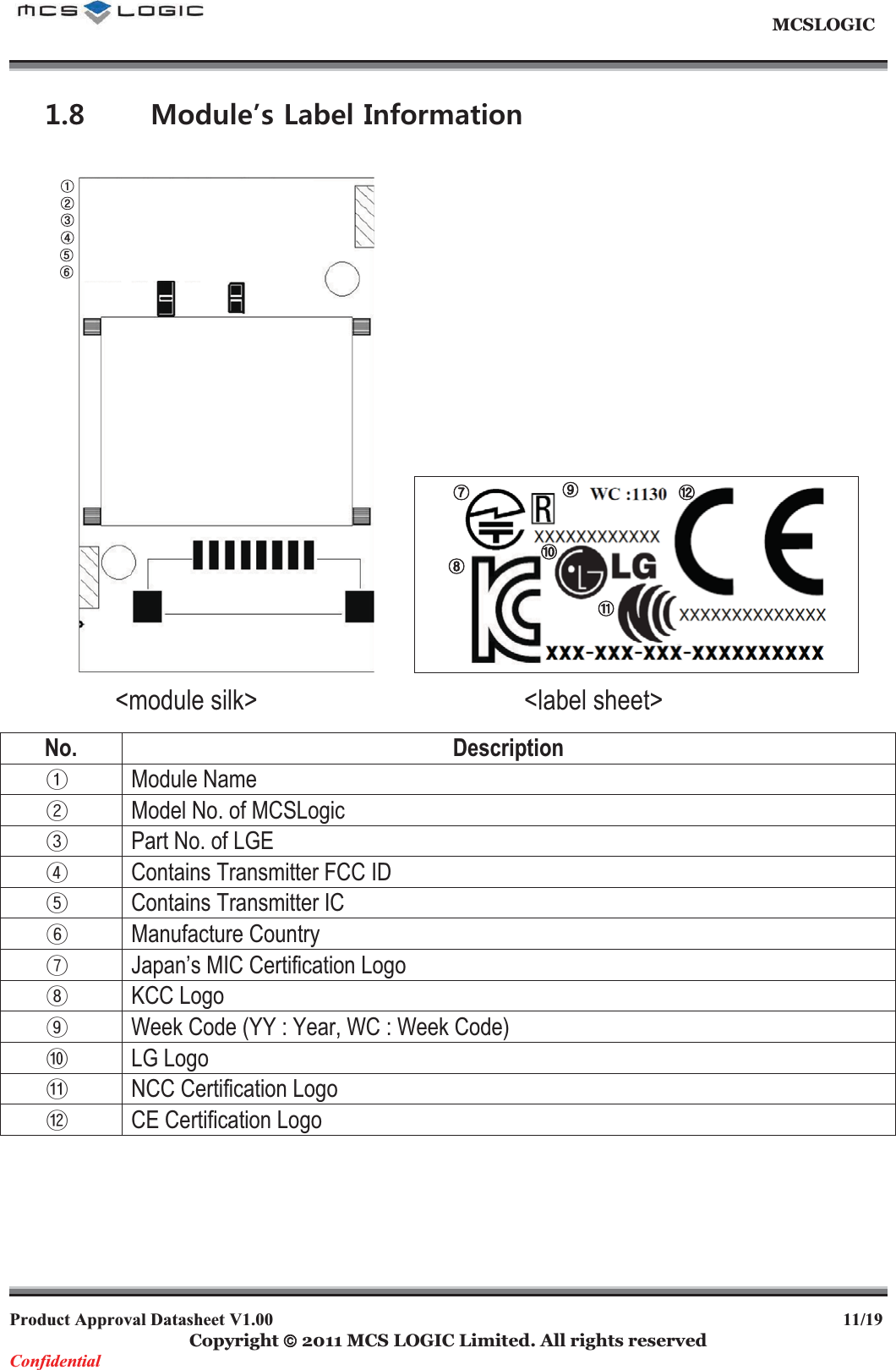
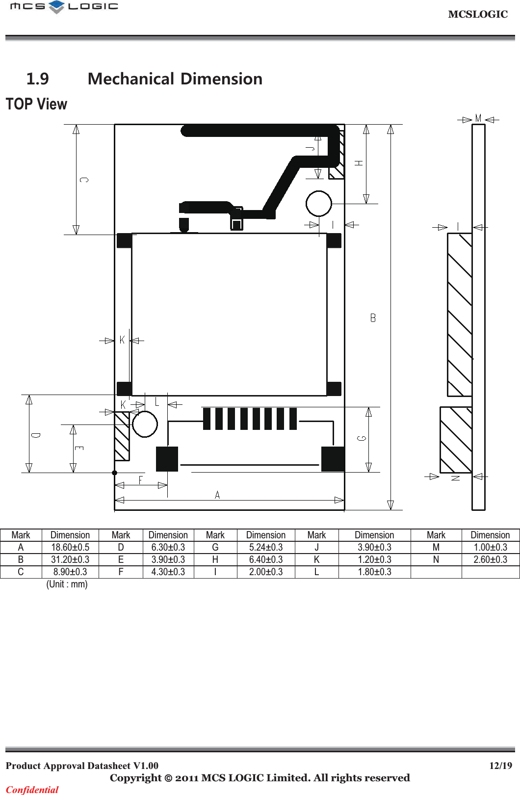
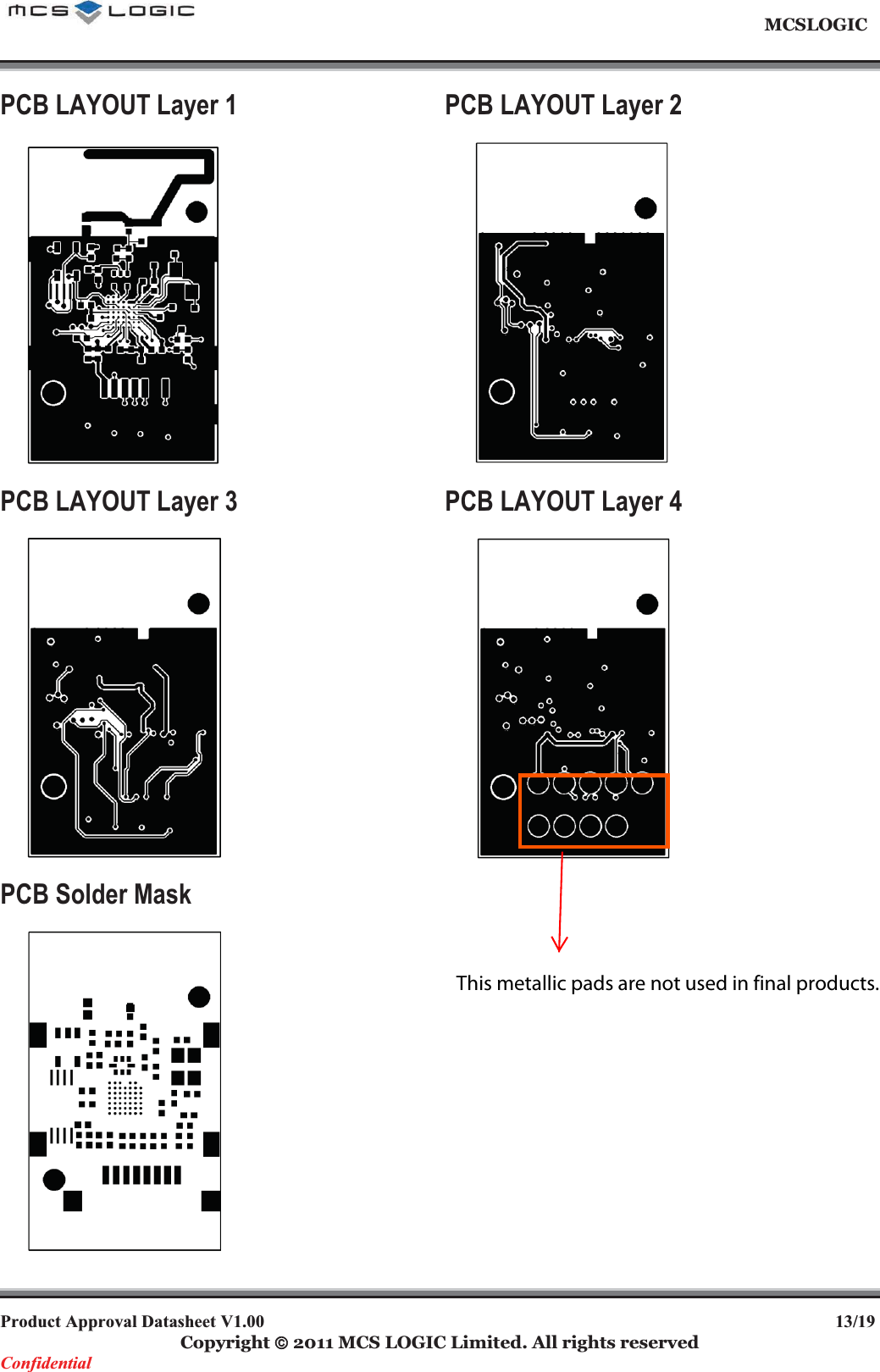
LG Electronics USA 9QK-MB0402C2 Bluetooth Module User Manual operational description and
LG Electronics USA Bluetooth Module operational description and
UserManual.wiki
>
LG Electronics USA
>
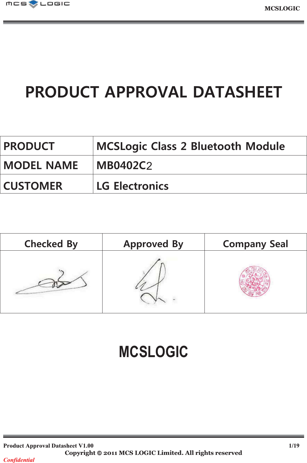
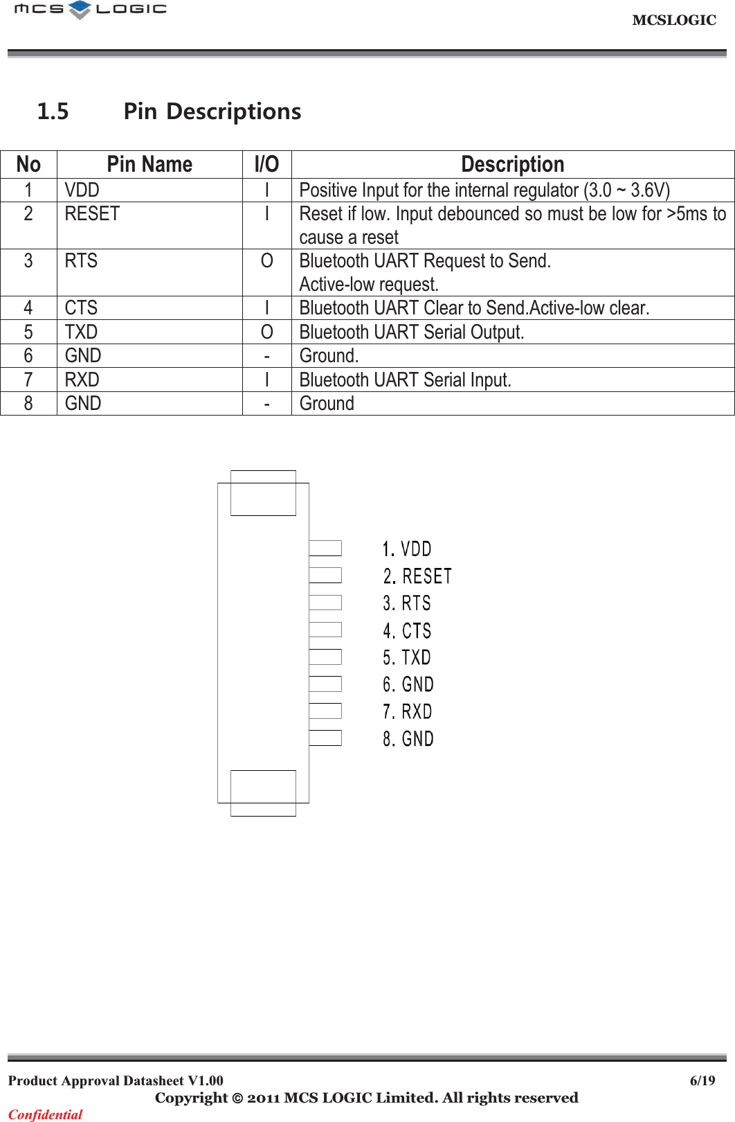
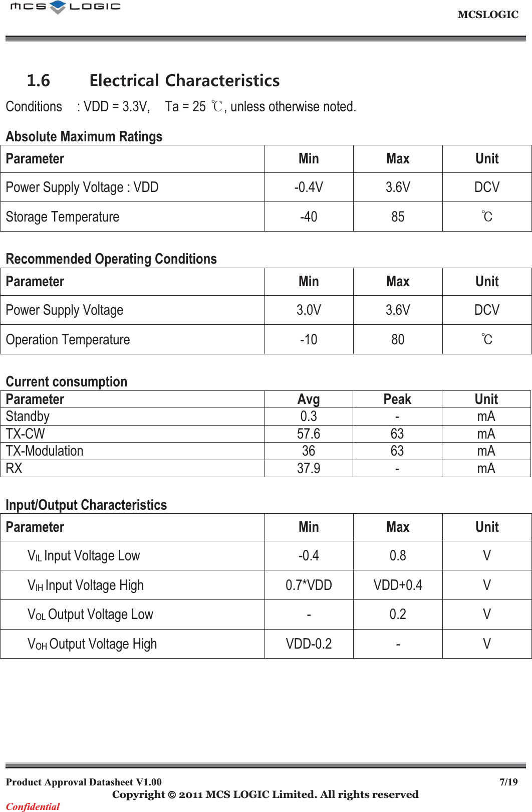
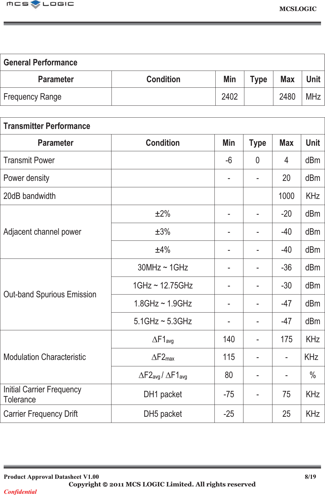
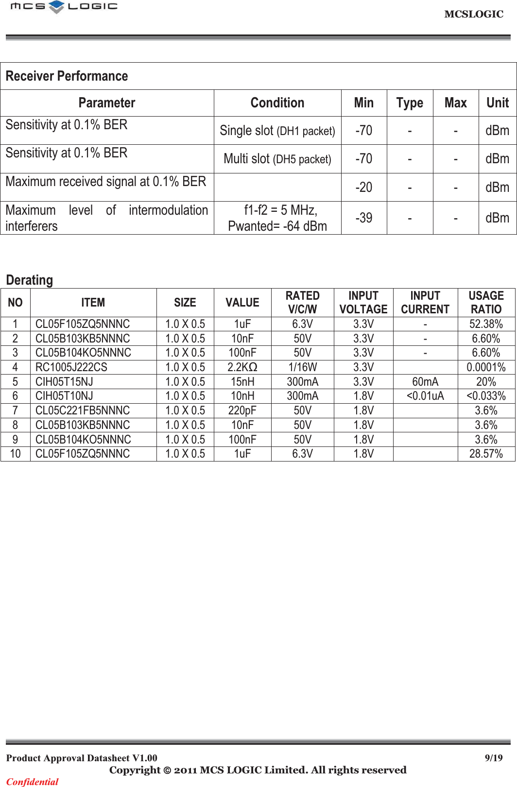
9QK MB0402C2 User Manual
operational description and user manual
Navigation menu
Upload a User Manual
Namespaces
Wiki Guide
HTML
PDF
Info
Views
User Manual
Discussion / Help
Navigation