LG Electronics USA LEO2-A LTE User Equipment User Manual LEO2 Platform Hardware Manual
LG Electronics USA LTE User Equipment LEO2 Platform Hardware Manual
UserManual.wiki
>
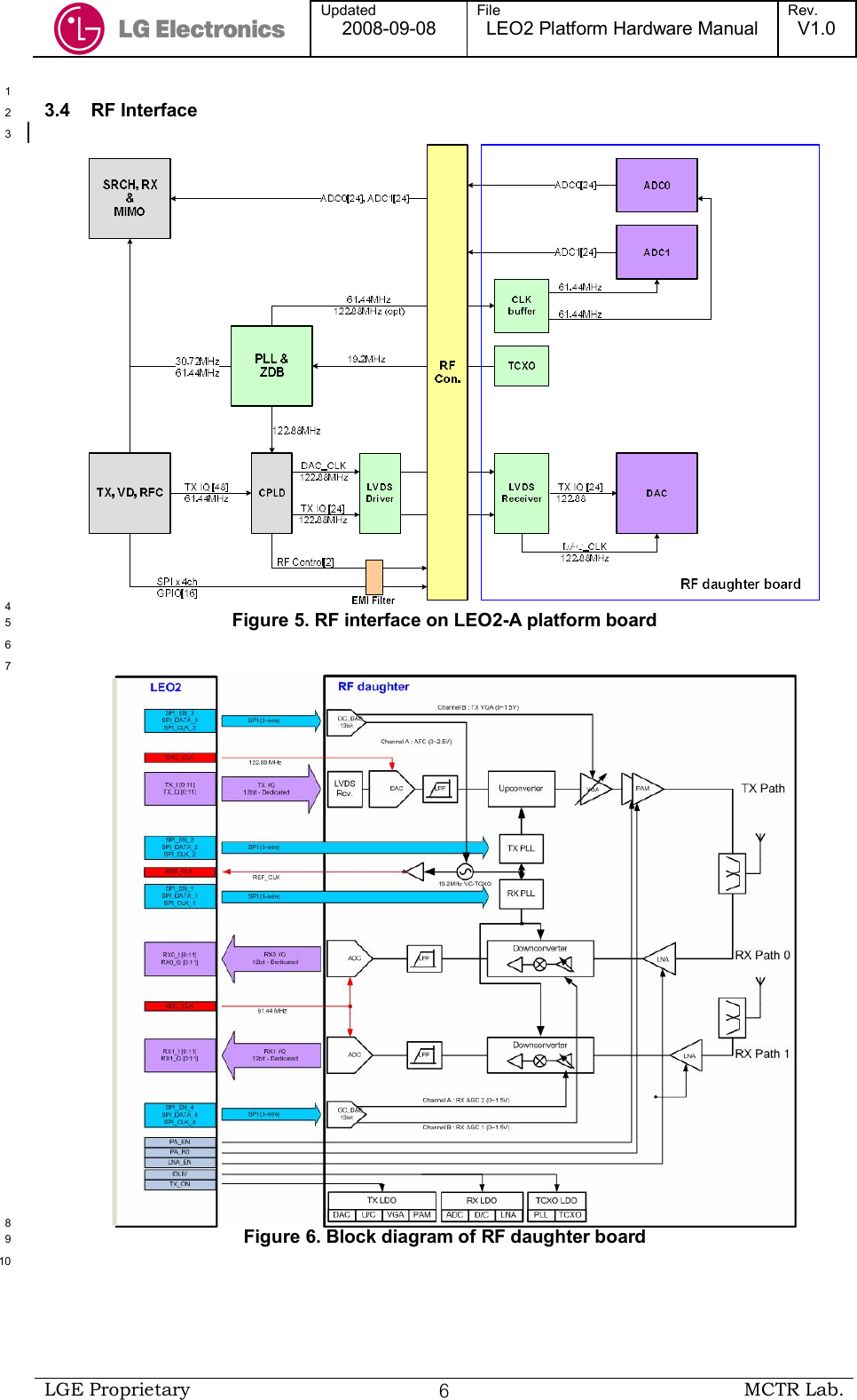
LG Electronics USA
>
LEO2 A User Manual
Users Manual
Navigation menu
Upload a User Manual
Namespaces
Wiki Guide
HTML
PDF
Info
Views
User Manual
Discussion / Help
Navigation
![Updated 2008-09-08 File LEO2 Platform Hardware Manual Rev. V1.0 LGE Proprietary ii MCTR Lab. 1 2 3 4 5 6 7 8 9 10 11 12 13 14 15 16 17 18 19 20 21 22 23 24 25 26 27 28 29 30 31 32 33 34 35 36 37 38 39 40 41 42 43 44 [Notice] 45 1. The product described in this manual may be modified without prior notice for reliability, 46 functionality or design improvement. 47 2. Information contained in this manual is correct and reliable, but LG shall not be held 48 responsible for damage due to the use of information, product or circuit or infringement of 49 property rights or other rights. 50 3. This manual does not grant users the property rights and other rights of the third party or 51 LG Electronics Inc. 52 4. No part of this manual may be transcribed or duplicated without the written permission of 53 LG Electronics Inc. 54 5. The appearance of the product shown in this manual may slightly differ from that of the 55 actual product. 56](https://usermanual.wiki/LG-Electronics-USA/LEO2-A/User-Guide-1005240-Page-2.png)
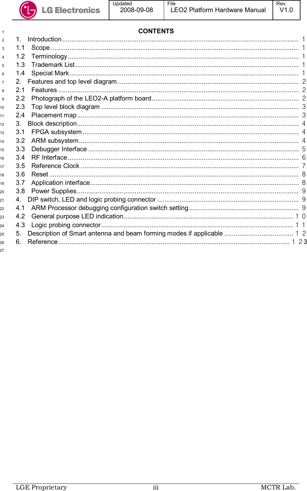
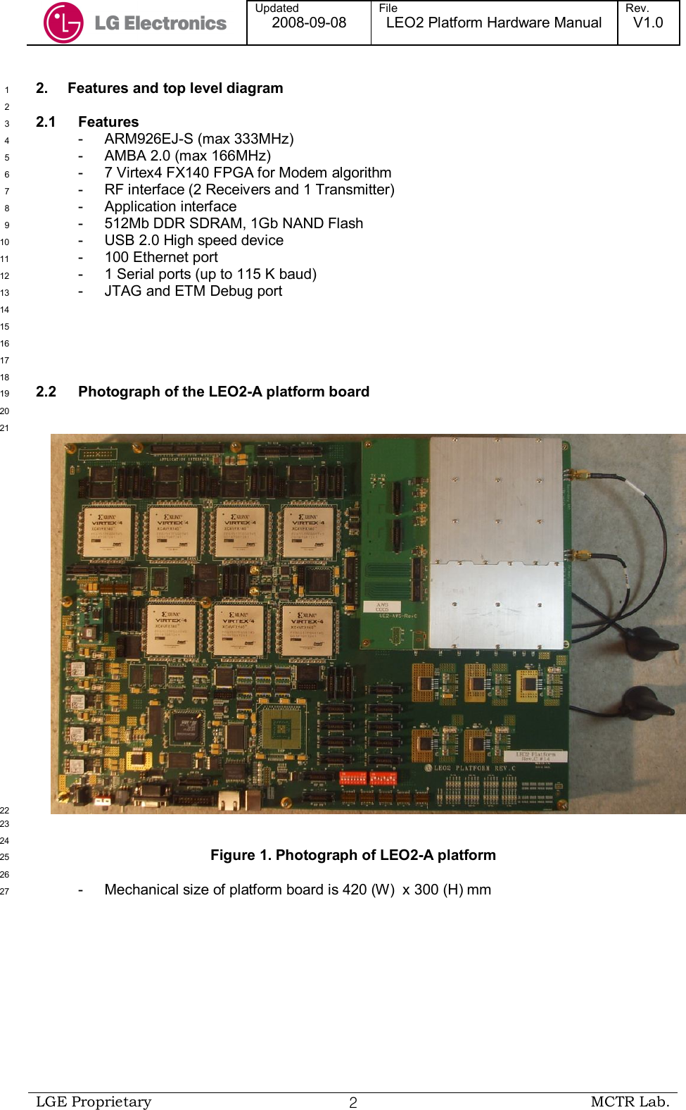
![Updated 2008-09-08 File LEO2 Platform Hardware Manual Rev. V1.0 LGE Proprietary 3 MCTR Lab. 2.3 Top level block diagram 1 2 RX_FRAME_SYNC_NOPT_CTLCH_SYMB[8]OPT _CCH_STB, START, ENDOPT_CCH_IDX[10]RSVD[10]32 Signals54 SignalsCTLCH_SYMB[8]CTLCH_STB, START, ENDCTLCH_IDX[10]OPT_RX_FRAME_SYNC_NRSVD[32]TX_FI LTER_OUT[48]TX_FILTER_IQ_SELRSVD[10]59 SignalsRF_GPIO[16]4ch SPI32 SignalsRX_FRAME_SYNC_NRX_SUB_FRAME_SYNC_NENG_EN[5]ORX_WR, ADDR[10], DATA[32]MIMO_WR_ADDR[10], DATA[32]SC_RD_DATA0[32]SC_RD_DATA1[32]SC_RD_STB, IDX[2]SC_RD_EN, ADDR[11]SC_RD_SYMB_IDX[2]ORX_OPT[100]RSVD[64]310 Signals32 Signals32 Signals51 Signals51 Signals149 Signals149 Signals100 SignalsApplication InterfaceEPI, NAND, USBSDIO, SPI, DIP SW96 SignalsOPT_DCH0_SYMB0[8]OPT_DCH0_SYMB1[8]OPT_DCH0_STB, START, ENDRSVD[13]OPT_DCH1_SYMB0[8]OPT_DCH1_SYMB1[8]OPT_DCH1_STB, START, ENDRSVD[13]DATACH0_SYMB0[8]DATACH0_SYMB1[8]DATACH0_STB, START, ENDRSVD[ 32]DATACH1_SYMB0[8]DATACH1_SYMB1[8]DATACH1_STB, START, ENDRSVD[32]TD0_STARTTD0_IMEM_WE, SEL[3]TD0_IMEM_WADDR[12]TD0_IMEM_WDATA[64]TD0_DB_DONE, DEC_DONEHARQ0_STARTHARQ0_PARAM_STARTRSVD[64]RSVD[100]TX_I[12]TX_Q[12]RSVD[2]26 SignalsRX0_I[ 12], RX0_Q[12]RX1_I[ 12], RX1_Q[12]48 SignalsPLL30.72/61.44/122.88MHzTurboDecoder_CLK64bits mDDRARM926EJ-S64bits mDDRTD1_STARTTD1_IMEM_WE, SEL[3]TD1_IMEM_WADDR[12]TD1_IMEM_WDATA[64]TD1_DB_DONE, DEC_DONEHARQ1_STARTHARQ1_PARAM_STARTRSVD[64]SDRAMUSBUARTETMNANDEthernetSerial FlashJTAGRF Daughter connector 3 Figure 2. Top level block diagram 4 5 6 2.4 Placement map 7 HARQ TP0HARQ TP1TD1 TP0TD1 TP1MIMO TP0MIMO TP1SRCH TP0SRCH TP1TX TP0TX TP1TD0 TP0TD0 TP1HARQ0 TP0HARQ0 TP1RF RX RF TXRESETETHERNETJ1J4J7J10J11J6J3 8 Figure 3. Placement map of the LEO2-A 9](https://usermanual.wiki/LG-Electronics-USA/LEO2-A/User-Guide-1005240-Page-8.png)
![Updated 2008-09-08 File LEO2 Platform Hardware Manual Rev. V1.0 LGE Proprietary 12 MCTR Lab. 6. Reference 1 [1] 2 3 4 Notice 5 6 OEM integrators and installers are instructed that the phrase. This device contains 7 8 Warning: Exposure to Radio Frequency Radiation The radiated output power of this device is far below the FCC radio frequency exposure limits. Nevertheless, the device should be used in such a manner that the potential for human contact during normal operation is minimized. In order to avoid the possibility of exceeding the FCC radio frequency exposure limits, human proximity to the antenna should not be less than 20cm during normal operation. The gain of the antenna for 3GPP-Band4(1710~1755MHz) must not exceed -4 dBi. The antenna(s) used for this transmitter must not be co-located or operating in conjunction with any other antenna or transmitter.](https://usermanual.wiki/LG-Electronics-USA/LEO2-A/User-Guide-1005240-Page-17.png)