LG Electronics USA LGAJ10 GSM/WCDMA/LTE Telematics NAD module User Manual TM01LA N Rev03
LG Electronics USA GSM/WCDMA/LTE Telematics NAD module TM01LA N Rev03
UserManual.wiki
>
LG Electronics USA
>
LGAJ10 User Manual
Users Manual
Navigation menu
Upload a User Manual
Namespaces
Wiki Guide
HTML
PDF
Info
Views
User Manual
Discussion / Help
Navigation

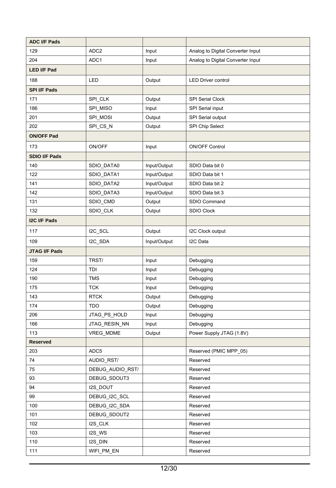
![8/30 [TOP View] [Side view] [TOP View] 1.4.3 Footprint](https://usermanual.wiki/LG-Electronics-USA/LGAJ10/User-Guide-2633897-Page-8.png)
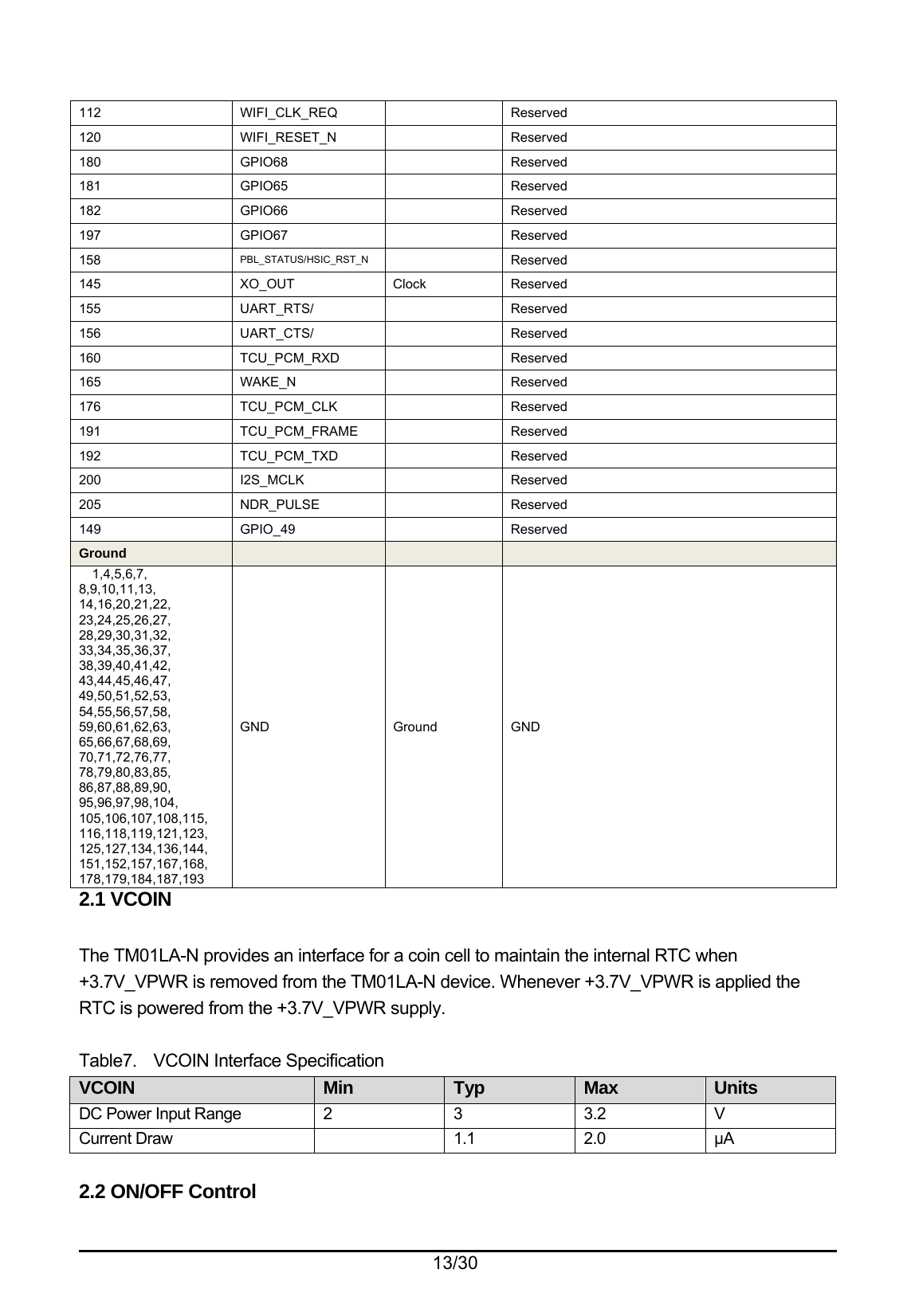
![9/30 [TOP View] 1.5 PCB information 1.5.1 PCB Stack up Layer Meterial DK PSR 0.025 1 Copper 0.035 Pre-Preg 0.060 3.98 2 Copper 0.025 Pre-Preg 0.060 3.98 3 Copper 0.025 Pre-Preg 0.060 3.98 4 Copper 0.025 Pre-Preg 0.110 4.15 5 Copper 0.015 0.75mm(R0.2) 0.85mm(R0.2) 0.95mm](https://usermanual.wiki/LG-Electronics-USA/LGAJ10/User-Guide-2633897-Page-9.png)