LG Electronics USA LGAJ10 GSM/WCDMA/LTE Telematics NAD module User Manual TM01LA N Rev03
LG Electronics USA GSM/WCDMA/LTE Telematics NAD module TM01LA N Rev03
Users Manual

Technical Specification (TM01LA-N)

2/30
History
Ver. Date Contents Written
by
Checked
by
Approved
by Note

3/30
Contents
1. Product Introduction ...................................................................................................... 5
1.1 Block Diagram ...................................................................................................... 5
1.2 Environmental Specifications ............................................................................... 6
1.3 Electrical Specifications ....................................................................................... 6
1.3.1 Absolute Maximum and ESD Ratings ........................................................... 6
1.3.2 Current Consumption .................................................................................... 7
1.4 Mechanical Specifications .................................................................................. 7
1.4.1 Physical Dimensions and Connection Interface ............................................ 7
1.4.2 Mechanical Drawing ...................................................................................... 7
1.4.3 Footprint ........................................................................................................ 7
1.5 PCB information ............................................................................................... 8
1.5.1 PCB Stack up ................................................................................................ 8
1.5.2 PCB VIA Stack up ......................................................................................... 8
2. Pin Definitions ............................................................................................................... 9
2.1 VCOIN ................................................................................................................ 12
2.2 ON/OFF Control ................................................................................................. 12
2.2.1 ON/OFF Timing ........................................................................................... 12
2.2.2 Deep Sleep .................................................................................................. 13
2.2.3 Sequence to Enter Deep Sleep Mode ......................................................... 15
2.3 USB .................................................................................................................... 15
2.4 UART ................................................................................................................. 15
2.5 UIM Interface ..................................................................................................... 16
2.6 General Purpose IO ........................................................................................... 16
2.7 Secure Digital IO ................................................................................................ 16
2.8 I2C Interface ..................................................................................................... 17
2.9 RESET ............................................................................................................... 17
2.10 ADC .................................................................................................................. 18
2.11 LED driver ....................................................................................................... 19
2.13 SPI Interface .................................................................................................. 19
2.14 HSIC Interface ................................................................................................ 20
2.15 JTAG Interface ............................................................................................... 20
3 RF Specification ......................................................................................................... 21
3.1. WCDMA B1, B2, B4, B5 Specification .............................................................. 21
3.2. LTE B1, B2, B4, B5, B7, B12 Specification………………………………………..22
3.3. GSM 850/900/1800/1900 Specification ............................................................ 24

4/30
4. GNSS ........................................................................................................................ 25
4.1 GNSS Characteristics ........................................................................................ 26
4.2 GNSS Antenna Interface .................................................................................... 26
4.3 Active antenna Powering the External LNA ....................................................... 26
5/30
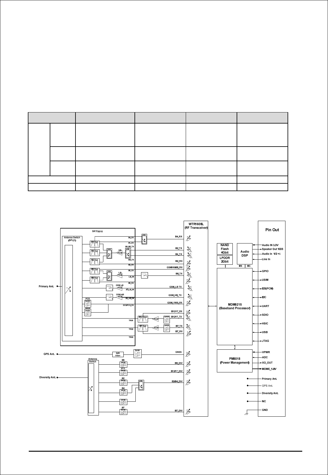
1. Product Introuction
The TM01LA-N are designed for the automotive industry. They support LTE, WCDMA and
GSM air Interface standards. They also have Global Navigation satellite system (GNSS)
capabilities including GPS and GLONASS.
The TM01LA-N are based on the Qualcomm MDM9215 wireless chipsets and support the
following bands.
Table 1. Supported Band
Region NA TML1-E TML1-C Comments
Band
LTE B2/B4/B5/B7/
B12/B17
WCDM
A B2/B4/B5
GSM GSM850/PCS1900
GNSS O
Voice O
1.1 Block Diagram
Figure 1.1. TML1-N Block diagram
6/30
1.2 Environmental Specifications
The environmental specification for operating and storage of the TM01LA-N are defined in the
the table below.
Table 2. Environmental Specifications
Parameter Temperature Range
Operating Temperature -40℃ to 85℃
Storage Temperature -40℃ to +90℃
Humidity 95% or less
1.3 Electrical Specifications
This section provides details for some of the key electrical specifications of the TM01LA-N
embedded modules.
1.3.1 Absolute Maximum Rating and ESD Ratings
This section defines the Absolute Maximum and Electrostatic Discharge (ESD) Ratings of
the TM01LA-N embedded modules.
Warning: If these parameters are exceeded, even momentarily, damage may occur to the
device.
Table 3. Absolute Maximum Ratings
Parameter Min Max Units
+3.7V_VPWR Power Supply Input - tbd V
VIN Voltage on any digital input or output pin - VREG_MDME+0.5 V
Maximum Voltage applied to antenna interface pins
VANT Primary Antenna tbd V
Diversity Antenna tbd V
GNSS Antenna tbd V
ESD Ratings
ESD1
Primary, Diversity and GNSS antenna
pads - Contact
tbd kV
All other signal pads - Contact tbd kV
1 The ESD Simulator configured with 330pF, 1000Ω.
Caution: The TM01LA-N embedded modules are sensitive to Electrostatic Discharge. ESD
countermeasures and handling methods must be used when handling the TM01LA-N
devices.
7/30
1.3.2 Current Consumption
Table 4. TM01LA-N Current Consumption (TBD)
Mode Parameter Typical Max Units
WCDMA
Band 2, Max TX Output Power
mA
Band 4, Max TX Output Power
Band 5, Max TX Output Power
Band 5, Max TX Output Power
LTE
Band2, Max TX Output /Full RB
mA
Band4, Max TX Output /Full RB
Band5, Max TX Output /Full RB
Band7, Max TX Output /Full RB
Band12, Max TX Output /Full RB
Band17, Max TX Output /Full RB
GSM 850/900MHz PCL5
mA
1800/1900MHz PCL0
WCDMA Idle, Registered mA
LTE Idle, Registered mA
GSM Idle, Registered mA
WCDMA Sleep Mode, Average Current mA
LTE Sleep Mode, Average Current mA
GSM Sleep Mode, Average Current mA
1.4 Mechanical Specifications
1.4.1 Physical Dimensions and Connection Interface
The TM01LA-N embedded modules are a Land Grid Array (LGA) form factor device. The
device does not have a System or RF connectors. All electrical and mechanical connections
are made via the 206 pad TM01LA-N on the underside of the PCB.
Table5. TM01LA-N Embedded Module Dimensions
Parameter Nominal Max Units
Overall Dimension 35 x 35 35.35 x 35.35 mm
Overall Module Height 3.5 3.85 mm
PCB Thickness 1.0 1.1 mm
Flatness Specification 0.1 mm
Weight tbd g
1.4.2 Mechanical Drawing
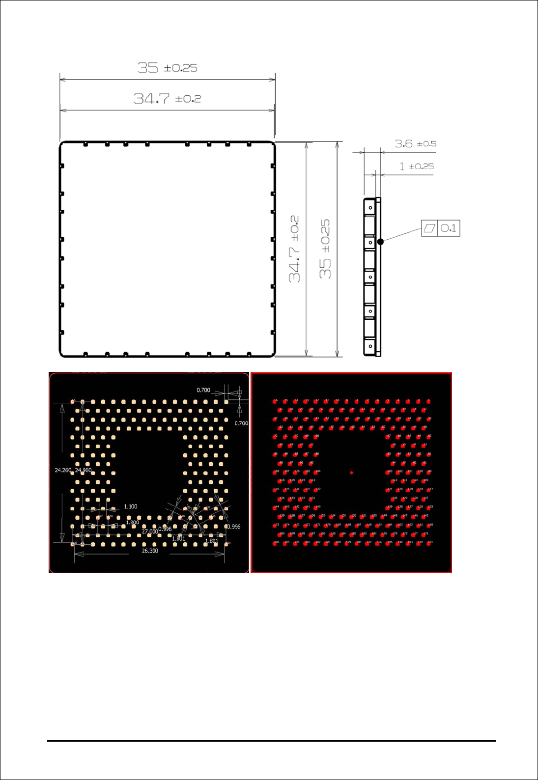
8/30
[TOP View] [Side view]
[TOP View]
1.4.3 Footprint
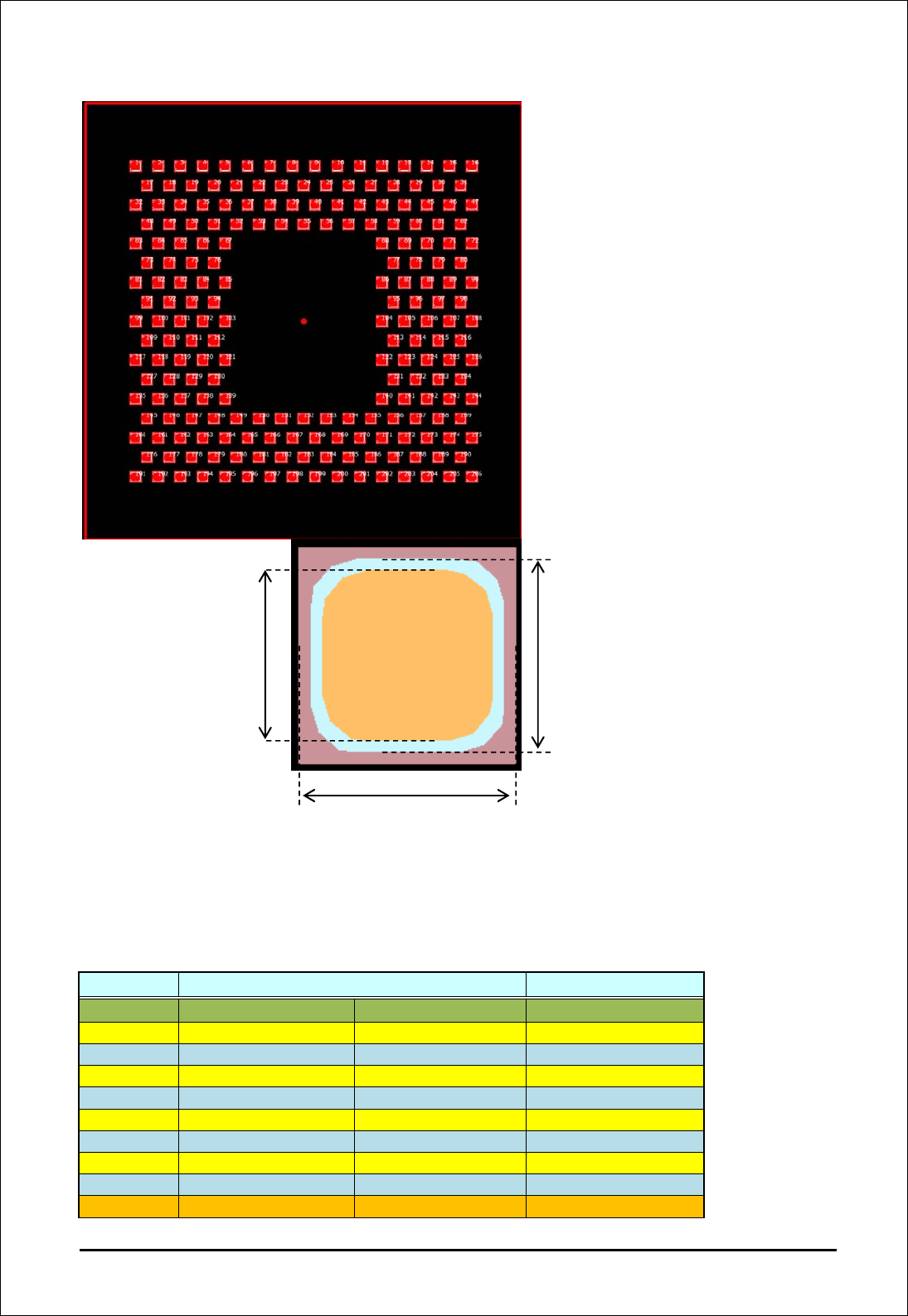
9/30
[TOP View]
1.5 PCB information
1.5.1 PCB Stack up
Layer Meterial DK
PSR 0.025
1 Copper 0.035
Pre-Preg 0.060 3.98
2 Copper 0.025
Pre-Preg 0.060 3.98
3 Copper 0.025
Pre-Preg 0.060 3.98
4 Copper 0.025
Pre-Preg 0.110 4.15
5 Copper 0.015
0.75mm
(
R0.2
)
0.85mm
(
R0.2
)
0.95mm
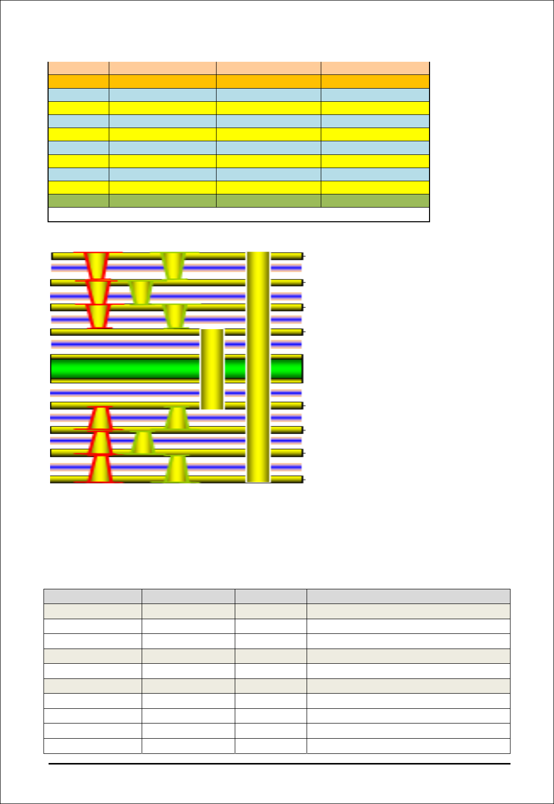
10/30
Core 0.100 4.41
6 Copper 0.015
Pre-Preg 0.110 4.15
7 Copper 0.025
Pre-Preg 0.060 3.98
8 Copper 0.025
Pre-Preg 0.060 3.98
9 Copper 0.025
Pre-Preg 0.060 3.98
10 Copper 0.035
PSR 0.025
0.980
1.5.2 PCB via structure
2. Pin Definitions
Pin No. Name Direction Description
RF Antenna Pads
12 ANT_MAIN Input/Output
15 ANT_DIVERSITY Input
GNSS Antenna Pad
126 ANT_GNSS Input
Power Supply Pads
81,82,91,92 +3.7V_VPWR Input Power Supply Input
114 VREG_MDME Output Voltage Reference Output (1.8V)
84 VDD_AUDIO_3.3V Input Audio codec power supply (typ 3.3V)
135 VCOIN_3.3V Input Coin Battery Input
11/30
USB Pads
185 USB_VBUS Input USB Power Supply
198 USB_D+ Input/Output Differential data interface positive
183 USB_D- Input/Output Differential data interface negative
199 USB_ID Input USB ID
UART Pads
153 UART_RXD Output Receive Data (UART1)
169 UART_TXD Input Transmit Data (UART1)
154 UART2_RXD Output UART2 Receive Data
170 UART2_TXD Input UART2 Transmit Data
UIM Pads
146 VREG_USIM Output Supply output for an UIM card
177 UIM_DET Input Detection of an external UIM card
162 UIM_RESET Output Reset output to an external UIM card
161 UIM_DATA Input/Output Data connection with an external UIM card
163 UIM_CLK Output Clock output to an external UIM card
GPIO I/F Pads
172 GPIO1 Pull-Down Available-GPIO
128 GPIO2 Pull-Down Available-GPIO
150 GPIO3 Pull-Down Available-GPIO
164 GPIO4 Pull-Down Available-GPIO
139 GPIO5 Pull-Down Available-GPIO
189 GPIO6 Pull-Down Available-GPIO
137 GPIO7 Pull-Down Available-GPIO
138 GPIO8 Pull-Down Available-GPIO
148 GPIO9 Pull-Down Available-GPIO
130 GPIO10 Pull-Down Available-GPIO
Analog Audio I/F Pads
2 AUDIO_INP1 Input Microphone 1 input positive
3 AUDIO_INN1 Input Microphone 1 input negative
17 AUDIO_INP2 Input Microphone 2 input positive
18 AUDIO_INN2 Input Microphone 2 input negative
19 AUDIO_LINE_IN Input Audio LINE_IN input
48 SPK_OUT3 Output Speaker 3 output
64 SPK_OUT1 Output Speaker 1 output
73 SPK_OUT2 Output Speaker 2 output
HSIC I/F Pads
195 HSIC_STB Input/Output HSIC Strobe signal
194 HSIC_DATA Input/Output HSIC data signal
196 HSIC_CAL Input/Output HSIC calibration pad
Reset Pads
147 RESET_N Input External H/W Reset Input
133 RESOUT_N Output MDM Reset Output
12/30
ADC I/F Pads
129 ADC2 Input Analog to Digital Converter Input
204 ADC1 Input Analog to Digital Converter Input
LED I/F Pad
188 LED Output LED Driver control
SPI I/F Pads
171 SPI_CLK Output SPI Serial Clock
186 SPI_MISO Input SPI Serial input
201 SPI_MOSI Output SPI Serial output
202 SPI_CS_N Output SPI Chip Select
ON/OFF Pad
173 ON/OFF Input ON/OFF Control
SDIO I/F Pads
140 SDIO_DATA0 Input/Output SDIO Data bit 0
122 SDIO_DATA1 Input/Output SDIO Data bit 1
141 SDIO_DATA2 Input/Output SDIO Data bit 2
142 SDIO_DATA3 Input/Output SDIO Data bit 3
131 SDIO_CMD Output SDIO Command
132 SDIO_CLK Output SDIO Clock
I2C I/F Pads
117 I2C_SCL Output I2C Clock output
109 I2C_SDA Input/Output I2C Data
JTAG I/F Pads
159 TRST/ Input Debugging
124 TDI Input Debugging
190 TMS Input Debugging
175 TCK Input Debugging
143 RTCK Output Debugging
174 TDO Output Debugging
206 JTAG_PS_HOLD Input Debugging
166 JTAG_RESIN_NN Input Debugging
113 VREG_MDME Output Power Supply JTAG (1.8V)
Reserved
203 ADC5 Reserved (PMIC MPP_05)
74 AUDIO_RST/ Reserved
75 DEBUG_AUDIO_RST/ Reserved
93 DEBUG_SDOUT3 Reserved
94 I2S_DOUT Reserved
99 DEBUG_I2C_SCL Reserved
100 DEBUG_I2C_SDA Reserved
101 DEBUG_SDOUT2 Reserved
102 I2S_CLK Reserved
103 I2S_WS Reserved
110 I2S_DIN Reserved
111 WIFI_PM_EN Reserved
13/30
112 WIFI_CLK_REQ Reserved
120 WIFI_RESET_N Reserved
180 GPIO68 Reserved
181 GPIO65 Reserved
182 GPIO66 Reserved
197 GPIO67 Reserved
158 PBL_STATUS/HSIC_RST_N Reserved
145 XO_OUT Clock Reserved
155 UART_RTS/ Reserved
156 UART_CTS/ Reserved
160 TCU_PCM_RXD Reserved
165 WAKE_N Reserved
176 TCU_PCM_CLK Reserved
191 TCU_PCM_FRAME Reserved
192 TCU_PCM_TXD Reserved
200 I2S_MCLK Reserved
205 NDR_PULSE Reserved
149 GPIO_49 Reserved
Ground
1,4,5,6,7,
8,9,10,11,13,
14,16,20,21,22,
23,24,25,26,27,
28,29,30,31,32,
33,34,35,36,37,
38,39,40,41,42,
43,44,45,46,47,
49,50,51,52,53,
54,55,56,57,58,
59,60,61,62,63,
65,66,67,68,69,
70,71,72,76,77,
78,79,80,83,85,
86,87,88,89,90,
95,96,97,98,104,
105,106,107,108,115,
116,118,119,121,123,
125,127,134,136,144,
151,152,157,167,168,
178,179,184,187,193
GND Ground GND
2.1 VCOIN
The TM01LA-N provides an interface for a coin cell to maintain the internal RTC when
+3.7V_VPWR is removed from the TM01LA-N device. Whenever +3.7V_VPWR is applied the
RTC is powered from the +3.7V_VPWR supply.
Table7. VCOIN Interface Specification
VCOIN Min Typ Max Units
DC Power Input Range 2 3 3.2 V
Current Draw 1.1 2.0 μA
2.2 ON/OFF Control
14/30
The ON/OFF signal is internally pulled up to an internal 1.8V reference voltage. An open drain
transistor should be connected to this pin to generate a low pulse. This pin should not be driven
high external to the TM01LA-N embedded module.
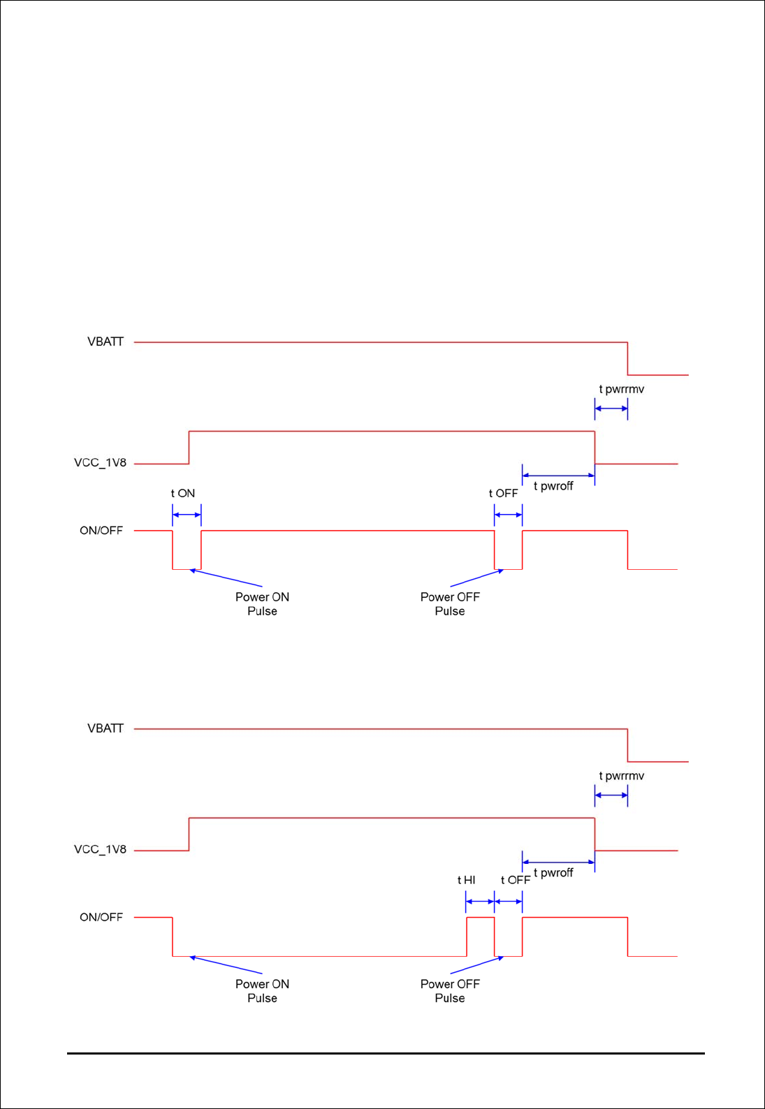
2.2.1 ON/OFF Timing (TBD)
The ON/OFF pin is a low pulse toggle control. The first pulse powers the TM01LA-N ON, a
second pulse instructs the TM01LA-N to begin the Shutdown process.
The diagram below illustrates the recommended application implementation for ON/OFF
control.
The diagram below illustrates an alternate application implementation that holds ON/OFF low
during operation.
15/30
Table8. Power-ON Sequence Symbol Definitions (TBD)
Symbol Parameter Boot Min Typ Max
t ON Turn ON Pulse duration TBD TBD
t OFF Turn OFF Pulse duration TBD TBD TBD
t pwroff Time to Power OFF - TBD
t pwrrmv Time +3.7V_VPWR must be
maintained after VREG_MDME
goes inactive
TBD
t HI Time required for ON/OFF to be
high prior to OFF pulse.
In process TBD
Complete TBD
T pwroff is the time between when a power OFF pulse is complete and when shutdown is
completed by the TM01LA-N devices. This duration is network and device dependent, i.e. in a
CDMA network a power down registration is initiated by the TM01LA-N device, when the
acknowledgement is received from the network power OFF completes.
Detection of power down can be accomplished by monitoring for one of the following:
+WIND: 10 output on the AT Command interface
USB ports are de-enumerated
The application must wait for a power down to be detected prior to removing power from the
TM01LA-N device. If a timeout is required, it is recommended to be in excess of 30s prior to
removing power from the TM01LA-N device.
2.2.2 Deep Sleep
The TM01LA-N embedded modules support a low power mode in which the device is
registered on the LTE/GSM/WCDMA network and sleeps in between wake intervals where it
listens for pages.
The following table lists the parameter that defines the wake interval period for the various
devices.
Table9. Period of Wake Intervals
16/30
Device Network Standard Parameter
TM01LA-N GSM DRX
WCDMA DRX
LTE DRX
The DRX cycle index values are broadcast by the wireless network on which the TM01LA-N
embedded module is registered.
While in Deep Sleep mode the functions of the TM01LA-N are limited as defined in the
following table.
Table10. Deep Sleep Function Availability
Function Availability Conditions
Paging
GNSS GNSS is powered down
Time measurement
USB USB_VBUS is not applied
UART
Digital IO Digital IO pins maintained last state
Events that cause the TM01LA-N to wake-up from Deep Sleep mode include:
Incoming call
Expiration of an internal timer in the TM01LA-N
USB_VBUS is applied to the TM01LA-N
WAKE_N is asserted (low)
UART1 DTR is asserted (high) if UART1 DTR has been enabled as a sleep control
(AT+W32K=1,1) and AT Command Service is mapped to UART1
GNSS location fix request is initiated from an Embedded Application
2.2.3 Sequence to Enter Deep Sleep Mode
The following list defines the sequence needed by the application to allow the TM01LA-N to
enter Deep Sleep mode:
1. TM01LA-N has registered on the WWAN network (or callbox), and is not in a call.
2. End GNSS Tracking session.
3. Turn off GNSS Antenna bias.
4. Confirm WAKE_N is not held low (pulled-up in TM01LA-N).
5. Issue AT command to request AR device to enter deep sleep (AT+W32K=1,x).
6. If AT+W32K=1,1 is used, DTR must also be de-asserted to allow sleep.
7. Ensure UARTs are in the inactive state.
8. Remove VBUS from being applied to the AR device.
2.3 USB
17/30
The TM01LA-N has a High Speed USB2.0 compliant, peripheral only interface. The TM01LA-N
don’t support OTG.
The TM01LA-N will not be damaged if a valid USB_VBUS is supplied while the main DC power
is not supplied.
Table10. USB Characteristics
USB Value Units
USB_VBUS Voltage range 2.0 – 5.25 V
Maximum Current draw 1 1 mA
Maximum Input Capacitance
(Min ESR = 50 mΩ)
10 μF
1 With the TM01LA-N device powered ON.
2.4 UART
The TM01LA-N has two UART interfaces. The primary UART is an 4-wire electrical interface
and the secondary UART is a 2-wire electrical interface.
Table11. UART Interface PADs
Pin No. Name Direction Description
153 UART_RXD Output Receive Data (UART1)
169 UART_TXD Input Transmit Data (UART1)
154 UART2_RXD Output Receive Data (UART2)
170 UART2_TXD Input Transmit Data (UART2)
155 UART_RTS/ Output Request To Send(UART1)
156 UART_CTS/ Input Clear To Send(UART1)
2.5 UIM Interface
The UIM interface of the TM01LA-N supports a USIM for LTE, WCDMA and GSM.
Table13. UIM Interface PADs
Pin No. Name Direction Description
146 VREG_USIM Output Supply output for an UIM card
177 UIM_DET Input Detection of an external UIM card
162 UIM_RESET Output Reset output to an external UIM card
161 UIM_DATA Input/Output Data connection with an external UIM card
163 UIM_CLK Output Clock output to an external UIM card
2.6 General Purpose IO
18/30
The TM01LA-N defines 10 GPIOs for customer use.
Table14. GPIO Inferface PADs
Pin No. Name Direction Description
172 GPIO1 Pull-Down Available-GPIO
128 GPIO2 Pull-Down Available-GPIO
150 GPIO3 Pull-Down Available-GPIO
164 GPIO4 Pull-Down Available-GPIO
139 GPIO5 Pull-Down Available-GPIO
189 GPIO6 Pull-Down Available-GPIO
137 GPIO7 Pull-Down Available-GPIO
138 GPIO8 Pull-Down Available-GPIO
148 GPIO9 Pull-Down Available-GPIO
130 GPIO10 Pull-Down Available-GPIO
2.7 Secure Digital IO
The TM01LA-N defines a 1.8V SDIO interface for future use.
Table15. SDIO Inferface PADs
Pin No. Name Direction Description
140 SDIO_DATA0 Input/Output SDIO Data bit 0
122 SDIO_DATA1 Input/Output SDIO Data bit 1
141 SDIO_DATA2 Input/Output SDIO Data bit 2
142 SDIO_DATA3 Input/Output SDIO Data bit 3
131 SDIO_CMD Output SDIO Command
132 SDIO_CLK Output SDIO Clock
2.8 I2C Interface
The TM01LA-N provides an I2C interface.
The I2C signals are open drain outputs with 2.2 kΩ pull-up resistors toVREG_MDME (1.8V)
internal to the TM01LA-N.
Table16. I2C Inferface PADs
Pin No. Name Direction Description
117 I2C_SCL Output I2C Clock output
109 I2C_SDA Input/Output I2C Data
2.9 RESET
19/30
The TM01LA-N provides an interface to allow an external application to RESET the module as
well as an output to indicate the current RESET state or control an external device.
The RESIN_N signal is pulled-up internal to the TM01LA-N. An open collector transistor or
equivalent should be used to Ground the signal when necessary to RESET the module.
Note: Use of the RESIN_N signal to RESET the TM01LA-N could result in memory
corruption if used inappropriately. This signal should only be used if the TM01LA-N has
become unresponsive and it is not possible to perform a power cycle.
Table17. Reset Timing
Symbol Parameter Min Typ Max
Trdet Duration of RESIN_N signal before firmware detects it
(debounce timer)
- tbd
Trlen Duration reset asserted tbd
Trdel Delay between minimum Reset duration and Internal
Reset generated
- tbd
Figure . Illustration of Reset Timing When RESIN_N < Trdel
Figure. Illustration of Reset Timing When RESIN_N Held Low > Trdet+Trdel
2.10 ADC
20/30
The TM01LA-N provides two ADC inputs. The interface information is provided in the tables
below.
Table18. ADC Interface Characteristics
ADC Value Units
ADCx Full-Scale Voltage Level 0.05 ~ 1.75 V
Resolution 15 bit
Sample rate 1.15 (tbd) KHz
Input Impedance >4 MΩ
2.11 LED driver
The TM01LA-N provides an LED driver. The LED driver is a programmable current sink.
Table19. LED Inferface PAD
Pin No. Name Direction Description
188 LED Output LED Driver control
2.12 Audio
The TM01LA-N supports Analog audio interfaces.
The ADC blocks supports Stereo 24-bit Inputs (Differential, Single-ended) and Mono 24-bit
(Line-In).
The DAC blocks supports Stereo 24-bit output (Stereo) and Line output (Single-ended).
Table20. Audio Inferface PADs
Pin No. Name Direction Description
2 AUDIO_INP1 Input Microphone 1 input positive
3 AUDIO_INN1 Input Microphone 1 input negative
17 AUDIO_INP2 Input Microphone 2 input positive
18 AUDIO_INN2 Input Microphone 2 input negative
19 AUDIO_LINE_IN Input Audio LINE_IN input
48 SPK_OUT3 Output Speaker 3 output
64 SPK_OUT1 Output Speaker 1 output
73 SPK_OUT2 Output Speaker 2 output
2.13 SPI Interface
The TM01LA-N embedded module provides one SPI bus (4-wire interface).
SPI bus interface includes:
21/30
A CLK signal
An O signal
An I signal
A CS (Chip Select) signal
The following features are available on the SPI bus :
Master-only mode operation
SPI speed is from 128 kbit/s to 26Mbit/s in master mode operation
4-wire interface
4 to 32 bits data length. (TBD)
Table21. SPI Inferface PADs
Pin No. Name Direction Description
171 SPI_CLK Output SPI Serial Clock
186 SPI_MISO Input SPI Serial input
201 SPI_MOSI Output SPI Serial output
202 SPI_CS_N Output SPI Chip Select
2.14 HSIC Interface
The TM01LA-N embedded module provides one HSIC bus (2-wire interface).
HSIC bus interface includes:
HSIC strobe signal
HSIC data signal
Calibration pad for HSIC port signal
Table22. HSIC Inferface PADs
Pin No. Name Direction Description
195 HSIC_STB Input/Output HSIC Strobe signal
194 HSIC_DATA Input/Output HSIC data signal
196 HSIC_CAL Input/Output HSIC calibration pad
2.15 JTAG Interface
JTAG test points on customer application are recommended for possible failure analysis if
necessary in the future.
Table23. JTAG Inferface PADs
Pin No. Name Direction Description
159 TRST/ Input Debugging
22/30
124 TDI Input Debugging
190 TMS Input Debugging
175 TCK Input Debugging
143 RTCK Output Debugging
174 TDO Output Debugging
206 JTAG_PS_HOLD Input Debugging
166 JTAG_RESIN_NN Input Debugging
113 VREG_MDME Output Power Supply JTAG (1.8V)
3. RF Specification
The specifications for the LTE, GSM and WCDMA interfaces are defined.
TM01LA-N is designed to be compliant with the standard shown in the table below.
Table24. Standards Compliance
Technology Standards
UMTS (WCDMA)
• 3GPP Release 5
• 3GPP Release 6
• 3GPP Release 7
• 3GPP Release 8
LTE • 3GPP Release 8
GSM/GPRS/EDGE • 3GPP Release R99
3.1 WCDMA B1, B2, B4, B5 Specification
3.1.1 WCDMA TX Output Power
The Maximum / Minimum Transmitter Output Power of the TM01LA-N are specified in the
following table.
23/30
Table25.
Band Method (UL CH) Specification
WCDMA Band 2
Power Level
Measure Max and Min Transmit Power of Low
Channel (CH=9263) in WCDMA B2 Mode
Max Power : 21.5~25.5dBm
Min Power : ≤ -50dBm
Measure Max and Min Transmit Power of Middle
Channel (CH=9400) in WCDMA B2 Mode
Max Power : 21.5~25.5dBm
Min Power : ≤ -50dBm
Measure Max and Min Transmit Power of High
Channel (CH=9537) in WCDMA B2 Mode
Max Power : 21.5~25.5dBm
Min Power : ≤ -50dBm
WCDMA Band 4
Power Level
Measure Max and Min Transmit Power of Low
Channel (CH=1313) in WCDMA B4 Mode
Max Power : 21.5~25.5dBm
Min Power : ≤ -50dBm
Measure Max and Min Transmit Power of Middle
Channel (CH=1413) in WCDMA B4 Mode
Max Power : 21.5~25.5dBm
Min Power : ≤ -50dBm
Measure Max and Min Transmit Power of High
Channel (CH=1513) in WCDMA B4 Mode
Max Power : 21.5~25.5dBm
Min Power : ≤ -50dBm
WCDMA Band 5
Power Level
Measure Max and Min Transmit Power of Low
Channel (CH=4133) in WCDMA B5 Mode
Max Power : 21.5~25.5dBm
Min Power : ≤ -50dBm
Measure Max and Min Transmit Power of Middle
Channel (CH=4183) in WCDMA B5 Mode
Max Power : 21.5~25.5dBm
Min Power : ≤ -50dBm
Measure Max and Min Transmit Power of High
Channel (CH=4232) in WCDMA B5 Mode
Max Power : 21.5~25.5dBm
Min Power : ≤ -50dBm
3.1.2 WCDMA RX Sensitivity
The Receiver Sensitivity of the TM01LA-N are specified in the following table.
Table26. Conducted RX (Receive) Sensitivity – UMTS Bands
Item Method (DL CH) Specification
WCDMA Band 2
BER(Bit Error
Rate)
Measure BER of Low Channel (CH=9663) in
WCDMA B2 Mode 0~0.1% @<-104.7dBm
Measure BER of Middle Channel (CH=9800) in
WCDMA B2 Mode 0~0.1% @<-104.7dBm
Measure BER of High Channel (CH=9937) in
WCDMA B2 Mode 0~0.1% @<-104.7dBm
WCDMA Band 4
BER(Bit Error
Rate)
Measure BER of Low Channel (CH=1538) in
WCDMA B4 Mode 0~0.1% @<-106.7dBm
Measure BER of Middle Channel (CH=1675) in
WCDMA B4 Mode 0~0.1% @<-106.7dBm
Measure BER of High Channel (CH=1737) in
WCDMA B4 Mode 0~0.1% @<-106.7dBm
WCDMA Band 5
BER(Bit Error
Rate)
Measure BER of Low Channel (CH=4358) in
WCDMA B5 Mode 0~0.1% @<-104.7dBm
Measure BER of Middle Channel (CH=4400) in
WCDMA B5 Mode 0~0.1% @<-104.7dBm
Measure BER of High Channel (CH=4457) in
WCDMA B5 Mode 0~0.1% @<-104.7dBm
3.2. LTE B1, B2, B4, B5, B7, B12 Specification
3.2.1 LTE TX Output Power
24/30
The Maximum / Minimum Transmitter Output Power of the TM01LA-N are specified in the
following table.
Table27. Conducted TX (Transmit) Max output Power Tolerances – LTE Bands
BAND Method (UL CH) Specification
BAND2
UE Maximum
Output Power
Measure Max and Min Transmit Power of Low
Channel (18650)
Max Power : 20.8~26.2dBm
Min Power : ≤ -39dBm
Measure Max and Min Transmit Power of Mid
Channel (18900)
Max Power : 20.8~26.2dBm
Min Power : ≤ -39dBm
Measure Max and Min Transmit Power of High
Channel (19150)
Max Power : 20.8~26.2dBm
Min Power : ≤ -39dBm
BAND4
UE Maximum
Output Power
Measure Max and Min and Min Transmit Power of
Low Channel (20000)
Max Power : 20.8~26.2dBm
Min Power : ≤ -39dBm
Measure Max and Min Transmit Power of Mid
Channel (20175)
Max Power : 20.8~26.2dBm
Min Power : ≤ -39dBm
Measure Max and Min Transmit Power of High
Channel (20350)
Max Power : 20.8~26.2dBm
Min Power : ≤ -39dBm
BAND5
UE Maximum
Output Power
Measure Max and Min and Min Transmit Power of
Low Channel (20450)
Max Power : 20.8~26.2dBm
Min Power : ≤ -39dBm
Measure Max and Min Transmit Power of Mid
Channel (20525)
Max Power : 20.8~26.2dBm
Min Power : ≤ -39dBm
Measure Max and Min Transmit Power of High
Channel (20600)
Max Power : 20.8~26.2dBm
Min Power : ≤ -39dBm
BAND7
UE Maximum
Output Power
Measure Max and Min and Min Transmit Power of
Low Channel (20800)
Max Power : 20.8~26.2dBm
Min Power : ≤ -39dBm
Measure Max and Min Transmit Power of Mid
Channel (21100)
Max Power : 20.8~26.2dBm
Min Power : ≤ -39dBm
Measure Max and Min Transmit Power of High
Channel (21400)
Max Power : 20.8~26.2dBm
Min Power : ≤ -39dBm
BAND12
UE Maximum
Output Power
Measure Max and Min and Min Transmit Power of
Low Channel (23060)
Max Power : 20.8~26.2dBm
Min Power : ≤ -39dBm
Measure Max and Min Transmit Power of Mid
Channel (23095)
Max Power : 20.8~26.2dBm
Min Power : ≤ -39dBm
Measure Max and Min Transmit Power of High
Channel (23130)
Max Power : 20.8~26.2dBm
Min Power : ≤ -39dBm
BAND17
UE Maximum
Output Power
Measure Max and Min and Min Transmit Power of
Low Channel (23735)
Max Power : 20.8~26.2dBm
Min Power : ≤ -39dBm
Measure Max and Min Transmit Power of Mid
Channel (23790)
Max Power : 20.8~26.2dBm
Min Power : ≤ -39dBm
Measure Max and Min Transmit Power of High
Channel (23845)
Max Power : 20.8~26.2dBm
Min Power : ≤ -39dBm
3.2.2 LTE RX Sensitivity
The Receiver Sensitivity of the TM01LA-N are specified in the following table.
Table28. Conducted RX (Receive) Sensitivity – LTE Bands
BAND Method (DL CH) Specification
BAND2
Reference Measure BLER of Low Channel (650) in Band1 sensitivity : ≤-95
BLER : ≤ 5%
25/30
sensitivity
level(DUAL) Measure BLER of Mid Channel (900) in Band1 sensitivity : ≤-95
BLER : ≤ 5%
Measure BLER of High Channel (1150) in Band1 sensitivity : ≤-95
BLER : ≤ 5%
BAND 4
Reference
sensitivity
level(DUAL)
Measure BLER of Low Channel (2000) in Band4 sensitivity : ≤-97
BLER : ≤ 5%
Measure BLER of Mid Channel (2175) in Band4 sensitivity : ≤-97
BLER : ≤ 5%
Measure BLER of High Channel (2350) in
Band4
sensitivity : ≤-97
BLER : ≤ 5%
BAND 5
Reference
sensitivity
level(DUAL)
Measure BLER of Low Channel (2450) in Band5 sensitivity : ≤-95
BLER : ≤ 5%
Measure BLER of Mid Channel (2525) in Band5 sensitivity : ≤-95
BLER : ≤ 5%
Measure BLER of High Channel (2600) in
Band5
sensitivity : ≤-95
BLER : ≤ 5%
BAND 7
Reference
sensitivity
level(DUAL)
Measure BLER of Low Channel (2800) in Band7 sensitivity : ≤-95
BLER : ≤ 5%
Measure BLER of Mid Channel (3100) in Band7 sensitivity : ≤-95
BLER : ≤ 5%
Measure BLER of High Channel (3400) in
Band7
sensitivity : ≤-95
BLER : ≤ 5%
BAND 12
Reference
sensitivity
level(DUAL)
Measure BLER of Low Channel (5060) in Band12 sensitivity : ≤-94
BLER : ≤ 5%
Measure BLER of Mid Channel (5095) in Band12 sensitivity : ≤-94
BLER : ≤ 5%
Measure BLER of High Channel (5130) in
Band12
sensitivity : ≤-94
BLER : ≤ 5%
BAND 17
Reference
sensitivity
level(DUAL)
Measure BLER of Low Channel (5735) in Band12 sensitivity : ≤-94
BLER : ≤ 5%
Measure BLER of Mid Channel (5790) in Band12 sensitivity : ≤-94
BLER : ≤ 5%
Measure BLER of High Channel (5845) in
Band12
sensitivity : ≤-94
BLER : ≤ 5%
3.3 GSM 850/900/1800/1900 Specification
3.3.1 GSM TX Output Power
The Maximum Transmitter Output Power of the TM01LA-N are specified in the following table.
Table29. Conducted TX (Transmit) Max output Power Tolerances – GSM/EDGE Bands
Item Method (DL CH) Specification
GSM850
Power Level
Measure Max Transmit Power of Low Channel
(CH=128) in GSM850 Mode Max Power : 31.0~33.5dBm
Measure Max Transmit Power of Middle Channel
(CH=189) in GSM850 Mode Max Power : 31.0~33.5dBm
Measure Max Transmit Power of High Channel
(CH=251) in GSM850 Mode Max Power : 31.0~33.5dBm
EGSM900
Power Level
Measure Max Transmit Power of Low Channel
(CH=975) in EGSM Mode Max Power : 31.0~33.5dBm
Measure Max Transmit Power of Middle Channel
(CH=38) in EGSM Mode Max Power : 31.0~33.5dBm
Measure Max Transmit Power of High Channel
(CH=124) in EGSM Mode Max Power : 31.0~33.5dBm
26/30
DCS1800
Power Level
Measure Max Transmit Power of Low Channel
(CH=512) in DCS1800 Mode Max Power : 28.0~30.5dBm
Measure Max Transmit Power of Middle Channel
(CH=660) in DCS1800 Mode Max Power : 28.0~30.5dBm
Measure Max Transmit Power of High Channel
(CH=885) in DCS1800 Mode Max Power : 28.0~30.5dBm
PCS1900
Power Level
Measure Max Transmit Power of Low Channel
(CH=512) in DCS1900 Mode Max Power : 28.0~30.5dBm
Measure Max Transmit Power of Middle Channel
(CH=660) in DCS1900 Mode Max Power : 28.0~30.5dBm
Measure Max Transmit Power of High Channel
(CH=810) in DCS1900 Mode Max Power : 28.0~30.5dBm
3.3.2 GSM RX Sensitivity
The Receiver Sensitivity of the TM01LA-N are specified in the following table.
Table30. Conducted RX (Receive) Sensitivity – GSM/EDGE Bands
Item Method (DL CH) Specification
GSM850
BER(Bit Error
Rate)
Measure BER of Low Channel (CH=128)
in GSM850 Mode 0~2.439% @<-102dBm
Measure BER of Middle Channel (CH=189)
in GSM850 Mode 0~2.439% @<-102dBm
Measure BER of High Channel (CH=251)
in GSM850 Mode 0~2.439% @<-102dBm
EGSM900
BER(Bit Error
Rate)
Measure BER of Low Channel (CH=975)
in EGSM Mode 0~2.439% @<-102dBm
Measure BER of Middle Channel (CH=38)
in EGSM Mode 0~2.439% @<-102dBm
Measure BER of High Channel (CH=124)
in EGSM Mode 0~2.439% @<-102dBm
DCS1800
BER(Bit Error
Rate)
Measure BER of Low Channel (CH=512)
in DCS1800 Mode 0~2.439% @<-102dBm
Measure BER of Middle Channel (CH=660)
in DCS1800 Mode 0~2.439% @<-102dBm
Measure BER of High Channel (CH=885)
in DCS1800 Mode 0~2.439% @<-102dBm
PCS1900
BER(Bit Error
Rate)
Measure BER of Low Channel (CH=512)
in PCS1900 Mode 0~2.439% @<-102dBm
Measure BER of Middle Channel (CH=660)
in PCS1900 Mode 0~2.439% @<-102dBm
Measure BER of High Channel (CH=810)
in PCS1900 Mode 0~2.439% @<-102dBm
4. GNSS
The TM01LA-N includes optional Global Navigation Satellite System(GNSS) capabilities via
the Qualcomm gpsOne Gen8A Engine, capable of operation in assisted and stand-alone GPS
modes as well as GPS+GLONASS mode.
Table30. Position location and navigation summary(gpsOne™)
Standard Feature descriptions
27/30
gpsOne with global navigation satellite system (GNSS) support
Gen8A
■ Global positioning system (GPS)
¨ □ Next-generation gpsOne™ solution with enhanced GNSS engine and low power tracking
¨ □ Enhanced navigation 3.0, dynamic power optimization, and on-demand positioning
¨ □ Support for Wi-Fi positioning
¨ □ MS/UE-based, MS/UE-assisted, hybrid modes with AFLT (CDMA), NMR (GSM), and
MRL(UMTS, WCDMA, LTE), standalone and network-aware modes
¨ □ gpsOneXTRA Assistance for enhanced standalone GNSS performance
¨ □ Control plane: IS-801, IS-881, and UMTS CP assisted-GNSS protocols
¨ □ User plane: v1/v2 trusted mode and OMA SUPL 2.0 assisted-GPS protocols
¨ □ Wideband processing of GPS signals helps resolve multipath interference, promoting improved
measurement accuracy
■ Support for GLONASS standalone mode
¨ □ GLONASS capability increases the number of satellites available to the positioning engine,
resulting in an expanded area of coverage over traditional GPS receivers
4.1 GNSS Characteristics
The GNSS implementation supports GPS L1 operation and GLONASS L1 FDMA operation.
Table31. GNSS Characteristics
Parameter Value
Sensitivity
Standalone or MS Based Tracking Sensitivity TBD
Cold Start Sensitivity TBD
MS Assisted Synchronous A-GNSS Acquisition Sensitivity TBD
Accuracy in Open Sky (1 Hz tracking) <2m CEP-50
Total number of SV available ~30 SVs
Support for Predicted Orbits Yes
Predicted Orbit CEP-50 Accuracy 5 m
Standalone Time To First Fix (TTFF)
Super Hot 1 s
Warm 29 s
Cold 32 s
Number of channels TBD
GNSS Message Protocols NMEA
Note: Acquisition/Tracking Sensitivity performance figures assume open sky w/ active patch
GNSS antenna and a 2.5 dB Noise Figure.
4.2 GNSS Antenna Interface
Table31. GNSS Antenna Interface Characteristics
Characteristics GNSS
Frequency GPS L1 (Wideband) 1575.42 ± 20 MHz
28/30
Glonass L1 FDMA 1597.5 – 1605.8 MHz
RF Impedance 50 Ω
VSWR max RX 2:1
4.3 Active antenna Powering the External LNA
The external LNA needs a source of power. Many of the active antennas accept a 3 volt or 5
volt DC voltage that is impressed upon the RF signal line. This voltage is not supplied by the
TM01LA-N, but can be easily supplied by the host design.
4.3.1 External LNA Enable
The electrical characteristics of the GNSS_LNA_EN signal are:
Table32. GNSS_LNA EN Table
Parameter Min Typ Max Units
GNSS_LNA_EN Output high level 1.6 1.9 V
Output low level 0 0.2 V
An example of GPS Antenna Supply circuit is shown in the following image:
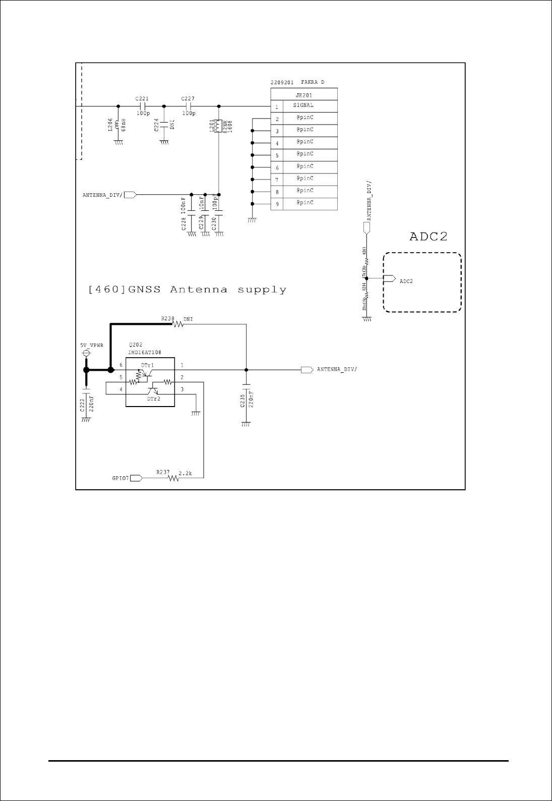
29/30
GPIO7 : GNSS POWER EN

30/30
<FCC Warning Statements>
FCC Part 15.19 Statements:
This device complies with Part 15 of the FCC Rules. Operation is subject to the following two
conditions: (1) this device may not cause harmful interference, and (2) this device must
accept any interference received, including interference that may cause undesired operation.
FCC Part 15.21 statement
Any changes or modifications not expressly approved by the party responsible for
compliance could void the user's authority to operate this equipment.
RF Exposure Statement
The antenna(s) must be installed such that a minimum separation distance of at least 20 cm
is maintained between the radiator (antenna) and all persons at all times. This device must
not be co-located or operating in conjunction with any other antenna or transmitter.
The highest permitted antenna gains including cable loss for use with this device are: GSM850 /
WCDMA850 : -3.25 dBi, GSM1900 / WCDMA1900 : 1.26 dBi, WCDMA1700 : -0.13 dBi, LTE Band 2:
1.26 dBi, LTE Band 5: -3.25 dBi, LTE Band 17: -3.03 dBi, LTE Band 4: -0.13 dBi, LTE Band 7: -0.22
dBi, LTE Band 12: -3.03 dBi..
End Product Labeling
The module is labeled with its own FCC ID. If the FCC ID is not visible when the module is
installed inside another device, then the outside of the device into which the module is
installed must also display a label referring to the enclosed module. In that case, the final
end product must be labeled in a visible area with the following:
“Contains FCC ID: BEJLGAJ10
OEM Responsibilities to comply with FCC Regulations
The module has been certified for integration into products only by OEM integrators under
the following condition:
- The antenna(s) must be installed such that a minimum separation distance of at least 20
cm is maintained between the radiator (antenna) and all persons at all times.
- The transmitter module must not be co-located or operating in conjunction with any other
antenna or transmitter except in accordance with FCC multi-transmitter product procedures.
As long as the two condition above is met, further transmitter testing will not be required.
However, the OEM integrator is still responsible for testing their end-product for any
additional compliance requirements required with this module installed (for example, digital
device emissions, PC peripheral requirements, etc.).
IMPORTANT NOTE: In the event that these conditions can ’t be met (for certain
configurations or co-location with another transmitter), then the FCC authorization is no
longer considered valid and the FCC ID can’t be used on the final product. In these
circumstances, the OEM integrator will be responsible for re-evaluating the end product
(including the transmitter) and obtaining a separate FCC authorization.
Manual Information To the End User
The OEM integrator has to be aware not to provide information to the end user regarding
how to install or remove this RF module or change RF related parameters in the user
manual of the end product.