LG Innotek TWFMB001T Wi-Fi Module User Manual Op Desc
LG Innotek Co., Ltd. Wi-Fi Module Users Manual Op Desc
UserManual.wiki
>
LG Innotek
>
TWFMB001T User Manual
>
Users Manual & Op Desc
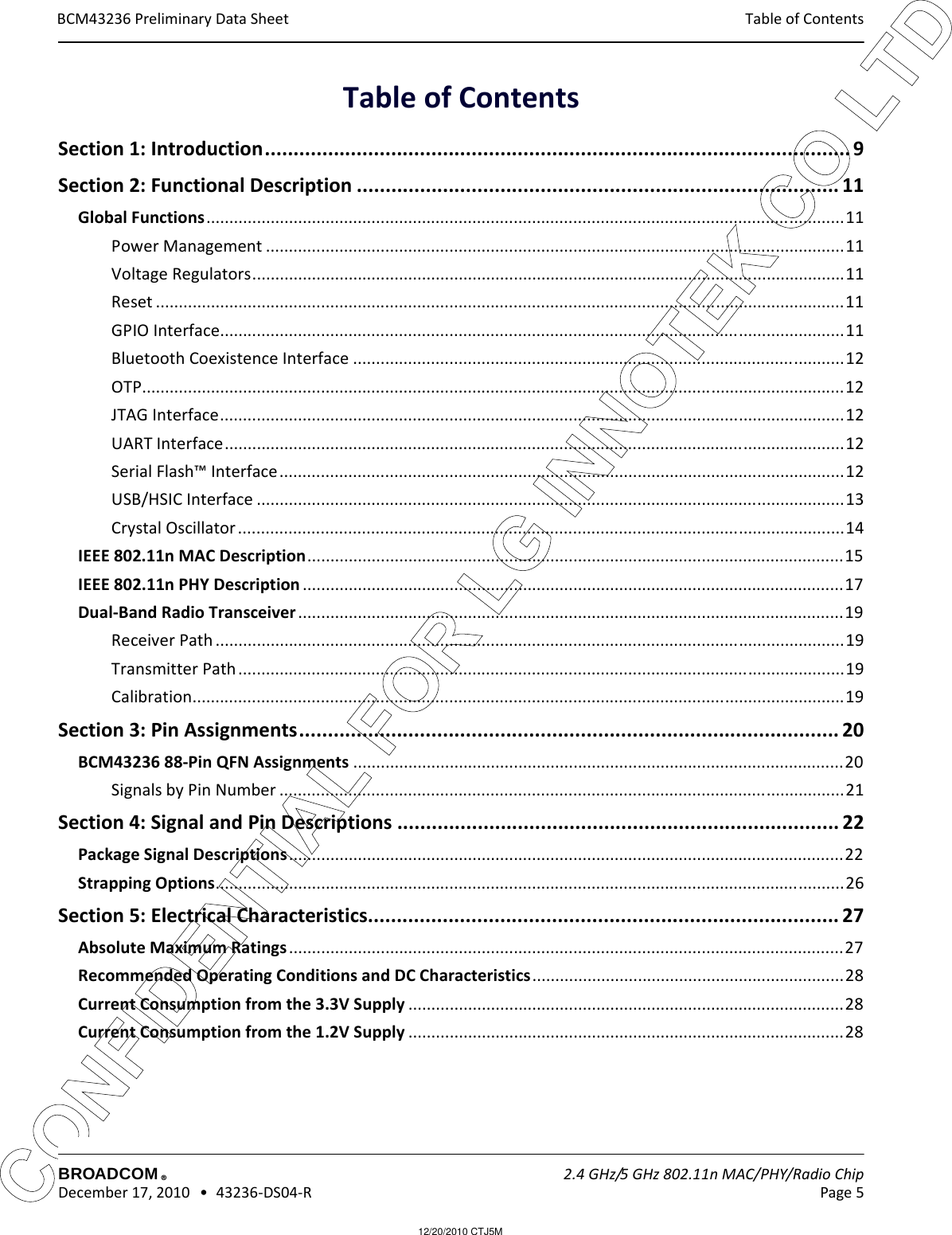
Contents
1.
Users Manual & Op Desc
2.
Operational Description and Manual
Users Manual & Op Desc
Navigation menu
Upload a User Manual
Namespaces
Wiki Guide
HTML
PDF
Info
Views
User Manual
Discussion / Help
Navigation
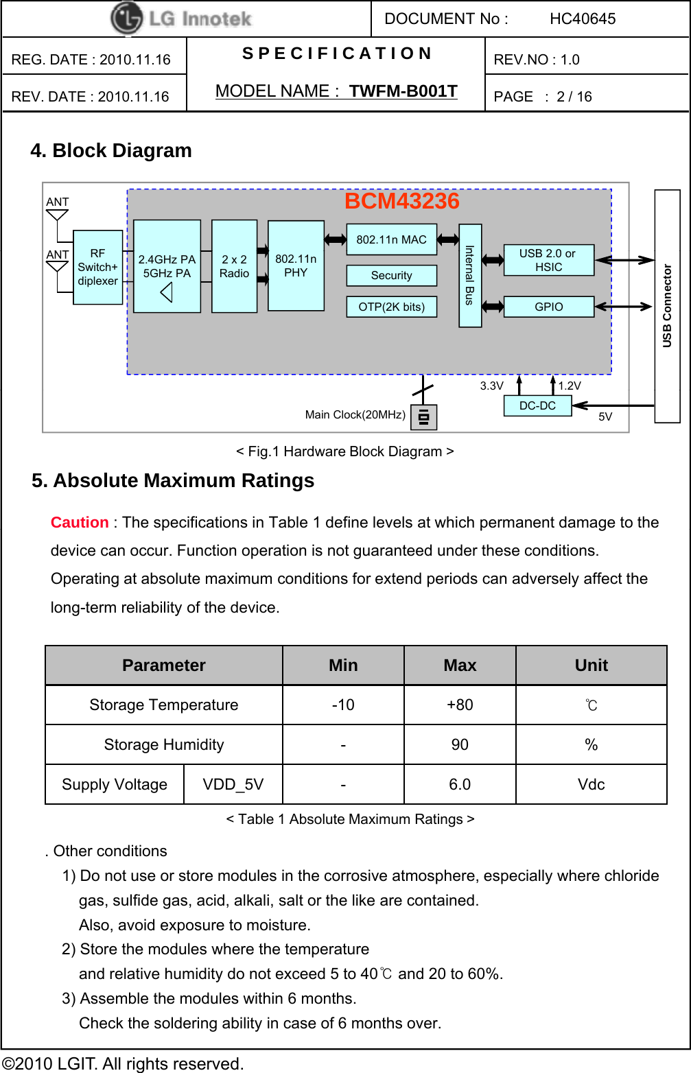
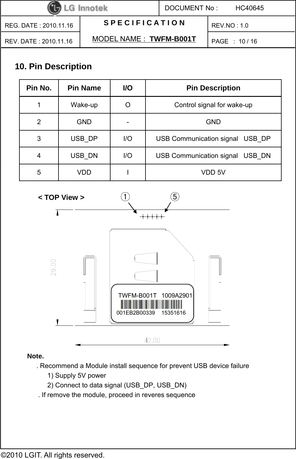
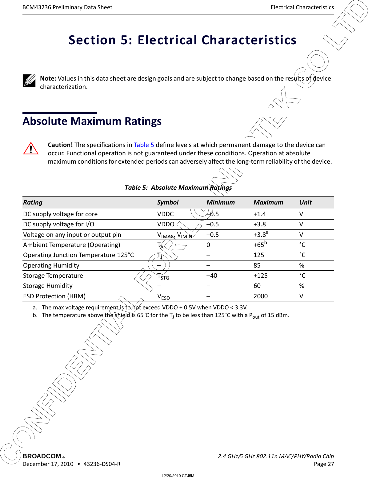
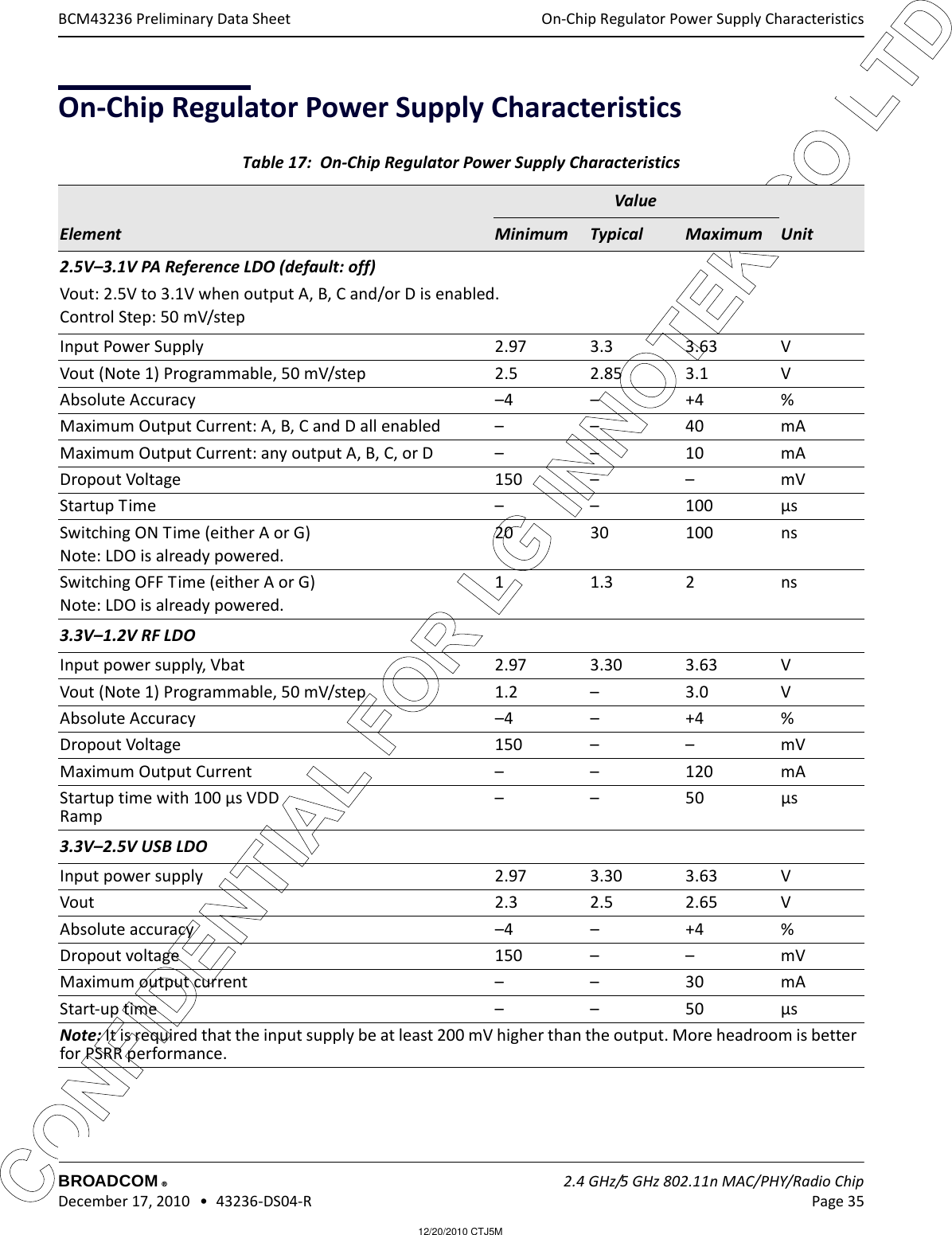
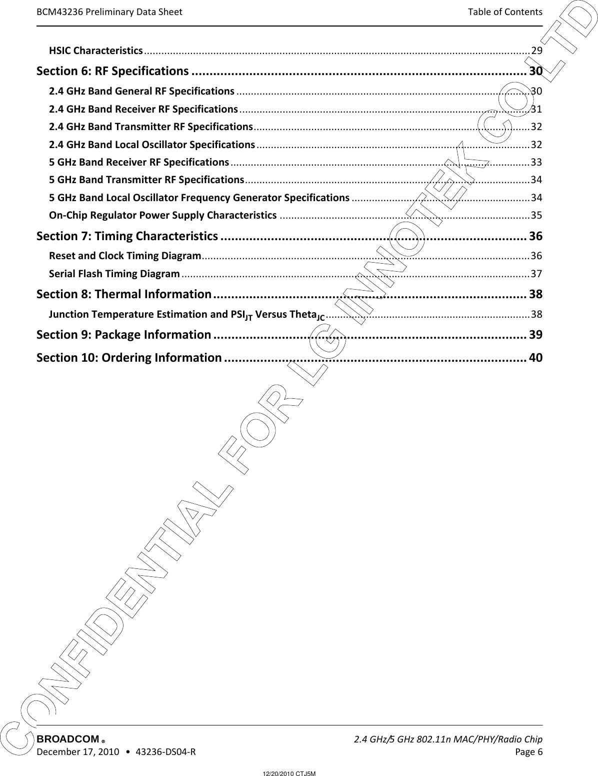
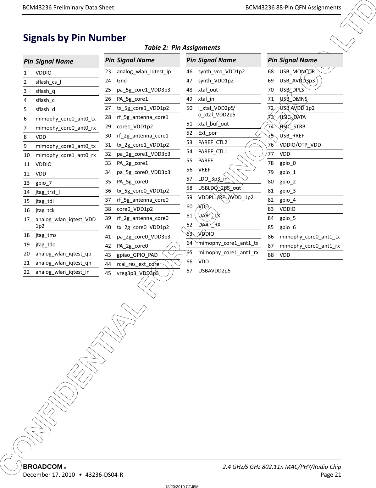
![S P E C I F I C A T I O NPAGE :DOCUMENT No :REG. DATE : 2010.11.16MODEL NAME : TWFM-B001TREV. DATE : 2010.11.16REV.NO : 1.0HC4064511 / 1611. S/WThe module is controlled by wl command. It is intended for those evaluating and/or testing Broadcom’s IC, describes a subset of the commands available in wl, the Broadcom ® WLAN client utility.1) Command SyntaxThe syntax is as follows:wl <adapter> [-h] [-d|u|x] <command> [arguments]where-h this message and command descriptions-d output format signed integer-u output format unsigned integer-x output format hexdecimalThe [h,u] option is only to print help.Other syntax specifics are as follows:• Entries within square brackets, such as [arguments], are optional. In the above example,switches within brackets, such as –h, are typed as shown. The |symbol should not be typed, it represents the word or.• Entries within angle brackets, such as <adapter>, are required and indicate that a value must be inserted in place of the item contained within the angle brackets.•Entries shown outside of either square or angle brackets are to be typed as shownEntries shown outside of either square or angle brackets are to be typed as shown.2) Command List and Version•CMDSSyntax: wl cmdsPurpose: Generates a list of available commands.pParameters:NoneReturns: All commands available to the attached 43XX chip.•VERSyntax: wl verPurpose: Generates a list of available commands.Parameters:None©2010 LGIT. All rights reserved.Parameters:NoneReturns: All commands available to the attached 43XX chip.•Please refer to ‘80211-TI201-R’ technical document of Broadcom to other commands.](https://usermanual.wiki/LG-Innotek/TWFMB001T.Users-Manual-Op-Desc/User-Guide-1395061-Page-12.png)
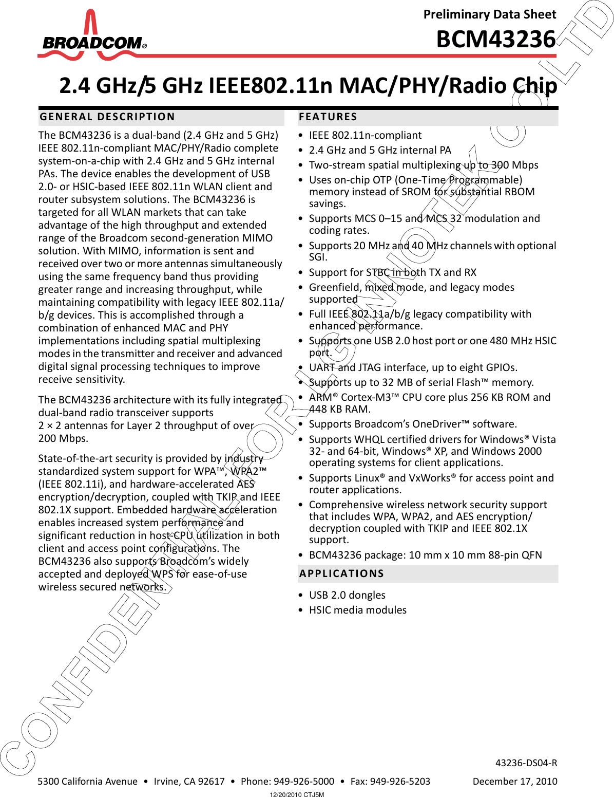
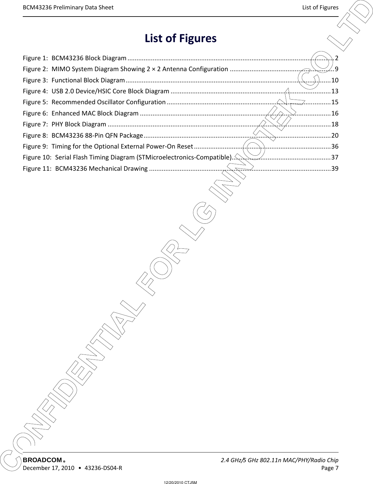
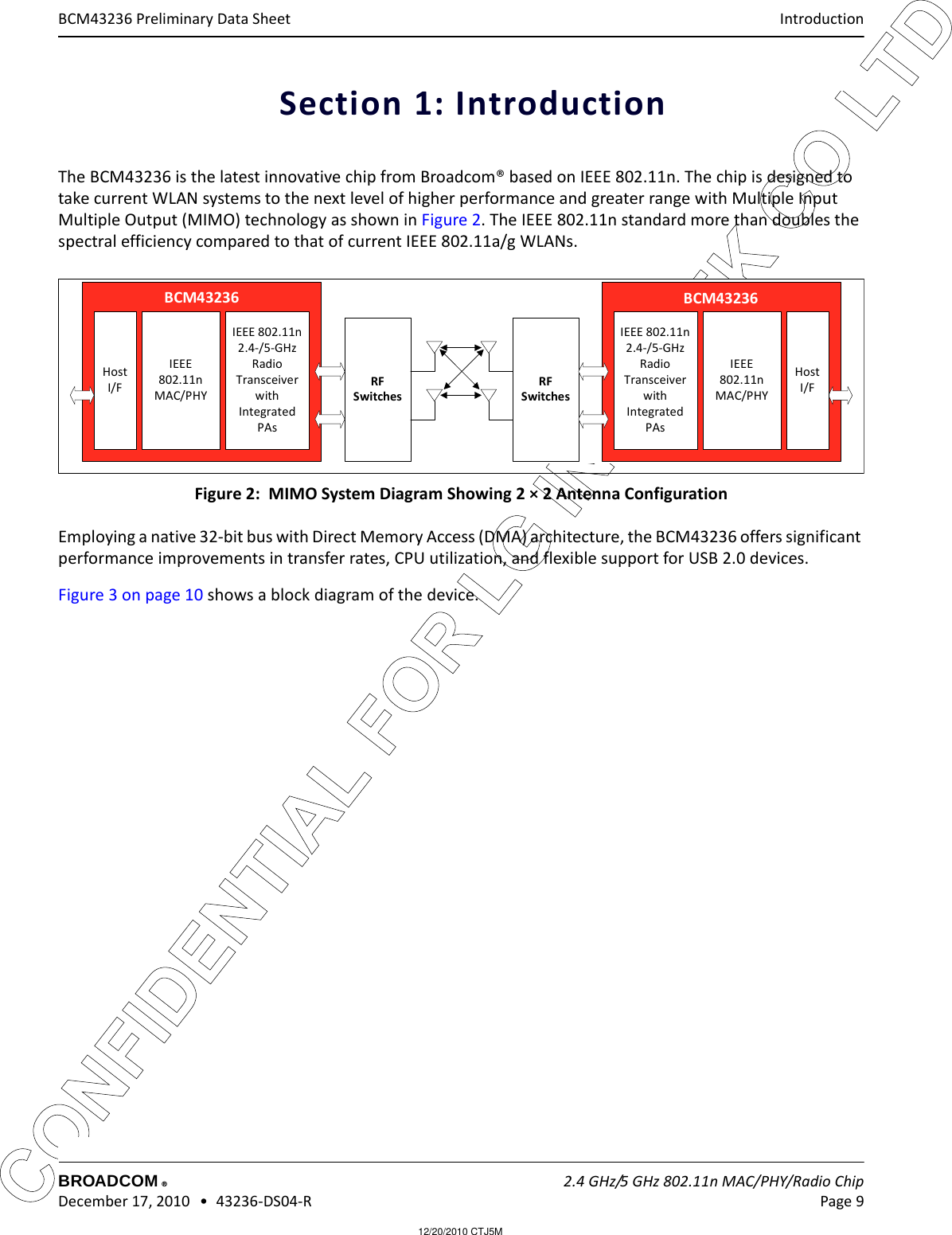
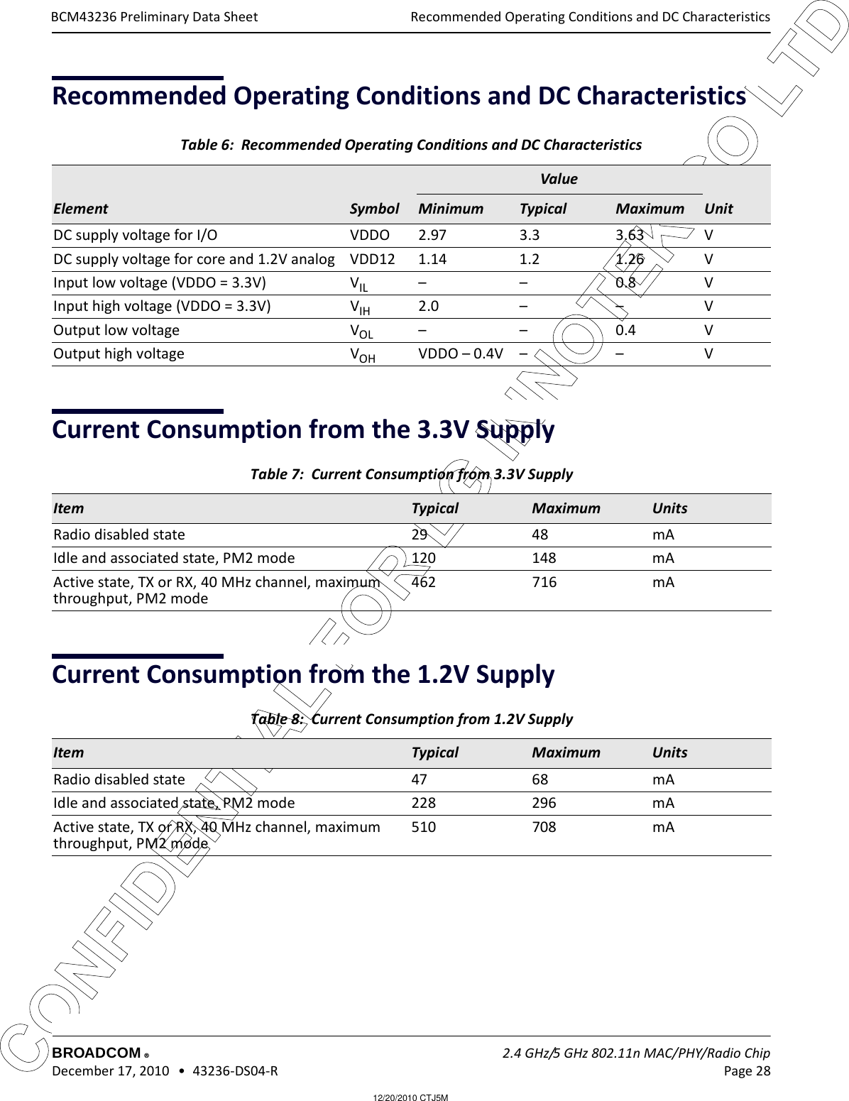
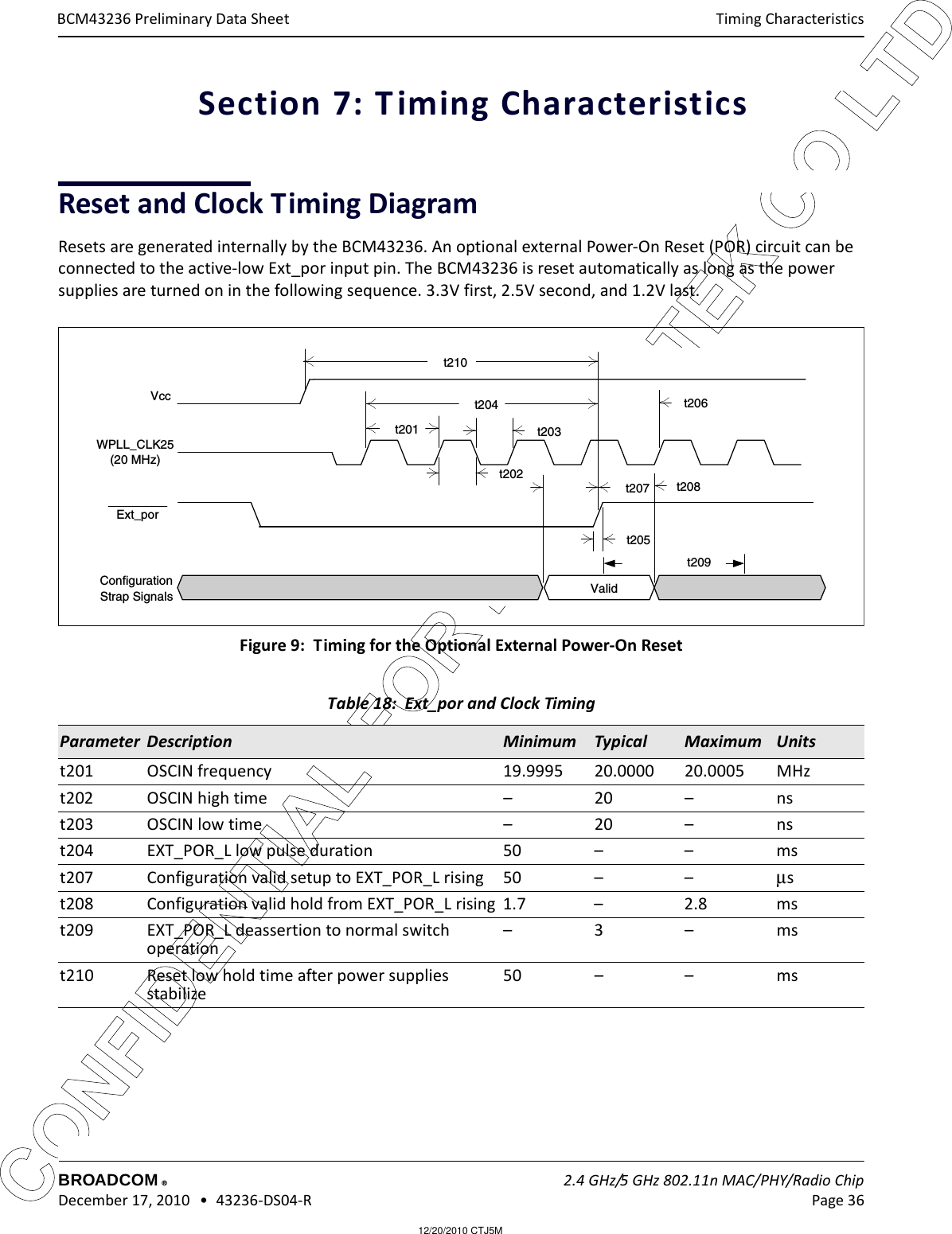
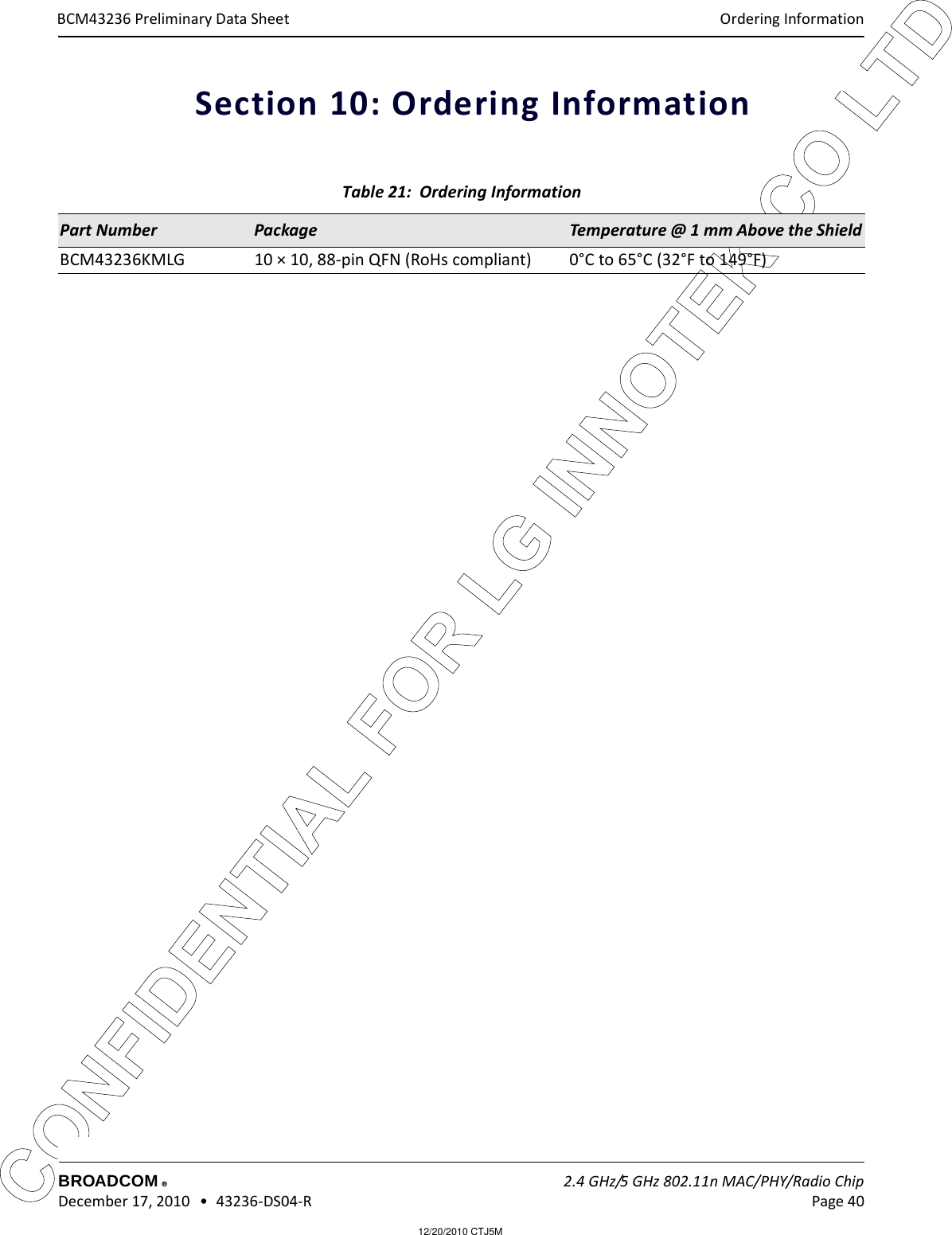
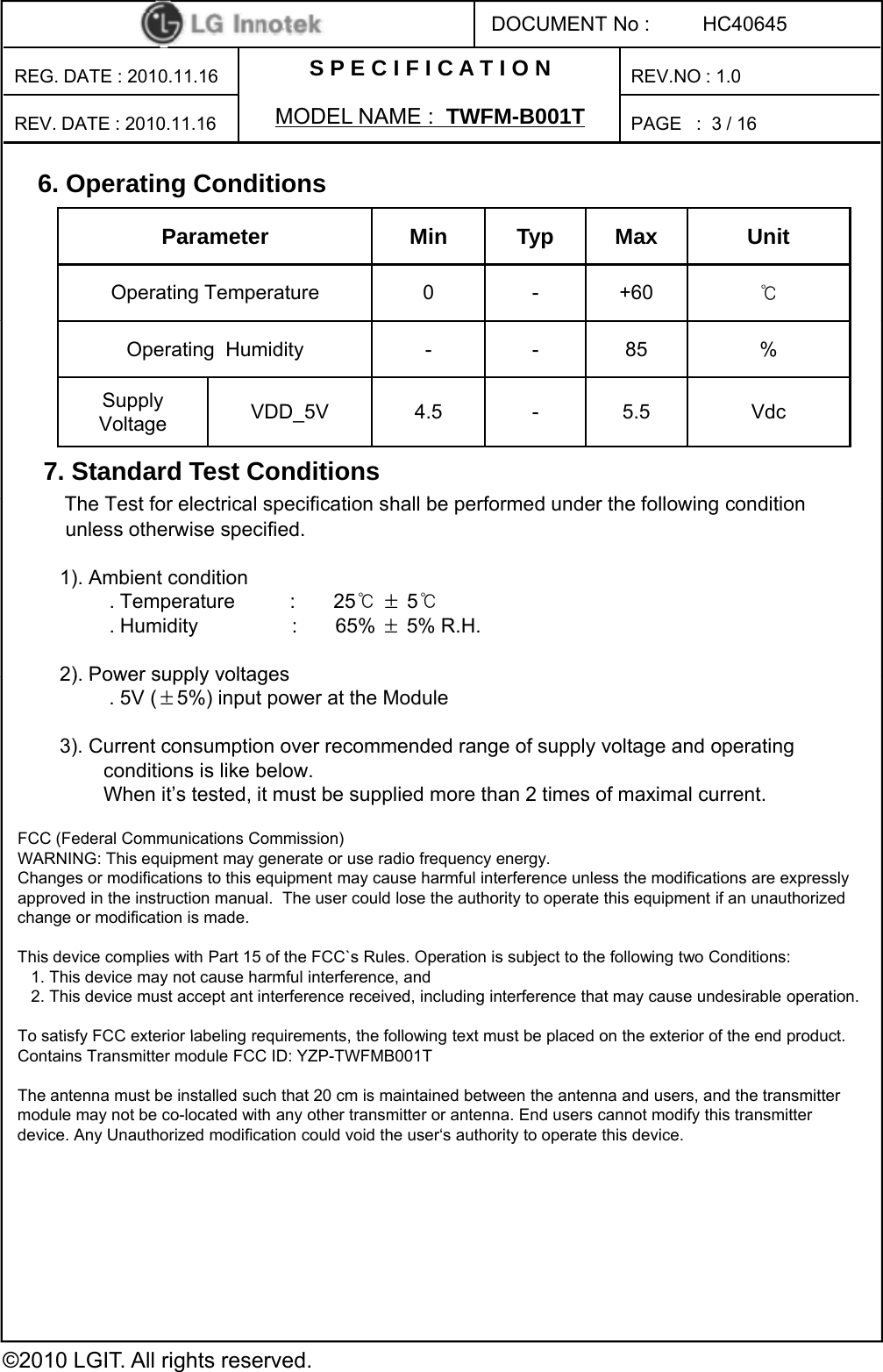
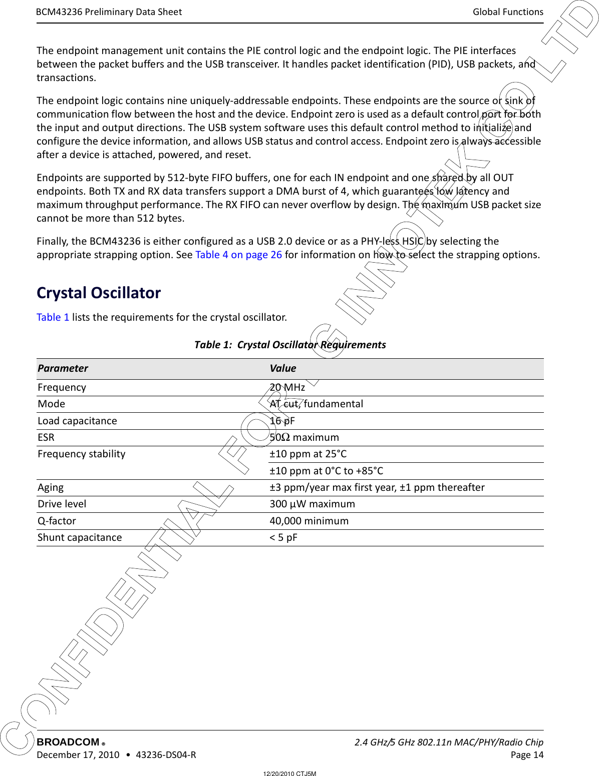
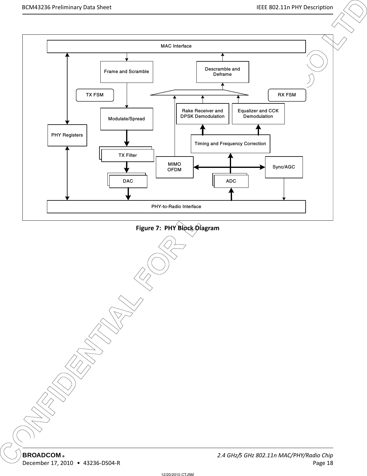
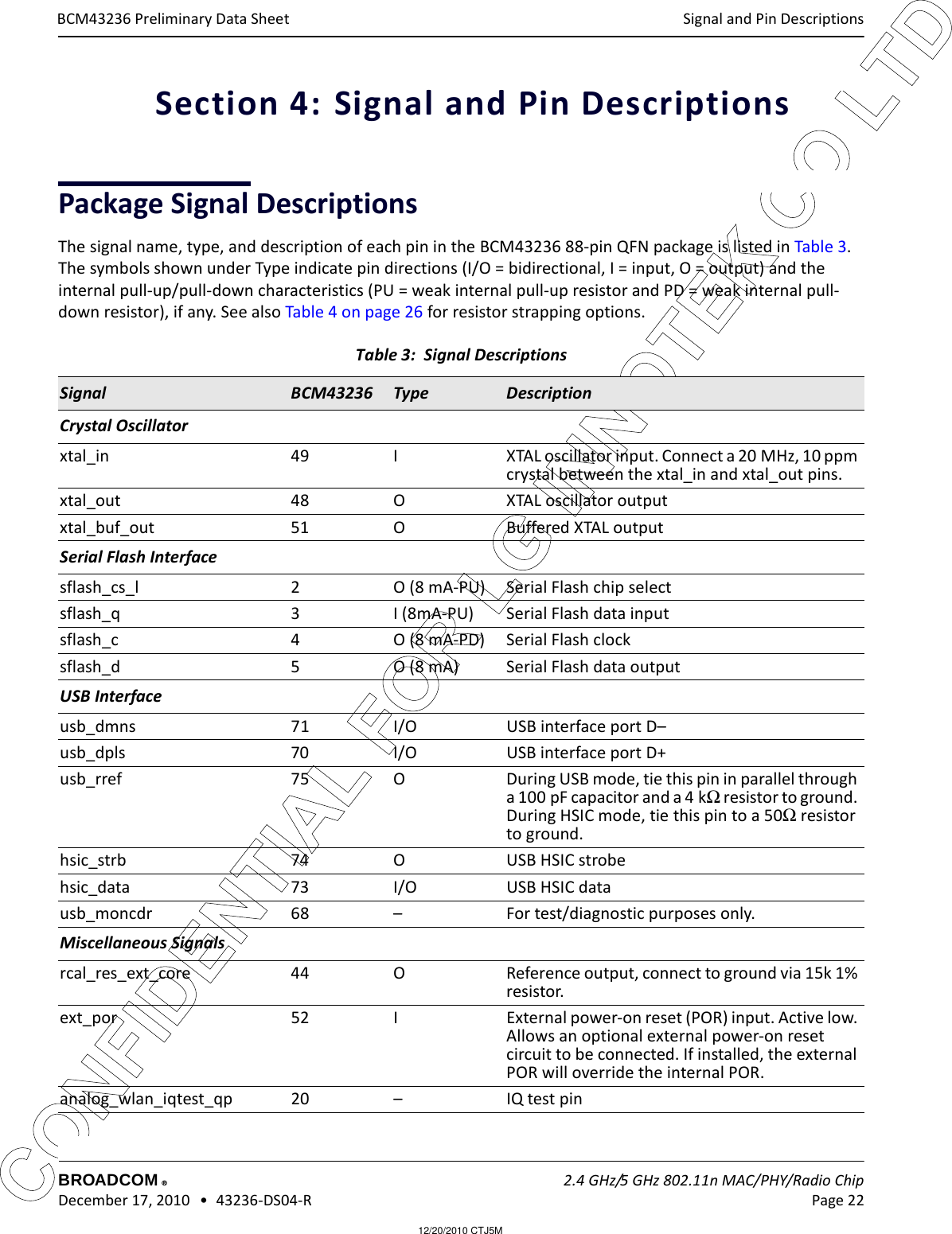
![12/20/2010 CTJ5MCONFIDENTIAL FOR LG INNOTEK CO LTD IntroductionBROADCOM 2.4 GHz/5 GHz 802.11n MAC/PHY/Radio Chip December 17, 2010 • 43236-DS04-R Page 10®BCM43236 Preliminary Data SheetFigure 3: Functional Block DiagramBCM43236Internal Bus SystemIEEE802.11nPHY2.4/5 GHz RadioSecurityRFControlUARTJTAGInterfaceUART_RXUART_TXGPIOPLL 20 MHz Ref. ClockSFLASH InterfaceROM(256 KB)ARMCortexM3RAM(448 KB)USB 2.0Deviceor HSICIEEE 802.11nMACGPIO[0:7]antenna switch controls (10)ext_lna_2g controls (4)ext_lna_5g controls (4)pa_2g controls (2)pa_5g controls (2)USB20_DEV_DPLSUSB20_DEV_DMNSHSIC DataHSIC StrobeTRST#TMSTDITCLKTDOtssiln_0tssiln_1lna_p_a_0lna_p_a_1lna_p_g_0lna_p_g_0pa_p_a_0pa_p_a_1pa_p_g_0pa_p_g_1xtal_buf_outxtal_outxtal_insflash_dextif_flash_cs_lsflash_csflash_q](https://usermanual.wiki/LG-Innotek/TWFMB001T.Users-Manual-Op-Desc/User-Guide-1395061-Page-22.png)
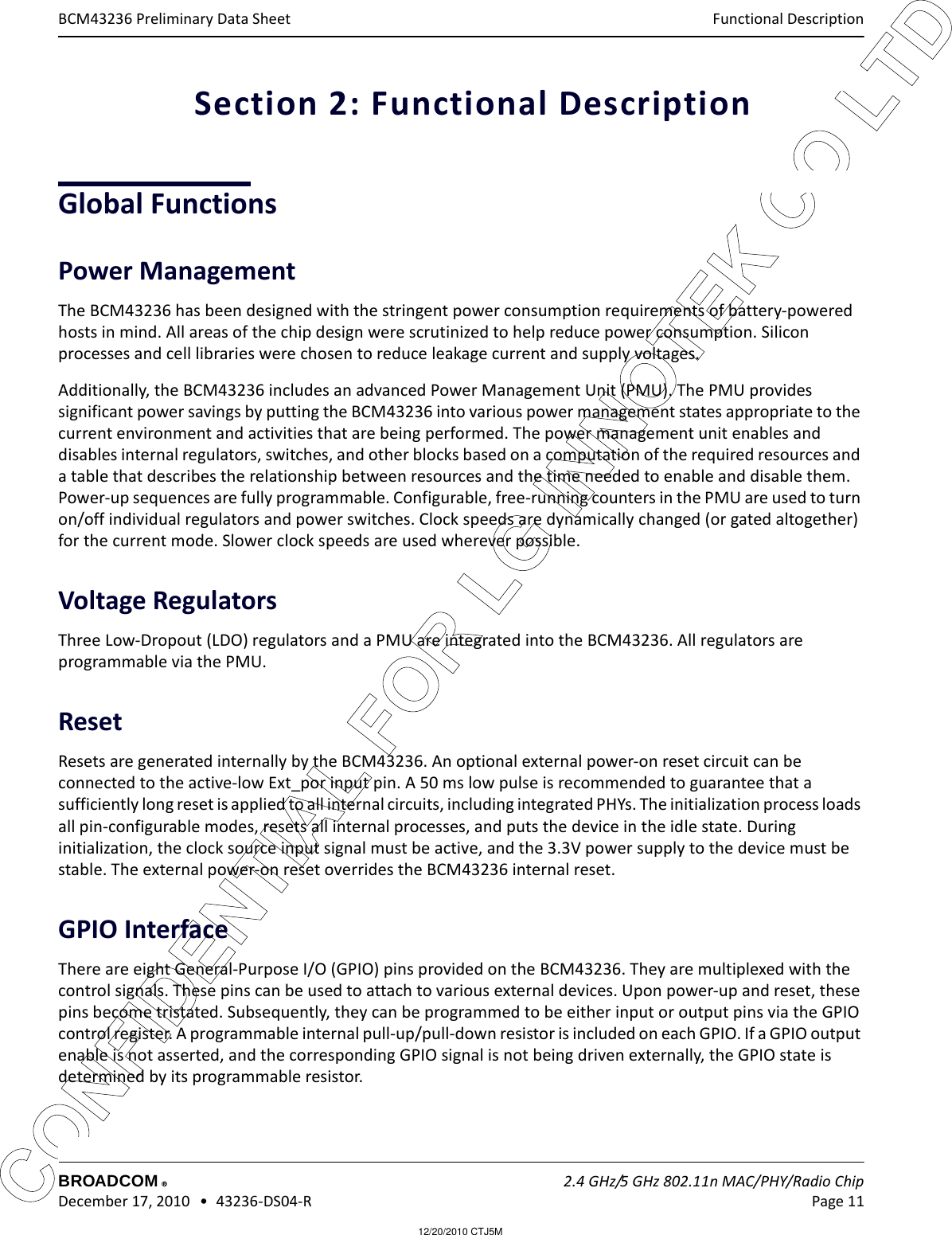
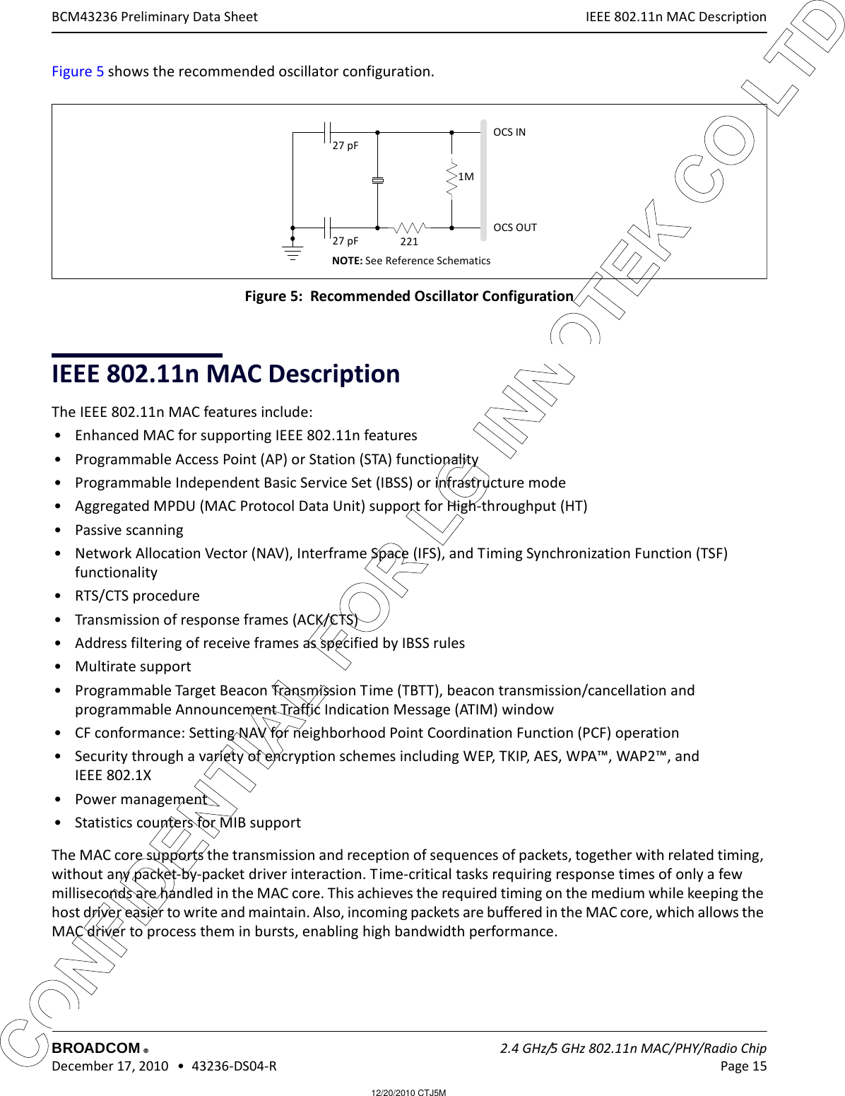
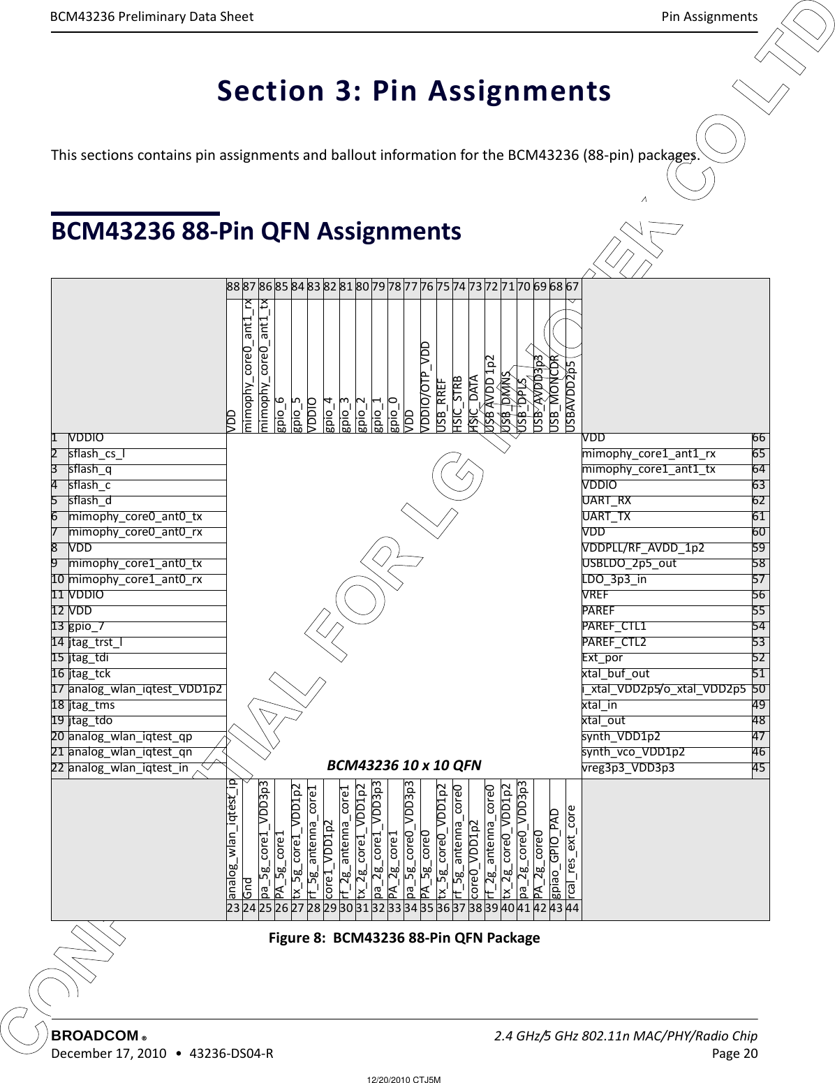
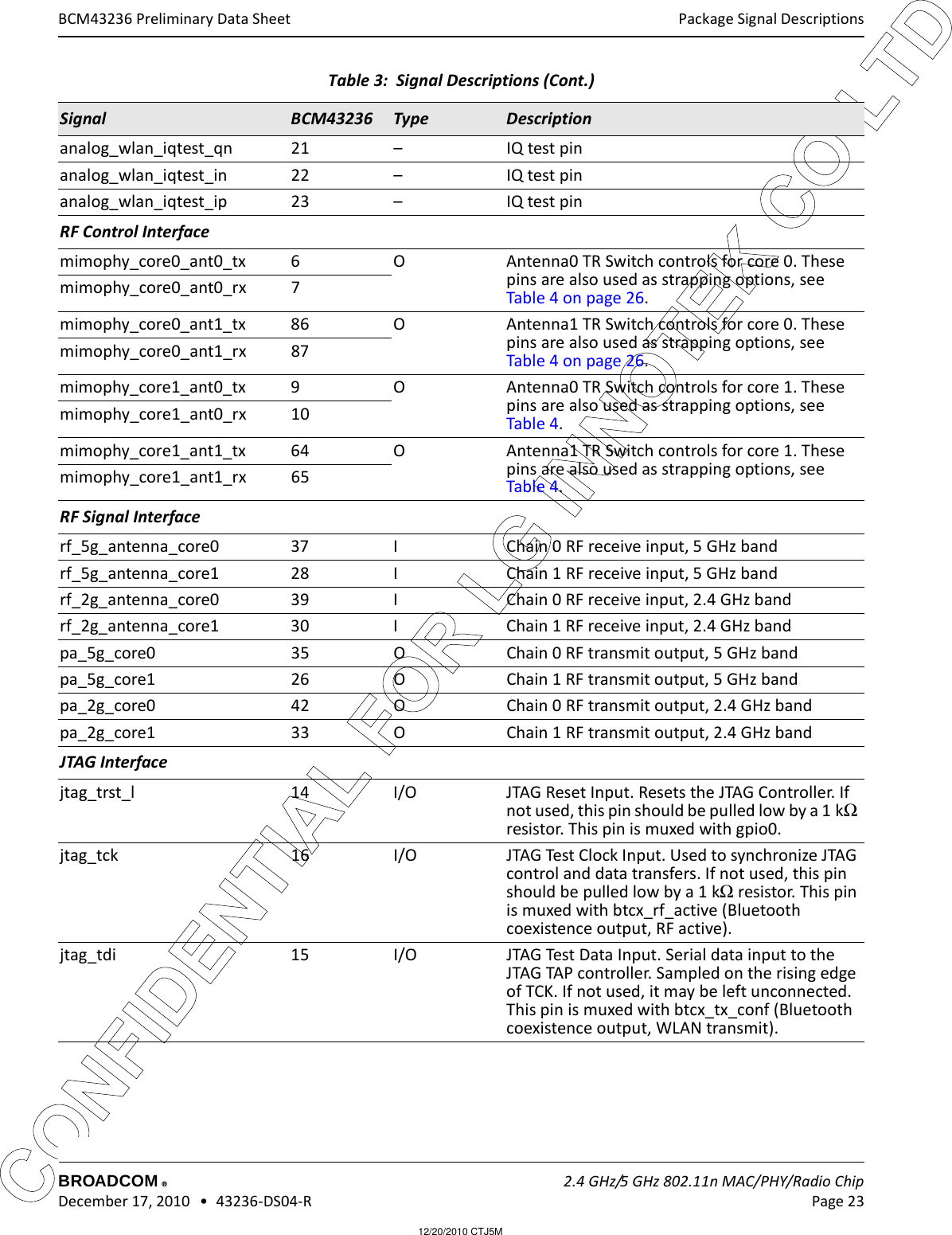
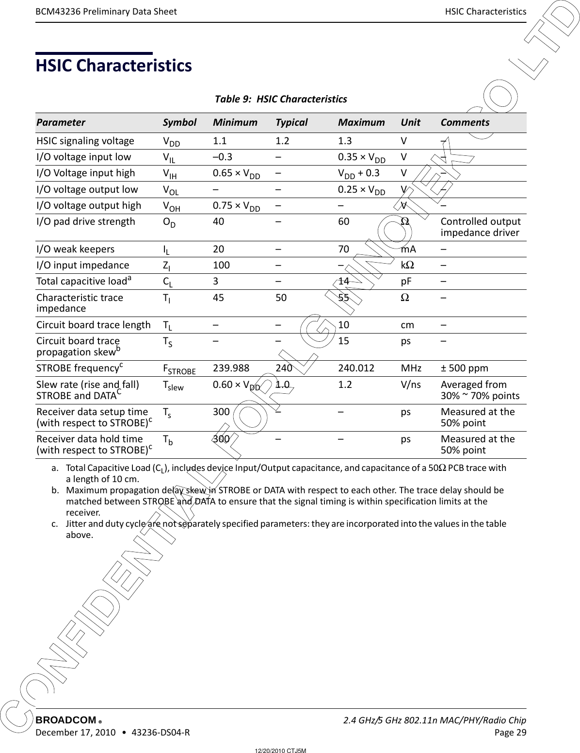
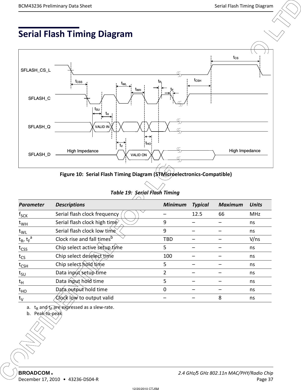
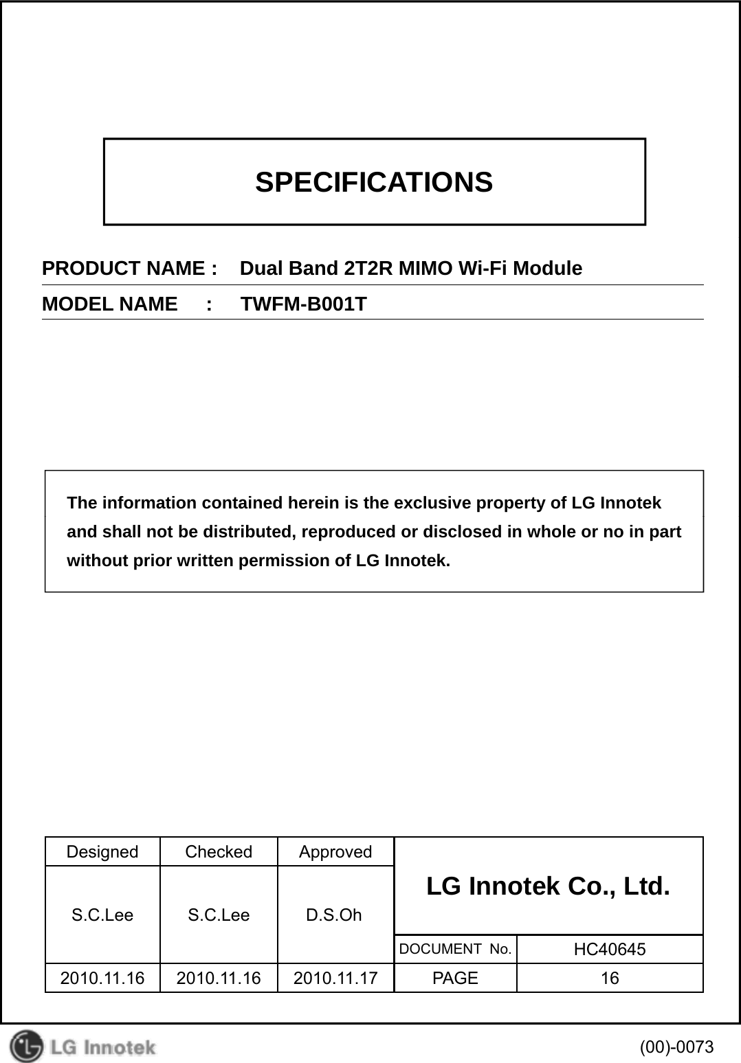
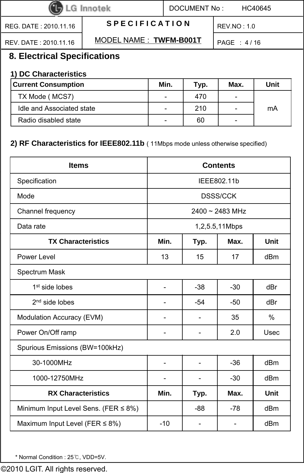
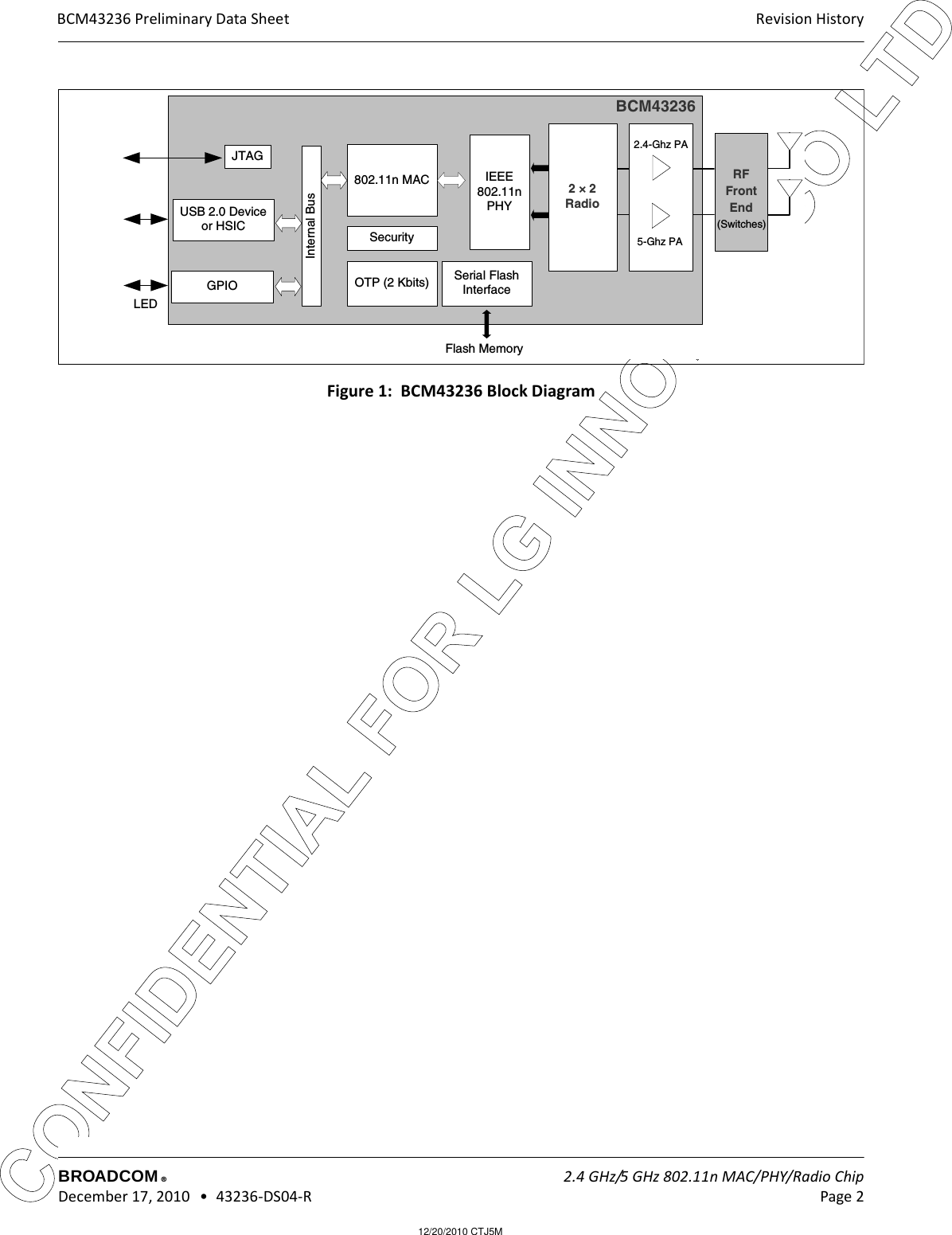
![12/20/2010 CTJ5MCONFIDENTIAL FOR LG INNOTEK CO LTD Package Signal DescriptionsBROADCOM 2.4 GHz/5 GHz 802.11n MAC/PHY/Radio Chip December 17, 2010 • 43236-DS04-R Page 24®BCM43236 Preliminary Data Sheetjtag_tdo 19 I/O JTAG Test Data Output. Serial data output from the JTAG TAP controller. Sampled on the rising edge of TCK. If not used, it may be left unconnected. This pin is muxed with btcx_prisel (Bluetooth coexistence output, antenna select).jtag_tms 18 I/O JTAG Mode Select Input. Single control input to the JTAG TAP controller used to traverse the test logic state machine. Sampled on the rising edge of TCK. If not used, it may be left unconnected. This pin is muxed with btcx_status (Bluetooth coexistence output, status).GPIO Interfacegpio_0 78 I/O (8 mA)General Purpose I/O pin. This pin is tristated on power-up and reset. Subsequently, it becomes an input or an output through software control. A programmable PU or PD resistor is available for each GPIO pin. This pin is muxed with wlan_led (WLAN LED output).gpio_1 79 I/O General Purpose I/O pin. This pin is muxed with mimophy_core0_ant_shd (antenna switch control for the shared [middle] antenna of a 2 of 3 design [core 0]).gpio_2 80 I/O General Purpose I/O pin. This pin is muxed with: • mimophy_core1_ant_shd: antenna switch control for the shared (middle) antenna of a 2 of 3 design (core 1).• btcx_freq: Bluetooth coexistence RF frequencygpio_3 81 I/O General Purpose I/O pin.gpio_4 82 I/O General Purpose I/O pin. This pin is muxed with:• ext_lna_2g_pu_0: 2.4 GHz band core 0 power amplifier control• ext_pa_2g_0: 2.4 GHz band core 0 power amplifier control• CS: SPI selectgpio_5 84 I/O General Purpose I/O pin. This pin is muxed with:• ext_lna_2g_pu_1: 2.4 GHz band core 1 power amplifier control• ext_pa_2g_1: 2.4 GHz band core 1 power amplifier control•SCLK: SPI clock•I2C_SCL: I2C clockTable 3: Signal Descriptions (Cont.)Signal BCM43236 Type Description](https://usermanual.wiki/LG-Innotek/TWFMB001T.Users-Manual-Op-Desc/User-Guide-1395061-Page-36.png)
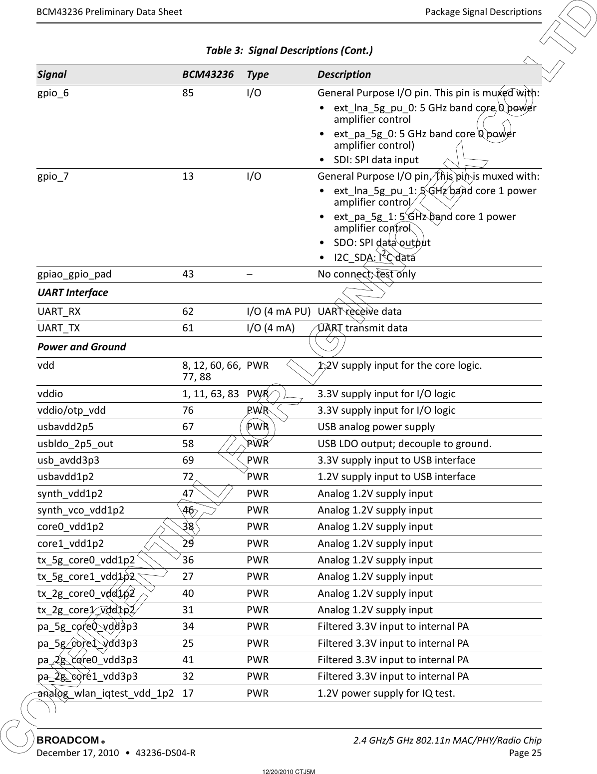
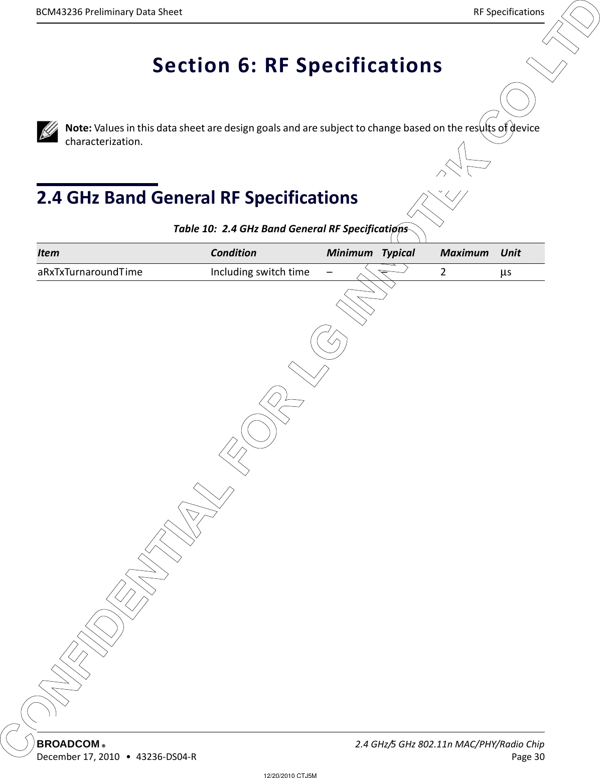
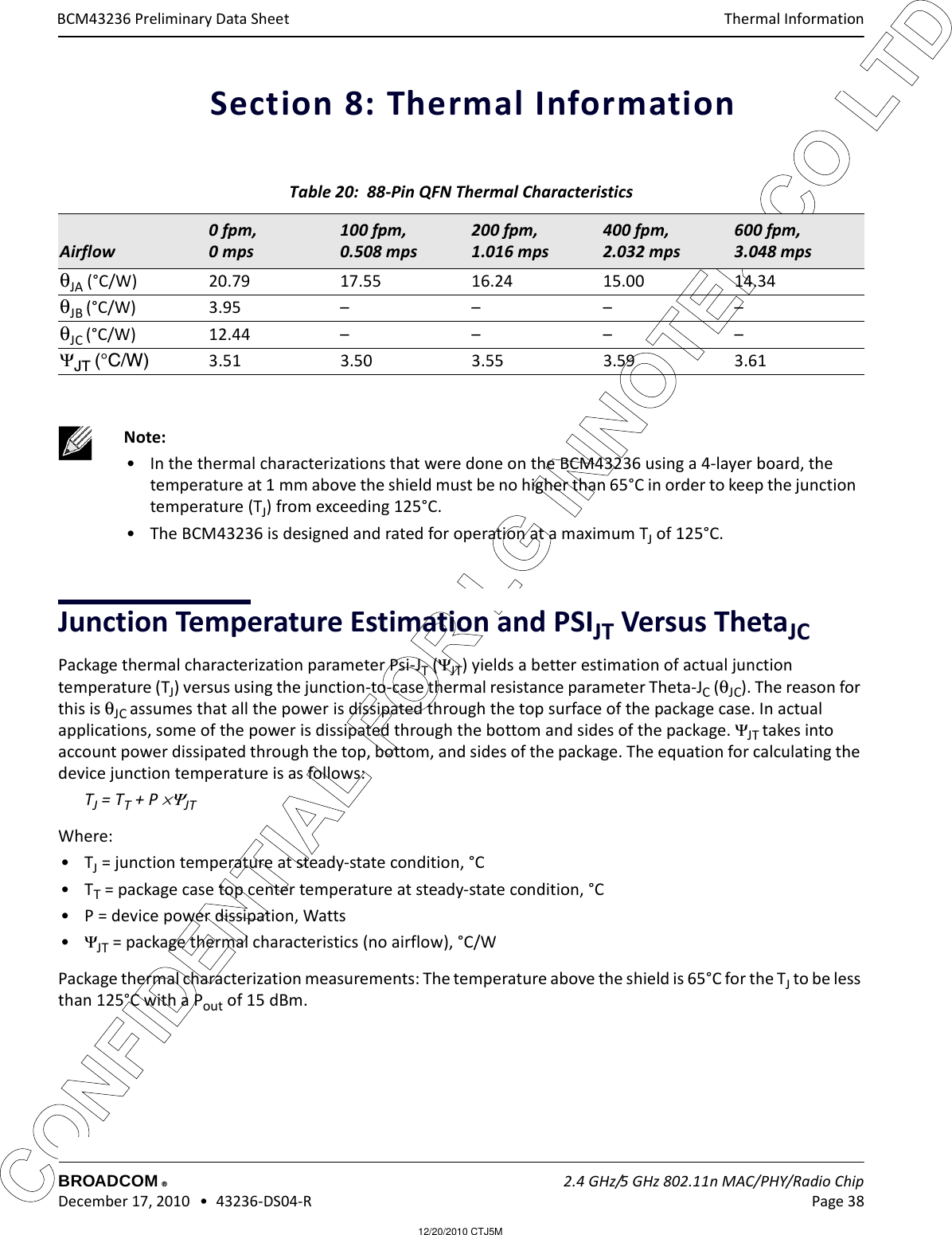
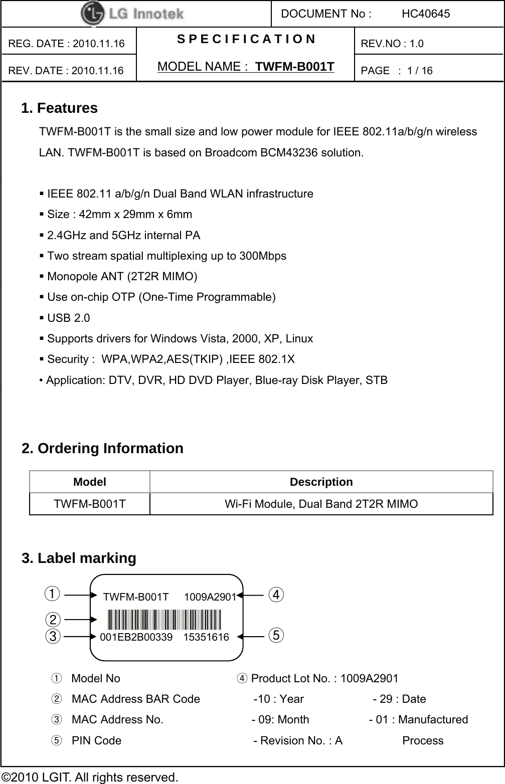
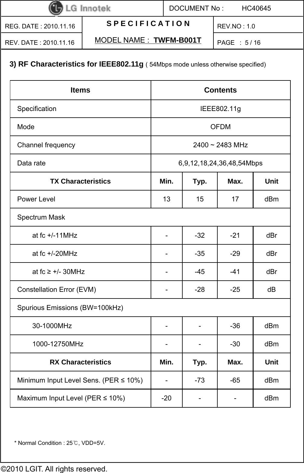
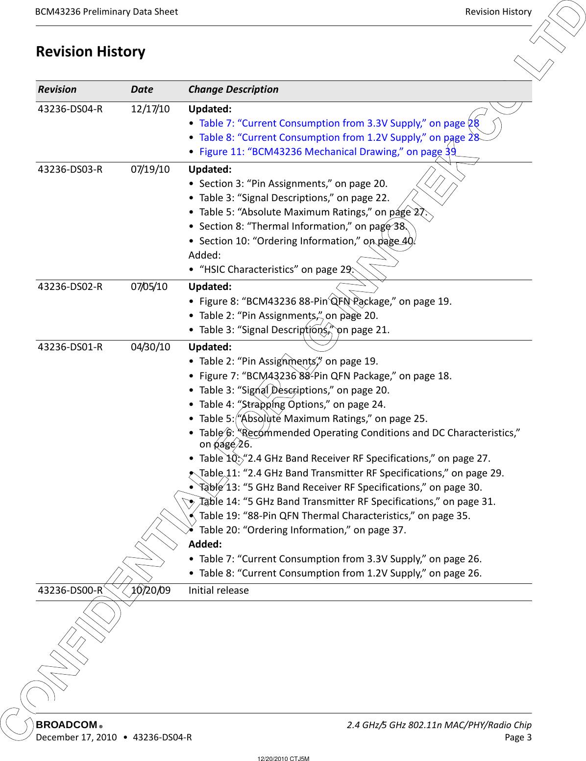
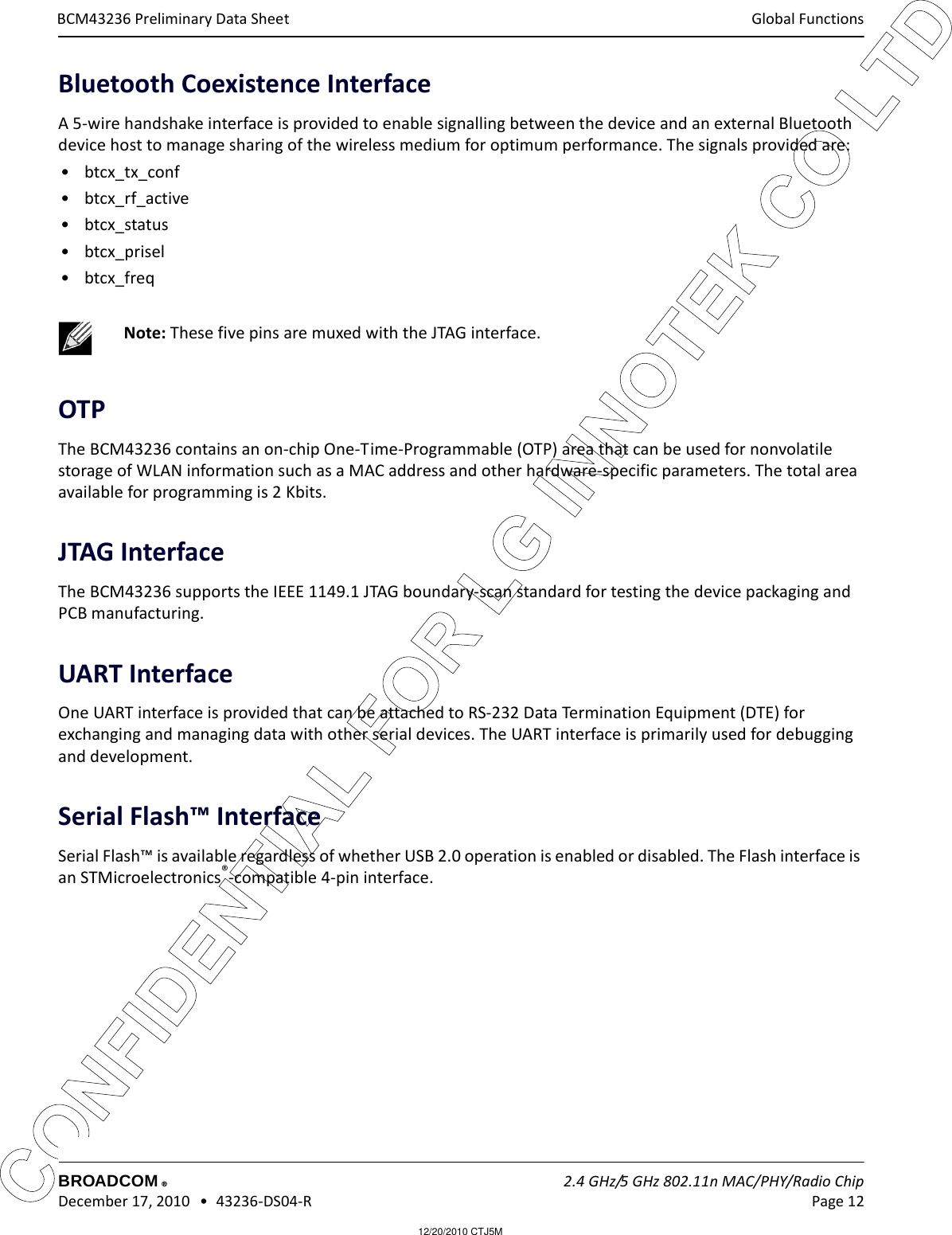
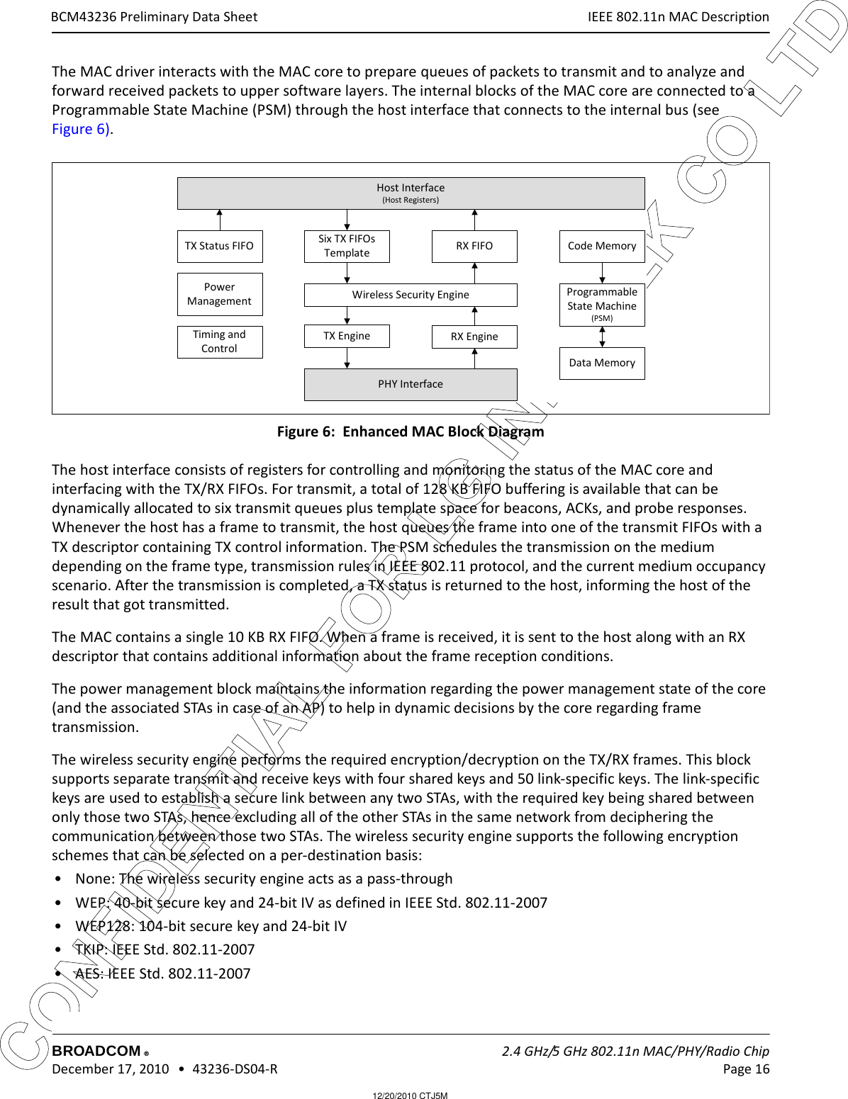
![12/20/2010 CTJ5MCONFIDENTIAL FOR LG INNOTEK CO LTD Strapping OptionsBROADCOM 2.4 GHz/5 GHz 802.11n MAC/PHY/Radio Chip December 17, 2010 • 43236-DS04-R Page 26®BCM43236 Preliminary Data SheetStrapping OptionsThe pins listed in Table 4 are sampled at Power-on Reset (POR) to determine the various operating modes. Sampling occurs within a few milliseconds following internal POR or deassertion of external POR. After POR, each pin assumes the function specified in the signal descriptions table. Each pin has an internal pull-up (PU) or pull-down (PD) resistor that determines the default mode. To change the mode, connect an external PU resistor to VDDIO or a PD resistor to GND; use 10 kΩ or less (refer to the reference board schematics for further details).ldo_3p3_in 57 PWR 3.3V input to RF LDOvddpll/rf_avdd_1p2 59 O XTAL power reference; decouple to ground.vreg3p3_vdd3p3 45 PWR Analog 3.3V supplyi_xtal_vdd2p5/o_xtal_vdd2p5 50 PWR 3.3V supply input for I/O logicvref 56 – VREF; decouple to ground.paref 55 – PA reference; decouple to ground.paref_ctl1 54 – PA reference control 1paref_ctl2 53 – PA reference control 2gnd_slug H GND Groundgnd 24 GND GroundTable 4: Strapping Options Signal Name Mode Default Description mimophy_core0_ant0_tx OTP select PU 0: No OTP1: OTP presentmimophy_core1_ant0_tx SFLASH not presentPD 0: SFLASH not present1: SFLASH presentmimophy_core0_ant0_rx ST SFLASH PD 0: SFLASH type is STMicroelectronics1: SFLASH type is Atmel®mimophy_core0_ant1_tx USB PHY PU 0: HSIC mode1: USB PHY modemimophy_core0_ant1_rx 120 MHz PU 0: Backplane at 96 (98.4) MHz1: Backplane at 120 (123) MHzgpio[7:6] Boot from ROM No pull 00: Remap to RAM; ARM processor to be held at reset.01: Boot from ROM unless the ARM needs to be held at reset.Table 3: Signal Descriptions (Cont.)Signal BCM43236 Type Description](https://usermanual.wiki/LG-Innotek/TWFMB001T.Users-Manual-Op-Desc/User-Guide-1395061-Page-38.png)