LITE ON TECHNOLOGY BSM700 Bluetooth Module User Manual BSM 700 BT4 0 Spec ver1 3
LITE-ON Technology Corp. Bluetooth Module BSM 700 BT4 0 Spec ver1 3
UserManual.wiki
>
LITE ON TECHNOLOGY
>
BSM700 User Manual
User manual
Navigation menu
Upload a User Manual
Namespaces
Wiki Guide
HTML
PDF
Info
Views
User Manual
Discussion / Help
Navigation
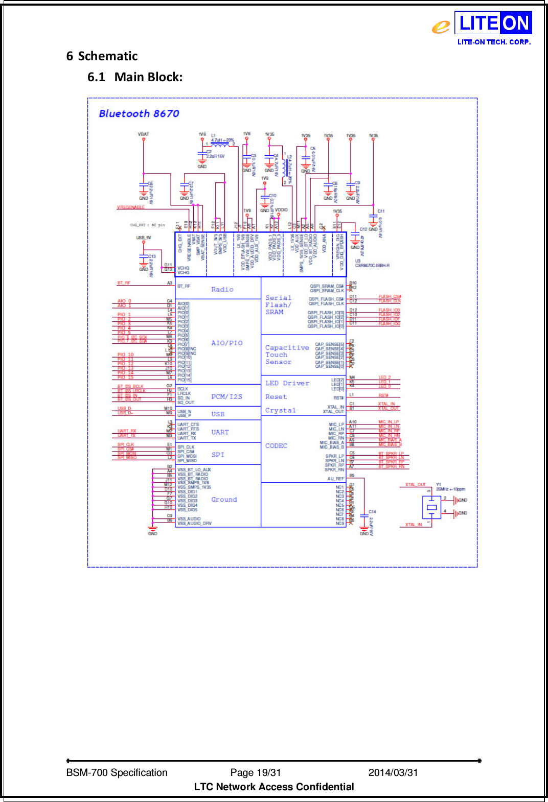
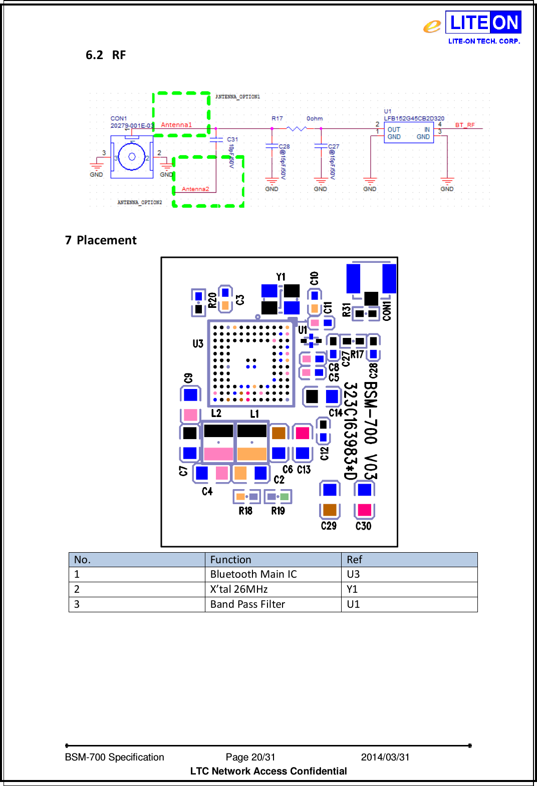
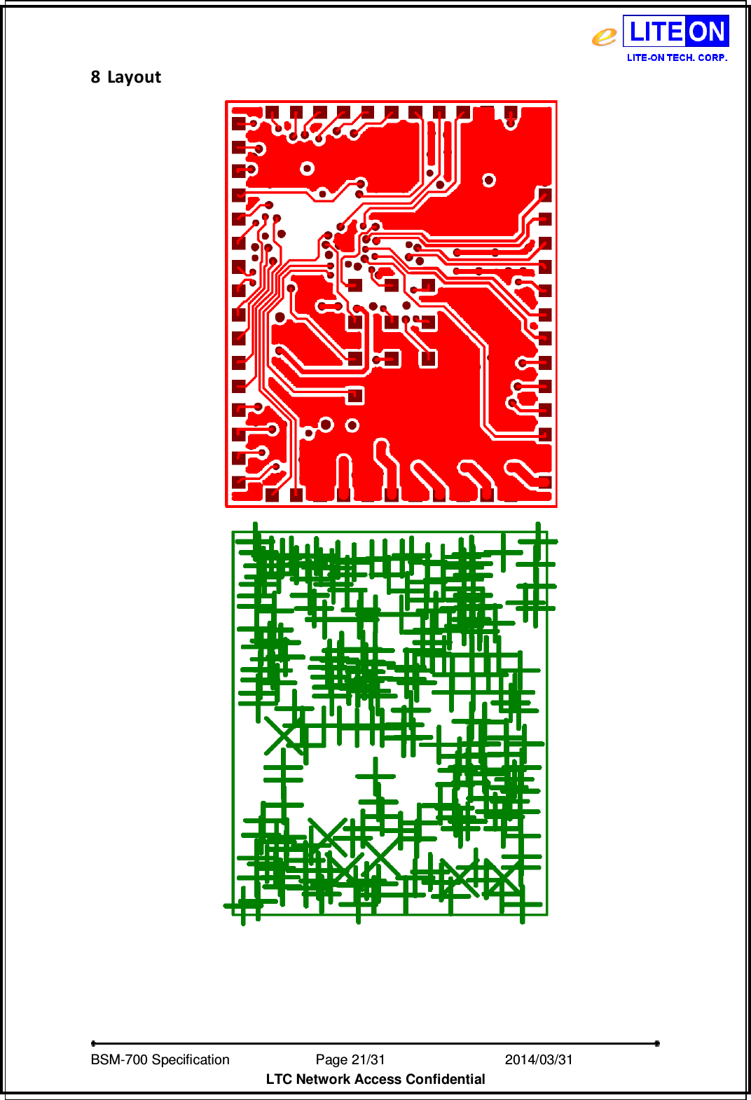
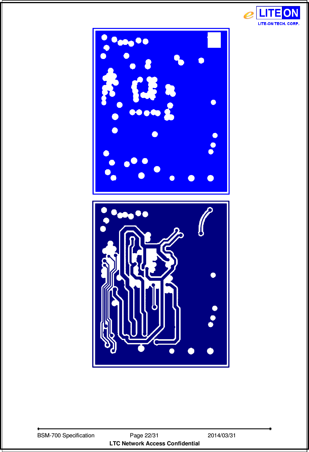
![BSM-700 Specification Page 1/31 2014/03/31 LTC Network Access Confidential PRODUCT SPECIFICATION CSR8670 Full function Bluetooth Module BSM-700 Lite-On P/N: 2170000002KD Version 1.3 Author: Action Cheng Editor: Javon Tseng Project Leader: Daniel KW Yang Approved by: Daniel KW Yang Change History Revision Date Author Change List Version 1.0 2014 / 01 / 13 Javon Tseng Preliminary Version1.1 2014 /01 / 24 Daniel 1. Add pinout dimensions 2. Remove NC (Pin57) and connect AIO[0] to PIN 57. 3. Remove PIO0 (Pin4) and connect AIO[1] to PIN 4 4. Add PIO_3 to PIN60 Version1.2 2014 /02 / 06 Javon 1. Update Block Diagram 2. Update Application block diagram 3. Update main board schematic Version1.3 2014 /04 / 03 Javon 1. Add Packing Model 2. Update Current Consumption 3. Update Package Dimensions 4. Update RF Characteristics 5. Update Interface Specifications 6. Update Layout * This document contains confidential proprietary information and is property of LTC. The contents of this document should not be disclosed to unauthorized persons without the written consent of LTC.](https://usermanual.wiki/LITE-ON-TECHNOLOGY/BSM700/User-Guide-2266335-Page-1.png)
![BSM-700 Specification Page 5/31 2014/03/31 LTC Network Access Confidential 1.4 Block Diagram 1.5 Pin Configuration No Definition Description Type 1 UART_RX UART data in Bidirectional with strong pull-up 2 UART_TX UART data output Bidirectional with weak pull-up 3 LED_0 LED driver[0] Open drain 4 AUO[1] Programmable input / output line Analogue programmable input / output line 5 LED_2 LED driver[2] Open drain 6 PIO_6_I2C_SCK Programmable input / output line Bidirectional with weak pull-down 7 USB_D+ USB data plus with selectable internal 1.5kΩ pull-up resistor Bidirectional 8 USB_D- USB data minus Bidirectional 9 PIO_2 Programmable input / output line Bidirectional with weak pull-down](https://usermanual.wiki/LITE-ON-TECHNOLOGY/BSM700/User-Guide-2266335-Page-5.png)
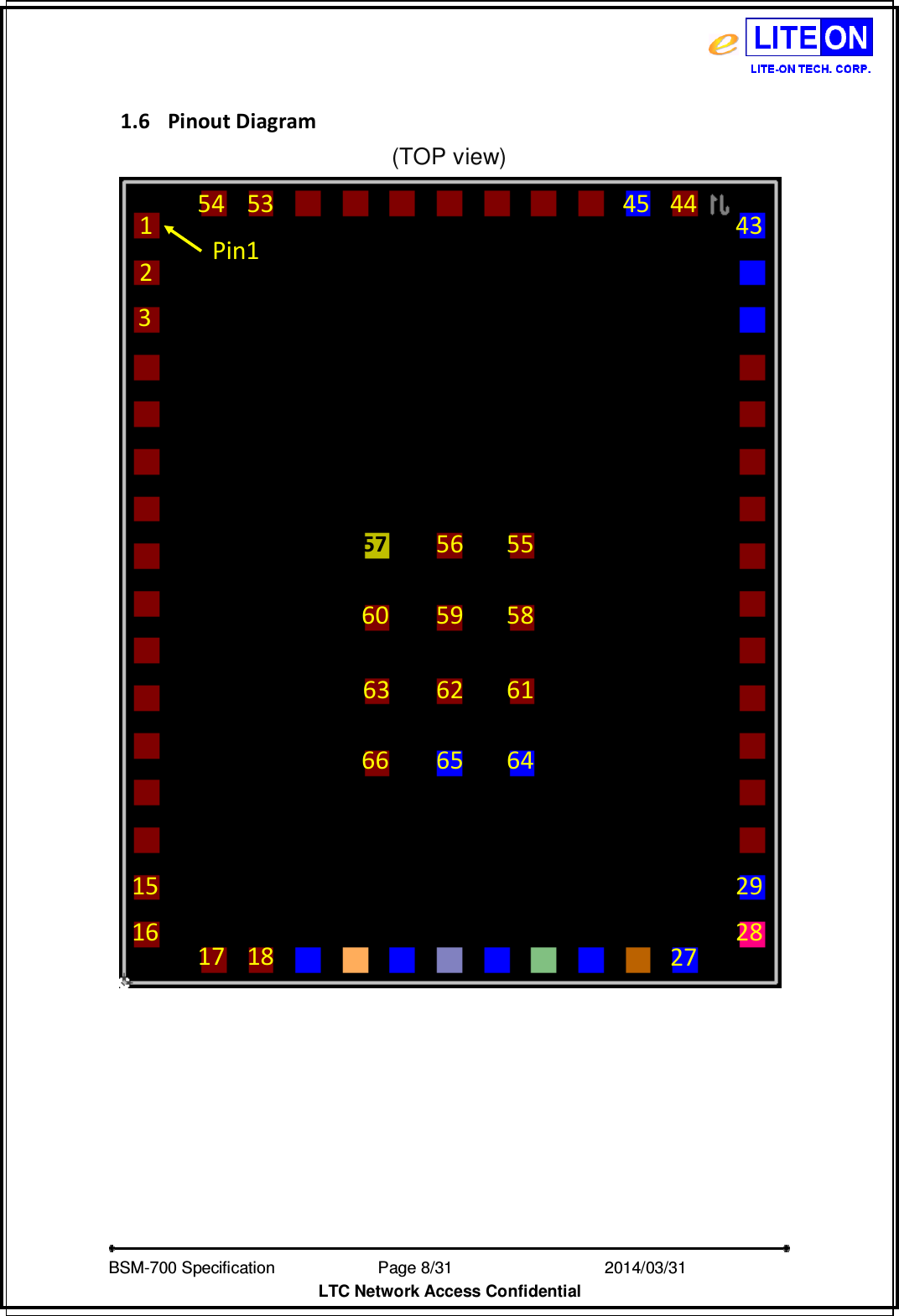
![BSM-700 Specification Page 6/31 2014/03/31 LTC Network Access Confidential 10 PIO_14 Programmable input / output line Bidirectional with weak pull-down 11 PIO_10 Programmable input / output line Bidirectional with weak pull-down 12 PIO_1 Programmable input / output line Bidirectional with weak pull-down 13 PIO_4 Programmable input / output line Bidirectional with weak pull-down 14 PIO_15 Programmable input / output line Bidirectional with weak pull-down 15 PIO_11 Programmable input / output line Bidirectional with weak pull-down 16 PIO_5 Programmable input / output line Bidirectional with weak pull-down 17 LED_1 LED driver[1] Open drain 18 PIO_7_I2C_SDA Programmable input / output line Bidirectional with weak pull-down 19 GND Ground 20 1V8 External 3.3V enable control Output 21 GND Ground 22 VDDIO Positive supply for I/O Power input 23 GND Ground 24 3V3 Positive supply for USB ports Power input 25 GND Ground 26 VBAT Battery positive terminal Power input 27 GND Ground 28 USB_5V Battery charger input Power input 29 GND Ground 30 VREGENABLE Regulator enable input for system on Input 31 MIC_IN_LN Microphone input negative, left Analogue in 32 MIC_IN_LP Microphone input positive, left Analogue in 33 MIC_BIAS_A Microphone bias A Analogue out 34 MIC_IN_RN Microphone input negative, right Analogue in 35 MIC_IN_RP Microphone input positive, right Analogue in 36 MIC_BIAS_B Microphone bias B Analogue out 37 BT_SPKR_RN Speaker output negative, right Analogue out 38 BT_SPKR_RP Speaker output positive, right Analogue out 39 BT_SPKR_LN Speaker output negative, left Analogue out 40 BT_SPKR_LP Speaker output positive, left Analogue out](https://usermanual.wiki/LITE-ON-TECHNOLOGY/BSM700/User-Guide-2266335-Page-6.png)
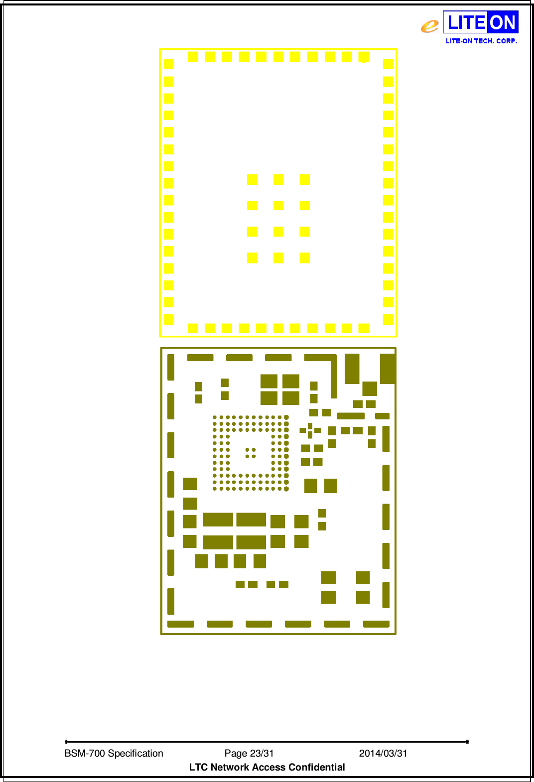
![BSM-700 Specification Page 7/31 2014/03/31 LTC Network Access Confidential 41 GND Ground 42 GND Ground 43 GND Ground 44 Antenna2 External Antenna with RF PAD RF PAD 45 GND Ground 46 SPI_CLK SPI clock Input with weak pull- Down 47 SPI_MOSI SPI data in Input with weak pull- Down 48 BT_I2S_IN I2S data in Bidirectional with weak pull-down 49 BT_I2S_BCLK I2S data clock Bidirectional with weak pull-down 50 BT_I2S_LRCLK I2S data sync Bidirectional with weak pull-down 51 BT_I2S_OUT I2S data out Bidirectional with weak pull-down 52 SPI_MISO SPI data out Output with weak pull- down 53 RST# Reset if low. Input de-bounced so must be low for >5ms to cause a reset. Input with strong pull-up 54 SPI_CS# Chip select for SPI, active low. Input with strong pull-up 55 FLASF_IO2 Serial quad I/O flash data bit 2 Alternative function PIO[27] Bidirectional with strong pull-down 56 FLASF_CS# SPI flash chip select. Alternative function PIO[23] Bidirectional with strong pull-down 57 AIO[0] Programmable input / output line Analogue programmable input / output line 58 FLASF_IO1 Serial quad I/O flash data bit 1. Alternative function PIO[26] Bidirectional with strong pull-down 59 FLASF_CLK SPI flash clock. Alternative function PIO[21] Bidirectional with strong pull-down 60 PIO_3 Programmable input / output line Bidirectional with weak pull-down 61 FLASF_IO0 Serial quad I/O flash data bit 0. Alternative function PIO[25] Bidirectional with strong pull-down 62 FLASF_IO3 Serial quad I/O flash data bit 3. Alternative function PIO[28] Bidirectional with strong pull-down 63 PIO_12 Programmable input / output line Bidirectional with weak pull-down 64 GND Ground 65 GND Ground 66 PIO_13 Programmable input / output line Bidirectional with weak pull-down](https://usermanual.wiki/LITE-ON-TECHNOLOGY/BSM700/User-Guide-2266335-Page-7.png)
![BSM-700 Specification Page 18/31 2014/03/31 LTC Network Access Confidential 5 Notes on operation 5.1 Power-on Sequence We recommend that the power supplies are all powered at the same time. 5.2 IO State at Reset and Recommended Termination Handling The RESET# pin is an active low reset. Assert the reset signal for a period >5ms to ensure a full reset. The RESET # pin is pulled down internally until the power on, then the pull switches to a strong pull up. Pin Name / Group I/O Type Full Chip Reset USB_DP Digital bidirectional N/A USB_DN Digital bidirectional N/A UART_RX Digital bidirectional with PU Strong PU UART_TX Digital bidirectional with PU Weak PU SPI_CS# Digital input with PU Strong PU SPI_CLK Digital input with PD Weak PD SPI_MISO Digital tristate output with PD Weak PU SPI_MOSI Digital input with PD Weak PD I2S_OUT Digital bidirectional with PD Weak PD I2S_SYNC Digital bidirectional with PD Weak PD I2S_BCLK Digital bidirectional with PD Weak PD RST# Digital input with PU Strong PU PIO[15:0] Digital bidirectional with PD Weak PD FLASH_IO[3:0] Digital bidirectional with PD Strong PD FLASH_CS# Digital bidirectional with PU Strong PU FLASH_CLK Digital bidirectional with PD Strong PD](https://usermanual.wiki/LITE-ON-TECHNOLOGY/BSM700/User-Guide-2266335-Page-18.png)