LITE ON TECHNOLOGY BSM700 Bluetooth Module User Manual BSM 700 BT4 0 Spec ver1 3
LITE-ON Technology Corp. Bluetooth Module BSM 700 BT4 0 Spec ver1 3
User manual

BSM-700 Specification Page 1/31 2014/03/31
LTC Network Access Confidential
PRODUCT SPECIFICATION
CSR8670 Full function Bluetooth Module
BSM-700
Lite-On P/N: 2170000002KD
Version 1.3
Author: Action Cheng Editor: Javon Tseng
Project Leader: Daniel KW Yang Approved by: Daniel KW Yang
Change History
Revision Date Author Change List
Version 1.0 2014 / 01 / 13 Javon Tseng Preliminary
Version1.1 2014 /01 / 24 Daniel
1.
Add pinout dimensions
2. Remove NC (Pin57) and connect
AIO[0] to PIN 57.
3. Remove PIO0 (Pin4) and connect
AIO[1] to PIN 4
4. Add PIO_3 to PIN60
Version1.2 2014 /02 / 06 Javon
1.
U
pdate Block Diagram
2. Update Application block diagram
3. Update main board schematic
Version1.3 2014 /04 / 03 Javon
1.
Add Packing Model
2. Update Current Consumption
3. Update Package Dimensions
4. Update RF Characteristics
5. Update Interface Specifications
6. Update Layout
* This document contains confidential proprietary information and is property of LTC. The contents of
this document should not be disclosed to unauthorized persons without the written consent of LTC.

BSM-700 Specification Page 2/31 2014/03/31
LTC Network Access Confidential
CONTENT
1 PRODUCT OVERVIEW ................................................................................................................. 4
1.1 DESCRIPTION ........................................................................................................................ 4
1.2 FEATURES ............................................................................................................................. 4
1.3 GENERAL SPECIFICATIONS ................................................................................................. 4
1.4 BLOCK DIAGRAM .................................................................................................................. 5
1.5 PIN CONFIGURATION............................................................................................................ 5
1.6 PINOUT DIAGRAM ................................................................................................................ 8
1.7 PACKAGE DIMENSIONS......................................................................................................... 9
1.8 DIMENSION ........................................................................................................................ 10
1.9 SHIELDING .......................................................................................................................... 11
2 ELECTRICAL CHARACTERISTICS ................................................................................................. 12
2.1 ABSOLUTE MAXIMUM RATINGS ......................................................................................... 12
2.2 GUARANTEED OPERATING TEMPERATURE ......................................................................... 12
2.3 RECOMMENDED OPERATING CONDITIONS ........................................................................ 12
2.4 INPUT/OUTPUT TERMINAL CHARACTERISTICS.................................................................... 12
2.5 RF CHARACTERISTICS .......................................................................................................... 13
2.5.1 RADIO CHARACTERISTICS - BASIC DATA RATE .................................................................... 13
2.5.2 RADIO CHARACTERISTICS - ENHANCED DATA RATE ............................................................ 13
2.5.3 RADIO CHARACTERISTICS - LOW ENERGY ........................................................................... 13
2.6 CURRENT CONSUMPTION (DESIGN REFERENCE) ................................................................. 13
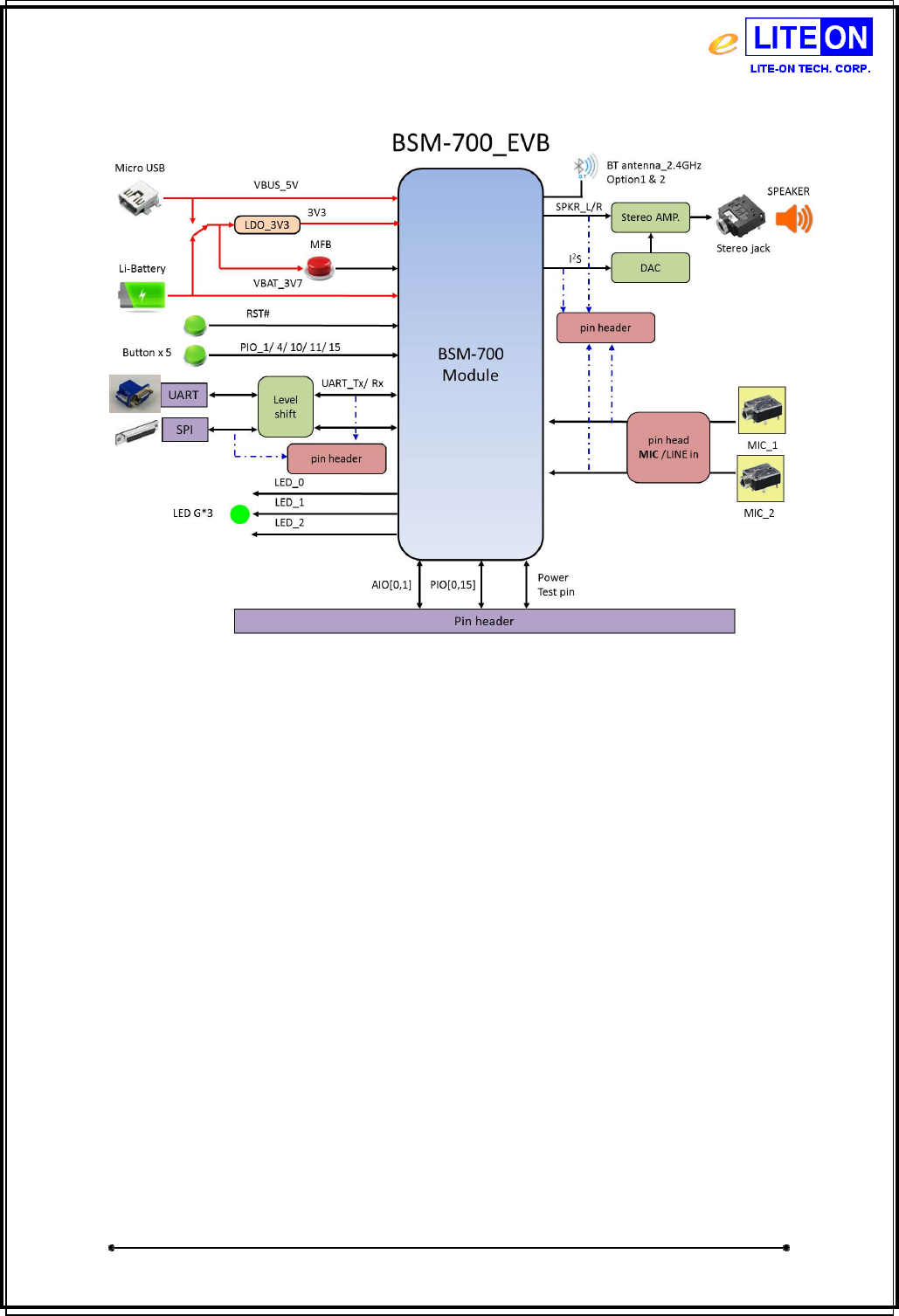
2.7 APPLICATION BLOCK DIAGRAM .......................................................................................... 14
3 RF MEASUREMENT ENVIRONMENT SYSTEM ............................................................................ 15
3.1 INTERNAL FLASH................................................................................................................. 15
3.2 SYSTEM AREA ..................................................................................................................... 15
3.3 RF AREA .............................................................................................................................. 16
3.4 USER AREA ......................................................................................................................... 16
4 INTERFACE SPECIFICATIONS ..................................................................................................... 17
4.1 UART INTERFACE ................................................................................................................ 17

BSM-700 Specification Page 3/31 2014/03/31
LTC Network Access Confidential
4.2 USB INTERFACE................................................................................................................... 17
4.3 DIGITAL AUDIO INTERFACE ................................................................................................. 17
5 NOTES ON OPERATION ............................................................................................................ 18
5.1 POWER-ON SEQUENCE ....................................................................................................... 18
5.2 IO STATE AT RESET AND RECOMMENDED TERMINATION HANDLING ................................. 18
6 SCHEMATIC .............................................................................................................................. 19
6.1 MAIN BLOCK: ...................................................................................................................... 19
6.2 RF ....................................................................................................................................... 20
7 PLACEMENT ............................................................................................................................. 20
8 LAYOUT .................................................................................................................................... 21
9 REFLOW CONDITION ................................................................................................................ 27
9.1 REFLOW TEMPERATURE PROFILE ....................................................................................... 27
10 MARKING AND PACKING MODEL ............................................................................................. 27
10.1 MARKING ........................................................................................................................... 27
10.2 PACKING MODEL ................................................................................................................ 28
11 CRITERIA FOR RELIABILITY TEST ............................................................................................... 29
12 FCC COMPLIANCE AND ADVISORY STATEMENT ....................................................................... 30
12.1 CLASS B: (SECTION 15.105) .............................................................................................. 30
12.2 LABELING REQUIREMENTS ................................................................................................. 30
12.3 RF EXPOSURE WARNING .................................................................................................... 30
12.4 END PRODUCT LABELING .................................................................................................... 31
BSM-700 Specification Page 4/31 2014/03/31
LTC Network Access Confidential
1 Product Overview
1.1 Description
BSM-700 is a LGA type Bluetooth module which using CSR Chipset CSR8670C‑IBBH‑R
1.2 Features
Bluetooth® v4.0 specification fully qualified software
Radio includes integrated balun
Class II (Max +4 dBm, 2.5mW)
High-sensitivity Bluetooth receiver
16Mb internal flash memory (64-bit wide,45ns)
Integrated 16-bit Stereo Audio CODEC
Embedded Kalimba DSP Co-Processor.
Support for CSR's latest CVC technology for narrow-band and wideband voice
connections including wind noise reduction
Audio interfaces: I²S, PCM and SPDIF
Serial interfaces: UART, USB 2.0 full-speed, I²C
Integrated dual switch-mode regulators, linear regulators and battery charger
3 hardware LED controllers (for RGB) and ability to drive LCD segment display directly
Green (RoHS compliant and no antimony or halogenated flame retardants)
1.3 General Specifications
Standard Bluetooth v3.0 EDR, 4.0 LE Compliant.
Bus Interface
Data:
UART
/ USB
Voice: PCM/I2S/Stereo Analog in/out
Form Factor
22mm x 18mm x 2.5mm
LGA (Land Grid Array) pads reliable PCB mounting.
Data Rate 1 Mbps, 2Mbps and Up to 3Mbps
Frequency Range 2.402 ~ 2.480 GHz
Transmit Output Power
-6 ~ +4 dBm Class 2 Device
Receive Sensitivity BER < 0.1% BER at -80 dBm
Operating Voltage 3.1V~3.6V I/O supply voltage
Antenna Type Option1:I-pex connector Option2:Feed point
BSM-700 Specification Page 5/31 2014/03/31
LTC Network Access Confidential
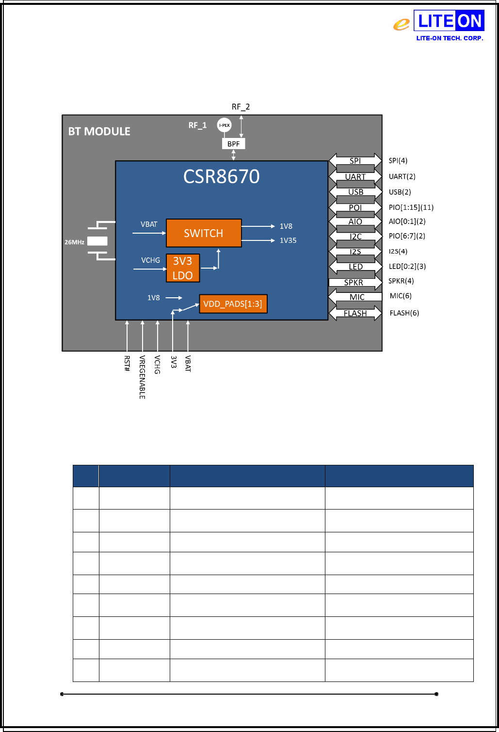
1.4 Block Diagram
1.5 Pin Configuration
No Definition Description Type
1 UART_RX UART data in
Bidirectional with strong
pull-up
2 UART_TX UART data output
Bidirectional with weak
pull-up
3 LED_0 LED driver[0] Open drain
4 AUO[1] Programmable input / output line
Analogue
programmable input /
output line
5 LED_2 LED driver[2] Open drain
6 PIO_6_I2C_SCK Programmable input / output line
Bidirectional with weak
pull-down
7 USB_D+
USB data plus with selectable internal
1.5kΩ pull-up resistor Bidirectional
8 USB_D- USB data minus Bidirectional
9 PIO_2 Programmable input / output line
Bidirectional with weak
pull-down
BSM-700 Specification Page 6/31 2014/03/31
LTC Network Access Confidential
10 PIO_14 Programmable input / output line
Bidirectional with weak
pull-down
11 PIO_10 Programmable input / output line
Bidirectional with weak
pull-down
12 PIO_1 Programmable input / output line
Bidirectional with weak
pull-down
13 PIO_4 Programmable input / output line
Bidirectional with weak
pull-down
14 PIO_15 Programmable input / output line
Bidire
ctional with weak
pull-down
15 PIO_11 Programmable input / output line
Bidirectional with weak
pull-down
16 PIO_5 Programmable input / output line
Bidirectional with weak
pull-down
17 LED_1 LED driver[1] Open drain
18 PIO_7_I2C_SDA
Programmable input / output line
Bidirectional with weak
pull-down
19 GND Ground
20 1V8 External 3.3V enable control Output
21 GND Ground
22 VDDIO Positive supply for I/O Power input
23 GND Ground
24 3V3 Positive supply for USB ports Power input
25 GND Ground
26 VBAT Battery positive terminal Power input
27 GND Ground
28 USB_5V Battery charger input Power input
29 GND Ground
30 VREGENABLE Regulator enable input for system on Input
31 MIC_IN_LN Microphone input negative, left Analogue in
32 MIC_IN_LP Microphone input positive, left Analogue in
33 MIC_BIAS_A Microphone bias A Analogue out
34 MIC_IN_RN Microphone input negative, right Analogue in
35 MIC_IN_RP Microphone input positive, right Analogue in
36 MIC_BIAS_B Microphone bias B Analogue out
37 BT_SPKR_RN Speaker output negative, right Analogue out
38 BT_SPKR_RP Speaker output positive, right Analogue out
39 BT_SPKR_LN Speaker output negative, left Analogue out
40 BT_SPKR_LP Speaker output positive, left Analogue out
BSM-700 Specification Page 7/31 2014/03/31
LTC Network Access Confidential
41 GND Ground
42 GND Ground
43 GND Ground
44 Antenna2 External Antenna with RF PAD RF PAD
45 GND Ground
46 SPI_CLK SPI clock
Input with weak pull
-
Down
47 SPI_MOSI SPI data in
Input with weak pull
-
Down
48 BT_I2S_IN I2S data in
Bidirectional with weak
pull-down
49 BT_I2S_BCLK I2S data clock
Bidirectional with weak
pull-down
50 BT_I2S_LRCLK I2S data sync
Bidirectional with weak
pull-down
51 BT_I2S_OUT I2S data out
Bidirectional with weak
pull-down
52 SPI_MISO SPI data out
Output with weak pull
-
down
53 RST#
Reset if low.
Input de
-
bounced so must
be low for >5ms to cause a reset. Input with strong pull-up
54 SPI_CS# Chip select for SPI, active low. Input with strong pull-up
55 FLASF_IO2
Serial quad I/O flash data bit 2
Alternative function PIO[27]
Bidirectional with stron
g
pull-down
56 FLASF_CS#
SPI flash chip select.
Alternative function PIO[23]
Bidirectional with strong
pull-down
57 AIO[0] Programmable input / output line
Analogue programmable input /
output line
58 FLASF_IO1
Serial quad I/O flash data bit 1.
Alternative function PIO[26]
Bidirectional with strong
pull-down
59 FLASF_CLK
SPI flash clock.
Alternative function PIO[21]
Bidirectional with strong
pull-down
60 PIO_3 Programmable input / output line
Bidirectional with weak
pull-down
61 FLASF_IO0
Serial quad
I/O flash data bit 0.
Alternative function PIO[25]
Bidirectional with strong
pull-down
62 FLASF_IO3
Serial quad I/O flash data bit 3.
Alternative function PIO[28]
Bidirectional with strong
pull-down
63 PIO_12 Programmable input / output line
Bidirectiona
l with weak
pull-down
64 GND Ground
65 GND Ground
66 PIO_13 Programmable input / output line
Bidirectional with weak
pull-down
BSM-700 Specification Page 8/31 2014/03/31
LTC Network Access Confidential
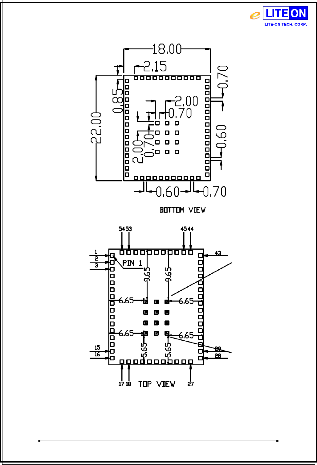
1.6 Pinout Diagram
(TOP view)
1
2
3
16
15
17 18 27
28
43
4445
54 53
5556
6566
Pin1
57
585960
616263
64
29
BSM-700 Specification Page 9/31 2014/03/31
LTC Network Access Confidential
1.7 Package Dimensions
BSM-700 Specification Page 10/31 2014/03/31
LTC Network Access Confidential
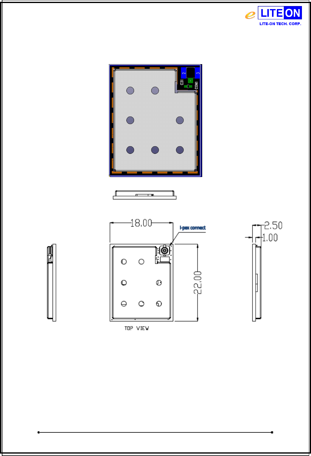
1.8 Dimension
Dimension of BSM-700 : 22 x 18 x 2.5mm
BSM-700 Specification Page 11/31 2014/03/31
LTC Network Access Confidential
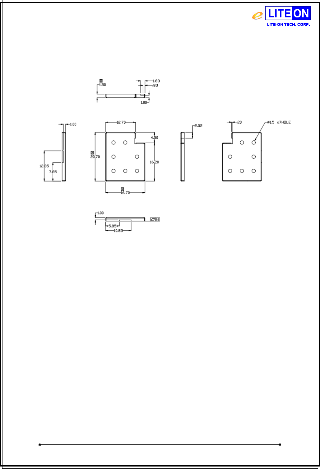
1.9 Shielding
Dimension of shielding : 20.7 x 16.7 x 1.5mm
Hole : 1.5mm
BSM-700 Specification Page 12/31 2014/03/31
LTC Network Access Confidential
2 Electrical Characteristics
2.1 Absolute Maximum Ratings
Rating
Min
Max
Unit
USB_5V
-
0.4
0
5.75
V
VBAT -0.40 4.40 V
3V3
-
0.4
0
3.60
V
VDDIO
-
0.4
0
3.60
V
2.2 Guaranteed Operating Temperature
Operating
Operating Temperature: -40 to 85 °C
Storage
Temperature: -40 to 105 °C
2.3 Recommended Operating Conditions
Rating Min TYP Max Unit
USB_5V
4.75
5.00
5.75
V
VBAT
2.80
3.70
4.30
V
3V3
3.10
3.30
3.60
V
VDDIO
3.10
3.30
3.60
V
1V8 1.70 1.80 1.95 V
1V35
1.30
1.35
1.40
V
2.4 Input/Output Terminal Characteristics
Rating
Min
TYP
Max
Unit
VIL input logic level low
-
0.4
-
0.4
V
VIH input logic level high 0.7xVDDIO - VDDIO+0.4 V
VOL output logic level low,
lOL = 4.0mA
-
-
0.4
V
VOH output logic level
high, lOH = -4.0mA
0.75xVDDIO - 3.60 V
BSM-700 Specification Page 13/31 2014/03/31
LTC Network Access Confidential
2.5 RF Characteristics
2.5.1 Radio Characteristics - Basic Data Rate
RF Characteristics
Bluetooth Specification with
Unit
I
-
PEX
SMA
Maximum RF transmit power
-
6 to 4
-
6 to 4
dBm
Sensitivity at 0.1% BER TYP. -80dB TYP. -80dB dBm
2.5.2 Radio Characteristics - Enhanced Data Rate
RF Characteristics Bluetooth Specification with Unit
I
-
PEX
SMA
Sensitivity at 0.01% BER
TYP.
-
80dB
TYP.
-
80dB
dBm
2.5.3 Radio Characteristics - Low Energy
RF Characteristics
Bluetooth Specification with
U
nit
I
-
PEX
SMA
Sensitivity at 30.8% BER
TYP.
-
80dB
TYP.
-
80dB
dBm
2.6 Current Consumption (Design reference)
Mode Max. Avg. Min Unit
Idle 0.465 0.183 0.054 mA
ACL 8.940 0.482 0.057 mA
SOC 16.0 13.0 12.3 mA
eSOC 14.6 12.7 12.4 mA
BSM-700 Specification Page 14/31 2014/03/31
LTC Network Access Confidential
2.7 Application block diagram
BSM-700 Specification Page 15/31 2014/03/31
LTC Network Access Confidential
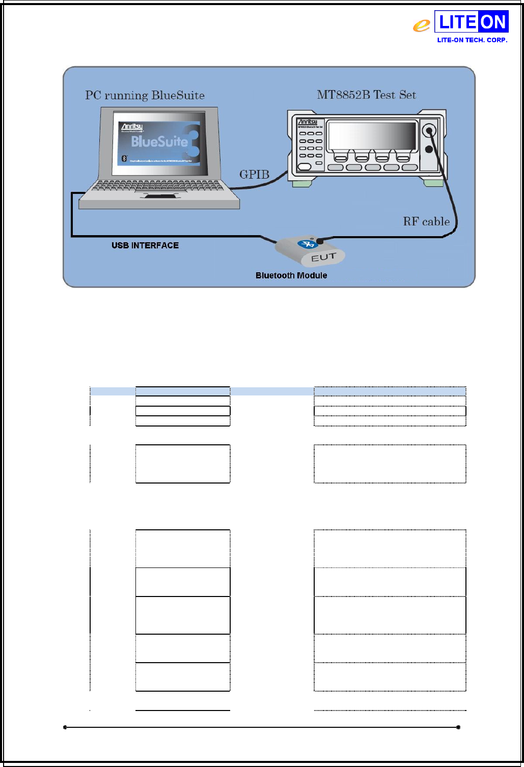
3 RF Measurement Environment System
3.1 Internal Flash
PSR and File System for MP build: V0.2
3.2 System Area
Index
Name
Description
Value
0x01EA
UART_BITRATE Baud Rate delete or "0"
0x01F9 HOST_INTERFACE Host I/F Configuration 0001 (UART link running BCSP)
0x0246 CLOCK_REQUEST_ENABLE delete
0x212C PATCH50 0000 C47D 5714 0018 FF2B FF0E D800 7918
009E 0018 FF2B FF0E C500 8018 00E2 7080
0x212D PATCH51
0002 5B79 0014 E700 9525 011B 0626 089A
0AF4 0218 FF2B FF0E 5B00 4318 009E 0014
011B 0826 0218 FF2B FF0E 5C00 8218 00E2
A63A
0x212E PATCH52
0002 D0A7 0316 0318 FF2B FF0E 2300 0618
009E E199 14F4 E119 0812 8000 00C0 10F0
061B 0212 0100 FFC0 0780 0AF0 0316 0010
0318 FF2B FF0E 3800 1318 009E F70F 0218
FF2B FF0E D100 AC18 00E2 CF53
0x212F PATCH53
0003 C916 0114 0027 0517 2B00 A484 06F0
2B00 A914 0527 0114 02E0 0014 0127 0014
0227 0323 E315 0318 FF2B FF0E C900 1D18
00E2 CB5F
0x2130 PATCH54
0002 CA7A 0018 FF2B FF0E 8400 CB18 009E
EA00 5F11 0100 0080 0524 0100 00B0 EA00
5F21 0218 FF2B FF0E CA00 7D18 0
0E2 2513
0x2131 PATCH55
0003 FE75 EB00 C114 0218 FF2B FF0E 6700
E718 009E EA00 6714 0218 FF2B FF0E 6700
E718 009E 0318 FF2B FF0E FE00 7A18 00E2
0C6F
0x2134 PATCH58
0001 1A6F 051B 0116 0284 03F0 0310 0122
0110 071B 0100 8922 0118 FF2B FF0E 1A00
7318 00E2 D58C
0x2135 PATCH59
0001 14D1 FF40 0627 0523 091B 0116 0284
07F0 0310 0122 5F16 4800 00B4 5F26 0118
FF2B FF0E 1500 D418 00E2 F7FE
0x212F PATCH60 0003 F9A5 0318 FF2B FF0E F900 F018 009E
E199 04F4 4000 FF14 F90F 0318 FF2B FF0E
BSM-700 Specification Page 16/31 2014/03/31
LTC Network Access Confidential
F900 7318 00E2 AEC3
0x21FB PATCH107
F000 3215 0800 00B4 F000 3225 F000 3215
F800 FFC4 F000 3225 F000 3215 0800 00B4
F000 3225 00E2 49E0
0x2200
PATCH112
F100 CF15 01B4 F100 CF25 00E2 9DD1
3.3 RF Area
Index Name Description Value
0x0017 LC_MAX_TX_POWER Maximum Tx
power
0000 (0dBm)
0x003C RX_MR_SAMP_CONFIG 0426
0x216D BT_MIXER_CTRIM_CHAN0_MAX 0007
0x2175 BT_TX_MIXER_CTRIM_OFFSET 1111 0000 0000 0000 fff0
0x241A BT_POWER_TABLE_V0 2217 0050 2c48 0050 ec00
2417 0040 2e48 0040 f000
2317 0030 2d48 0030 f400
2317 0020 2d48 0020 f800
2417 0010 2d48 0010 fc00
2717 0000 3049 0000 0000
0x03DA TEMPERATURE_VS_DELTA_INTERNAL
_PA
ffec 0001 0019 0000 004b 000a
0x21E1 TEMPERATURE_VS_DELTA_INTERNAL
_PA_MR
ffec ffff 0019 0000 004b 0007
3.4 User Area
Index Name Description Value
0x267 MOD_MANUF9 Serial Number and
Hardware Version
YYMMDDLLSSSSHH
YY : Year (0C => 2012)
MM : Month (range : 01 - 0C)
DD : Date (range : 01 - 1F)
LL : Line Number (range : 01 - FF)
SSSS : Serial Number (range : 0001 - FFFF)
HH : Hardware (04 : MP)
BSM-700 Specification Page 17/31 2014/03/31
LTC Network Access Confidential
4 Interface Specifications
4.1 UART Interface
Parameter
Possible Values
Baud rate Minimum
1200 baud (≤2%Error)
9600 baud (≤1%Error)
Maximum
4M baud (≤1%Error)
Parity None, Odd or Even
Number of stop bits
1 or 2
Bits per byte
8
4.2 USB Interface
BSM-700 has a full-speed (12Mbps) USB interface for communicating with other compatible digital devices.
The USB interface on BSM-700 acts as a USB peripheral, responding to requests from a master host
controller.BSM-700 supports the Universal Serial Bus Specification, Revision v2.0 (USB v2.0 Specification)
4.3 Digital Audio Interface
The audio PCM interface on the BSM-700 supports:
On-chip routing to Kalimba DSP
Continuous transmission and reception of PCM encoded audio data over Bluetooth.
Processor overhead reduction through hardware support for continual transmission and reception of PCM
data.
A bidirectional digital audio interface that routes directly into the baseband layer of the firmware.
Hardware on BSM-700 for sending data to and from a SCO connection.
PCM interface master, generating PCM_SYNC and PCM_CLK.
PCM interface slave, accepting externally generated PCM_SYNC and PCM_CLK.
Various clock formats including:
Long Frame Sync
Short Frame Sync
GCI timing environments
13-bit or 16-bit linear, 8-bit μ-law or A-law companded sample formats.
Receives and transmits on any selection of 3 of the first 4 slots following PCM_SYNC.
BSM-700 Specification Page 18/31 2014/03/31
LTC Network Access Confidential
5 Notes on operation
5.1 Power-on Sequence
We recommend that the power supplies are all powered at the same time.
5.2 IO State at Reset and Recommended Termination Handling
The RESET# pin is an active low reset. Assert the reset signal for a period >5ms to ensure a full reset. The RESET
# pin is pulled down internally until the power on, then the pull switches to a strong pull up.
Pin Name / Group
I/O Type
Full Chip Reset
USB_DP
Digital bidirectional
N/A
USB_DN
Digital bidirectional
N/A
UART_RX
Digital bidirectional with PU
Strong PU
UART_TX Digital bidirectional with PU Weak PU
SPI_CS#
Digital input with
PU
Strong PU
SPI_CLK
Digital input with PD
Weak PD
SPI_MISO
Digital tristate output with PD
Weak PU
SPI_MOSI
Digital input with PD
Weak PD
I2S_OUT Digital bidirectional with PD Weak PD
I2S_SYNC
Digital bidirectional with PD
Weak PD
I2S_BCLK
Digital b
idirectional with PD
Weak PD
RST#
Digital input with PU
Strong PU
PIO[15:0]
Digital bidirectional with PD
Weak PD
FLASH_IO[3:0]
Digital bidirectional with PD
Strong PD
FLASH_CS#
Digital bidirectional with PU
Strong PU
FLASH_CLK
Digital bidirectional w
ith PD
Strong PD
BSM-700 Specification Page 19/31 2014/03/31
LTC Network Access Confidential
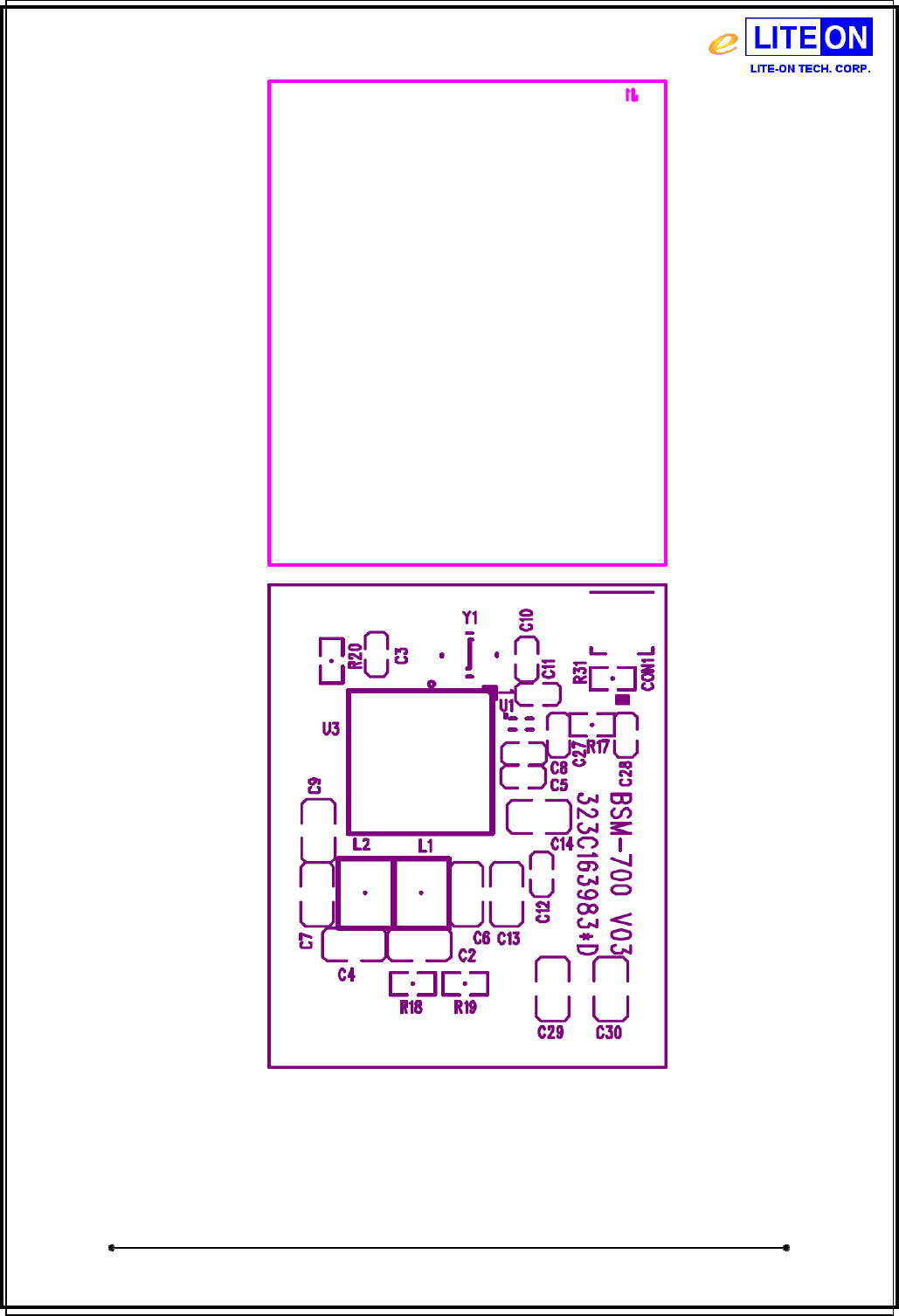
6 Schematic
6.1 Main Block:
BSM-700 Specification Page 20/31 2014/03/31
LTC Network Access Confidential
6.2 RF
7 Placement
No.
Function
Ref
1
Bluetooth Main
IC
U3
2 X’tal 26MHz Y1
3
Band Pass Filter
U1
BSM-700 Specification Page 21/31 2014/03/31
LTC Network Access Confidential
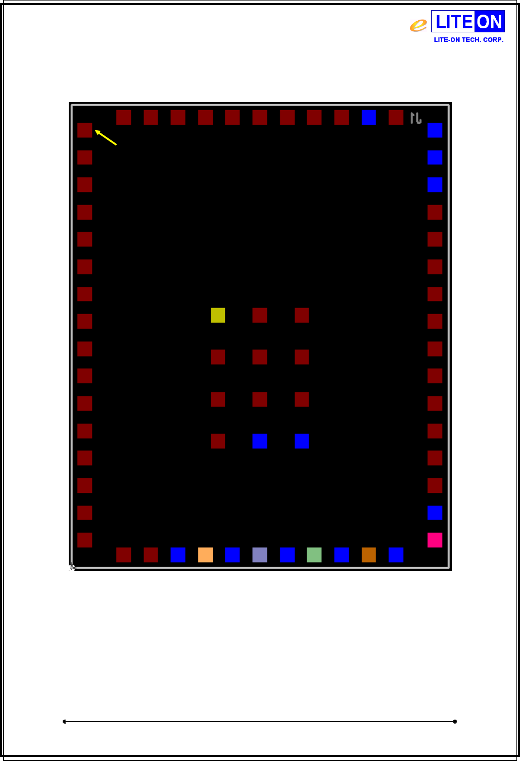
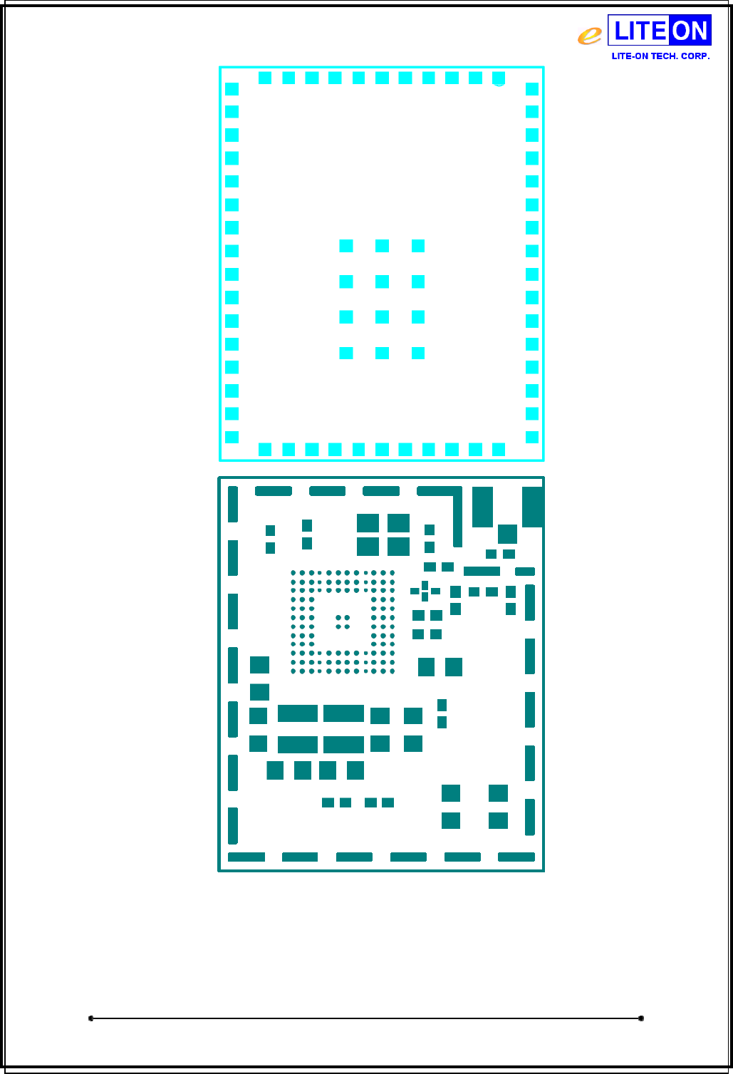
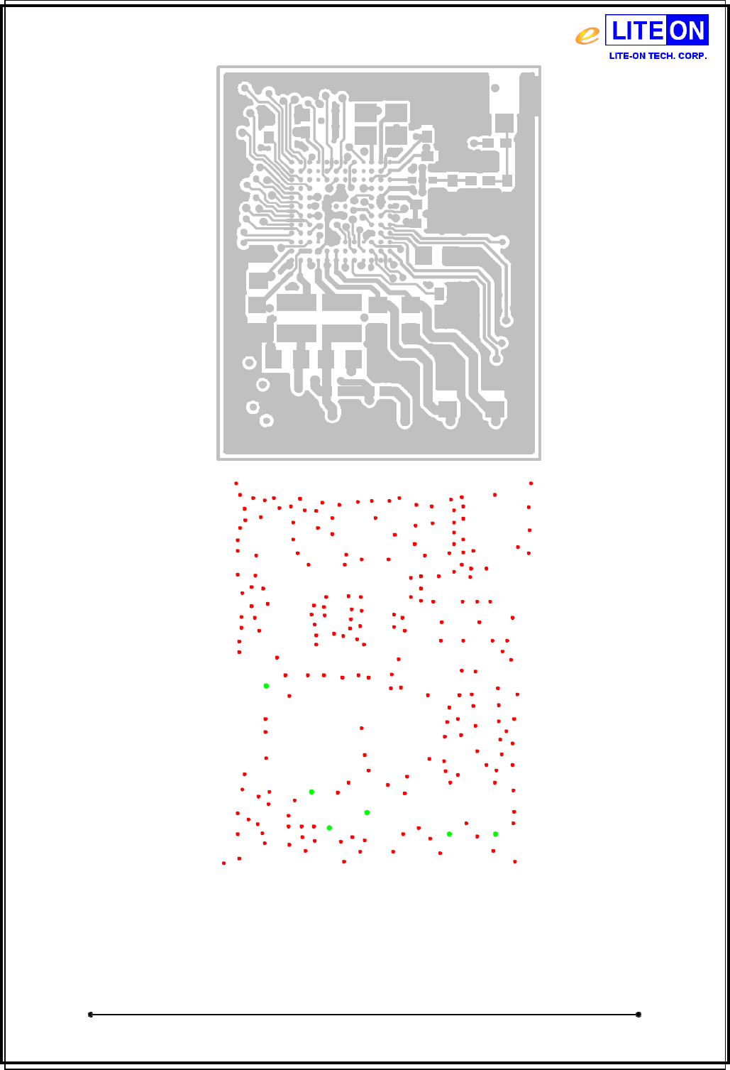
8 Layout
BSM-700 Specification Page 22/31 2014/03/31
LTC Network Access Confidential
BSM-700 Specification Page 23/31 2014/03/31
LTC Network Access Confidential
BSM-700 Specification Page 24/31 2014/03/31
LTC Network Access Confidential
BSM-700 Specification Page 25/31 2014/03/31
LTC Network Access Confidential
BSM-700 Specification Page 26/31 2014/03/31
LTC Network Access Confidential
BSM-700 Specification Page 27/31 2014/03/31
LTC Network Access Confidential
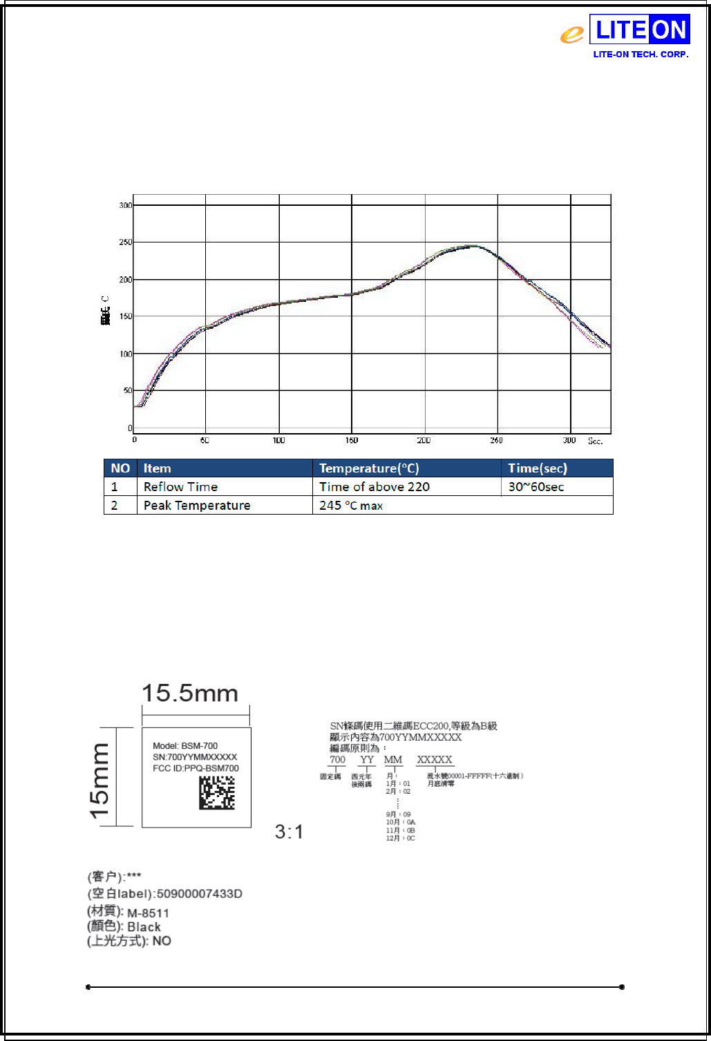
9 Reflow Condition
9.1 Reflow temperature profile
10 Marking and Packing Model
10.1 Marking
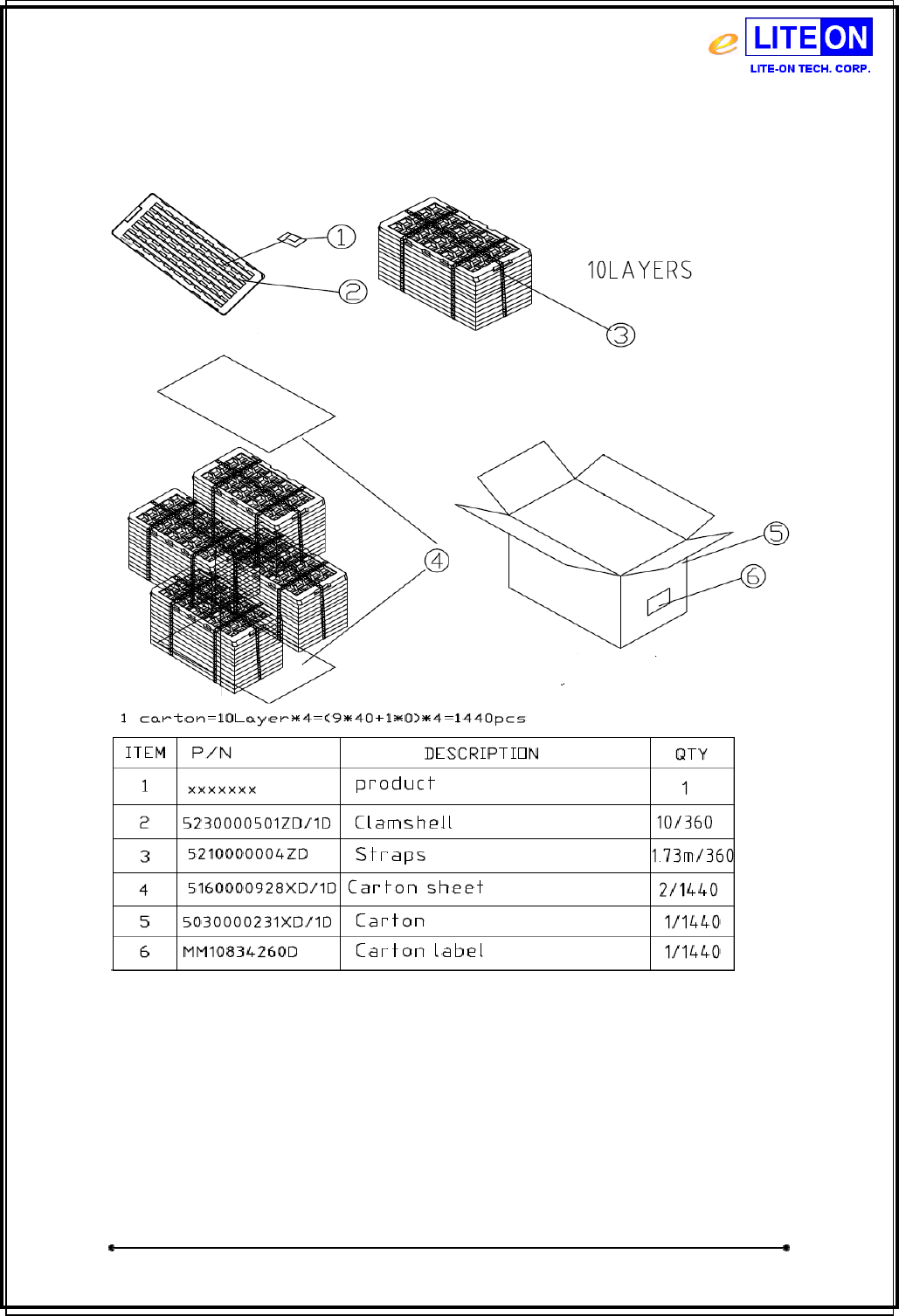
BSM-700 Specification Page 28/31 2014/03/31
LTC Network Access Confidential
10.2 Packing Model
BSM-700 Specification Page 29/31 2014/03/31
LTC Network Access Confidential
11 Criteria for Reliability Test
No.
Item
Condition
Unit
1
High Temperature High Humidity
Storage Test
1. Temperature/Humidity: 75
℃
±2
℃
95%±3RH
2. Test Time: 24Hrs
10pcs
2
Low Temperature Storage Test
1. Temperature:
-
40
℃
±2
℃
2. Test Time: 24Hrs
10pcs
3
3.1 Thermal Shock Test
1. High Temperature: 85
℃
15mins
2. Low Temperature: -40℃ 15mins
3. Temperature Rate: 25℃/Min
4. Duration: 200cycles
4pcs
3.1
-
1 X
-
Section Analysis
1. Environment: 21
℃
50%RH
2. Test location: ANT1, U2, XTAL1, U5
2pcs
4
Temperature Profile Test
1. Temperature: 70
℃
& 25
℃
2. Test Time: 6Hrs/Temp
3. Ping IP test
4. Test location: U2, U5, XTAL1,
2pcs
5
Operationa
l With Temperature Cycle Test
1. High Temperature/Humidity: 70
℃
90%RH 1H
2. Low Temperature: 0℃ 1H
3. Raise Time: 2℃/min Descend Time: 1℃/min
4. Duration: 10Cycles
2pcs
6
Power Cycling Test
1. Test Temperature/Humidity: 70
℃
90%RH 24Hrs &
25℃ 50%RH 24Hrs
2. Fixture: Power on 29mins & Power off 1min
3. Duration: 0.5H/Cycle ,Total 48Cycles
2pcs
7
Vibration Test
1. Vibration Wave: sine
2. Vibration Frequency: 10-300-10HZ 1G
3. Vibration Axis: Z Axis
4. Test time: 1Hr
2pcs

BSM-700 Specification Page 30/31 2014/03/31
LTC Network Access Confidential
12 FCC Compliance and Advisory Statement
12.1 Class B: (Section 15.105)
FEDERAL COMMUNICATIONS COMMISSION INTERFERENCE STATEMENT
This equipment has been tested and found to comply with the limits for a Class B
digital device, pursuant to part 15 of the FCC Rules. These limits are designed to
provide reasonable protection against harmful interference in a residential
installation. This equipment generates, uses and can radiate radio frequency energy
and, if not installed and used in accordance with the instructions, may cause harmful
interference to radio communications. However, there is no guarantee that
interference will not occur in a particular installation. If this equipment does cause
harmful interference to radio or television reception, which can be determined by
turning the equipment off and on, the user is encouraged to try to correct the
interference by one or more of the following measures:
-Reorient or relocate the receiving antenna.
-Increase the separation between the equipment and receiver.
-Connect the equipment into an outlet on a circuit different from that to which the
receiver is connected.
-Consult the dealer or an experienced radio/ TV technician for help.
CAUTION: (Section 15.21)
Any changes or modifications not expressly approved by the grantee of this device
could void the user's authority to operate the equipment.
12.2 Labeling requirements
This device complies with Part 15 of the FCC Rules. Operation is subject to the
following two conditions: (1) this device may not cause harmful interference, and (2)
this device must accept any interference received, including interference that may
cause undesired operation.
12.3 RF exposure warning
This equipment must be installed and operated in accordance with provided
instructions and the antenna(s) used for this transmitter must be installed to provide
a separation distance of at least 20 cm from all persons and must not be co-located
or operating in conjunction with any other antenna or transmitter. End-users and
installers must be provide with antenna installation instructions and transmitter
operating conditions for satisfying RF exposure compliance.

BSM-700 Specification Page 31/31 2014/03/31
LTC Network Access Confidential
12.4 End Product Labeling
This transmitter module is authorized only for use in device where the antenna may
be installed such that 20cm may be maintained between the antenna and users. The
final end product must be labeled in a visible area with the following: "Contains FCC
ID: PPQ-BSM700”
Information for the OEMs and Integrators
The following statement must be included with all versions of this document supplied
to an OEM or integrator, but should not be distributed to the end user.
1) This device is intended for OEM integrators only.
2) Please see the full Grant of Equipment document for other restrictions.
This radio transmitter FCC ID: PPQ-BSM700 has been approved by FCC to operate with the
antenna types listed below with the maximum permissible gain and required antenna
impedance for each antenna type indicated. Antenna types not included in this list, having a
gain greater than the maximum gain indicated for that type, are strictly prohibited for use
with this device.