LITE ON TECHNOLOGY CX8703BD120 JukeBlox Networked Media Module User Manual
LITE-ON Technology Corp. JukeBlox Networked Media Module
UserManual.wiki
>
LITE ON TECHNOLOGY
>
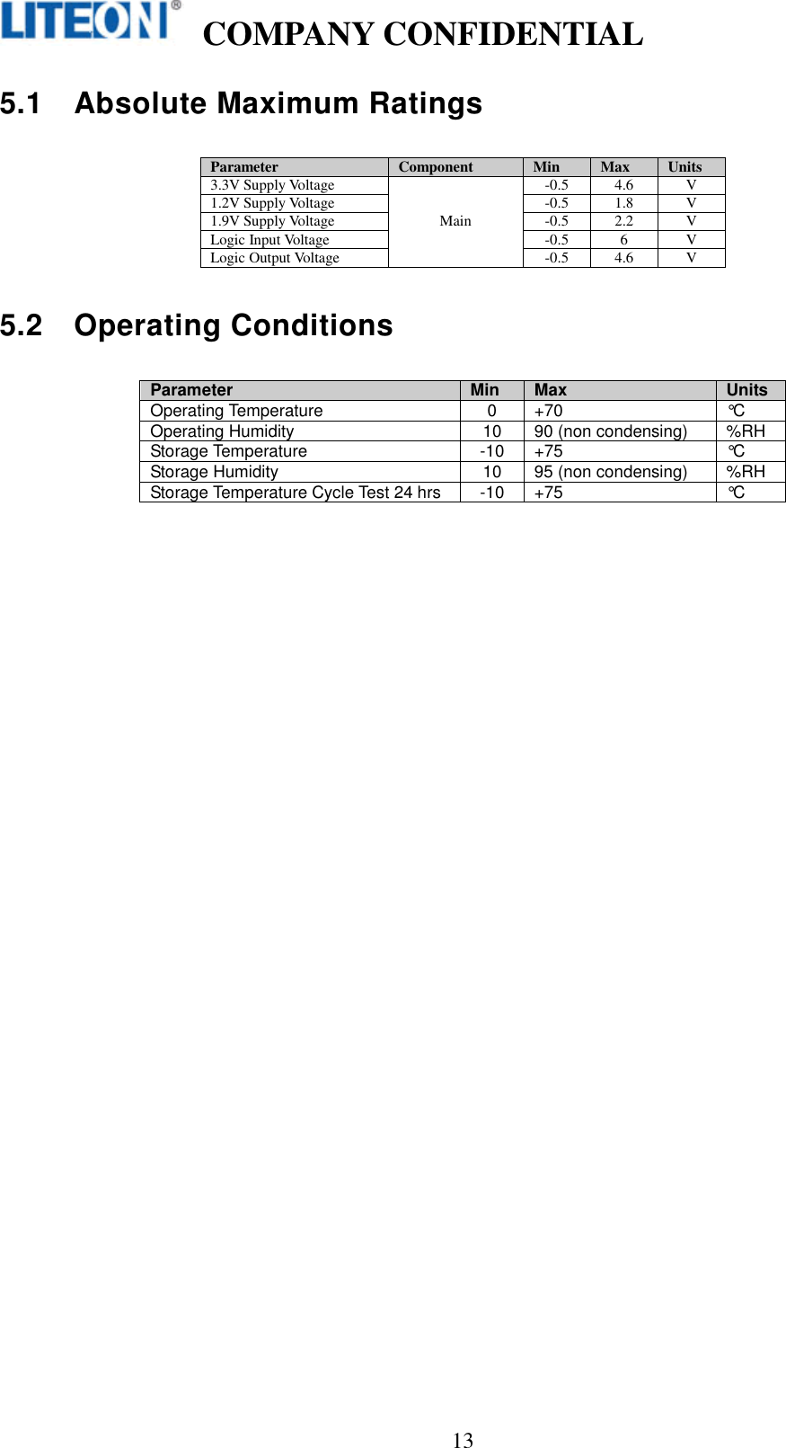
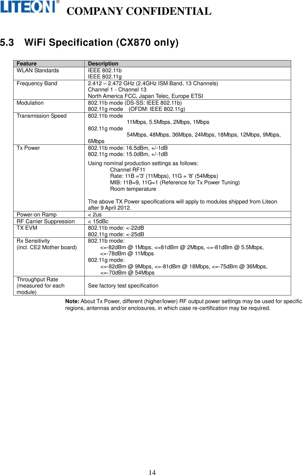
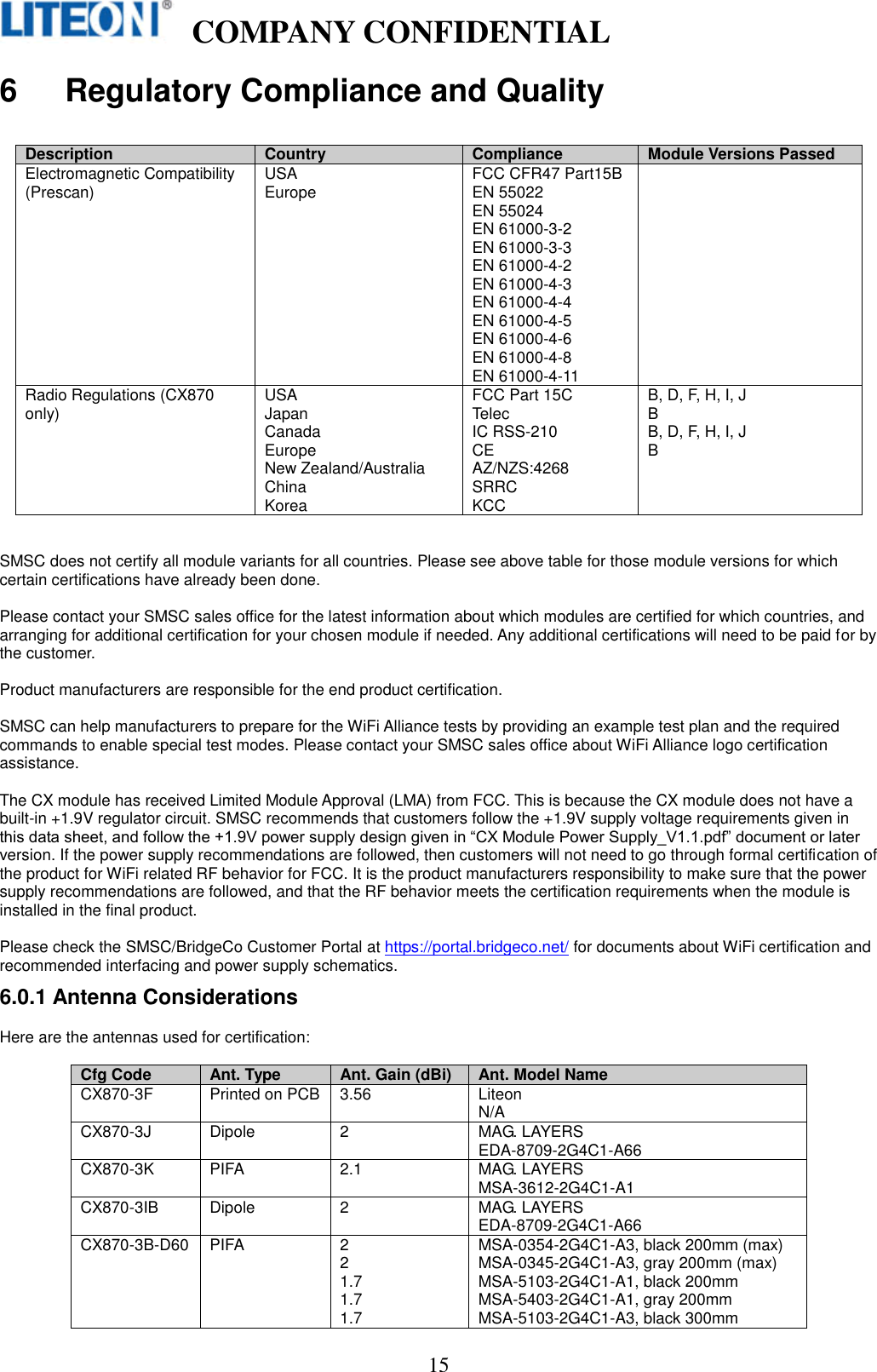
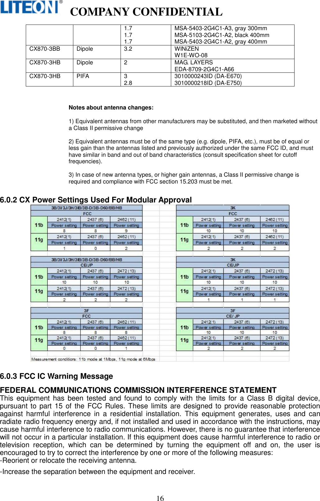
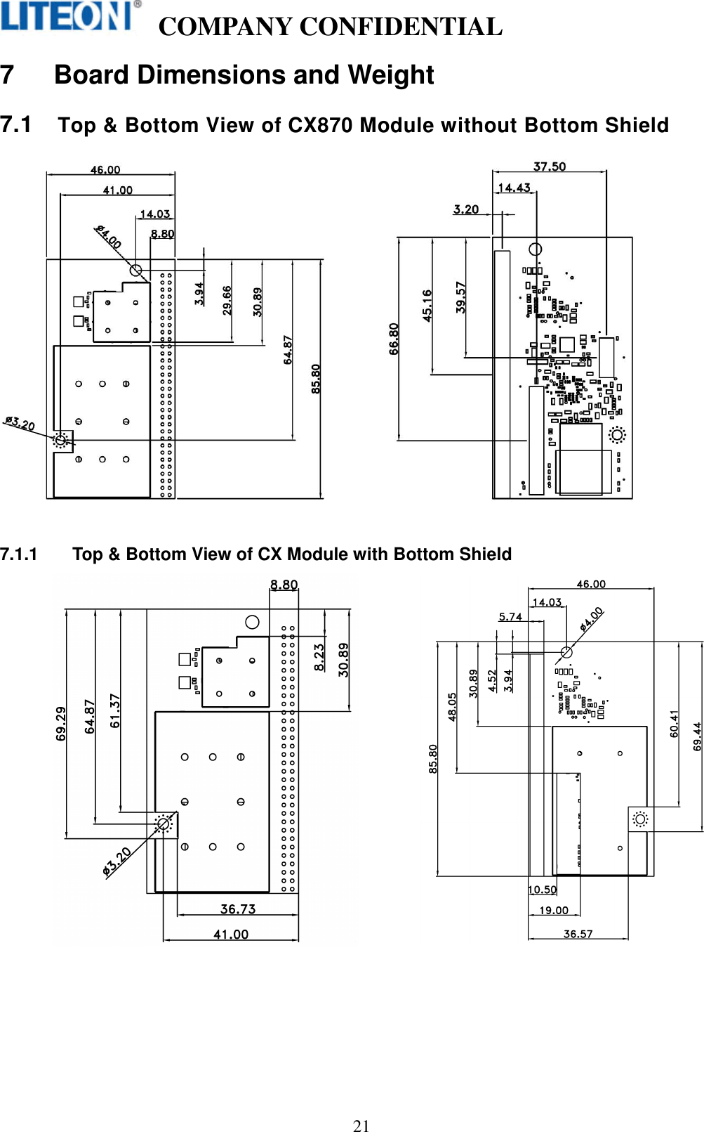
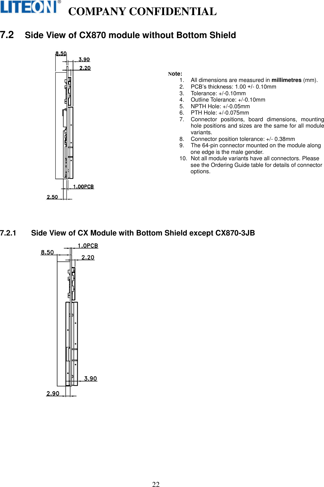
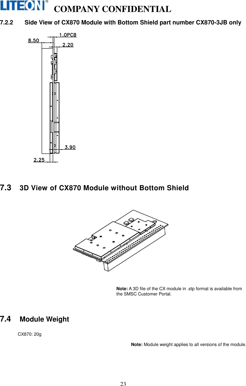
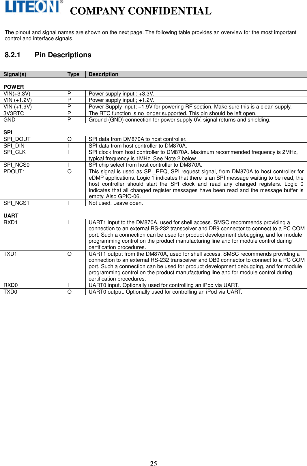
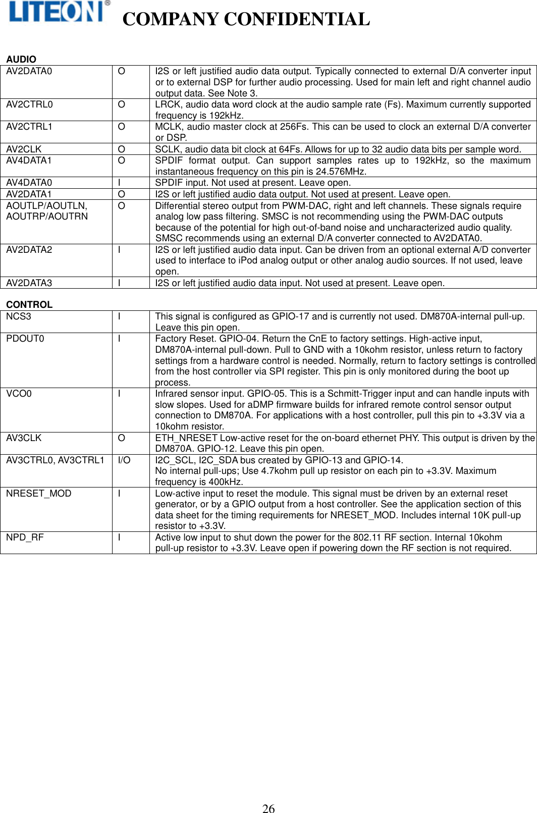
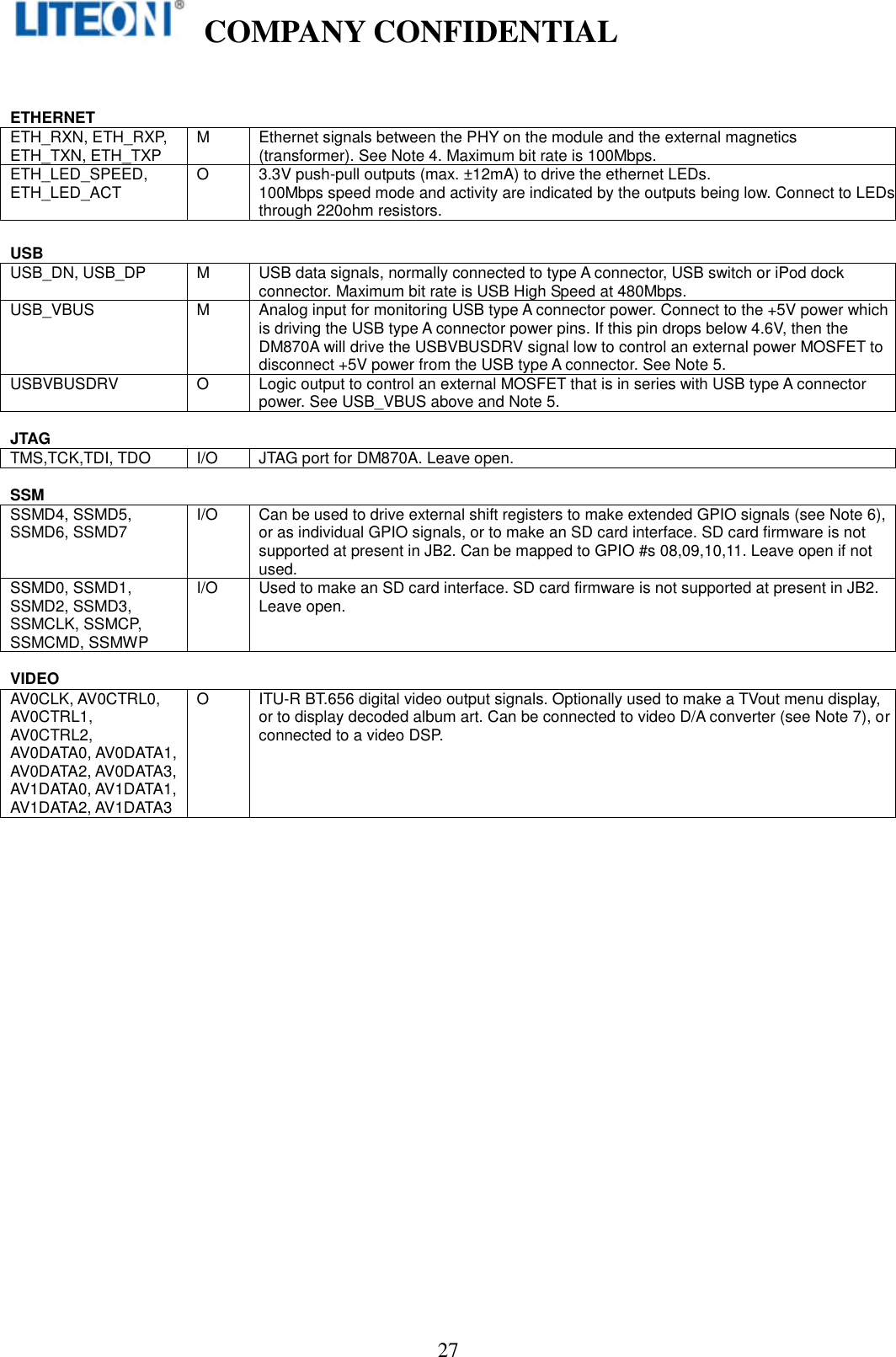
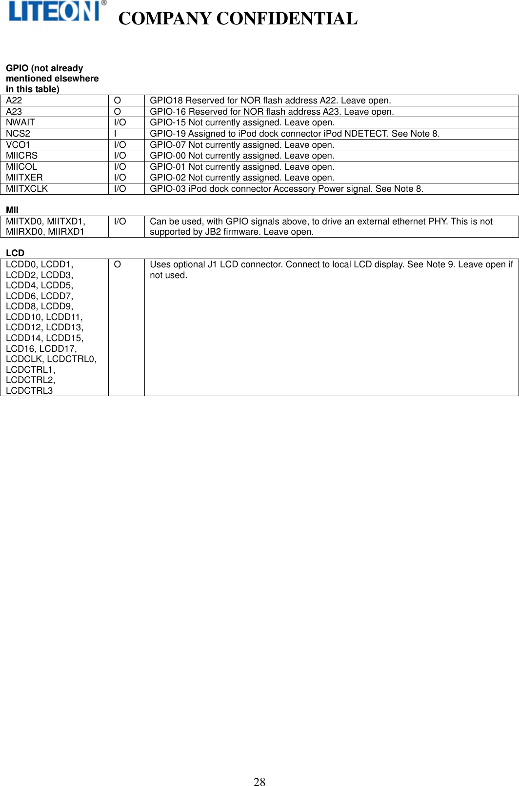
CX8703BD120 User Manual
User manual
Navigation menu
Upload a User Manual
Namespaces
Wiki Guide
HTML
PDF
Info
Views
User Manual
Discussion / Help
Navigation