LITE ON TECHNOLOGY CX8703BD120 JukeBlox Networked Media Module User Manual
LITE-ON Technology Corp. JukeBlox Networked Media Module
User manual
COMPANY CONFIDENTIAL
1
客 戶 名 稱:
Customer Name: D&M Holdings Inc.
品 名 (Part Name)
SMSC CX870-3B-D120 Module
承認書版本(Approval Sheet Rev.)
Preliminary version
客戶料號 (Customer Part No.)
光寶料號 (Liteon Part No.)
AAZ500009G0
客 戶 簽 認
Customer Approval: _________________________________________
Prepared by
Reviewed by
Approved by
Frank Gung
Total Pages
Date
Sales
40
2013/12/16
Elisa Liou
4F, 90, Chien 1 Road, Chungho, New Taipei City
235, Taiwan, R.O.C.
TEL: +886-2-2222-6181
Fax: +886-2-2222-3882
光寶科技股份有限公司
台北縣中和市建一路 90 號4F
電話: 02-2222-6181 傳真: 02-2222-3882
承 認 書
(Specification Sheet)

COMPANY CONFIDENTIAL
2
Index
Index ......................................................................................................................................................... 2
Part1. Module Spec Sheet .................................................................................................................... 5
1 Introduction .................................................................................................................................... 5
2 Block Diagram ................................................................................................................................ 5
3 Board Pictures ................................................................................................................................. 6
3.1 Top View of CX Module ........................................................................................................ 6
3.2 Bottom View of CX Module .................................................................................................. 7
3.2.1 CX Module Bottom View w/64-pin Low Density Connector ............................................. 7
3.2.2 CX Module Bottom View w/120-pin Media Connector ..................................................... 7
3.3 Production Module with Top and RF shields in place – Top View ........................................ 8
3.4 Production Module with 64-pin Connector Option – Side View ........................................... 8
3.5 Example Production Module Showing Soldered RF Shield .................................................. 9
3.6 Production Module with Bottom Shield (Part Numbers with a “B” after the configuration
letter) 10
3.6.1 Including J3 Low Density 64-pin connector – Bottom View ............................................ 10
3.6.2 Including J2 High Density 120-pin connector – Bottom View ......................................... 10
4 Ordering Guide ............................................................................................................................. 11
4.1 Part Number Syntax ............................................................................................................. 11
5 Electrical Specifications ............................................................................................................... 12
5.1 Absolute Maximum Ratings................................................................................................. 13
5.2 Operating Conditions ........................................................................................................... 13
5.3 WiFi Specification (CX870 only) ........................................................................................ 14
6 Regulatory Compliance and Quality .......................................................................................... 15
6.0.1 Antenna Considerations ............................................................................................................. 15
6.0.2 CX Power Settings Used For Modular Approval ...................................................................... 16
6.0.3 FCC IC Warning Message ......................................................................................................... 16
6.1 RoHS .................................................................................................................................... 19
6.2 Environmental Test ............................................................................................................... 19
6.3 ESD and Transient Test (Applies to LAN and USB external connections only) ................. 19
6.4 Magnetic Field Test .............................................................................................................. 20
6.5 MTBF ................................................................................................................................... 20
6.6 Mechanical Specifications .................................................................................................... 20
6.7 Module Quality .................................................................................................................... 20
7 Board Dimensions and Weight .................................................................................................... 21
7.1 Top & Bottom View of CX870 Module without Bottom Shield ......................................... 21
7.1.1 Top & Bottom View of CX Module with Bottom Shield .................................................. 21
7.2 Side View of CX870 module without Bottom Shield .......................................................... 22
7.2.1 Side View of CX Module with Bottom Shield except CX870-3JB .................................. 22
7.2.2 Side View of CX870 Module with Bottom Shield part number CX870-3JB only ........... 23
7.3 3D View of CX870 Module without Bottom Shield ............................................................ 23
7.4 Module Weight ..................................................................................................................... 23
8 Connectors and Connections ....................................................................................................... 24
8.1 WLAN UFL Antenna Connector (optional) ......................................................................... 24
8.2 Module Connectors .............................................................................................................. 24
8.2.1 Pin Descriptions ................................................................................................................ 25
8.2.2 Connector PIN Assignments ............................................................................................. 30
8.2.3 GPIO Assignments ............................................................................................................ 32
9 Application Guidelines ................................................................................................................. 32
9.1 Power Supply sequencing and Reset Timing ....................................................................... 32

COMPANY CONFIDENTIAL
3
9.1.1 Power up, Reset and Power Down Timing ....................................................................... 33
9.2 RF Considerations ................................................................................................................ 33
10 Revision Control ........................................................................................................................ 34
Part2. Antenna Spec Sheet ................................................................................................................ 42
1 RFDPA870930IMAB301 ................................................................................................................ 42
2 RFDPA870945IMAB301 ................................................................................................................ 43
COMPANY CONFIDENTIAL
4
Revision History
Date
Version
Description
12/02/2013
Rev 00
Preliminary Version for AAZ500009G0 (CX870-3B-D120)
12/16/2013
Rev 01
Add antenna spec. sheet (Part 2)
This documentation describes the marketing requirements specification of the Lite-on made
CX870 Wireless module. It is a confidential document of LITEON.
COMPANY CONFIDENTIAL
5
Part1. Module Spec Sheet
1 Introduction
The CX-series module is a single-board networked media player module, based on SMSC’s DM870A and DM875 media
processors, and enables fast product developments with Ethernet, USB and optional WiFi connectivity. The module
connects to standard legacy components in various audio, video/LCD and control formats.
2 Block Diagram
Ethernet
Transceiver
DM870A
or
DM875
256 Mbit
SDRAM
RJ-45
+
Transformer Mem.
Bus
USB
GPIO
24.000 MHz
NAND-Flash
2.4 GHz RF
transceiver
802.11
RMII
USB
Type-A
UART
3.3V
JukeBlox Networked Media Module – CX Series
1.2V
UART
GPIO
DAC
PCB
Antenna
RF Amp. ANT
switch
Ext.
Antenna
PWM DAC
1.9V
Flash
NOR-Flash
I2C
Apple Co-
processor
I2C
JTAG
JTAG
LCD
3x6bit RGB
Display
SSM
4/8bit MMC
SD-Card
RST
Reset In
Video Out
Audio I/O
A/D, D/A
S/PDIF
CCIR-656 AV
Ports
SPI
SPI Ctrl.
Host
Controller/
LCD setup
PCB
Antenna
Ext.
Antenna
Note: Choice of antenna is a build option, see Ordering Guide.
COMPANY CONFIDENTIAL
6
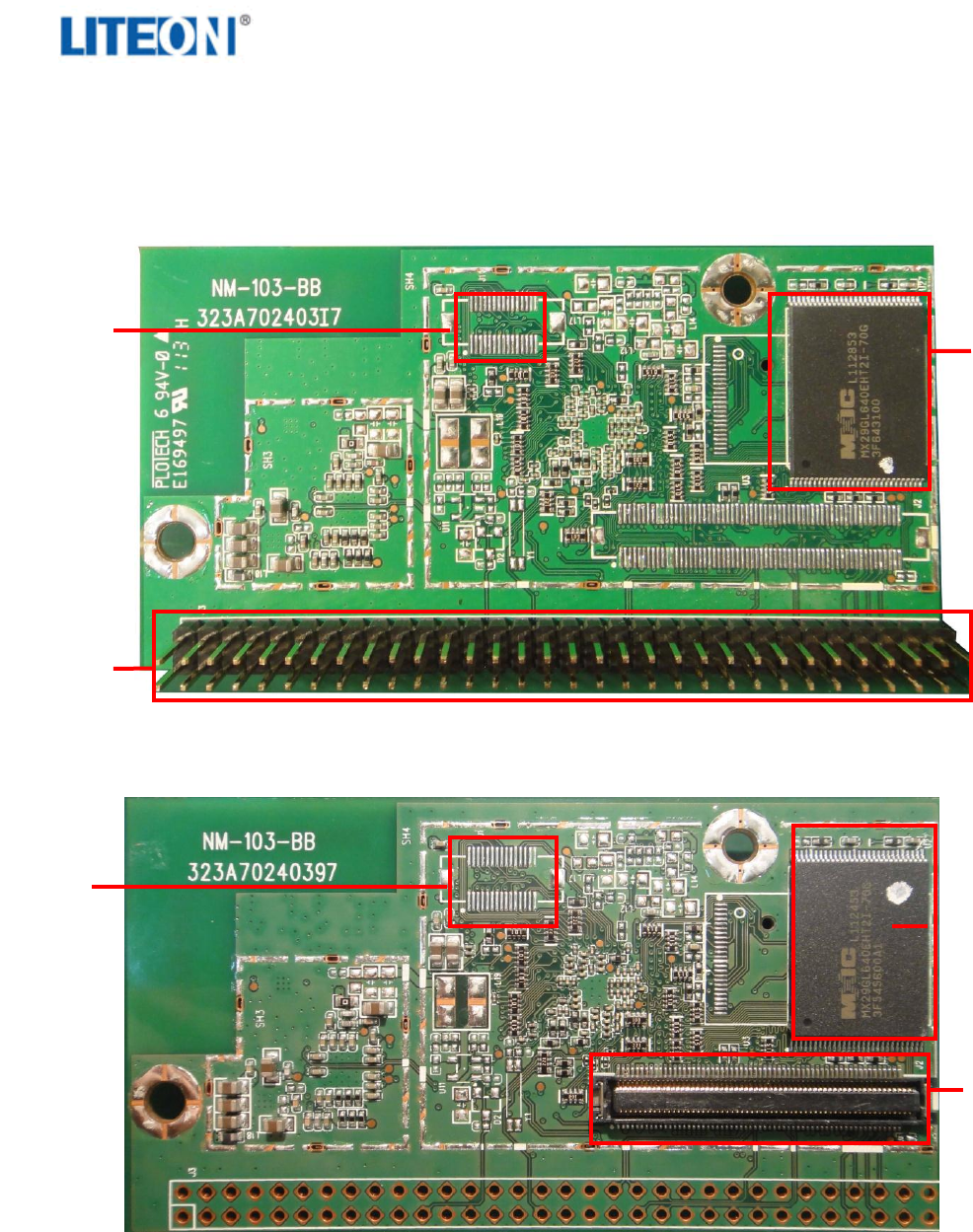
3 Board Pictures
Please note that all production modules include the RF and top shield. The below top view has the shields temporarily
removed to show the components. Also, please note that the 64-pin connector mounted on the module is the male gender.
3.1 Top View of CX Module
PCB antenna
External Antenna
Connectors
SMSC processor
Ethernet PHY
PCB antenna
SDRAM
802.11b/g
front-end
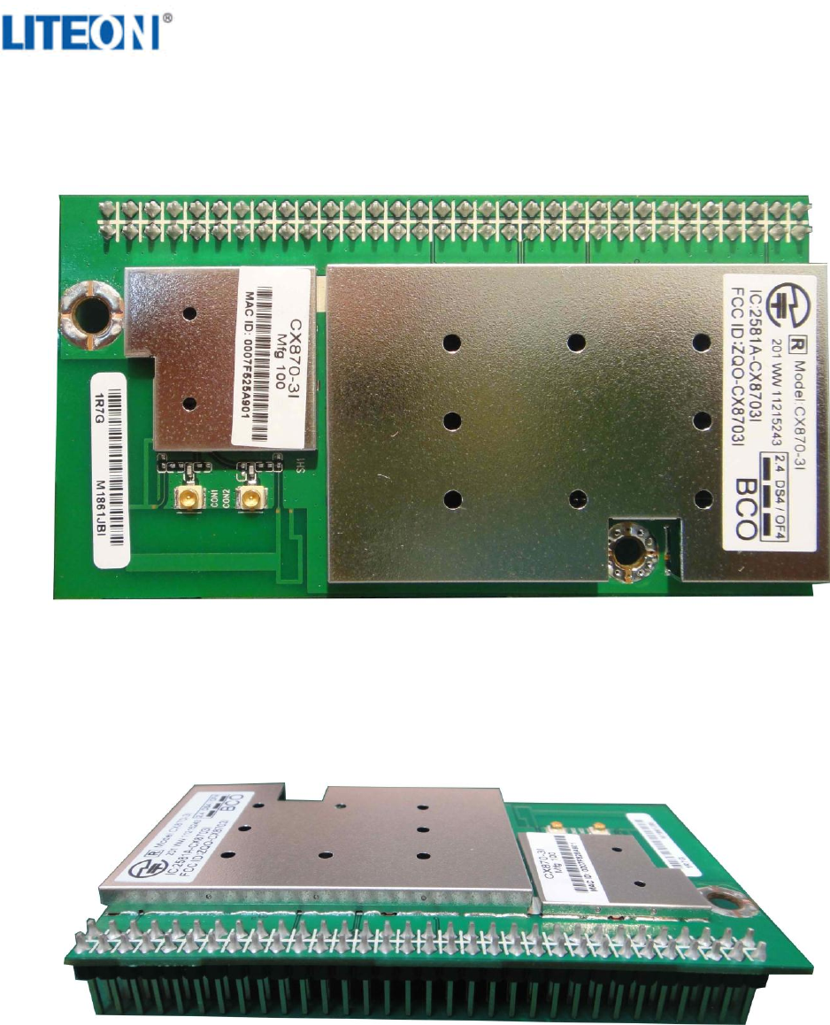
COMPANY CONFIDENTIAL
7
LCD connector
FLASH
Media
connector
FLASH
Low density
connector
3.2 Bottom View of CX Module
3.2.1 CX Module Bottom View w/64-pin Low Density Connector
3.2.2 CX Module Bottom View w/120-pin Media Connector
LCD
connector
COMPANY CONFIDENTIAL
8
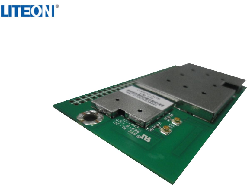
3.3 Production Module with Top and RF shields in place – Top View
3.4 Production Module with 64-pin Connector Option – Side View
COMPANY CONFIDENTIAL
9
3.5 Example Production Module Showing Soldered RF Shield
COMPANY CONFIDENTIAL
10
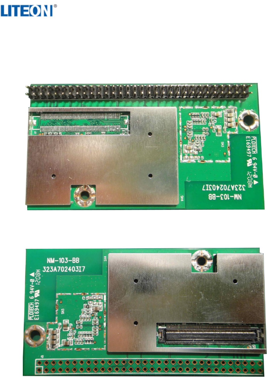
3.6 Production Module with Bottom Shield (Part Numbers with a “B”
after the configuration letter)
3.6.1 Including J3 Low Density 64-pin connector – Bottom View
3.6.2 Including J2 High Density 120-pin connector – Bottom View
COMPANY CONFIDENTIAL
11
4 Ordering Guide
One
Ant.
Two
Ant.
CX870-3B-D120 Module DM870A+T6201 Planned X X X X X X X X
CX Modules Configuration Matrix
SKU
Type
IC's
Phase
WiFi (on-
module PCB
diveristy)
Ext. Diverstiy
Antennas (UFL
Conn.s)
Eth
Top
Module
Shield
USB
Host
Low
Density
64-pin
conn.
Hi-
Density
120-pin
Conn.
Hi-
Density
LCD
Conn.
64 MB
SDRAM
32MB
SDRAM
Bottom
Module
Shield
1.9V
Status
16MB
SDRAM
8MB
SDRAM
1Gb
NAND
32MB
NOR
8MB
NOR
Note: Please note that the Apple Authentication Coprocessor will not be provided on the CX module. The Apple Authentication Coprocessor
should be provided on the product motherboard, connected to the SDA, SCL signals from the CX module.
Note: Shaded rows indicate Custom or Obsolete configuration - NOT TO BE USED FOR NEW/STANDARD MP DESIGNS.
Status code: C - Custom | S - Standard | O - Obsolete | A - Available
* Connector on board, but requires board modification to enable the connector.
+ The position of the X in the One Ant. column indicates that there is one external antenna connector provided. The position of the X in the
Two Ant. column indicates that there are two external antenna connectors provided. Do not use a module which has two external antenna
connectors with only one external antenna connected. Leaving one antenna socket open will degrade WiFi performance. SMSC
recommends always using modules with two external antennas for best performance.
% The CX870-3DS is the same as CX870-3D, except that the RF shield is soldered in place.
4.1 Part Number Syntax
COMPANY CONFIDENTIAL
12
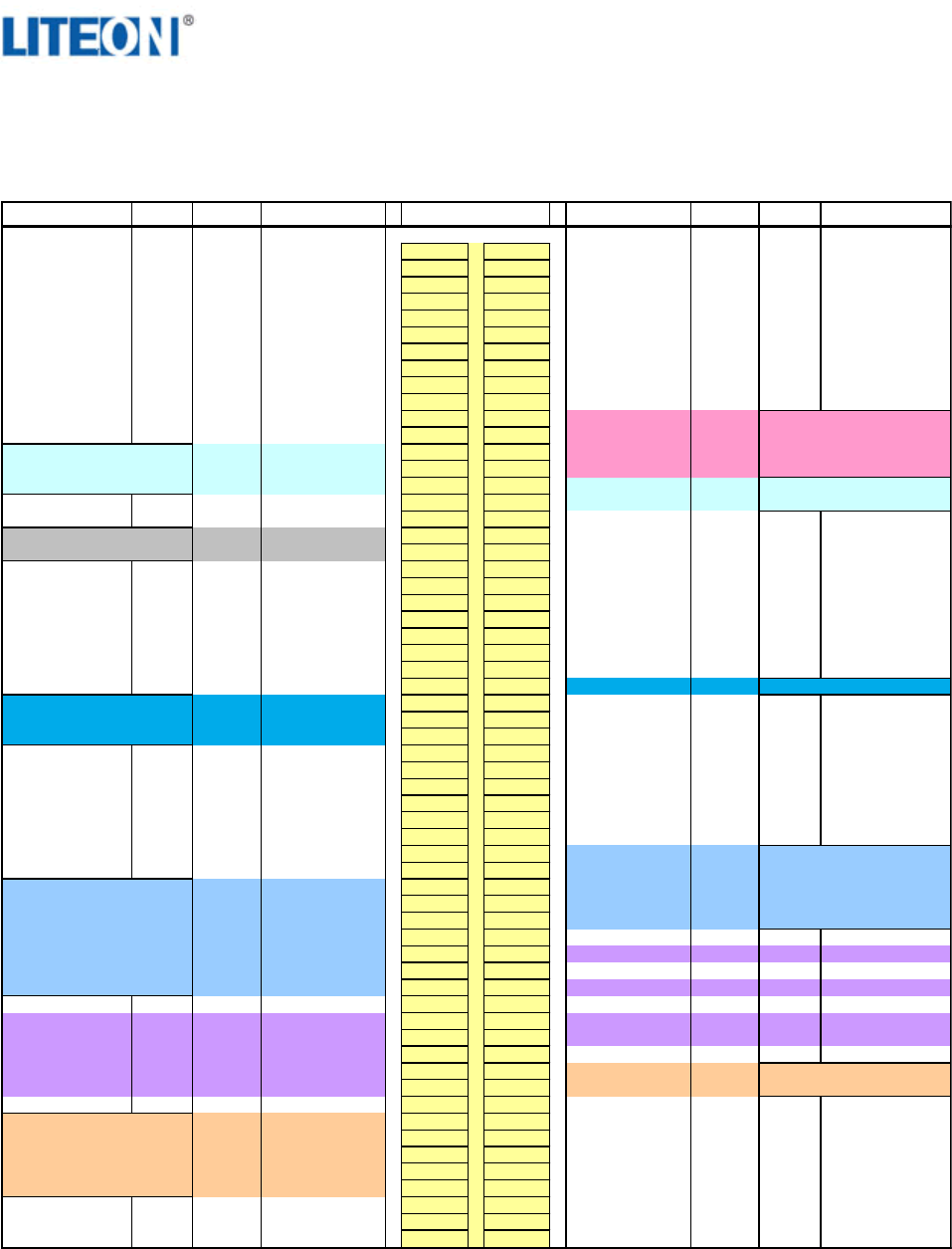
5 Electrical Specifications
Parameter
State
Model
Voltage
Symbol
min.
typ.
max.
Units
Power Supply Input Voltage
VIN
3.0
1.08
1.8
3.3
1.2
1.9
3.6
1.32
2.0
V
V
V
Logic Input high voltage
VIH
1.7
5.5
V
Logic Input low voltage
VIL
-0.3
0.7
V
Logic Input threshold voltage
VIT
1.29
1.39
1.5
V
Schmitt-trigger input low to high
threshold voltage
VIT+
1.58
1.65
1.71
V
Schmitt-trigger input high to low
threshold voltage
VIT-
0.95
1.01
1.06
V
Logic Output high voltage
VOH
2.4
V
Logic Output low voltage
VOL
0.4
V
Logic Low-level output current
(VOL=0.4V)
IOL
-9.6
-15.6
-19.3
mA
Logic High-level output current
(VOH=2.4V)
IOH
11.1
22.5
35.3
mA
Current Consumption
Reset State
CX870
3.3
I3.3
60
78
mA
1.2
I1.2
32
42
mA
1.9
I1.9
18
23
mA
Operating in
idle state
3.3
I3.3
185
241
mA
1.2
I1.2
337
438
mA
1.9
I1.9
257
334
mA
Playback over
WiFi high mips
& rate condition
3.3
I3.3
240
312
mA
1.2
I1.2
347
451
mA
1.9
I1.9
258
335
mA
Note: The maximum current values are 30% larger than the typical values. The maximum values
are intended to be used for power supply sizing calculations.
COMPANY CONFIDENTIAL
13
5.1 Absolute Maximum Ratings
Parameter
Component
Min
Max
Units
3.3V Supply Voltage
Main
-0.5
4.6
V
1.2V Supply Voltage
-0.5
1.8
V
1.9V Supply Voltage
-0.5
2.2
V
Logic Input Voltage
-0.5
6
V
Logic Output Voltage
-0.5
4.6
V
5.2 Operating Conditions
Parameter
Min
Max
Units
Operating Temperature
0
+70
°C
Operating Humidity
10
90 (non condensing)
%RH
Storage Temperature
-10
+75
°C
Storage Humidity
10
95 (non condensing)
%RH
Storage Temperature Cycle Test 24 hrs
-10
+75
°C
COMPANY CONFIDENTIAL
14
5.3 WiFi Specification (CX870 only)
Feature
Description
WLAN Standards
IEEE 802.11b
IEEE 802.11g
Frequency Band
2.412 – 2.472 GHz (2.4GHz ISM Band, 13 Channels)
Channel 1 - Channel 13
North America FCC, Japan Telec, Europe ETSI
Modulation
802.11b mode (DS-SS: IEEE 802.11b)
802.11g mode (OFDM: IEEE 802.11g)
Transmission Speed
802.11b mode
11Mbps, 5.5Mbps, 2Mbps, 1Mbps
802.11g mode
54Mbps, 48Mbps, 36Mbps, 24Mbps, 18Mbps, 12Mbps, 9Mbps,
6Mbps
Tx Power
802.11b mode: 16.5dBm, +/-1dB
802.11g mode: 15.0dBm, +/-1dB
Using nominal production settings as follows:
Channel RF11
Rate: 11B ='3' (11Mbps), 11G = '8' (54Mbps)
MIB: 11B=9, 11G=1 (Reference for Tx Power Tuning)
Room temperature
The above TX Power specifications will apply to modules shipped from Liteon
after 9 April 2012.
Power-on Ramp
< 2us
RF Carrier Suppression
< 15dBc
TX EVM
802.11b mode: <-22dB
802.11g mode: <-25dB
Rx Sensitivity
(incl. CE2 Mother board)
802.11b mode:
<=-82dBm @ 1Mbps, <=81dBm @ 2Mbps, <=-81dBm @ 5.5Mbps,
<=-78dBm @ 11Mbps
802.11g mode:
<=-82dBm @ 9Mbps, <=-81dBm @ 18Mbps, <=-75dBm @ 36Mbps,
<=-70dBm @ 54Mbps
Throughput Rate
(measured for each
module)
See factory test specification
Note: About Tx Power, different (higher/lower) RF output power settings may be used for specific
regions, antennas and/or enclosures, in which case re-certification may be required.
COMPANY CONFIDENTIAL
15
6 Regulatory Compliance and Quality
Description
Country
Compliance
Module Versions Passed
Electromagnetic Compatibility
(Prescan)
USA
Europe
FCC CFR47 Part15B
EN 55022
EN 55024
EN 61000-3-2
EN 61000-3-3
EN 61000-4-2
EN 61000-4-3
EN 61000-4-4
EN 61000-4-5
EN 61000-4-6
EN 61000-4-8
EN 61000-4-11
Radio Regulations (CX870
only)
USA
Japan
Canada
Europe
New Zealand/Australia
China
Korea
FCC Part 15C
Telec
IC RSS-210
CE
AZ/NZS:4268
SRRC
KCC
B, D, F, H, I, J
B
B, D, F, H, I, J
B
SMSC does not certify all module variants for all countries. Please see above table for those module versions for which
certain certifications have already been done.
Please contact your SMSC sales office for the latest information about which modules are certified for which countries, and
arranging for additional certification for your chosen module if needed. Any additional certifications will need to be paid for by
the customer.
Product manufacturers are responsible for the end product certification.
SMSC can help manufacturers to prepare for the WiFi Alliance tests by providing an example test plan and the required
commands to enable special test modes. Please contact your SMSC sales office about WiFi Alliance logo certification
assistance.
The CX module has received Limited Module Approval (LMA) from FCC. This is because the CX module does not have a
built-in +1.9V regulator circuit. SMSC recommends that customers follow the +1.9V supply voltage requirements given in
this data sheet, and follow the +1.9V power supply design given in “CX Module Power Supply_V1.1.pdf” document or later
version. If the power supply recommendations are followed, then customers will not need to go through formal certification of
the product for WiFi related RF behavior for FCC. It is the product manufacturers responsibility to make sure that the power
supply recommendations are followed, and that the RF behavior meets the certification requirements when the module is
installed in the final product.
Please check the SMSC/BridgeCo Customer Portal at https://portal.bridgeco.net/ for documents about WiFi certification and
recommended interfacing and power supply schematics.
6.0.1 Antenna Considerations
Here are the antennas used for certification:
Cfg Code
Ant. Type
Ant. Gain (dBi)
Ant. Model Name
CX870-3F
Printed on PCB
3.56
Liteon
N/A
CX870-3J
Dipole
2
MAG. LAYERS
EDA-8709-2G4C1-A66
CX870-3K
PIFA
2.1
MAG. LAYERS
MSA-3612-2G4C1-A1
CX870-3IB
Dipole
2
MAG. LAYERS
EDA-8709-2G4C1-A66
CX870-3B-D60
PIFA
2
2
1.7
1.7
1.7
MSA-0354-2G4C1-A3, black 200mm (max)
MSA-0345-2G4C1-A3, gray 200mm (max)
MSA-5103-2G4C1-A1, black 200mm
MSA-5403-2G4C1-A1, gray 200mm
MSA-5103-2G4C1-A3, black 300mm
COMPANY CONFIDENTIAL
16
1.7
1.7
1.7
MSA-5403-2G4C1-A3, gray 300mm
MSA-5103-2G4C1-A2, black 400mm
MSA-5403-2G4C1-A2, gray 400mm
CX870-3BB
Dipole
3.2
WINiZEN
W1E-WO-08
CX870-3HB
Dipole
2
MAG. LAYERS
EDA-8709-2G4C1-A66
CX870-3HB
PIFA
3
2.8
3010000243ID (DA-E670)
3010000218ID (DA-E750)
Notes about antenna changes:
1) Equivalent antennas from other manufacturers may be substituted, and then marketed without
a Class II permissive change
2) Equivalent antennas must be of the same type (e.g. dipole, PIFA, etc.), must be of equal or
less gain than the antennas listed and previously authorized under the same FCC ID, and must
have similar in band and out of band characteristics (consult specification sheet for cutoff
frequencies).
3) In case of new antenna types, or higher gain antennas, a Class II permissive change is
required and compliance with FCC section 15.203 must be met.
6.0.2 CX Power Settings Used For Modular Approval
6.0.3 FCC IC Warning Message
FEDERAL COMMUNICATIONS COMMISSION INTERFERENCE STATEMENT
This equipment has been tested and found to comply with the limits for a Class B digital device,
pursuant to part 15 of the FCC Rules. These limits are designed to provide reasonable protection
against harmful interference in a residential installation. This equipment generates, uses and can
radiate radio frequency energy and, if not installed and used in accordance with the instructions, may
cause harmful interference to radio communications. However, there is no guarantee that interference
will not occur in a particular installation. If this equipment does cause harmful interference to radio or
television reception, which can be determined by turning the equipment off and on, the user is
encouraged to try to correct the interference by one or more of the following measures:
-Reorient or relocate the receiving antenna.
-Increase the separation between the equipment and receiver.

COMPANY CONFIDENTIAL
17
-Connect the equipment into an outlet on a circuit different from that to which the receiver is connected.
-Consult the dealer or an experienced radio/ TV technician for help.
CAUTION:
Any changes or modifications not expressly approved by the grantee of this device could void the
user's authority to operate the equipment.
Labeling requirements
This device complies with Part 15 of the FCC Rules. Operation is
subject to the following two conditions: (1) this device may not cause
harmful interference, and (2) this device must accept any interference
received, including interference that may cause undesired operation.
RF exposure warning
This equipment must be installed and operated in accordance with provided instructions and
the antenna(s) used for this transmitter must be installed to provide a separation distance of
at least 20 cm from all persons and must not be co-located or operating in conjunction with
any other antenna or transmitter. End-users and installers must be provide with antenna
installation instructions and transmitter operating conditions for satisfying RF exposure
compliance.
Information for the OEMs and Integrators
The following statement must be included with all versions of this document supplied to an
OEM or integrator, but should not be distributed to the end user.
This device is intended for OEM integrators only.
Please See the full Grant of Equipment document for other restrictions.
This device must be operated and used with a locally approved access point.
Information To Be Supplied to the End User by the OEM or Integrator
The following regulatory and safety notices must be published in documentation supplied to
the end user of the product or system incorporating an adapter in compliance with local regulations.
Host system must be labeled with "Contains FCC ID: PPQ-CX8703BD120 “, FCC ID displayed on
label and Contains IC : 4491A-CX8703BD120.
Canada, Industry Canada (IC) Notices
This Class B digital apparatus complies with Canadian ICES-003 and RSS-210.
Operation is subject to the following two conditions: (1) this device may not cause interference, and (2)
this device must accept any interference, including interference that may cause undesired operation of the
device.
Radio Frequency (RF) Exposure Information
The radiated output power of the Wireless Device is below the Industry Canada (IC)
radio frequency exposure limits. The Wireless Device should be used in such a
manner such that the potential for human contact during normal operation is
minimized.
This device has also been evaluated and shown compliant with the IC RF Exposure
limits under mobile exposure conditions. (antennas are greater than 20cm from a
person's body).
This device has been certified for use in Canada. Status of the listing in the Industry
Canada’s REL (Radio Equipment List) can be found at the following web address:
http://www.ic.gc.ca/app/sitt/reltel/srch/nwRdSrch.do?lang=eng
Additional Canadian information on RF exposure also can be found at the following web address:
COMPANY CONFIDENTIAL
18
http://www.ic.gc.ca/eic/site/smt-gst.nsf/eng/sf08792.html
Canada, avis d'Industry Canada (IC)
Cet appareil numérique de classe B est conforme aux normes canadiennes ICES-003
et RSS-210.
Son fonctionnement est soumis aux deux conditions suivantes : (1) cet appareil ne doit pas causer
d'interférence et (2) cet appareil doit accepter toute interférence, notamment les interférences qui peuvent
affecter son fonctionnement.
Informations concernant l'exposition aux fré quences radio (RF)
La puissance de sortie émise par l’appareil de sans fil Dell est inférieure à la limite
d'exposition aux fréquences radio d'Industry Canada (IC). Utilisez l’appareil de sans
fil Dell de façon à minimiser les contacts humains lors du fonctionnement normal.
Ce périphérique a également été évalué et démontré conforme aux limites
d'exposition aux RF d'IC dans des conditions d'exposition à des appareils mobiles
(les antennes se situent à moins de 20 cm du corps d'une personne).
Ce périphérique est homologué pour l'utilisation au Canada. Pour consulter l'entrée
correspondant à l’appareil dans la liste d'équipement radio (REL - Radio Equipment
List) d'Industry Canada rendez-vous sur:
http://www.ic.gc.ca/app/sitt/reltel/srch/nwRdSrch.do?lang=eng
Pour des informations supplémentaires concernant l'exposition aux RF au Canada rendez-vous sur :
http://www.ic.gc.ca/eic/site/smt-gst.nsf/eng/sf08792.html
Information To Be Supplied to the End User by the OEM or Integrator
The following regulatory and safety notices must be published in documentation supplied to the end user of the product or system
incorporating an adapter in compliance with local regulations. Host system must be labeled with "Contains IC: 740B-VX77A “, IC ID
displayed on label.
This radio transmitter FCCID: PPQ-CX8703BD120 has been approved by FCC to operate with the antenna types listed
below with the maximum permissible gain and required antenna impedance for each antenna type indicated. Antenna types
not included in this list, having a gain greater than the maximum gain indicated for that type, are strictly prohibited for use
with this device.
Antenna List
No.
Manufacturer
Model No.
Peak Gain
1
Walsin
RFDPA870920IMAB301 (200mm)(Main)(Aux)
2.14 dBi
2
Walsin
RFDPA870930IMAB301(300mm) (Main)(Aux)
1.2 dBi
3
Walsin
RFDPA870945IMAB301(450mm) (Main)(Aux)
1.16 dBi
4
Walsin
RFDPA870900SBAB801 +
RFCBA100645SA6B301(450mm) (Main)(Aux)
0.2 dBi
5
Walsin
RFDPA870900SBAB801 +
RFCBA100630SA6B301(300mm) (Main)(Aux)
0.3 dBi
6
Walsin
RFDPA870900SBAB801 +
RFCBA100620SA6B301(200mm) (Main)(Aux)
0.4 dBi
Note: The antenna connector is Reverse SMA type.
This radio transmitter IC: 4491A-CX8703BD120 has been approved by Industry Canada to operate with
the antenna types listed below with the maximum permissible gain and required antenna impedance for each antenna type
indicated. Antenna types not included in this list, having a gain greater than the maximum gain indicated for that type, are
strictly prohibited for use with this device.
Cet émetteur radio IC: 4491A-CX8703BD120 a été approuvé par Industrie Canada pour fonctionner avec les types
d'antennes énumérés ci‐dessous avec le gain maximal admissible et impédance d'antenne requise pour chaque
type d'antenne indiqué. Types d'antennes n'est pas inclus dans cette liste, ayant un gain supérieur au gain
maximal indiqué pour ce type, sont strictement interdits pour une utilisation avec cet appareil.
COMPANY CONFIDENTIAL
19
Antenna List
No.
Manufacturer
Model No.
Peak Gain
1
Walsin
RFDPA870920IMAB301 (200mm)(Main)(Aux)
2.14 dBi
2
Walsin
RFDPA870930IMAB301(300mm) (Main)(Aux)
1.2 dBi
3
Walsin
RFDPA870945IMAB301(450mm) (Main)(Aux)
1.16 dBi
4
Walsin
RFDPA870900SBAB801 +
RFCBA100645SA6B301(450mm) (Main)(Aux)
0.2 dBi
5
Walsin
RFDPA870900SBAB801 +
RFCBA100630SA6B301(300mm) (Main)(Aux)
0.3 dBi
6
Walsin
RFDPA870900SBAB801 +
RFCBA100620SA6B301(200mm) (Main)(Aux)
0.4 dBi
Note: The antenna connector is Reverse SMA type.
6.1 RoHS
Uses only RoHS compliant components
6.2 Environmental Test
Withstands 4 hours at 70°C, 90% RH
6.3 ESD and Transient Test (Applies to LAN and USB external
connections only)
ESD: +/- 2kV operation, +/- 4kV no destruction (part of CE test)
Fast electrical transients: +/- 500V operation, +/- 1000V no destruction (part of CE test)

COMPANY CONFIDENTIAL
20
6.4 Magnetic Field Test
Passes EN55022 and EN55024 (part of CE test)
6.5 MTBF
>10000 hours
6.6 Mechanical Specifications
Passes drop test according to I.E.C. 68-2-32, height 100 cm, 1 corner, 6 faces.
Passes vibration test with sine, vertical, 60 minutes, 600 to 18000 cpm, 1G
6.7 Module Quality
Defect Rate: < 1%
AQL CR=0, MA=0.4, MI=0.4
COMPANY CONFIDENTIAL
21
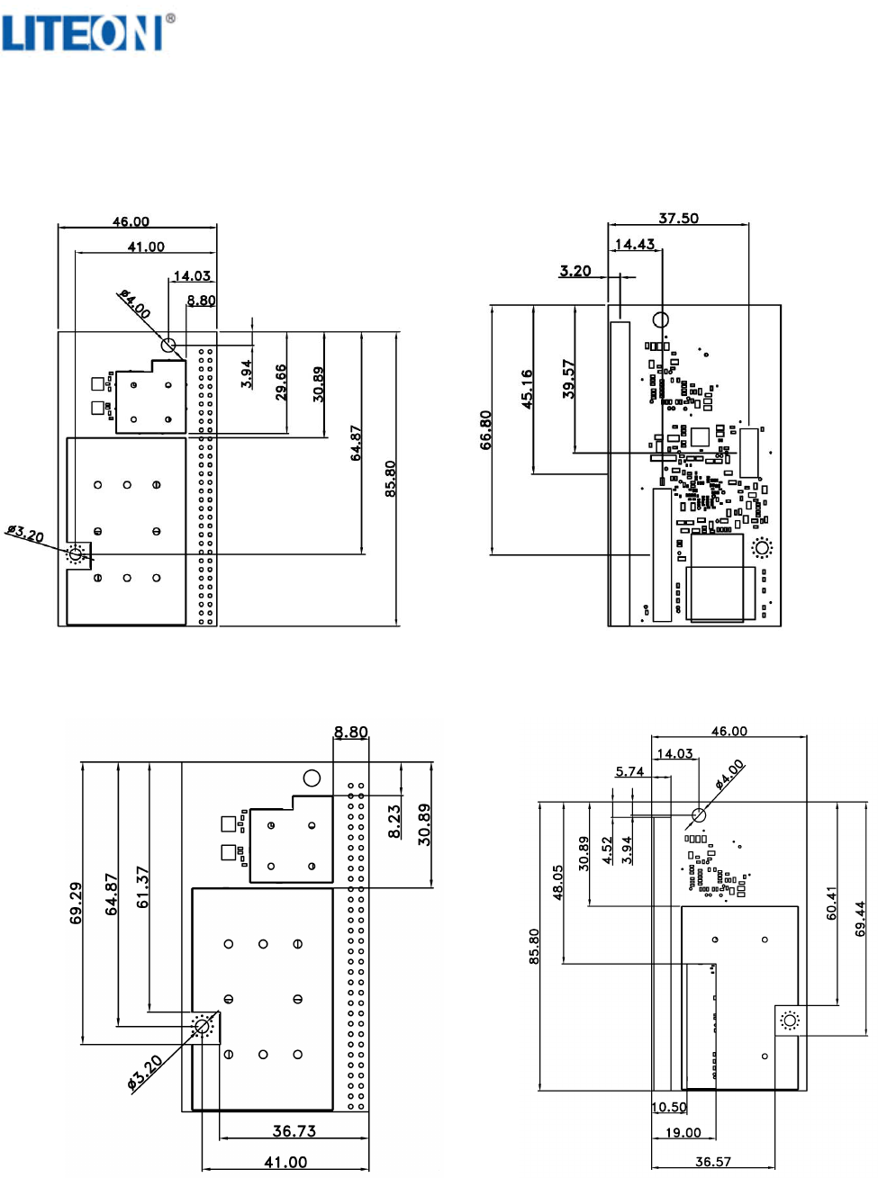
7 Board Dimensions and Weight
7.1 Top & Bottom View of CX870 Module without Bottom Shield
7.1.1 Top & Bottom View of CX Module with Bottom Shield
COMPANY CONFIDENTIAL
22
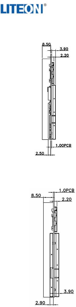
7.2 Side View of CX870 module without Bottom Shield
7.2.1 Side View of CX Module with Bottom Shield except CX870-3JB
Note:
1. All dimensions are measured in millimetres (mm).
2. PCB’s thickness: 1.00 +/- 0.10mm
3. Tolerance: +/-0.10mm
4. Outline Tolerance: +/-0.10mm
5. NPTH Hole: +/-0.05mm
6. PTH Hole: +/-0.075mm
7. Connector positions, board dimensions, mounting
hole positions and sizes are the same for all module
variants.
8. Connector position tolerance: +/- 0.38mm
9. The 64-pin connector mounted on the module along
one edge is the male gender.
10. Not all module variants have all connectors. Please
see the Ordering Guide table for details of connector
options.
COMPANY CONFIDENTIAL
23
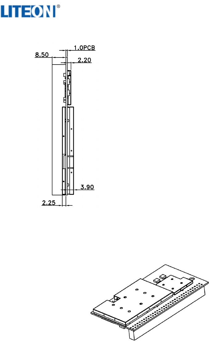
7.2.2 Side View of CX870 Module with Bottom Shield part number CX870-3JB only
7.3 3D View of CX870 Module without Bottom Shield
Note: A 3D file of the CX module in .stp format is available from
the SMSC Customer Portal.
7.4 Module Weight
CX870: 20g
Note: Module weight applies to all versions of the module.
COMPANY CONFIDENTIAL
24
8 Connectors and Connections
8.1 WLAN UFL Antenna Connector (optional)
The module includes two PCB strip antennas operated in diversity mode. Alternatively, one or two coaxial antenna
connectors are provided for connecting external (to the module) antennas. The choice between using the strip antenna or
using the coaxial sockets is a build option, determined by the position of surface mount capacitors on the module PCB. If the
PCB antennas are chosen, then diversity mode is always used. If external (to the module) antenna sockets are used, then
two external antennas should be used to provide 2X diversity operation.
If external antenna is used, please choose the proper part number indicating two external antenna sockets. Do not use a
module which has two external antenna sockets with only one external antenna connected; this will result in reduced WiFi
performance.
Please see ordering guide for build option details.
The surface-mount antenna socket used in the CX module is:
UF.L type Ultra Small Surface Mount Coaxial Connector
8.2 Module Connectors
The CX860/870 module uses 3 board-to-board connectors as interfaces to the product main board. The part numbers for the
connectors needed on the product main board, which mate with the connectors on the CX module, are shown in the table
below.
Connector
Number
Connector
Purpose
Connector
Type
Number
of Pins
Pin
Configuration
Mating Connector Part Numbers
J1
LCD
B2B
Connector
30
2 x 15 x 0.5mm
14-5046-030-145-829+ (Kyocera)
J2
Media
120
2 x 60 x 0.5mm
14-5046-120-145-829+ (Kyocera)
J3
Low Density
64
2 x 32 x 2.54mm
CSHA201-3202A001A1AB
COMPANY CONFIDENTIAL
25
The pinout and signal names are shown on the next page. The following table provides an overview for the most important
control and interface signals.
8.2.1 Pin Descriptions
Signal(s)
Type
Description
POWER
VIN(+3.3V)
P
Power supply input ; +3.3V.
VIN (+1.2V)
P
Power supply input ; +1.2V.
VIN (+1.9V)
P
Power Supply input; +1.9V for powering RF section. Make sure this is a clean supply.
3V3RTC
P
The RTC function is no longer supported. This pin should be left open.
GND
P
Ground (GND) connection for power supply 0V, signal returns and shielding.
SPI
SPI_DOUT
O
SPI data from DM870A to host controller.
SPI_DIN
I
SPI data from host controller to DM870A.
SPI_CLK
I
SPI clock from host controller to DM870A. Maximum recommended frequency is 2MHz,
typical frequency is 1MHz. See Note 2 below.
SPI_NCS0
I
SPI chip select from host controller to DM870A.
PDOUT1
O
This signal is used as SPI_REQ, SPI request signal, from DM870A to host controller for
eDMP applications. Logic 1 indicates that there is an SPI message waiting to be read, the
host controller should start the SPI clock and read any changed registers. Logic 0
indicates that all changed register messages have been read and the message buffer is
empty. Also GPIO-06.
SPI_NCS1
I
Not used. Leave open.
UART
RXD1
I
UART1 input to the DM870A, used for shell access. SMSC recommends providing a
connection to an external RS-232 transceiver and DB9 connector to connect to a PC COM
port. Such a connection can be used for product development debugging, and for module
programming control on the product manufacturing line and for module control during
certification procedures.
TXD1
O
UART1 output from the DM870A, used for shell access. SMSC recommends providing a
connection to an external RS-232 transceiver and DB9 connector to connect to a PC COM
port. Such a connection can be used for product development debugging, and for module
programming control on the product manufacturing line and for module control during
certification procedures.
RXD0
I
UART0 input. Optionally used for controlling an iPod via UART.
TXD0
O
UART0 output. Optionally used for controlling an iPod via UART.
COMPANY CONFIDENTIAL
26
AUDIO
AV2DATA0
O
I2S or left justified audio data output. Typically connected to external D/A converter input
or to external DSP for further audio processing. Used for main left and right channel audio
output data. See Note 3.
AV2CTRL0
O
LRCK, audio data word clock at the audio sample rate (Fs). Maximum currently supported
frequency is 192kHz.
AV2CTRL1
O
MCLK, audio master clock at 256Fs. This can be used to clock an external D/A converter
or DSP.
AV2CLK
O
SCLK, audio data bit clock at 64Fs. Allows for up to 32 audio data bits per sample word.
AV4DATA1
O
SPDIF format output. Can support samples rates up to 192kHz, so the maximum
instantaneous frequency on this pin is 24.576MHz.
AV4DATA0
I
SPDIF input. Not used at present. Leave open.
AV2DATA1
O
I2S or left justified audio data output. Not used at present. Leave open.
AOUTLP/AOUTLN,
AOUTRP/AOUTRN
O
Differential stereo output from PWM-DAC, right and left channels. These signals require
analog low pass filtering. SMSC is not recommending using the PWM-DAC outputs
because of the potential for high out-of-band noise and uncharacterized audio quality.
SMSC recommends using an external D/A converter connected to AV2DATA0.
AV2DATA2
I
I2S or left justified audio data input. Can be driven from an optional external A/D converter
used to interface to iPod analog output or other analog audio sources. If not used, leave
open.
AV2DATA3
I
I2S or left justified audio data input. Not used at present. Leave open.
CONTROL
NCS3
I
This signal is configured as GPIO-17 and is currently not used. DM870A-internal pull-up.
Leave this pin open.
PDOUT0
I
Factory Reset. GPIO-04. Return the CnE to factory settings. High-active input,
DM870A-internal pull-down. Pull to GND with a 10kohm resistor, unless return to factory
settings from a hardware control is needed. Normally, return to factory settings is controlled
from the host controller via SPI register. This pin is only monitored during the boot up
process.
VCO0
I
Infrared sensor input. GPIO-05. This is a Schmitt-Trigger input and can handle inputs with
slow slopes. Used for aDMP firmware builds for infrared remote control sensor output
connection to DM870A. For applications with a host controller, pull this pin to +3.3V via a
10kohm resistor.
AV3CLK
O
ETH_NRESET Low-active reset for the on-board ethernet PHY. This output is driven by the
DM870A. GPIO-12. Leave this pin open.
AV3CTRL0, AV3CTRL1
I/O
I2C_SCL, I2C_SDA bus created by GPIO-13 and GPIO-14.
No internal pull-ups; Use 4.7kohm pull up resistor on each pin to +3.3V. Maximum
frequency is 400kHz.
NRESET_MOD
I
Low-active input to reset the module. This signal must be driven by an external reset
generator, or by a GPIO output from a host controller. See the application section of this
data sheet for the timing requirements for NRESET_MOD. Includes internal 10K pull-up
resistor to +3.3V.
NPD_RF
I
Active low input to shut down the power for the 802.11 RF section. Internal 10kohm
pull-up resistor to +3.3V. Leave open if powering down the RF section is not required.
COMPANY CONFIDENTIAL
27
ETHERNET
ETH_RXN, ETH_RXP,
ETH_TXN, ETH_TXP
M
Ethernet signals between the PHY on the module and the external magnetics
(transformer). See Note 4. Maximum bit rate is 100Mbps.
ETH_LED_SPEED,
ETH_LED_ACT
O
3.3V push-pull outputs (max. ±12mA) to drive the ethernet LEDs.
100Mbps speed mode and activity are indicated by the outputs being low. Connect to LEDs
through 220ohm resistors.
USB
USB_DN, USB_DP
M
USB data signals, normally connected to type A connector, USB switch or iPod dock
connector. Maximum bit rate is USB High Speed at 480Mbps.
USB_VBUS
M
Analog input for monitoring USB type A connector power. Connect to the +5V power which
is driving the USB type A connector power pins. If this pin drops below 4.6V, then the
DM870A will drive the USBVBUSDRV signal low to control an external power MOSFET to
disconnect +5V power from the USB type A connector. See Note 5.
USBVBUSDRV
O
Logic output to control an external MOSFET that is in series with USB type A connector
power. See USB_VBUS above and Note 5.
JTAG
TMS,TCK,TDI, TDO
I/O
JTAG port for DM870A. Leave open.
SSM
SSMD4, SSMD5,
SSMD6, SSMD7
I/O
Can be used to drive external shift registers to make extended GPIO signals (see Note 6),
or as individual GPIO signals, or to make an SD card interface. SD card firmware is not
supported at present in JB2. Can be mapped to GPIO #s 08,09,10,11. Leave open if not
used.
SSMD0, SSMD1,
SSMD2, SSMD3,
SSMCLK, SSMCP,
SSMCMD, SSMWP
I/O
Used to make an SD card interface. SD card firmware is not supported at present in JB2.
Leave open.
VIDEO
AV0CLK, AV0CTRL0,
AV0CTRL1,
AV0CTRL2,
AV0DATA0, AV0DATA1,
AV0DATA2, AV0DATA3,
AV1DATA0, AV1DATA1,
AV1DATA2, AV1DATA3
O
ITU-R BT.656 digital video output signals. Optionally used to make a TVout menu display,
or to display decoded album art. Can be connected to video D/A converter (see Note 7), or
connected to a video DSP.
COMPANY CONFIDENTIAL
28
GPIO (not already
mentioned elsewhere
in this table)
A22
O
GPIO18 Reserved for NOR flash address A22. Leave open.
A23
O
GPIO-16 Reserved for NOR flash address A23. Leave open.
NWAIT
I/O
GPIO-15 Not currently assigned. Leave open.
NCS2
I
GPIO-19 Assigned to iPod dock connector iPod NDETECT. See Note 8.
VCO1
I/O
GPIO-07 Not currently assigned. Leave open.
MIICRS
I/O
GPIO-00 Not currently assigned. Leave open.
MIICOL
I/O
GPIO-01 Not currently assigned. Leave open.
MIITXER
I/O
GPIO-02 Not currently assigned. Leave open.
MIITXCLK
I/O
GPIO-03 iPod dock connector Accessory Power signal. See Note 8.
MII
MIITXD0, MIITXD1,
MIIRXD0, MIIRXD1
I/O
Can be used, with GPIO signals above, to drive an external ethernet PHY. This is not
supported by JB2 firmware. Leave open.
LCD
LCDD0, LCDD1,
LCDD2, LCDD3,
LCDD4, LCDD5,
LCDD6, LCDD7,
LCDD8, LCDD9,
LCDD10, LCDD11,
LCDD12, LCDD13,
LCDD14, LCDD15,
LCD16, LCDD17,
LCDCLK, LCDCTRL0,
LCDCTRL1,
LCDCTRL2,
LCDCTRL3
O
Uses optional J1 LCD connector. Connect to local LCD display. See Note 9. Leave open if
not used.

COMPANY CONFIDENTIAL
29
Notes:
1. Signal type codes:
I – 3.3V level Digital Logic Input into the DM870A
O – 3.3V level Digital Logic Output from the DM870A
IO – 3.3V level Digital Logic Input and Output (bi-directional) signal
M – Miscellaneous, see text for description
P – Power Supply
2. For SPI timing diagram for eDMP applications, please see:
BridgeCo_JB2x - DeviceControlProtocol_Registers_v_2_1.pdf, or later version.
For detailed setup and hold timing details, see DM870A IC data sheet:
DM870A DS rev. 1.3_12-15-11.pdf, or later version.
3. For audio port timing diagrams, and for detailed setup and hold timing, please see DM870A IC data sheet:
DM870A DS rev. 1.3_12-15-11.pdf, or later version.
4. For example ethernet external schematic, see:
CX Module Ethernet (RJ45 + Ext.Magnetics)_V1.2.pdf, or later version.
This schematic is typically compressed into a zip file, for example:
CX Module_Interface Schematics_one_page_V1.2_Jun_11.rar
5. For example USB schematics, see:
CX Module USB_V1.2.pdf, or later version.
This schematic is typically compressed into a zip file, for example:
CX Module_Interface Schematics_one_page_V1.2_Jun_11.rar
6. For example use of extended GPIO shift registers, see CE2 schematic:
A EVMCE2-4_schematic.pdf, or later version.
7. For example connection to a video D/A converter, see CE2 schematic:
A EVMCE2-4_schematic.pdf, or later version.
8. iPod dock connector pin and GPIO assignments are under discussion. Please contact SMSC for
recommendations for iPod dock connections to CX870 module.
9. For example connection to an LCD display, see CE2 schematic:
A EVMCE2-4_schematic.pdf, or later version.
10. All the above signals are brought out to J2 pins. Not all the above signals are brought out to J3, the 64-pin
low density connector. The J3 pin assignments table shows which signals are brought out to the J3 pins.
11. SMSC has a set of example motherboard schematics that shows example external circuitry that is typically
connected to the module. Please check the SMSC/BridgeCo customer portal at https://portal.bridgeco.net/
for a copy of these example schematics. These schematics are typically compressed into a zip file, for
example:
CX Module_Interface Schematics_one_page_V1.2_Jun_11.rar
12. Please check the SMSC/BridgeCo Customer Portal Download area for the latest version of the SMSC
documents. Go to https://portal.bridgeco.net/. If you do not have an account, please contact SMSC.
COMPANY CONFIDENTIAL
30
8.2.2 Connector PIN Assignments
J2 – Media Connector
Function GPIO IC PIN Signal Signal IC PIN GPIO Function
GND 1 2 GND
VIN (+3.3V) 3 4 VIN (+3.3V)
VIN (+3.3V) 5 6 VIN (+3.3V)
GND 7 8 GND
VIN (+1.2V) 9 10 VIN (+1.2V)
VIN (+1.2V) 11 12 VIN (+1.2V)
GND 13 14 GND
VIN (+1.9V) 15 16 VIN (+1.9V)
GND 17 18 GND
3V3RTC 19 20 GND
GND 21 22 TMS B15
GND 23 24 TCK C14
D15 SPI_DOUT 25 26 TDI A16
D14 SPI_DIN 27 28 TDO A15
B16 SPI_CLK 29 30 SPI_NCS0 C15
C13 TXD0 31 32 SPI_NCS1 B17
B14 RXD0 33 34 NRESET_MOD Module reset input
A14 RXD1 35 36 SSMD6 C12 GPIO-10 SPI_E_CLK
B13 TXD1 37 38 SSMD4 A12 GPIO-08 SPI_E_SDO
GND 39 40 SSMD2 C11
SPI_E_NCS GPIO-11 D12 SSMD7 41 42 SSMD1 B11
SPI_E_SDI GPIO-09 B12 SSMD5 43 44 SSMCMD A13
D11 SSMD3 45 46 SSMWP D9
A11 SSMD0 47 48
NCS3 H18 GPIO-17 BIST activate
C10 SSMCLK 49 50 NCS2 J17 GPIO-19 iPod NDETECT
D10 SSMCP 51 52 GND
GND 53 54 USB_VBUS D2
A1 USB_DN 55 56 GND
B1 USB_DP 57 58 AOUTRN L3
E3 USBVBUSDRV 59 60 AOUTRP L4
GND 61 62 GND
K4 AOUTLP 63 64 PDOUT1 J1 GPIO-06 SPI_REQ
L2 AOUTLN 65 66 VCO1 J2 GPIO-07
GND 67 68
PDOUT0 K1 GPIO-04 Factory reset
GPIO-16 H17 A23 69 70
VCO0 K2 GPIO-05 IR input
GPIO-18 H16 A22 71 72
AV3CLK R4 GPIO-12 ETH NRESET
I2C SDA GPIO-14 T3 AV3CTRL1 73 74 AV0CTRL0 M1
I2C SCL GPIO-13 U2 AV3CTRL0 75 76 AV1DATA3 N4
M3 AV0CTRL2 77 78 AV1DATA2 P1
M2 AV0CTRL1 79 80 AV1DATA1 P2
L1 AV0CLK 81 82 AV1DATA0 P3
M4 AV0DATA3 83 84 GND
N1 AV0DATA2 85 86 AV2CTRL1 T1 MCLK
N2 AV0DATA1 87 88 GND
N3 AV0DATA0 89 90 AV2CLK R1 SCLK
GND 91 92 GND
LRCK T1 AV2CTRL0 93 94 AV4DATA1 U3 SPDIF output
A/D data 1 P4 AV2DATA3 95 96 AV4DATA0 V2 SPDIF input
A/D data 0 R3 AV2DATA2 97 98 GND
D/A data 1 T2 AV2DATA1 99 100 ETH_LED_ACT
D/A data 0 U1 AV2DATA0 101 102 ETH_LED_SPEED
GND 103 104 MIICRS R14 GPIO-00
ETH_RXN 105 106 MIICOL T13 GPIO-01
ETH_RXP 107 108 MIITXER T11 GPIO-02
109 110 MIITXCLK R12 GPIO-03 iPod Access Power
ETH_TXN 111 112 MIITXD0 U10
ETH_TXP 113 114 MIITXD1 V10
GND 115 116 MIIRXD0 U12
GPIO-15 K18 NWAIT 117 118 MIIRXD1 V12
NPD_RF 119 120 GND
USB
Video Output
Ethernet
USB
Video Output
Ethernet
PIN Number
SPI
Debug UART
JTAG
SPI
Note: The IC PIN column indicates the pin number on the DM860A or DM870A integrated circuit. This
allows for easy cross-reference to the DM860A or DM870A data sheet information.
COMPANY CONFIDENTIAL
31
J1 – LCD Connector
Function GPIO IC PIN Signal Signal IC PIN GPIO Function
GND
1 2 GND
V8 LCDD0
3 4 LCDD1 U8
T8 LCDD2
5 6 LCDD3 R8
V7 LCDD4
7 8 LCDD5 U7
T7 LCDD6
910 LCDD7 R7
V6 LCDD8
11 12 LCDD9 U6
T6 LCDD10
13 14 LCDD11 R6
V5 LCDD12
15 16 LCDD13 U5
T5 LCDD14
17 18 LCDD15 V4
U4 LCDD16
19 20 LCDD17 V3
GND
21 22 GND
T10 LCDCLK
23 24 LCDCTRL0 R9
T9 LCDCTRL1
25 26 LCDCTRL2 U9
V9 LCDCTRL3
27 28 GND
GND 29 30 GND
PIN Number
LCD Interface
LCD Interface
LCD Interface
LCD Interface
Note: The IC PIN column indicates the pin number on the DM860A or DM870A integrated circuit. This
allows for easy cross-reference to the DM860A or DM870A data sheet information.
J3 – Low Density Connector
Function GPIO IC PIN Signal Signal IC PIN GPIO Function
GND
1 2 GND
VIN (+3.3)
3 4 RXD0 B14
VIN (+3.3)
5 6 TXD0 C13
GND
7 8 GND
VIN (+1.9)
910 VIN (+1.2)
VIN (+1.9)
11 12 VIN (+1.2)
GND
13 14 GND
Free GPIO-15 K18 NWAIT
15 16 RXD1 A14
iPod NDETECT GPIO-19 J17 NCS2
17 18 TXD1 B13
D13 NRESET
19 20 GND
3V3RTC
21 22 AV2CTRL1 R2 MCLK
GND
23 24 AV2CTRL0 T1 LRCK
D14 SPI_DIN
25 26 AV2CLK R1 SCLK
D15 SPI_DOUT
27 28 AV2DATA2 R3 A/D data 0
B16 SPI_CLK
29 30 AV2DATA0 U1 D/A data 0
C15 SPI_NCS0
31 32 AV4DATA1 T2 SPDIF output
Free GPIO-17 H18 NCS3
33 34 AV4DATA0 V2 SPDIF input
GND
35 36 GND
E-GPIO_NCS/TBA GPIO-11 D12 SSMD7
37 38 USB_DN A1
I2C SDA GPIO-14 T3 AV3CTRL1
39 40 USB_DP B1
I2C SCL GPIO-13 U2 AV3CTRL0
41 42 USBVBUSDRV E3
GND
43 44 USB_VBUS D2
SPI_REQ GPIO-06 J1 PDOUT1
45 46 GND
Factory Reset GPIO-04 K1 PDOUT0
47 48 SSMD5 B12 GPIO-09 E-GPIO_SDI/TBA
IR input GPIO-05 K2 VCO0
49 50 SSMD4 A12 GPIO-08 E-GPIO_SDO/TBA
GND
51 52 GND
ETH_LED_SPEED
53 54 ETH_LED_ACT
iPod Access Power GPIO-03 R12 MIITXCLK
55 56 SSMD6 C12 GPIO-10 E-GPIO_CLK/TBA
ETH_RXN
57 58 ETH_RXP
ETH_TXN
59 60 ETH_TXP
Free GPIO-00 R14 MIICRS
61 62 MIICOL T13 GPIO-01 Free
GND 63 64 GND
PIN Number
Debug UART
USB
SPI
Ethernet
Ethernet
Ethernet
Ethernet
Note: The IC PIN column indicates the pin number on the DM860A or DM870A integrated circuit. This
allows for easy cross-reference to the DM860A or DM870A data sheet information.
COMPANY CONFIDENTIAL
32
8.2.3 GPIO Assignments
GPIO Assignments for J3 64-pin Low Density Connector
GPIO
PIN Name
PIN Number
Function
00
MIICRS
61
Free
01
MIICOL
62
Free
03
MIITXCLK
55
iPOD Access Power
04
PDOUT0
47
Factory Reset
05
VCO0
49
IR Input
06
PDOUT1
45
Host NIREQ
08
SSMD4
50
E_GPIO_SDO/TBA
09
SSMD5
48
E_GPIO_SDI/TBA
10
SSMD6
56
E_GPIO_CLK/TBA
11
SSMD7
37
E_GPIO_NCS/TBA
13
AV3CTRL0
41
I2C_SCL
14
AV3CTRL1
39
I2C_SDA
15
NWAIT
15
Free
17
NCS3
33
Free
19
NCS2
17
IPOD NDETECT
Note: Not all 20 GPIO signals are brought out to J3 64-pin low density connector. For the CX870-3K, GPIOs 00,
01 and 03 are not brought out to J3 64-pin low density connector. J3 pin numbers 61, 62 and 55 are not
connected to any signal in the CX870-3K module.
9 Application Guidelines
9.1 Power Supply sequencing and Reset Timing
There are strict power sequencing and reset timing requirements.
Power up the I/O voltage (3.3V) first and hold NRESET_MOD low.
The core voltage (1.2V) must never be higher than (I/O voltage +0.5 V).
The core voltage (1.2V) must be within the specified core voltage limits less than 300ms after the I/O voltage (3.3V)
reaches the specified I/O voltage limits.
Throughout the power down process, the 3.3V supply must maintain a higher voltage than the 1.2V supply, until both
have reached ground potential.
To assure a proper IC reset, the power supplies must be present for a minimum time of 2ms before NRESET_MOD is
de-asserted.
Please see the power and reset timing figure in Section 9.1.1 below.
About 1.9V, the arrival of 1.9V supply should lag behind the arrival of the 3.3V. The delay between the 1.9V and the 3.3V is
not critical. Typical delay is approximately 10ms, for example using 10kohm resistor and 0.1uF capacitor on the enable pin
of a 1.9V dc-to-dc converter.
COMPANY CONFIDENTIAL
33
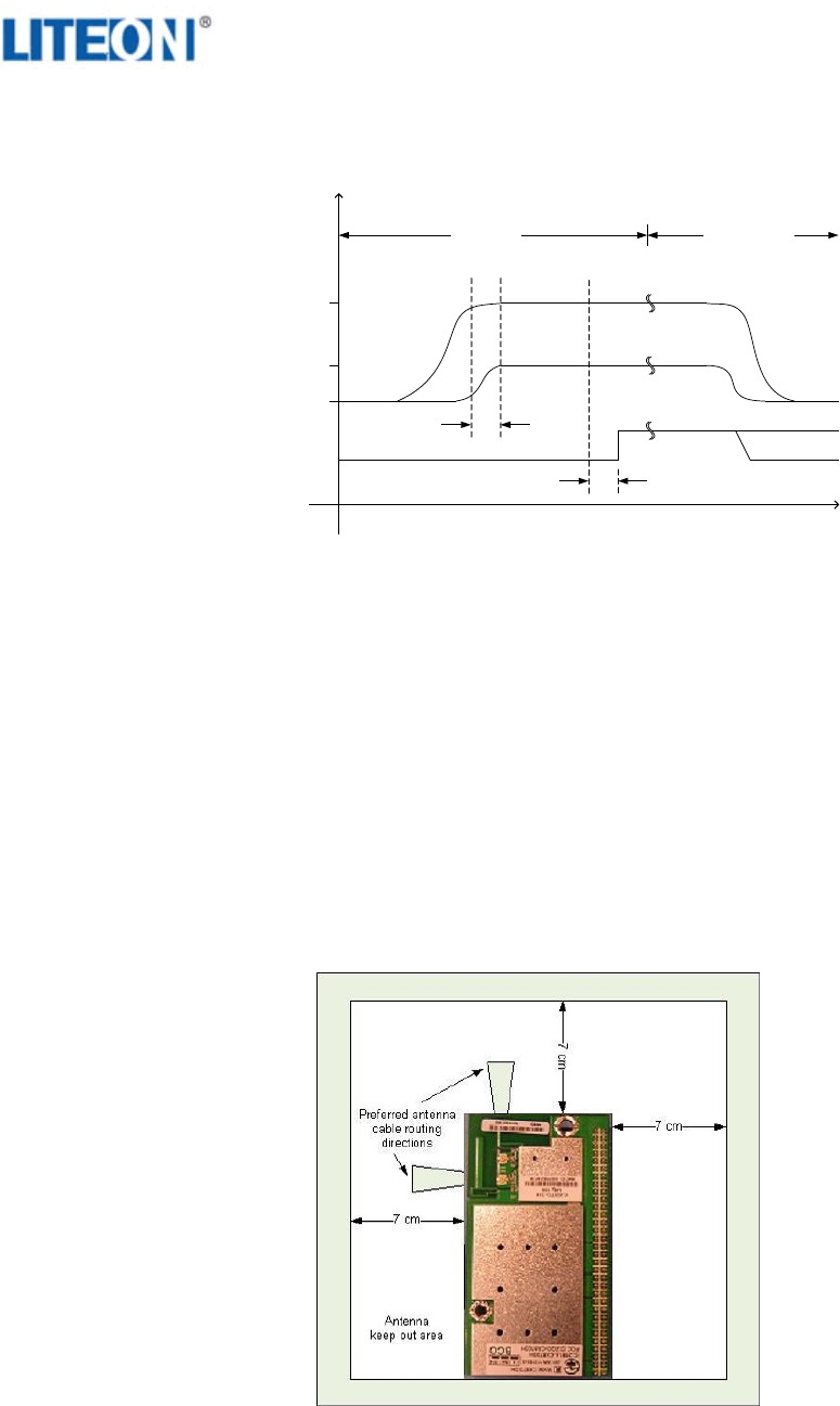
9.1.1 Power up, Reset and Power Down Timing
Time
Voltage
NRESET_MOD
0V
+1.2V
+3.3V
< 300ms
>= 2ms
Power Up Power Down
9.2 RF Considerations
Note that overall system, RF and WiFi performance is significantly affected by the product design, environment and the
application. It is the responsibility of the product designer to ensure proper system level shielding (if required) and to verify
performance and fitness for the given product features and applications.
The WiFi performance will be affected by the RF environment surrounding the CX module. Please ensure that the CX
module is positioned in a “quiet” RF environment, as far away as possible from high frequency clock signals and any other
sources of RF energy. Also, make sure the antenna is not shielded by any metal objects, for example loudspeakers or other
metal parts. Please make sure that the power supplies, in particular the +1.9V supply, are quiet and free from noise.
SMSC recommends that systems implementing AirPlay should use a module configuration that includes on-module
shielding, as well as paying particular attention to system configuration and shielding. In particular, SMSC is recommending
the use of the Bottom Shield versions of the modules, which allows greater freedom in antenna positioning.
Also, please see the SMSC Application Note:
SMSCAppNote - CX870_Antenna_Placement_V1_4.pdf
regarding antenna positioning guidelines.
Please see below picture for the recommended keep out area and cable routing for the antennas.
COMPANY CONFIDENTIAL
34
10 Revision Control
Revision
Date / Author
Details of Change
Reason for Change
V2.8
(093012)
Sept 30, 2012
/ SHs
Updated Section 4 Ordering Guide with 2 new
rows for CX870-3LB & CX870-3MB and moved
the row for CX870-3KB to be with them.
New SKUs available.
V2.8
(092412)
Sept 24, 2012
/ SHs
Updated cover page with new Microchip logo;
removed SMSC logo from header; removed
SMSC logo & address from legal text (page 2);
added info about Microchip to legal text;
updated © to 2012.
Microchip purchased SMSC.
Updated filename to
‘CX_Module_DS_Rev2-8_MM-DD-YY.pdf’.
Data covers all CX modules.
Removed CX860 from Section 7.4 Module
Weight.
No CX860 module available.
Updated left side of footer to ‘SMSC CX
Module’.
Data sheet is for all CX modules.
Updated title of Section 7.1.1 to ‘Top & Bottom
View of CX Module with Bottom Shield’.
Drawings are for all CX modules.
Updated title of Section 7.2.1 to ‘Side View of
CX Module with Bottom Shield except
CX870-3JB’.
Drawings are for all CX modules.
In Sections 3.1, 3.2, 3.2.1 & 3.2.2, updated
occurrences of ‘CX870’ to ‘CX Module’.
Pictures are for all CX modules.
Updated Section 4 Ordering Guide to remove
rows for CX870-3DB and CX870-3DBS, and
add a row for CX870-3KB.
Updated to show actual status.
Removed ‘I2C’ box, arrow & label in Section 2
Block Diagram.
Correction.
V2.8
(090912)
Sept 9, 2012 /
SHs
Updated Section 2 Block Diagram to show
obscured black lines leading out from LCD &
SSM blocks.
Correction.
In Section 2 Block Diagram changed “DM860A
or DM870A” to “DM870A or DM875”
CX module uses DM870A and DM875.
In Section 1 Introduction, changed “DM860A
and DM870A” to “DM870A and DM875”
CX module uses DM870A and DM875.
In Section 4 Ordering Guide, added a ‘Status’
column and status code key.
To show current availability status of each
module version.
In Section 4 Ordering Guide, added row for
CX875-3PB.
To give details of newly available module
version.
In Section 4 Ordering Guide, changed “SMSC
IC’s” heading to “SMSC ICs”.
Correction.
In Section 6.0.1 Antenna Considerations,
replaced text list with a new table.
Updated information and in a clearer format.
Added a new section 6.0.2 CX Power Settings
Used For Modular Approval.
To provide more details about CX module
power settings.
In Section 6 Regulatory Compliance and
Quality, updated the Compliance entry for New
Zealand / Australia for Radio Regulations from
“CE” to “AZ/NZS:4268”
Updated information.
In Section 9.2 RF Considerations, changed the
application note file path from “App Note
Antenna Placement recommendation CX870
modules rev1.1.pdf” to “SMSCAppNote -
CX870_Antenna_Placement_V1_4.pdf”
Provide most up to date Application Note file.
In Section 9.2 RF Considerations, added note &
picture regarding recommended keep out area
and cable routing for antennas.
Provide information about keep out areas and
cable routing.
In Notes of Section 8.2.1 Pin Descriptions,
added text regarding schematics being
compressed into zip files to Notes 4, 5 & 11.
Provide further information about schematic
files.
V2.7
June 13,
In Section 4 Ordering Guide, made rows for
All new designs should use modules with a

COMPANY CONFIDENTIAL
35
Revision
Date / Author
Details of Change
Reason for Change
(061312)
2012 / SHs
CX870-3B, 3H, 3I, 3J shaded.
bottom shield, so modules without a bottom
shield are now marked as "NOT TO BE USED
FOR NEW/STANDARD MP DESIGNS" by
shading the rows in the Ordering Guide table for
those modules with no bottom shield.
V2.6
(050812)
May 8, 2012 /
SHs
Removed entries in ‘8MByte NOR’ column for
modules 3A, 3B, 3D, 3DS in Section 4 Ordering
Guide
Correction.
V2.5
(042212)
April 22, 2012
/ SHs
Updated title of Section 7.2.1 Side View of
CX870 Module with Bottom Shield to include
“…except CX870-3JB”
Reflect addition of separate section (7.2.2) for
the CX870-3JB module.
Added Section 7.2.2 Side View of CX870
Module with Bottom Shield part number
CX870-3JB only
CX870-3JB has thinner bottom shield than other
modules.
V2.4
(032312)
March 23,
2012 / SHs
Added IC PIN entry for MIICRS in J3 Low
Density Connector table in Section 8.2.2
Connector PIN Assignments.
CX module uses DM870A.
Changed "MMIICRS" to "MIICRS" in Section
8.2.3 GPIO Assignments.
Correction.
Changed "MMIICRS" to "MIICRS" in J3 Low
Density Connector table in Section 8.2.2
Connector PIN Assignments.
Correction.
Changed "MMIICRS" to "MIICRS" in GPIO table
in Section 8.2.1 Pin Descriptions.
Correction.
Added important note text to Tx Power row in
Section 5.3 WiFi Specification.
To indicate which modules the Tx Power
specifications relate to.
Removed the ‘m’ from "+/-1dBm" in the Tx
Power row in Section 5.3 WiFi Specification.
Correction.
V2.4
(031712)
March 17,
2012 / SHs
In Section 5.3 WiFi Specifications, updated
Transmission Speed entry
Add missing 2Mbps speed.
In Section 4 Ordering Guide, changed all
occurrences of DM870 to DM870A & DM860 to
DM860A
CX module uses DM870A.
In Section 2 Block Diagram, changed all
occurrences of DM870 to DM870A & DM860 to
DM860A
CX module uses DM870A.
In Section 1 Introduction, changed all
occurrences of DM870 to DM870A & DM860 to
DM860A
CX module uses DM870A.
In Section 8.2.1 Pin Descriptions, changed all
occurrences of DM870 to DM870A
CX module uses DM870A.
In the Notes for Section 8.2.1 Pin Descriptions,
changed dat_DM870_16_datasheet.pdf to
DM870A DS rev. 1.3_12-15-11.pdf
CX module uses DM870A.
Changed all occurrences of DM870 to DM870A
throughout the datasheet.
CX module uses DM870A.
Updated J1, J2 & J3 tables in Section 8.2.2
Connector PIN Assignments, changing DM870
to DM870A.
CX module uses DM870A.
Changed "WiFi (on-module PCB diversity)"
column heading to "Internal PCB Diversity
Antennas" in Section 4 Ordering Guide
Improve clarity of meaning.
Added ‘FCC’ to North America in Frequency
Band entry in Section 5.3 WiFi Specification
Specify North American WiFi regulatory
certification body.
Updated TX EVM entry in Section 5.3 WiFi
Specifications
Update values to better reflect actual
performance.
Updated Rx Sensitivity entry in Section 5.3 WiFi
Specifications
Update values to better reflect actual
performance.
Updated Tx Power entry in Section 5.3 WiFi
Specifications
Show test conditions.
COMPANY CONFIDENTIAL
36
Revision
Date / Author
Details of Change
Reason for Change
V2.4
(031212)
March 12,
2012 / SHs
Added Section 3.6 Production Module with
Bottom shield (Part Numbers with a "B" after the
configuration letter)
Show module versions with bottom shield.
Added Section 3.6.1 Including J3 Low Density
64-pin connector - Bottom View
Show bottom shield.
Added Section 3.6.2 Including J2 High Density
120-pin connector - Bottom View
Show bottom shield.
V2.4
(031012)
March 10,
2012 / SHs
Updated Section 4 Ordering Guide & Section
4.1 Part Number Syntax drawing with bottom
shield versions
Bottom shield versions added to table and
Syntax drawing.
Added another note to Section 8.2.3 GPIO
Assignments
Document missing GPIOs for CX870-3K.
Updated TX Power row in Section 5.3 WiFi
Specification (CX870 only)
Show improved tolerances for TX power.
Added Section 7.1.1 Top & Bottom View of
CX870 Module with Bottom Shield
Show drawings of module with Bottom Shield.
Added Section 7.2.1 Side View of CX870
Module with Bottom Shield
Show drawings of module with Bottom Shield.
Added a note to Section 7.3 3D View of CX870
Module
To indicate availability of digital copy of 3D view
of module.
Added additional text to Section 9.2 RF
Considerations
Providing further recommendations regarding
the use of bottom shield versions and to indicate
the availability of a pdf about antenna
positioning guidelines.
V2.3
(112011)
November 20,
2011 / SHs
Added CX870-3DS option to Section 4 Ordering
Guide
To indicate soldered shield version.
V2.2
(110811)
November 8,
2011 / SHs
Added CX870-3K option to Section 4 Ordering
Guide.
Added -3K option.
V2.1
(100711)
October 7,
2011 / SHs
Updated title of Section 6.1 from “1 RoHS” to
“RoHS”.
Correcting typo.
In Section 10 Revision Control table, updated
an entry for V2.0 b in the Reason for Change
column from “RTV” to “RTC”
Correcting typo.
Removed “Preliminary Datasheet” from the
footer.
CX module is in production, so the datasheet is
no longer preliminary.
Removed the word “Preliminary” from the title
page.
CX module is in production, so the datasheet is
no longer preliminary.
V2.0
(100211)
October 2,
2011 / SHs
Updated Section 5.3 WiFi Specification “TX
Power” entry for 802.11g
Correspond to actual production test limits.
Updated Section 6.0.1 Antenna Considerations
with updated module numbering scheme
Revert to original module numbering scheme.
Updated Section 6.7 Module Quality with new
Defect Rate
Data is now available.
Updated Section 4.1 Part Number Syntax with
removal of Antenna Configuration number and
Note
Revert to original part numbering scheme.
Updated Section 10 Revision Control with new
Reason for Change column
Corporate standard.
V2.0
(092611)
Sept. 26,
2011 / SHs
Change from BridgeCo logos and disclaimer
text to SMSC logos and disclaimer text
Corporate standard.
Updated location of red boxes in Section 3.2.1
CX870 Bottom View with 64-pin Low density
connector
Improve alignment of red box to photo.
Updated location of red boxes in Section 3.2.2
CX870 Bottom View with 120-pin Media
connector
Improve alignment of red box to photo.
Moved Section 5.3 WiFi Specification on to one
page
Improve readability.
Updated Customer Portal information in Section
6 Regulatory Compliance and Quality
Easier to access URL directly.
Reverted Antenna Considerations back to
Section 6.0.1; subsequently all subsections in
Decided to keep original part numbering
scheme to avoid unnecessary paper work and
COMPANY CONFIDENTIAL
37
Revision
Date / Author
Details of Change
Reason for Change
Section 6 reverted back to original numbering
the need to redo certifications.
Updated Notes 11 & 12 in Section 8.2.1 Pin
Descriptions with updated Customer Portal
information
Easier to access URL directly.
Updated Table of Contents
Keep TOC aligned with actual content.
V2.0 c
Sept. 14,
2011 / SHs
Updated font styling of Table of Contents
Easier to read.
Update Section 2 Block Diagram : moved
RJ45+Transformer & USB Type A boxes inside
the drawing boundary
Improve accuracy of drawing.
Updated Section 5.3 WiFi Specification (CX870
only) TX Power Description entry
Align data with test limits.
Updated Section 5.3 WiFi Specification (CX870
only) Rx Sensitivity Description entry
Align data with test limits.
Updated Section 5.3 WiFi Specification (CX870
only) : add a Note underneath the table
Clarification of the possible effect of changing
the TX Power setting.
Updated Section 4 Ordering Guide : changed
CX870-3D row Two Ant entry from (X)* to X
Change to match final CX870-3D configuration.
Updated Section 4 Ordering Guide : removed
the two blank rows
Improve readability.
V2.0 b
Sept. 10,
2011 / SHs
Updated the Description for pin NCS3 in Section
8.2.1 Pin Descriptions
Update to align with actual use.
Updated Section 4 Ordering Guide : added gray
background to CX870-3F & CX870-3G
Internal antenna versions are not available until
performance issues are resolved.
Updated Section 4 Ordering Guide : removed
the 2 from A, H, I & J version Part Numbers
Decided to keep original part numbering
scheme to avoid unnecessary paper work and
the need to redo certifications.
Updated Section 4 Ordering Guide : split Ext.
Diversity Antennas column into two, added two
sub-columns “One Ant.” & “Two Ant.”, moved Xs
to correspond with correct sub-column
Show the number of external antenna
connections.
Updated Section 4 Ordering Guide : CX870-3D :
removed X from WiFi column
CX870-3D is not configured for internal
antenna.
Updated Section 4 Ordering Guide : updated +
Note text
Explained about one or two external antenna
options.
Updated Section 4 Ordering Guide : moved the
+ from Part Numbers column to Ext. Diversity
Antennas column
Proper link for "+" Note.
Updated Section 4 Ordering Guide : removed #
Note completely
Content now covered by "+" Note
Updated Section 4.1 Part Number Syntax :
Updated graphic
Explain antenna configuration field
Updated Section 4.1 Part Number Syntax :
Updated Note text
Explain about one or two antenna configuration.
Updated text in Section 8.1 WLAN UFL Antenna
Connector
Remove references to part numbering scheme
which includes the number of antennas, and
repeat advice to use two external antennas.
Removed RTC elements from Section 2 Block
Diagram
Support for RTC is removed.
Updated the Description for pin 3V3RTC in
Section 8.2.1 Pin Descriptions
Support for RTC is removed.
V2.0 a
August 22,
2011 / SHs
Added Section 3.5 Example Production Module
Showing Soldered RF Shield
Photo shows that RF shield is soldered, needed
for Japan Telec certification.
V2.0
August 12,
2011 / SHs
Updated Note Section 4.1 Part number syntax
Highlighted that CX870-3D does not follow the
new part numbering scheme. This Note was
subsequently deleted, so this is not relevant any
more.
Updated all Section 3 Board Pictures to new
versions + inserted new Sections 3.2.1 & 3.2.2
which show two different bottom views
Improve accuracy of data sheet photos.
V1.9 c
August 2,
2011 / SHs
Updated Key Features on Title page:
removed (optional) from “WiFi-certified
802.11b/g” entry

COMPANY CONFIDENTIAL
38
Revision
Date / Author
Details of Change
Reason for Change
Updated Antenna Configuration entry in
Section 4.1 Part number syntax
V1.9 b
July 28, 2011
/ SHs
Updated Section 4.1 Part number syntax
o Updated graphic
o Added a Note
Changed intro text in Section 3 Board
Pictures
Updated Section 4 Ordering Guide
o Changed CX870-3B1 to
CX870-3B
o Updated the text for + note
o Added a note to CX870-3B Ext.
Diversity Antenna column
o Added a new # note
Added Section 6.0.1 Antenna
Considerations
V1.9 a
July 25, 2011
/ SHs
Inserted new photo for Section 3.1 Top
View of CX870
Inserted new photo for Section 3.2 Bottom
View of CX870
Added new Section 3.3 Production Module
with Top & RF shields
Added new Section 3.4 Production Module
with 64-pin Connector Option
Updated Section 4 Ordering Guide
o Added gray background to
CX870-3D
o Changed CX870-3A to
CX870-3A2
o Changed CX870-3B to
CX870-3B1
o Changed CX870-3H to
CX870-3H2
o Changed CX870-3I to
CX870-3I2
o Changed CX870-3J to
CX870-3J2
o Added a Note to the Part
Number title
Updated Section 8.1 WLAN UFL Antenna
Connector with new text
Updated Section 5.3 WiFi Specification TX
EVM entry to
-9dB@6MHz
Updated Section 6 Regulatory Compliance
& Quality with Module Versions Passed for
Radio Regulations entries
Replaced the Note in Section 6 to be main
body text and updated the text.
Added new Section 4.1 Part number
syntax
Updated module weight to 20g
V1.8 a
July 10, 2011
/ SHs
Update section 8.1 WLAN UFL Antenna
Connector
Deleted section 8.1.1 Coaxial antenna
connector dimensions
V1.8
July 5, 2011 /
SHs
Updated the acceptable surface-mount
receptacle parts in Section 8.1 WLAN UFL
Antenna Connector
COMPANY CONFIDENTIAL
39
Revision
Date / Author
Details of Change
Reason for Change
Added Appendix 1: Certification Notices
V1.7 c
May 13, 2011
/ SHs
Updated “Module Quality” Defect Rate
field entry
Updated “Board Dimensions & Weight”
drawings
Updated the “Electrical Specifications”
table
Added another Note to the “Pin
Descriptions” section
V1.7 b
May 11, 2011
/ SHs
Updated Note 8 in “Pin Descriptions” table
Re-imported “Board Dimensions &
Weight” drawings
Updated “Board Pictures” images
Updated board photo on Cover page
Updated the Feature list on Cover page
Updated J1, J2 & J3 “Connector PIN
Assignments” tables: removed Power
column & re-organised columns
Changed “Application Notes” title to
“Application Guidelines”
Updated Copyright date to “2011”
Updated Table of Contents font styling
V1.7 a
May 6, 2011 /
SHs
Re-imported Block Diagram as a wmf file
Updated “Power up, Reset & Power down
Timing” figure
Updated “Pin Descriptions” table
Re-organised text in “Power Supply
sequencing & Reset Timing”
Re-imported J2 & J3 Connector PIN
Assignment tables
V1.7
May 4, 2011 /
SHs
Added note to Module Weight section
Updated the Ordering Guide – Part
Numbers & added new J version
Added new text to the Board Pictures
section
Updated all Mechanical Drawings and
added & removed Notes
Updated the J3 Low Density Connector
table
Updated the GPIO Assignment table
Added new Power Supply & Timing figure
Updated the text in the “Power Supply
sequencing and Reset Timing” section
Updated the Key Connections table
Updated “Key Connections” section title to
“Pin Descriptions”
Updated “Detailed Connector PIN
Descriptions” section title to “Connector
PIN Assignments”
Updated J2 Media Connector table
V1.6 d
March 3,
2011 / SHs
Updated J3 Low Density Connector table
Update GPIO Assignments section and
table
V1.6 c
February 24,
2011 / SHs
Updated all mechanical drawings in
“Board Dimensions and Weights” section
Deleted warning note in “Board
Dimensions and Weights” section
COMPANY CONFIDENTIAL
40
Revision
Date / Author
Details of Change
Reason for Change
V1.6 b
February 23,
2011 / SHs
Updated “J3-Low density connector” pin
description table
Updated “GPIO Assignments” table
V1.6
February 11,
2011 / SHs
Entirely updated the “Ordering Guide”
Added a Note to the “Ordering Guide”
Updated the subsection titles for the
“Board Pictures” section
Updated the Block Diagram – changed
‘WiFi Antenna’ to ‘Ext. Antenna’
V1.5 b
January 27,
2011 / SHs
Added Note to “Board Dimensions and
Weight” section
V1.5 a
January 24,
2011 / SHs
Updated the “Ordering Guide” – removed
Mfg column and consolidated into one
table
Updated the Header to reflect Preliminary
nature of datasheet
V1.5
January 22,
2011 / SHs
Updated the datasheet to be a Preliminary
Datasheet
Added new feature to Summary on Front
Page
Updated “J3 - Low Density Connector”
table
Updated “GPIO Assignments” table
Added note to “Board Dimensions &
Weight – Side Views of CX870 module”
section
Updated text in “Application Notes –
Power Supply Sequencing & Reset
Timing” section
Updated “Block Diagram”
Updated text in “Connectors &
Connections – WLAN UFL Antenna
Connector” section
V1.4 b
January 11,
2011 / SHs
Updated the Application Notes, RF
Considerations section
V1.4
January 3,
2011 / SHs
Updated the module photo on the Title
page
Updated the Application Notes, RF
Considerations section
V1.3
December 23,
2010 / SHs
Updated Ordering Guide
Added Notes to Ordering Guide
Updated Block Diagram
Updated “J3 – Low Density Connector”
table
Updated “Electrical Specifications” table
Added Power Consumption data to
“Electrical Specifications” table
Updated the Board Dimensions and
Weight images
Updated the “GPIO Assignments” table
Added another Application Note
Added titles to Application Notes
V1.2
December 19,
2010 / SHs
Inserted CX860 and CX870 Module
Weights
Updated module image on Front Page
V1.1
December 13,
2010 / SHs
Added the Ordering Guide.
Updated the Block Diagram.
COMPANY CONFIDENTIAL
41
Revision
Date / Author
Details of Change
Reason for Change
Updated the “Electrical Specifications”
table
Updated the “Absolute Maximum Ratings”
table
Updated the Notes for “Regulatory
Compliance and Quality” section
Updated “Key Connections” table
Updated “J2 – Media Connector” table
Updated “J3 – Low Density Connector”
table
Updated “GPIO Assignments” table
Added Board Pictures
Replaced Mechanical Drawings in “Board
Dimensions and Weight” section
V1.0
October 18,
2010 / SHs
Initial Version
COMPANY CONFIDENTIAL
42
Part2. Antenna Spec Sheet
1 RFDPA870930IMAB301
COMPANY CONFIDENTIAL
43
2 RFDPA870945IMAB301