LITE ON TECHNOLOGY WCBN3510A 802.11 a/b/g/n/ac 2T2R+BT V4.2LE combo module User Manual LiteOn Technology Corp
LITE-ON Technology Corp. 802.11 a/b/g/n/ac 2T2R+BT V4.2LE combo module LiteOn Technology Corp
Contents
- 1. User Manual
- 2. User Manaul
- 3. User manual
User Manaul

Page 1/18
PRODUCT SPECIFICATION
Wi-Fi (11a/b/g/n/ac 2Tx2R)+BT (V4.2LE) SDIO Combo Module
WCBN3510A
User Manual
Page 2/18
CONTENT
DESCRIPTION ............................................................................................................................. 8
PRODUCT FEATURES ............................................................................................................... 8
PRODUCT SPECIFICATIONS ................................................................................................... 9
MAIN CHIPSET ................................................................................................................................. 9
FUNCTIONAL SPECIFICATIONS .......................................................................................................... 9
RECOMMENDED OPERATION CONDITIONS .................................................................... 12
PIN ASSIGMENT ....................................................................................................................... 12
MECHANICAL .......................................................................................................................... 14
FOOTPRINT .............................................................................................................................. 14
MODULE PINOUT .................................................................................................................... 15
BLOCK DIAGRAM ................................................................................................................... 15
MHF4 CONNECTOR SPEC ...................................................................................................... 16
POWER-UP SEQUENCE TIMING ........................................................................................... 17
EEPROM INFORMATION ....................................................................................................... 18
BT ................................................................................................................................................. 18
WI-FI ............................................................................................................................................ 18
ENVIRONMENTAL .................................................................................................................. 18
OPERATING .................................................................................................................................... 18
STORAGE ....................................................................................................................................... 18

Page 3/18
FCC Statement:
Federal Communication Commission Interference Statement
This equipment has been tested and found to comply with the limits for a Class B digital
device, pursuant to Part 15 of the FCC Rules. These limits are designed to provide reasonable
protection against harmful interference in a residential installation. This equipment generates,
uses and can radiate radio frequency energy and, if not installed and used in accordance with
the instructions, may cause harmful interference to radio communications. However, there is
no guarantee that interference will not occur in a particular installation. If this equipment
does cause harmful interference to radio or television reception, which can be determined by
turning the equipment off and on, the user is encouraged to try to correct the interference by
one of the following measures:
˗ Reorient or relocate the receiving antenna.
˗ Increase the separation between the equipment and receiver.
˗ Connect the equipment into an outlet on a circuit different from that to which the receiver
is connected.
˗Consult the dealer or an experienced radio/TV technician for help.
FCC Caution: Any changes or modifications not expressly approved by the party responsible
for compliance could void the user’s authority to operate this equipment.
This device complies with Part 15 of the FCC Rules. Operation is subject to the following two
conditions: (1) This device may not cause harmful interference, and (2) this device must
accept any interference received, including interference that may cause undesired operation.
For product available in the USA/Canada market, only channel 1~11 can be operated.
Selection of other channels is not possible.
This device and its antenna(s) must not be co-located with any other transmitters except in
accordance with FCC multi transmitter product procedures.
Referring to the multi transmitter policy, multiple transmitter(s) and module(s) can be
operated simultaneously without C2PC.
IMPORTANT NOTE:
FCC Radiation Exposure Statement:
This equipment complies with FCC radiation exposure limits set forth for an uncontrolled
environment. This equipment should be installed and operated with minimum distance 20 cm
between the radiator & your body.

Page 4/18
IMPORTANT NOTE:
This module is intended for OEM integrator. The OEM integrator is responsible for the
compliance to all the rules that apply to the product into which this certified RF module is
integrated.
Additional testing and certification may be necessary when multiple modules are used.
20 cm minimum distance has to be able to be maintained between the antenna and the users
for the host this module is integrated into. Under such configuration, the FCC radiation
exposure limits set forth for an population/uncontrolled environment can be satisfied.
Any changes or modifications not expressly approved by the manufacturer could void the
user's authority to operate this equipment.
USERS MANUAL OF THE END PRODUCT:
In the users manual of the end product, the end user has to be informed to keep at least 20
cm separation with the antenna while this end product is installed and operated. The end
user has to be informed that the FCC radio frequency exposure guidelines for an uncontrolled
environment can be satisfied. The end user has to also be informed that any changes or
modifications not expressly approved by the manufacturer could void the user's authority to
operate this equipment. If the size of the end product is smaller than 8x10cm, then additional
FCC part 15.19 statement is required to be available in the users manual: This device complies
with Part 15 of FCC rules. Operation is subject to the following two conditions: (1) this device
may not cause harmful interference and (2) this device must accept any interference received,
including interference that may cause undesired operation.
LABEL OF THE END PRODUCT:
The final end product must be labeled in a visible area with the following " Contains TX FCC ID:
PPQ- WCBN3510A ". If the size of the end product is larger than 8x10cm, then the following
FCC part 15.19 statement has to also be available on the label: This device complies with Part
15 of FCC rules. Operation is subject to the following two conditions: (1) this device may not
cause harmful interference and (2) this device must accept any interference received,
including interference that may cause undesired operation.
OEM Integrator Checklist
The party below will implement the LITE-ON Module in host systems in accordance with the
instructions specified in this document and the documents referenced herein.
1. The OEM integrator will ensure the Module is integrated in a host systems using only the
approved antenna model(s) described in this document.
2. The OEM integrator will ensure the antenna placement inside the host system will

Page 5/18
maintain the required spacing to end user for RF Exposure compliance, as specified in this
document.
3. If other radios are integrated inside the host with the LITE-ON Module, the OEM
integrator will contact its test lab, TCB or LITE-ON to determine if additional FCC
compliance evaluation is required to meet FCC collocation rules.
4. The OEM integrator will ensure end user documentation will contain the specified
regulatory wording and ensure the host system and the Module itself are labeled as
specified in this document.
5. The OEM integrator will ensure the Module is programmed in the factory with compliant
transmit power not exceeding the levels specified in this document.
LITE-ON requests that the OEM integrator acknowledge its receipt of this document and the
above instructions. You may contact LITE-ON with any questions concerning this document or
the responsibilities of the OEM integrator.
IC Statement:
This device complies with Industry Canada license exempt RSS standard(s). Operation is
subject to the following two conditions: (1) this device may not cause interference, and (2)
this device must accept any interference, including interference that may cause undesired
operation of the device.
Le présent appareil est conforme aux CNR d'Industrie Canada applicables aux appareils radio
exempts de licence. L'exploitation est autorisée aux deux conditions suivantes : (1) l'appareil
ne doit pas produire de brouillage, et (2) l'utilisateur de l'appareil doit accepter tout
brouillage radioélectrique subi, même si le brouillage est susceptible d'en compromettre le
fonctionnement.
For product available in the USA/Canada market, only channel 1~11 can be operated.
Selection of other channels is not possible.
Pour les produits disponibles aux États Unis / Canada du marché, seul le canal 1 à 11 peuvent
être exploités. Sélection d'autres canaux n'est pas possible.
This device and its antenna(s) must not be co-located with any other transmitters except in
accordance with IC multi transmitter product procedures.
Referring to the multi transmitter policy, multiple transmitter(s) and module(s) can be
operated simultaneously without reassessment permissive change.
Cet appareil et son antenne (s) ne doit pas être co-localisés ou fonctionnement en association
avec une autre antenne ou transmetteur.
The device for operation in the band 5150-5250 MHz is only for indoor use to reduce the

Page 6/18
potential for harmful interference to co-channel mobile satellite systems.
les dispositifs fonctionnant dans la bande 5150-5250 MHz sont réservés uniquement pour
une utilisation à l’intérieur afin de réduire les risques de brouillage préjudiciable aux systèmes
de satellites mobiles utilisant les mêmes canaux.
The maximum antenna gain permitted for devices in the band 5725-5850 MHz shall be such
that the equipment still complies with the e.i.r.p. limits specified for point-to-point and
Non-point-to-point operation as appropriate.
le gain maximal d’antenne permis (pour les dispositifs utilisant la bande 5725-5850 MHz)
doit se conformer à la limite de p.i.r.e. spécifiée pour l’exploitation point à point et non-point
à point, selon le cas.
Dynamic Frequency Selection (DFS) for devices operating in the bands 5250- 5350 MHz,
5470-5600 MHz and 5650-5725 MHz.
Sélection dynamique de fréquences (DFS) pour les dispositifs fonctionnant dans les bandes
5250-5350 MHz, 5470-5600 MHz et 5650-5725 MHz.
The maximum antenna gain permitted for devices in the bands 5250-5350 MHz and
5470-5725 MHz shall be such that the equipment still complies with the e.i.r.p. limit.
le gain maximal d’antenne permis pour les dispositifs utilisant les bandes 5250-5350 MHz et
5470-5725 MHz doit se conformer à la limite de p.i.r.e.
Users should also be advised that high power radars are allocated as primary users (i.e.
priority users) of the bands 5250-5350 MHz and 5650-5850 MHz and that these radars could
cause interference and/or damage to LE•LAN devices.
De plus, les utilisateurs devraient aussi être avisés que les utilisateurs de radars de haute
puissance sont désignés utilisateurs principaux (c.•à•d., qu’ils ont la priorité) pour les bandes
5250-5350 MHz et 5650-5850 MHz et que ces radars pourraient causer du brouillage et/ou
des dommages aux dispositifs LAN•EL.
Pour une utilisation en intérieur uniquement.

Page 7/18
IMPORTANT NOTE:
IC Radiation Exposure Statement:
This equipment complies with IC RSS-102 radiation exposure limits set forth for an
uncontrolled environment. This equipment should be installed and operated with minimum
distance 20 cm between the radiator & your body.
Cet équipement est conforme aux limites d'exposition aux rayonnements IC établies pour un
environnement non contrôlé. Cet équipement doit être installé et utilisé avec un minimum de
20 cm de distance entre la source de rayonnement et votre corps.
This module is intended for OEM integrator. The OEM integrator is still responsible for the IC
compliance requirement of the end product, which integrates this module.
Any changes or modifications not expressly approved by the manufacturer could void the
user's authority to operate this equipment.
USERS MANUAL OF THE END PRODUCT:
In the users manual of the end product, the end user has to be informed to keep at least 20
cm separation with the antenna while this end product is installed and operated. The end
user has to be informed that the IC radio-frequency exposure guidelines for an uncontrolled
environment can be satisfied. The end user has to also be informed that any changes or
modifications not expressly approved by the manufacturer could void the user's authority to
operate this equipment. Operation is subject to the following two conditions: (1) this device
may not cause harmful interference and (2) this device must accept any interference received,
including interference that may cause undesired operation.
LABEL OF THE END PRODUCT:
The final end product must be labeled in a visible area with the following " Contains TX IC:
4491A-WCBN3510A ".

Page 8/18
DESCRIPTION
QCA9379-3 is a single-die wireless local area network(WLAN) and Bluetooth(BT) combo
solution to support 2x2 MIMO with two spatial streams IEEE802.11 a/b/g/n/ac WLAN
standards and BT 4.2+HS enabling seamless integration of WLAN/BT and Low Energy
technology.
PRODUCT FEATURES
Bluetooth V4.2 LE system
Backwards compatible with BT version of 1.1, 1.2, 2.0, 2.1, 3.0+HS and V4.0LE
Bluetooth Class I transmission power
Support for Adaptive Frequency Hopping(AFH), Secure Simple Pairing (SSP) and
Extended Inquiry Response (EIR) function
Scatternet operation with up to four active piconets with background scan and support
for scatter mode
Low power consumption for meeting worldwide energy standards
Operate at ISM frequency Band (2.4/5GHz)
IEEE Standards Support, 802.11a ,802.11b, 802.11g 802.11n and 802.11ac
Support for both 20 MHz/40 MHz channel width in 2.4GHz and 20 MHz/40
MHz/80MHz channel width in 5GHz
Enterprise level security supporting: WPS2.0,WAPI, WPA, WPA2
Dual-stream IEEE 802.11n support for 20MHz and 40MHz channels provides PHY
layer rates up to 300Mbps
Dual-stream IEEE 802.11ac support for 80MHz channels provides PHY layer rates up
to 867Mbps
Support for WI-Fi Direct
Support MU-MIMO
Fully compliance with SDIO v3.0 specification
Support OS: Linux based
RoHS compliance
Low Halogen compliance
Page 9/18
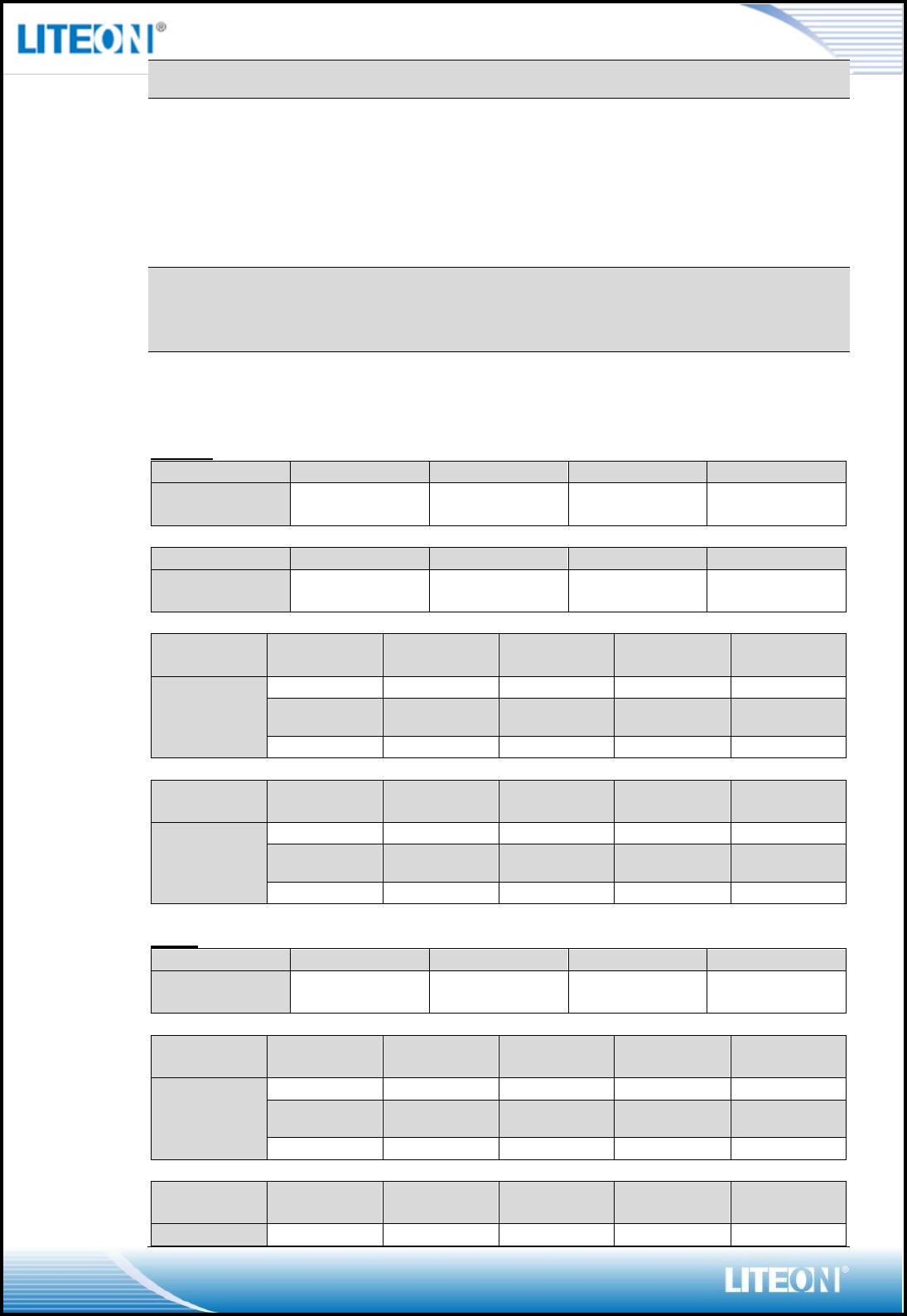
PRODUCT SPECIFICATIONS
MAIN CHIPSET
Qualcomm Atheros QCA9379-3
FUNCTIONAL SPECIFICATIONS
BT Function
Standard
Bluetooth V4.2LE
Bus Interface
UART
Data Rate
1 Mbps, 2Mbps and Up to 3.2Mbps
Modulation Scheme
GFSK, π/4-DQPSK and 8-DPSK
Frequency Range
2.402~2.480 GHz
Transmit Output
Power
+4 ≤ Output Power ≤ +10dBm; Class I Device
Receiver Sensitivity
< 0.1% BER at -94dBm
Wi-Fi Function
Standard
IEEE802.11a; IEEE802.11b; IEEE 802.11g; IEEE 802.11n;
IEEE802.11ac
Bus Interface
SDIO 3.0
Data Rate
802.11a:
54, 48, 36, 24, 18, 12, 9, 6 Mbps
802.11b:
11, 5.5, 2, 1 Mbps
802.11g:
54, 48, 36, 24, 18, 12, 9, 6 Mbps
802.11n:
MCS 0 to 15 for HT20MHz
MCS 0 to 15 for HT40MHz
802.11ac:
MCS 0 to 8 for HT20MHz
MCS 0 to 9 for HT40MHz
MCS 0 to 9 for HT80MHz
Media Access Control
CSMA/CA with ACK
Modulation Technique
802.11a:
64QAM, 16QAM, QPSK, BPSK
802.11b:
CCK, DQPSK, DBPSK
802.11g:
64QAM, 16QAM, QPSK, BPSK
802.11n:
64QAM, 16QAM, QPSK, BPSK
802.11ac:
256QAM, 64QAM, 16QAM, QPSK, BPSK
Page 10/18
Network Architecture
Infrastructure mode
Operation Channel
2.4GHz
11: (Ch. 1-11) – United States
13: (Ch. 1-13) – Europe
14: (Ch. 1-14) – Japan
5GHz
21: USA
19: EU
8: Japan
Frequency Range
802.11bg
2.400 ~ 2.4835 GHz
802.11a
5.15 ~ 5.85 GHz
Transmit Output Power - single chain @ant;
Tolerance: ±2dBm@2.4GHz; ±2.5dBm@5GHz
2.4GHz
802.11b
1Mbps
2Mbps
5.5Mbps
11Mbps
Tgtpwr
(dBm)
14.5
14.5
14.5
14.5
802.11g
6~24Mbps
36Mbps
48Mbps
54Mbps
Tgtpwr
(dBm)
16.5
16
15
13.5
802.11n
HT20
MCS0
MCS1
MCS2
MCS3
MCS4
Tgtpwr
(dBm)
16.5
16.5
16.5
16
16
MCS5
MCS6
MCS7
MCS8
MCS9
15
14
13.5
11.5
802.11n
HT40
MCS0
MCS1
MCS2
MCS3
MCS4
Tgtpwr
(dBm)
15.5
15.5
15.5
15
15
MCS5
MCS6
MCS7
MCS8
MCS9
14
13
12.5
11.5
10.5
5GHz
802.11a
6~24Mbps
36Mbps
48Mbps
54Mbps
Tgtpwr
(dBm)
15.5
14
13
12
802.11n
HT20
MCS0
MCS1
MCS2
MCS3
MCS4
Tgtpwr
(dBm)
15.5
15.5
15.5
15
15
MCS5
MCS6
MCS7
MCS8
MCS9
14
13
12
11
802.11n
HT40
MCS0
MCS1
MCS2
MCS3
MCS4
Tgtpwr
14.5
14.5
14.5
14
14
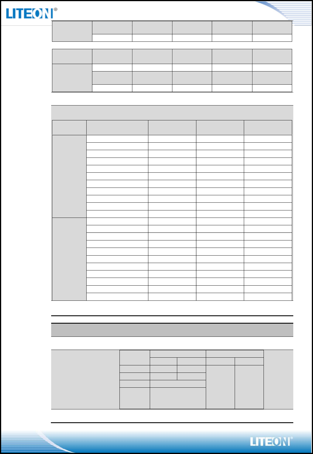
Page 11/18
(dBm)
MCS5
MCS6
MCS7
MCS8
MCS9
13
12
11
10
9
802.11ac
VHT80
MCS0
MCS1
MCS2
MCS3
MCS4
Tgtpwr
(dBm)
13.5
13.5
13.5
13
13
MCS5
MCS6
MCS7
MCS8
MCS9
12
11
10
9
8
Receiver Sensitivity
Frequency
Band
Rate
Condition
1x1(1SS)
(dBm)
2x2(1SS)
(dBm)
2.4G
11b-1M
PER < 8%
-95
-97
11b-11M
PER < 8%
-87
-87
11g-6M
PER < 10%
-90
-92
11g-54M
PER < 10%
-73
-75
11ac-VHT20MCS0
PER < 10%
-89.5
-91.5
11ac-VHT20MCS7
PER < 10%
-73
-75
11ac-VHT20MCS8
PER < 10%
-68
-70
11ac-VHT40MCS0
PER < 10%
-87
-89
11ac-VHT40MCS7
PER < 10%
-69.5
-71.5
11ac-VHT40MCS8
PER < 10%
-66.5
-68.5
11ac-VHT40MCS9
PER < 10%
-63
-66
5G
11a-6M
PER < 10%
-87.5
-89.5
11a-54M
PER < 10%
-71
-73
11ac-VHT20MCS0
PER < 10%
-87.5
-89.5
11ac-VHT20MCS7
PER < 10%
-70
-73
11ac-VHT20MCS8
PER < 10%
-66
-69
11ac-VHT40MCS0
PER < 10%
-84.5
-86.5
11ac-VHT40MCS7
PER < 10%
-67
-69
11ac-VHT40MCS9
PER < 10%
-61
-64
11ac-VHT80MCS0
PER < 10%
-81.5
-83.5
11ac-VHT80MCS7
PER < 10%
-65
-67
11ac-VHT80MCS9
PER < 10%
-57
-60
Security
WPS, WPA, WPA2, WEP 64bit & 128bit, IEEE 802.1X, IEEE
802.11i
Common Function
Operating Voltage
3.3 V ±5% I/O supply voltage
Power Consumption
Mode
Average
Peak
2.4G
5G
2.4G
5G
TX
RX
Disable
WiFi+BT
@Wake
up mode
Antenna Type
Triple MHF4 Antenna connectors for WiFi/BT
Page 12/18
RECOMMENDED OPERATION CONDITIONS
Symbol
Parameter
Min
Typ
Max
Units
VDD33
3.3V Supply Voltage
3.14
3.3
3.46
V
VDD33_SWREG_VIN
Supply Voltage for internal PMU
3.14
3.3
3.46
V
VDDIO_GPIO0
VDDIO_GPIO1
VDDIO_GPIO2
VDDIO_AO_IN
Voltage supply for all IO signals
1.71
3.14
1.8
3.3
1.89
3.46
V
AVDD11
1.1V supply from internal 1.1V
PMU
1.05
1.1
1.2
V
PIN ASSIGMENT
* The following signal type is defined:
I: Input; O: Output; I/O: Input/Output; G: Ground
Pin.
Pin Define
I/O
Description
Status
1
GND
G
Ground
YES
2
AVDD11
I
Analog 1.1V input from Pin#28 of Module
(Host no need to connect)
NC
3
GND
G
Ground
YES
4
VDD33_WL_PA1
I
3.3V Power for both 2.4GHz/5GHz PA in
WLAN Chain 1
YES
5
VDD33
I
3.3V power for WLAN
YES
6
GND
G
Ground
YES
7
VDDIO_XTAL
I
Share same voltage of VDDIO_AO_IN
(Pin#32)
YES
8
BT_UART_CTS
I
UART Clear to Send for BT interface
YES
9
BT_UART_TXD
O
UART Transmit Data for BT interface
YES
10
HOST_WAKEUP_BT#
I
Host wake up BT of QCA9379-3, Low Active
YES
11
BT_UART_RXD
I
UART Receive Data for BT interface
YES
12
BT_PCM_SYN
I
PCM synchronous for BT
YES
13
BT_PCM_OUT
O
PCM Data out for BT
YES
14
BT_UART_RTS
O
UART Ready to Send for BT interface
YES
15
BT_PCM_CLK
I
PCM Clock for BT
YES
16
AVDD11
I
Analog 1.1V input from Pin#28 of Module
(Host no need to connect)
NC
17
BT_PCM_IN
I
PCM Data in for BT. 10K PU in the module
YES
18
VDDIO_GPIO1
I
1.8V or 3.3V upon signal interface
YES
19
RESERVED
NC
20
RESERVED
NC
21
VDDIO_GPIO0
I
Can be 1.8V (SDIO3.0) or 3.3V (SDIO2.0)
YES
22
SDOI_DATA3
I/O
SDIO Data Line3 for WLAN
YES
23
WOW#
O
WLAN wake up Host, Low Active
YES
24
SDIO_CLK
I
SDIO Clock for WLAN
YES
Page 13/18
25
SDOI_DATA2
I/O
SDIO Data Line2 for WLAN
YES
26
SDOI_DATA1
I/O
SDIO Data Line1 for WLAN
YES
27
SDOI_DATA0
I/O
SDIO Data Line0 for WLAN
YES
28
AVDD11
O
Analog 1.1V output
(Host no need to connect)
NC
29
SDIO_CMD
I/O
SDIO Command for WLAN
YES
30
WLAN_EN#
I
Active low to reset WLAN
YES
31
BT_EN#
I
Active low to reset BT
YES
32
VDDIO_AO_IN
I
Can be 1.8V or 3.3V to support always on
circuit of QCA9379-3. This signal must be
connected to 1st power on and last power off
power rail. The design is target to connect to
3.3V
YES
33
BT_WAKEUP_HOST#
O
BT wake up Host. 10K PU in the module
, Low Active
YES
34
Debug_UART_TXD
O
Firmware Debug pin, Host can be not
connected
NC
35
Debug_UART_RXD
I
Firmware Debug pin, Host can be not
connected
NC
36
VDD33_SWREG_VIN
I
3.3V input to internal SWREG PMU and
OTPREG PMU
YES
37
SWREG_GND
G
Ground
YES
38
SWREG_GND
G
Ground
YES
39
VDDIO_GPIO2
I
1.8V or 3.3V upon signal interface
YES
40
32.768KHz_IN
I
Optional external low-power 32.768KHz
input Signal can not be active before
VDDIO_GPIO2 is applied
YES
41
AVDD11
I
Analog 1.1V input from Pin#28 of Module
(Host no need to connect)
NC
42
GND
G
Ground
YES
43
GND
G
Ground
YES
44
GND
G
Ground
YES
45
GND
G
Ground
YES
46
VDD33
I
3.3V Power for BT PA
YES
47
VDD33
I
3.3V Power for both 2.4GHz/5GHz PA in
WLAN Chain 0
YES
48
GND
G
Ground
YES
49
AVDD11
I
Analog 1.1V input from Pin#28 of Module
(Host no need to connect)
NC
50~66
GND
G
Ground
YES
Page 14/18
MECHANICAL
FOOTPRINT
Page 15/18
MODULE PINOUT
BLOCK DIAGRAM
Page 16/18
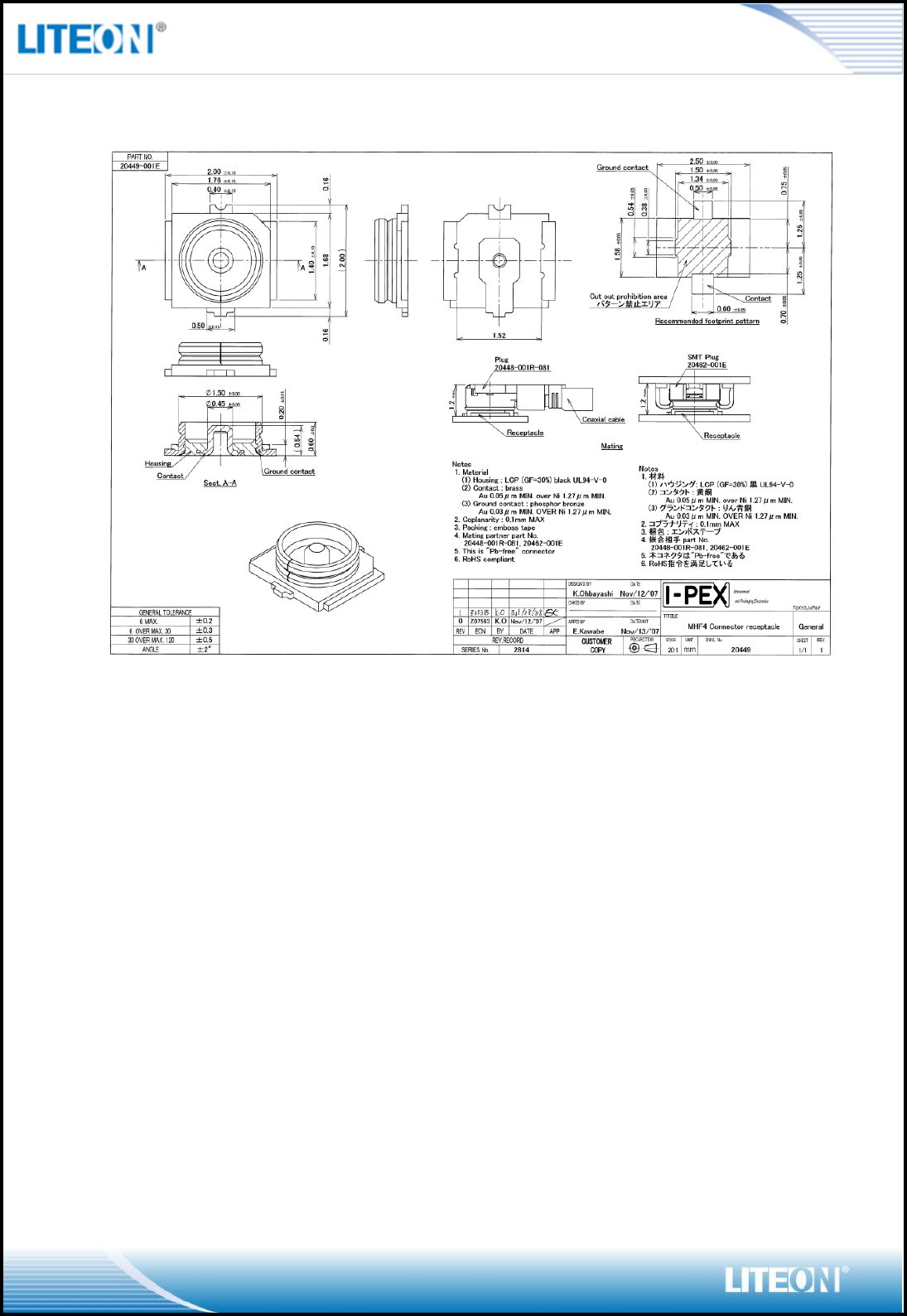
MHF4 CONNECTOR SPEC
Page 17/18
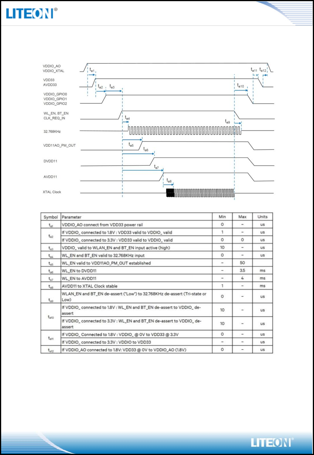
POWER-UP SEQUENCE TIMING
Page 18/18
EEPROM INFORMATION
BT
Vendor ID
0x0271
Product ID
0x0801
WI-FI
Reg Domain
TBD
Vendor ID
0x0271
Product ID
0x0801
ENVIRONMENTAL
OPERATING
Operating Temperature: 0 to 50 C (32 to 122 F)
Relative Humidity: 5-90% (non-condensing)
STORAGE
Temperature: -40 to 80 C (-40 to 176 F)
Relative Humidity: 5-95% (non-condensing)