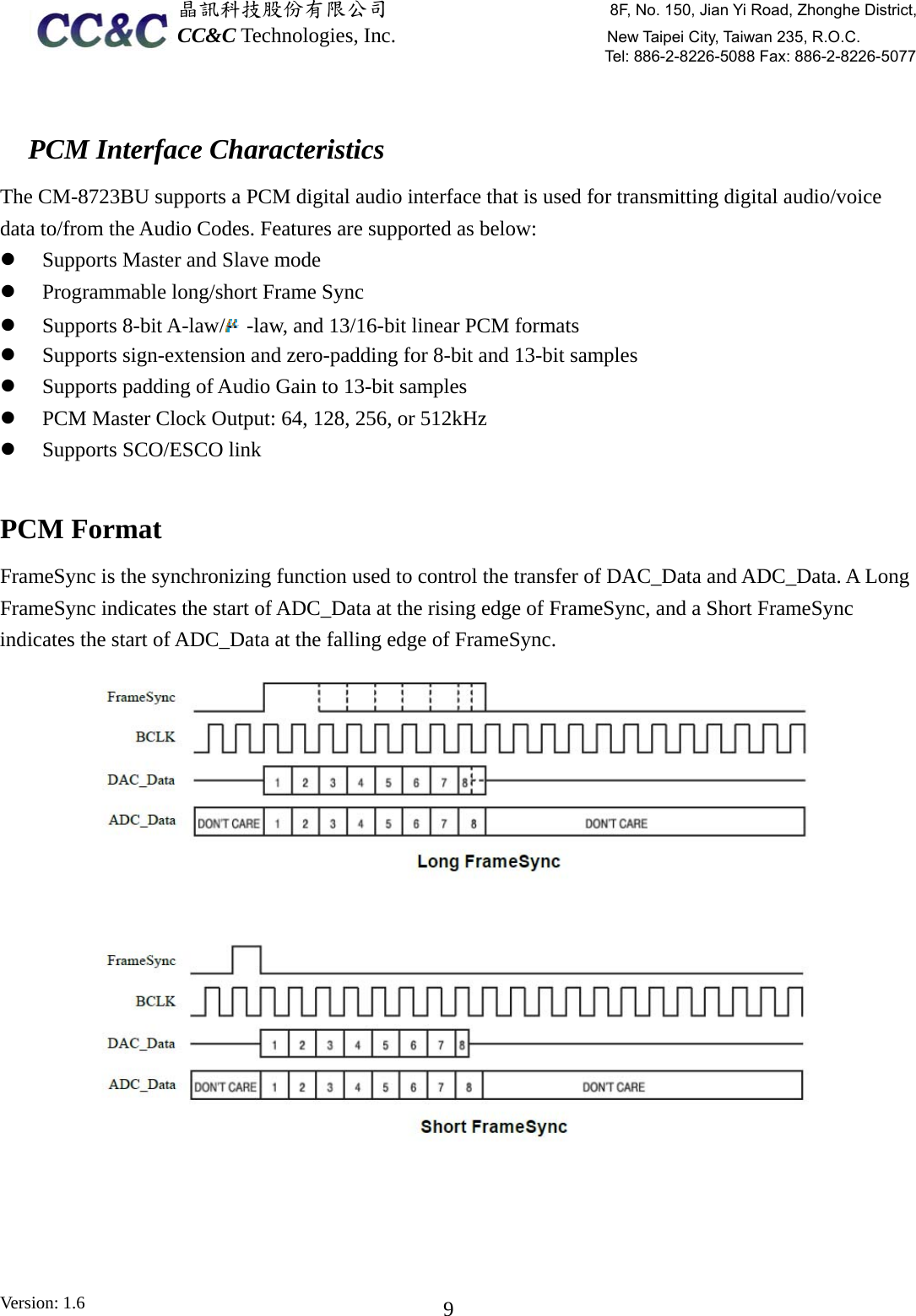
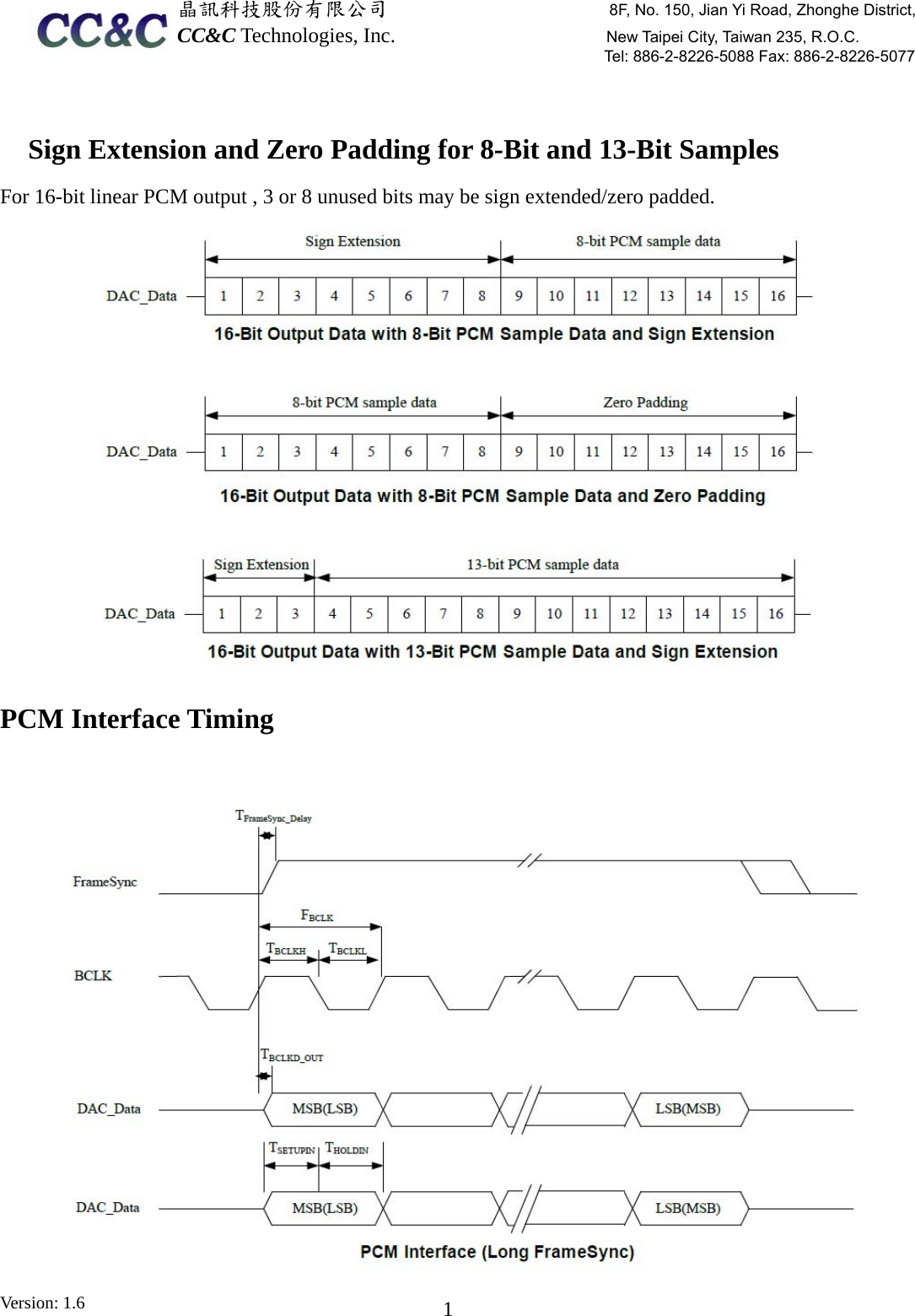
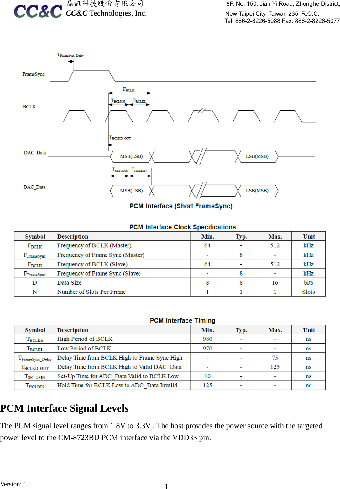
LM Technologies 811-04XX LM811 Wi-Fi & BT SMT Module User Manual Product Specifications

LM Technologies Ltd. LM811 Wi-Fi & BT SMT Module Product Specifications

User Manual

 晶訊科技股份有限公司                     8F, No. 150, Jian Yi Road, Zhonghe District,CC&C Technologies, Inc.                    New Taipei City, Taiwan 235, R.O.C. Tel: 886-2-8226-5088 Fax: 886-2-8226-5077 Version: 1.6    1        Product Specifications    LM811-045x11n+ BT WiFi module            Version: 1.6  Manufacturer CC&C Technologies, Inc.
 晶訊科技股份有限公司                     8F, No. 150, Jian Yi Road, Zhonghe District,CC&C Technologies, Inc.                    New Taipei City, Taiwan 235, R.O.C. Tel: 886-2-8226-5088 Fax: 886-2-8226-5077 Version: 1.6    2Revision History Version  Issue date  Reason for revision Preliminary  Aug. 1, 2014  Preliminary release 1.1  Aug. 18, 2014  Modify for Pin-out of module, dimension figure, and added factory options 1.2  Sep. 26, 2014  Add DC power input, power consumption item and operating temperature data 1.3  Jan. 12, 2015  Modify factory optional explanation 1.4  Mar. 3, 2015  Modify PCB pin out and add chip antenna optional 1.5  June 09, 2015  Modify dimension figure (Distance between Pin13 to PCB left) 1.6  Oct. 13, 2015  Add Interface Specification, Modify Pin outs define
 晶訊科技股份有限公司                     8F, No. 150, Jian Yi Road, Zhonghe District,CC&C Technologies, Inc.                    New Taipei City, Taiwan 235, R.O.C. Tel: 886-2-8226-5088 Fax: 886-2-8226-5077 Version: 1.6    3Overview LM811-045X  is a WLAN 11n and Bluetooth combo module, provides a single USB interface to host, which fully supports the features and functional compliance of IEEE 802.11b/g/n standards, Bluetooth v2.1, v3.0 and v4.0 standards. It supports up to 150Mbps WLAN network connections and Bluetooth protocol stack (LM, LL and LE), Bluetooth baseband and modem. It is designed to provide excellent performance with low power consumption and enhance the advantages of robust system and cost-effective. LM811-045X  provides a complete solution for a high throughput performance integrated wireless LAN and Bluetooth module, and is targeted at competitive superior performance, better power management applications.  Features  Operate at ISM frequency bands (2.4GHz)  IEEE standards support: IEEE 802.11b/ g/ n/ d/ e/ h/ i  Fully qualified Bluetooth 2.1 + EDR specification including both 2Mbps and 3Mbps modulation mode  Fully qualified Bluetooth 3.0  Fully qualified Bluetooth 4.0 Dual mode  Full speed Bluetooth operation with Pico net and Scatter net support  Enterprise level security which can apply WPA/WPA2 certification for WiFi  WiFi 1T1R, allow data rate supporting up to 150Mbps  Support sophisticated WiFi/BT coexistence mechanism to enhance collection performance  Support antenna diversity for WiFi and BT antenna selection  Support Bluetooth adaptive power management mechanism  Fully-featured software utility for easy configuration and management  RoHS compliance  Low Halogen compliance
 晶訊科技股份有限公司                     8F, No. 150, Jian Yi Road, Zhonghe District,CC&C Technologies, Inc.                    New Taipei City, Taiwan 235, R.O.C. Tel: 886-2-8226-5088 Fax: 886-2-8226-5077 Version: 1.6    4 General Specification Model Name  LM811-04  5xProduct Name   WLAN and Bluetooth combo module, USB interface Standards   IEEE 802.11b/g/n/d/e/h/i Bluetooth v2.1+EDR/ v3.0/ v3.0+HS/ v4.0 Data Transfer Rate  WLAN: 802.11b: 11, 5.5, 2, 1 Mbps 802.11g: 54, 48, 36, 24, 18, 12, 9, 6 Mbps 802.11n: MCS0 to 7 for HT20MHz, MCS0 to 7 for HT40MHz Bluetooth:  Basic rate: 1Mbps Enhanced data rate: 2, 3 Mbps High Speed: 6, 9, 12, 18, 24, 36, 48, 54 Mbps Modulation Method   WLAN:  802.11b: CCK, DQPSK, DBPSK 802.11g: 64QAM, 16QAM, QPSK, BPSK 802.11n: 64QAM, 16QAM, QPSK, BPSK Bluetooth: 8DPSK, π/4 DQPSK, GFSKFSK Operating Channel WLAN 2.4GHz:     11: (Ch. 1-11) – United States     13: (Ch. 1-13) – Europe     14: (Ch. 1-14) – Japan BT 2.4GHz:     Ch. 0 to 78 Frequency Range    2.4GHz ISM band (2.400GHz to 2.4835 GHz) Spread Spectrum WLAN IEEE 802.11b: DSSS (Direct Sequence Spread Spectrum) WLAN IEEE 802.11g/n: OFDM (Orthogonal Frequency Division Multiplexing)Bluetooth: FHSS (Frequency Hopping Spread Spectrum) RF Output Power (tolerance ±2dBm) WLAN:  17dBm – 802.11b@11Mbps 15dBm – 802.11g@6Mbps 14dBm – 802.11g@54Mbps 13dBm – 802.11n@MCS0_HT20 13dBm – 802.11n@MCS7_HT20 13dBm – 802.11n@MCS0_HT40 13dBm – 802.11n@MCS7_HT40 Bluetooth: Max + 8dBm Network architecture WLAN:  Ad hoc mode (Peer-to-Peer) Infrastructure mode Software AP WiFi Direct BT:    Pico Net   Scatter Net Receiver Sensitivity   WLAN:  -82dBm – 802.11b@11Mbps -71dBm – 802.11g@54MBps -67dBm – 802.11n@MCS7_HT20 -64dBm - 802.11n@MCS7_HT40 Bluetooth:  -89dBm@1Mbps
 晶訊科技股份有限公司                     8F, No. 150, Jian Yi Road, Zhonghe District,CC&C Technologies, Inc.                    New Taipei City, Taiwan 235, R.O.C. Tel: 886-2-8226-5088 Fax: 886-2-8226-5077 Version: 1.6    5-90dBm@2Mbps -83dBm@3Mbps Operation Range    WLAN: Up to 180 meters in open space Bluetooth: Great than 10 meters in open space OS Support  Windows XP/ Linux/ Android Security  WLAN: WPA, WPA-PSK, WPA2, WPA2-PSK, WEP 64bit & 128bit, IEEE 802.11x, IEEE 802.11i BT: Simple Paring Bus interface    USB 2.0 Operating Temperature    0 – 60° C ambient temperature 0 to 95 % (non-condensing) Storage Temperature    -20 ~ 70°C ambient temperature 0 to 95 % (non-condensing) Dimension   25 x 12 x 2 mm (LxWxH)          Factory options 1. DC power input 3.3V or 5V input and DC range as below table     Module Minimum Typical Maximum Unit DC 5V module 4.75  5  5.25  V DC 3.3V module  3.135 3.3  3.465  V  2. RF out can select below: RF connector (type-1), RF output on half-hole pin (type-2), RF out by chip antenna (type-3) RF type-1  RF type-2  RF type-3
 晶訊科技股份有限公司                     8F, No. 150, Jian Yi Road, Zhonghe District,CC&C Technologies, Inc.                    New Taipei City, Taiwan 235, R.O.C. Tel: 886-2-8226-5088 Fax: 886-2-8226-5077 Version: 1.6    6Power Consumption DC power for 5V Performance  Description TYP UNITS Off 10 uA Unassociated idle  40  mA Associated idle for 2.4GHz band  70  mA Data transfer for 2.4GHz  103  mA PS. Data transfer test using the Linux driver: Linux_v4.3.6_11841.20140714   DC power for 3.3V Performance  Description TYP UNITS Off 16 uA Unassociated idle  90  mA Associated idle for 2.4GHz band  141  mA Data transfer for 2.4GHz  168  mA PS. Data transfer test using the Linux driver: Linux_v4.3.6_11841.20140714
 晶訊科技股份有限公司                     8F, No. 150, Jian Yi Road, Zhonghe District,CC&C Technologies, Inc.                    New Taipei City, Taiwan 235, R.O.C. Tel: 886-2-8226-5088 Fax: 886-2-8226-5077 Version: 1.6    7Pin outs define:  Pin  Signal  Input /Output  Description 1 CHIP_WAKE_HOST  Output  Signal from module to wake up host,refer driver source code for details. 2 GND  Power  Ground 3  USB D+  I/O  USB D+ signal 4  USB D-  I/O  USB D- signal 5 VCC  Power  DC 3.3V 6 HOST_WAKE_CHIP  Input  Signal from host to wake up module,refer driver source code for details. 7 GND  Power  Ground 8  ANT  RF  WLAN/BT RF port (if don’t using IPEX connector) 9 GND  Power  Ground 10 BT_PCM_IN  Input  PCM data Input. This pin is also shared with GPIO0 and 3DG_SEL_A. 11 BT_PCM_OUT  Output  PCM data Output. This pin is also shared with GPIO1 and 3DG_SYNC_A. 12 BT_PCM_SYNK  I/O  PCM frame Synchronization. This pin is also shared with GPIO2. 13  BT_PCM_CLK  I/O  PCM Clock. This pin is also shared with GPIO3. 14  EXT_XIN  -  NC_ Keep to floating
 晶訊科技股份有限公司                     8F, No. 150, Jian Yi Road, Zhonghe District,CC&C Technologies, Inc.                    New Taipei City, Taiwan 235, R.O.C. Tel: 886-2-8226-5088 Fax: 886-2-8226-5077 Version: 1.6    8 Interface Timing Specification   USB Bus during Power On Sequence  The power on flow description: After main 3.3V ramp up, the internal power on reset is released by power ready detection circuit and the power management unit will be enabled. The power management unit enables the internal regulator and clock circuits. The power management unit also enables the USB circuits. USB analog circuits attach resisters to indicate the insertion of the USB device.
 晶訊科技股份有限公司                     8F, No. 150, Jian Yi Road, Zhonghe District,CC&C Technologies, Inc.                    New Taipei City, Taiwan 235, R.O.C. Tel: 886-2-8226-5088 Fax: 886-2-8226-5077 Version: 1.6    9 PCM Interface Characteristics The CM-8723BU supports a PCM digital audio interface that is used for transmitting digital audio/voice data to/from the Audio Codes. Features are supported as below: z Supports Master and Slave mode z Programmable long/short Frame Sync z Supports 8-bit A-law/ -law, and 13/16-bit linear PCM formats z Supports sign-extension and zero-padding for 8-bit and 13-bit samples z Supports padding of Audio Gain to 13-bit samples z PCM Master Clock Output: 64, 128, 256, or 512kHz z Supports SCO/ESCO link  PCM Format FrameSync is the synchronizing function used to control the transfer of DAC_Data and ADC_Data. A Long FrameSync indicates the start of ADC_Data at the rising edge of FrameSync, and a Short FrameSync indicates the start of ADC_Data at the falling edge of FrameSync.
 晶訊科技股份有限公司                     8F, No. 150, Jian Yi Road, Zhonghe District,CC&C Technologies, Inc.                    New Taipei City, Taiwan 235, R.O.C. Tel: 886-2-8226-5088 Fax: 886-2-8226-5077 Version: 1.6    1 Sign Extension and Zero Padding for 8-Bit and 13-Bit Samples For 16-bit linear PCM output , 3 or 8 unused bits may be sign extended/zero padded.  PCM Interface Timing
 晶訊科技股份有限公司                     8F, No. 150, Jian Yi Road, Zhonghe District,CC&C Technologies, Inc.                    New Taipei City, Taiwan 235, R.O.C. Tel: 886-2-8226-5088 Fax: 886-2-8226-5077 Version: 1.6    1   PCM Interface Signal Levels The PCM signal level ranges from 1.8V to 3.3V . The host provides the power source with the targeted power level to the CM-8723BU PCM interface via the VDD33 pin.
 晶訊科技股份有限公司                     8F, No. 150, Jian Yi Road, Zhonghe District,CC&C Technologies, Inc.                    New Taipei City, Taiwan 235, R.O.C. Tel: 886-2-8226-5088 Fax: 886-2-8226-5077 Version: 1.6    1  The CM-8723BU module WiFi/BT both single path S0 connection to ANT, and IPEX connector S1 path set to NC.  RF connector dimensions (unit: mm)
 晶訊科技股份有限公司                     8F, No. 150, Jian Yi Road, Zhonghe District,CC&C Technologies, Inc.                    New Taipei City, Taiwan 235, R.O.C. Tel: 886-2-8226-5088 Fax: 886-2-8226-5077 Version: 1.6    1 Dimension
 晶訊科技股份有限公司                     8F, No. 150, Jian Yi Road, Zhonghe District,CC&C Technologies, Inc.                    New Taipei City, Taiwan 235, R.O.C. Tel: 886-2-8226-5088 Fax: 886-2-8226-5077 Version: 1.6    1 Subject to change without notice PCB Layout footprint 1. The recommended layout pads for CM-8723BU module are shown below. (Module top view)
 晶訊科技股份有限公司                     8F, No. 150, Jian Yi Road, Zhonghe District,CC&C Technologies, Inc.                    New Taipei City, Taiwan 235, R.O.C. Tel: 886-2-8226-5088 Fax: 886-2-8226-5077 Version: 1.6    1 All dimensions are in millimeters. Tolerance: +- 0.05mm Reference Temperature Reflow Chart
 晶訊科技股份有限公司                     8F, No. 150, Jian Yi Road, Zhonghe District,CC&C Technologies, Inc.                    New Taipei City, Taiwan 235, R.O.C. Tel: 886-2-8226-5088 Fax: 886-2-8226-5077 Version: 1.6    1    This module is surface mount device; please refer below conditions for drying before solder reflow processes. (extracted from IPC/JEDEC J-STD-033B.1)   Bake @ 125 oC  Bake @ 90 oC  Bake @ 40 oC Exceeding  floor Life By > 72h Exceeding  floor Life By ≤ 72h Exceeding floor Life By > 72h Exceeding floor Life By ≤ 72h Exceeding  floor Life By > 72h Exceeding floor Life By ≤ 72h  9 hours   7 hours  33 hours  23 hours  13 days  9 days
 FCC Warning  This device complies with Part 15 of the FCC Rules. Operation is subject to the following two conditions: (1) This  device m ay not c ause harmful int erference, a nd ( 2) th is device m ust acc ept any  interference rec eived, including interference that may cause undesired operation.  NOTE 1: T his eq uipment has been tested and fo und to  c omply with  t he limits for a  Class B d igital d evice, pursuant to part 15 of the FCC Rules. These limits are designed to provide reasonable protection against harmful interference in a  resi dential installation. This equipment generates, uses and can radiate radio freque ncy energy and, if  not i nstalled and  used i n accordance wit h t he instr uctions, may cause  harmful in terference t o ra dio communications. However, there is no guarantee that interference will not occur in a particular installation. If this equipment does cause harmful interference to radio or television reception, which can be determined by turning the equipment off and on, the user is encouraged to try to correct the interference by one or more of the following measures: - Reorient or relocate the receiving antenna. - Increase the separation between the equipment and receiver. -Connect the equipment into an outlet on a circuit different from that to which the receiver is connected. -Consult the dealer or an experienced radio/TV technician for help.  NOTE 2 : Any ch anges or m odifications t o th is un it no t ex pressly ap proved by t he party resp onsible for compliance could void the user's authority to operate the equipment.  FCC Radiation Exposure Statement:  This equipment complies with FCC radiation exposure limits set forth for an uncontrolled environment. End users must follow the specific operating instructions for satisfying RF exposure compliance.  Note 1: Compliance of this device in all final host configurations is the responsibility of the Grantee.     OEM integrators are responsible to satisfy RF exposure requirements. SAR evaluation is valid for portable, mobile and fixed applications.    The highest reported SAR value for body condition is 0.664W/kg respectively. This device was tested simulationtypical 5mm separation distance from the body.   Note 2: Any modifications made to the module will void the Grant of Certification, this module is limited to OEM installation only and must not be sold to end-users, end-user has no manual instructions to remove or install the device, only software or operating procedure shall be placed in the end-user operating manual of final products.  Note 3: The device must not transmit simultaneously with any other antenna or transmitter.  Note 4: To ensure compliance with all non-transmitter functions the host manufacturer is responsible for ensuring compliance with the module(s) installed and fully operational. For example, if a host was previously authorized as an unintentional radiator under the Declaration of Conformity procedure without a transmitter certified module
and a module is added, the host manufacturer is responsible for ensuring that the after the module is installed and operational the host continues to be compliant with the Part 15B unintentional radiator requirements. Since this may depend on the details of how the module is integrated with the host, LM Technologies Ltd. shall provide guidance to the host manufacturer for compliance with the Part 15B requirements.  Note 5: FCC ID label on the final system must be labeled with “Contains FCC ID: VVX811-04XX” or “Contains transmitter module FCC ID: VVX811-04XX”.  The transmitter module m ust b e installed an d used in strict ac cordance wit h t he manufacturer's ins tructions as described in the user documentation that comes with the host product. LM Technologies Ltd. is responsible for the compliance of the module in all final hosts.

Navigation menu