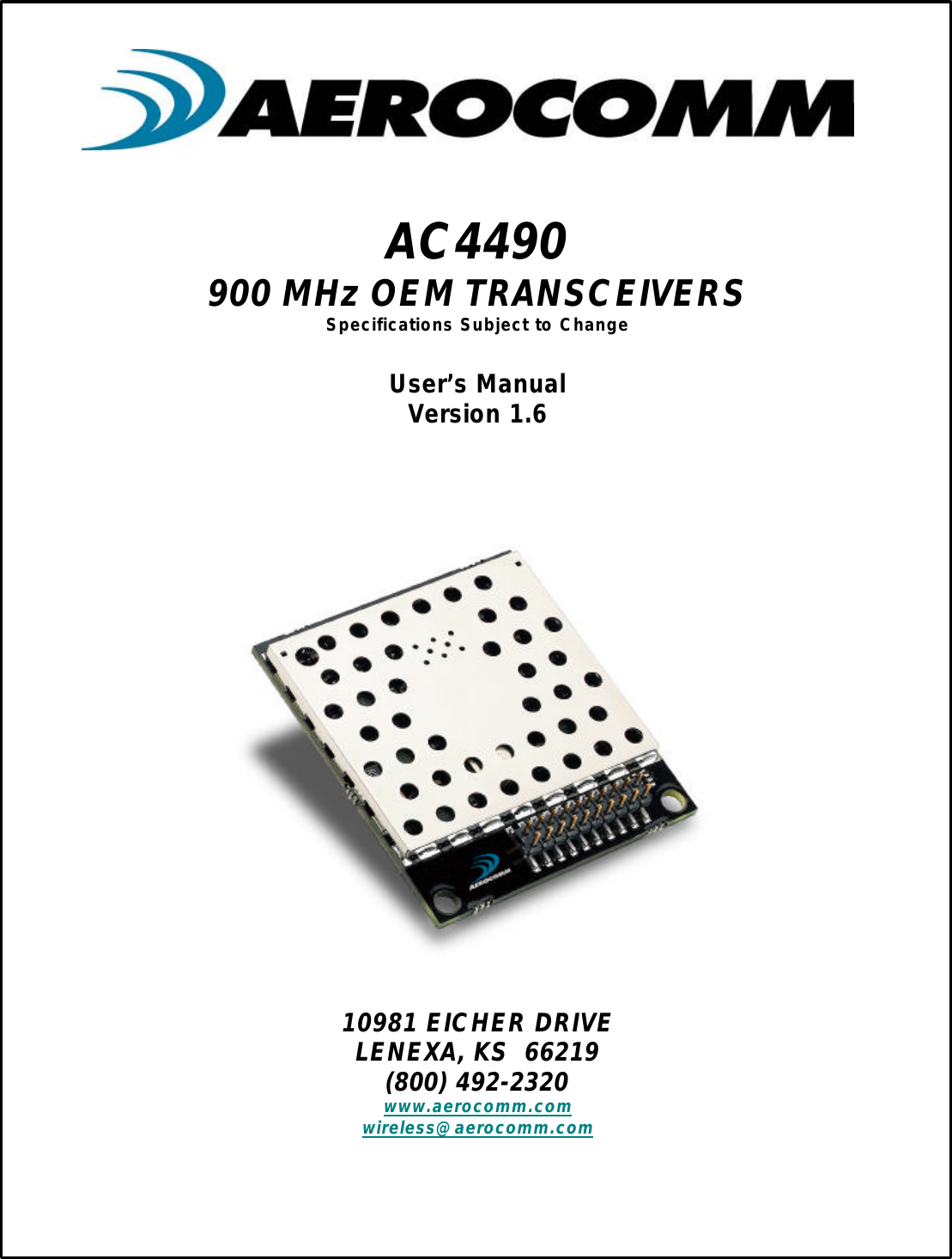
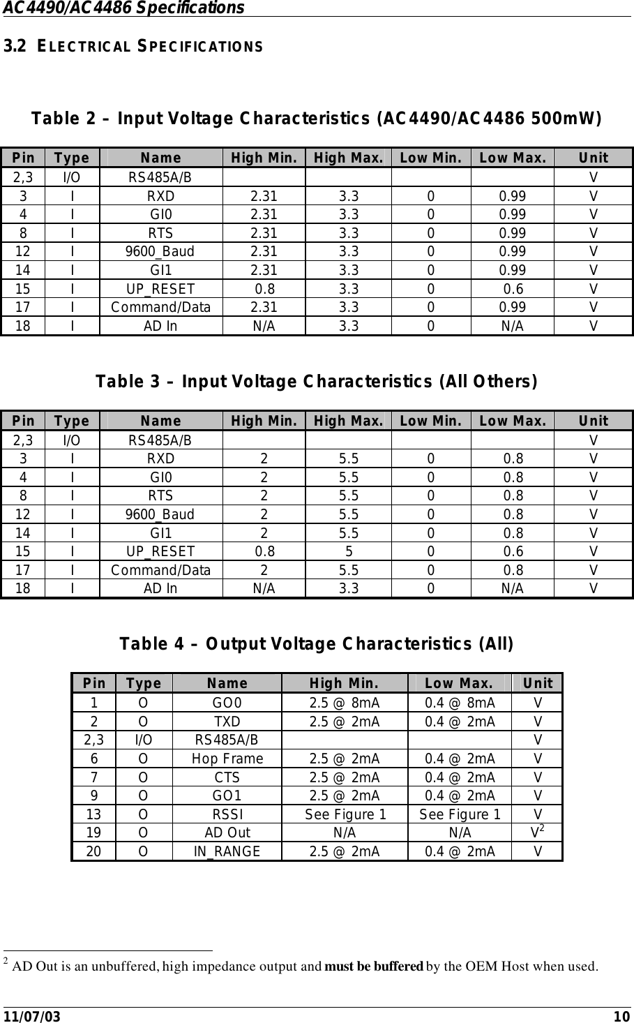
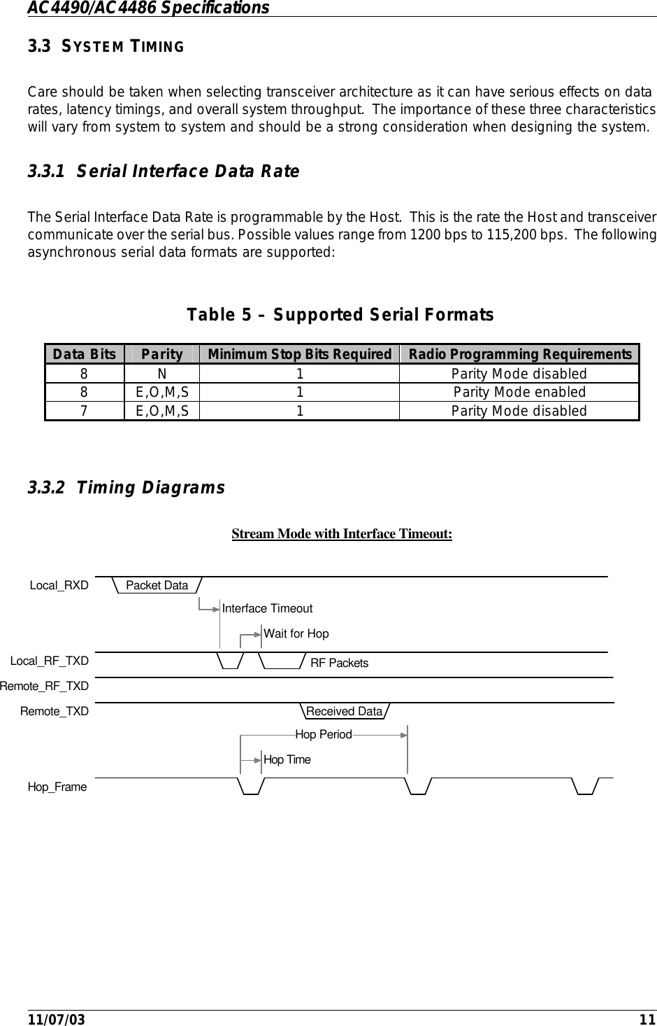
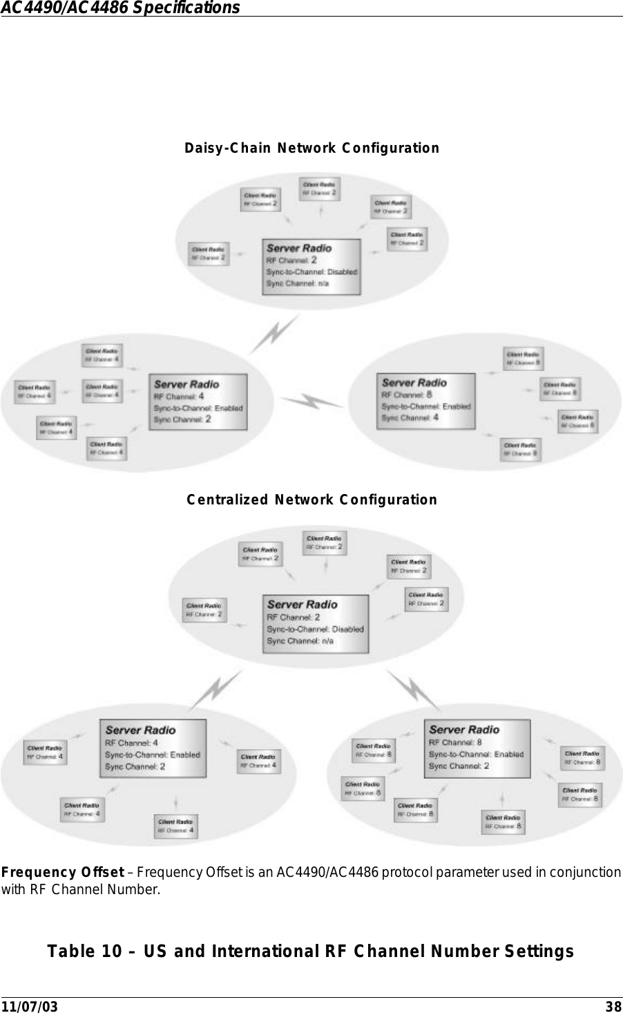
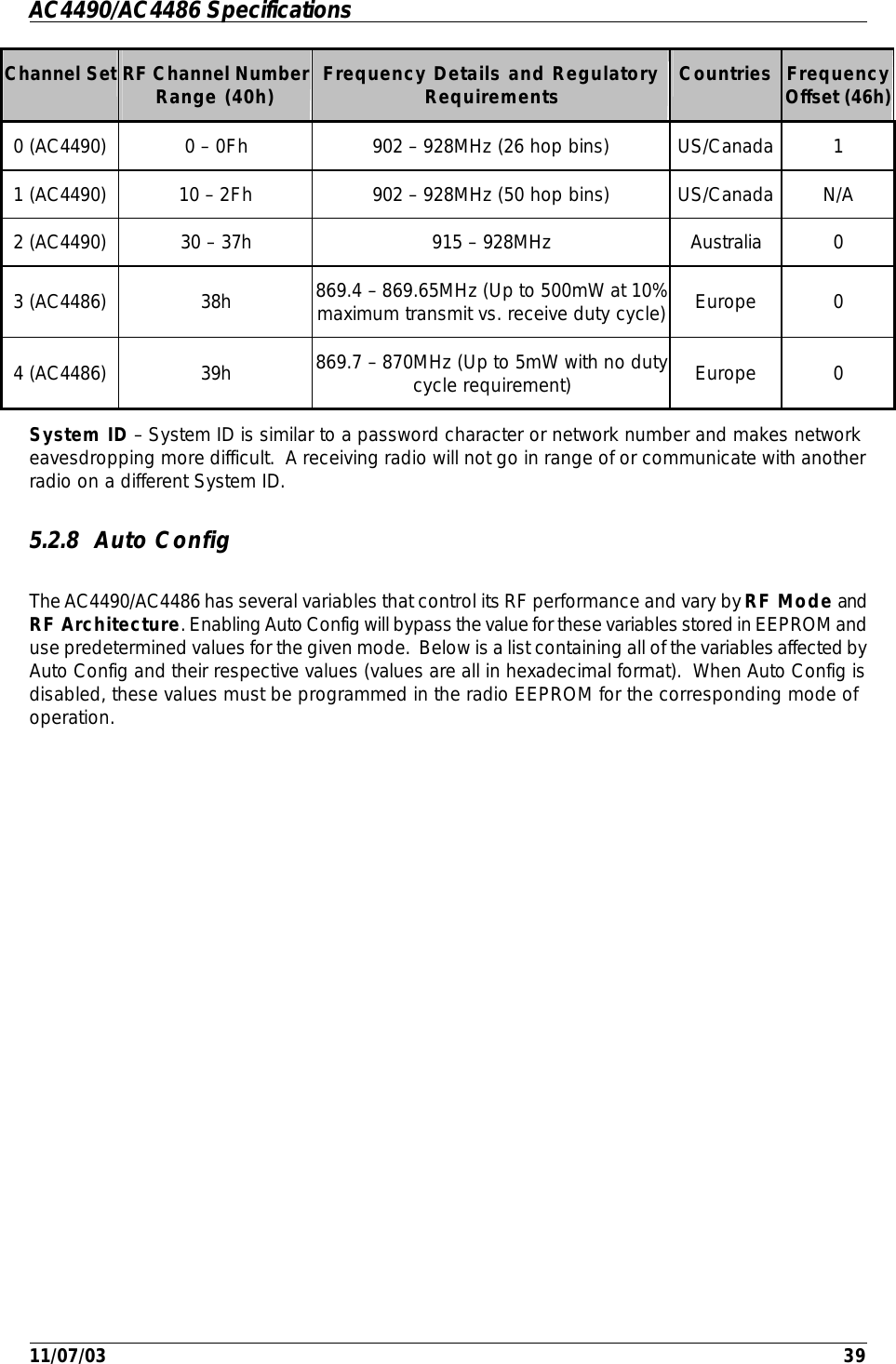
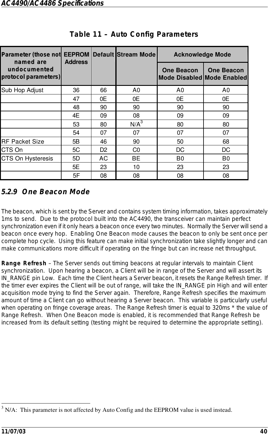
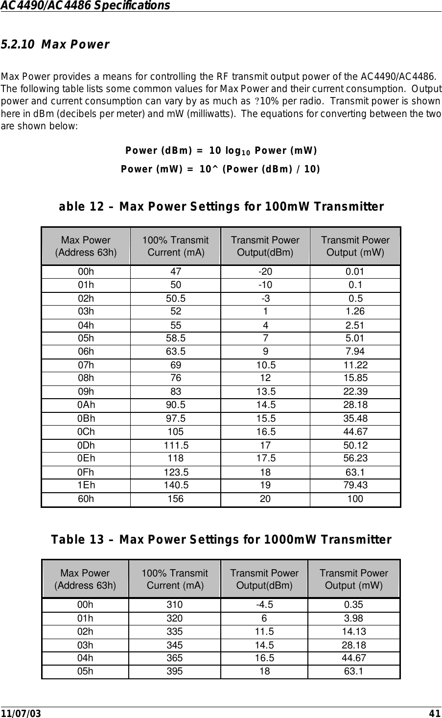
Laird Connectivity AC4490 RF Transceiver Module User Manual AC4490 AC4486 User s Manual v1 6
AeroComm Corporation RF Transceiver Module AC4490 AC4486 User s Manual v1 6
UserManual.wiki
>
Laird Connectivity
>
AC4490 User Manual
>
Users Manual Part 1
Contents
1.
Users Manual Part 1
2.
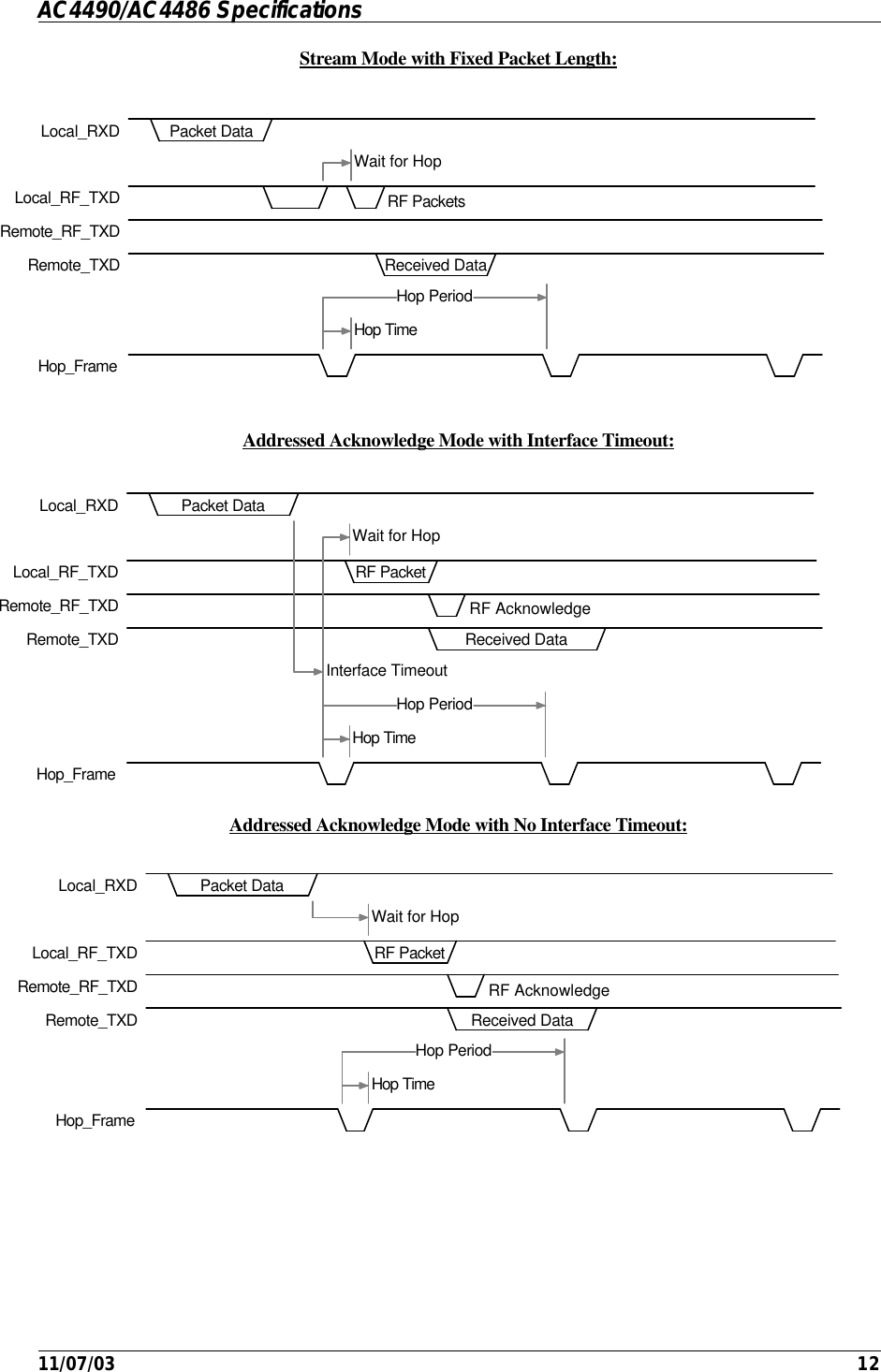
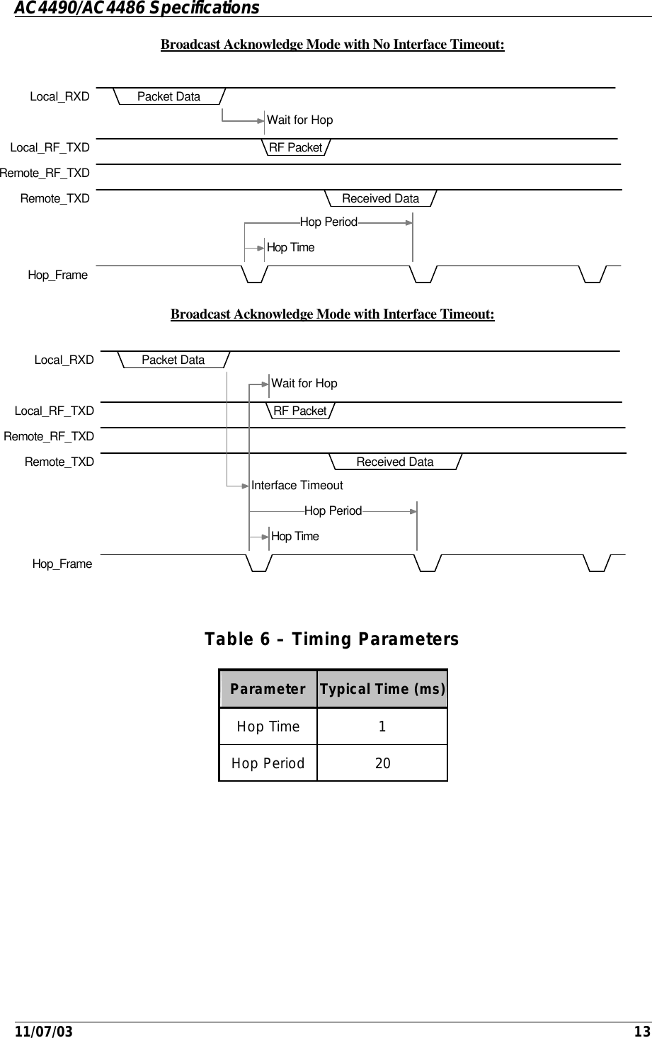
Users Manual Part 2
3.
User Manual final
4.
User Manual-1
5.
User Manual-2
6.
Users Manual-1
7.
Users Manual-2
Users Manual Part 1
Navigation menu
Upload a User Manual
Namespaces
Wiki Guide
HTML
PDF
Info
Views
User Manual
Discussion / Help
Navigation