Laird Connectivity AC4490 RF Transceiver Module User Manual AC4490 AC4486 User s Manual v1 6
AeroComm Corporation RF Transceiver Module AC4490 AC4486 User s Manual v1 6
Contents
Users Manual Part 1
AC4490
900 MHz OEM TRANSCEIVERS
Specifications Subject to Change
User’s Manual
Version 1.6
10981 EICHER DRIVE
LENEXA, KS 66219
(800) 492-2320
www.aerocomm.com
wireless@aerocomm.com

11/07/03 2
DOCUMENT INFORMATION
Copyright
Information Copyright © 2003 AEROCOMM, Inc. All rights reserved.
The information contained in this manual and the accompanying
software programs are copyrighted and all rights are reserved by
AEROCOMM, Inc. AEROCOMM, Inc. reserves the right to make
periodic modifications of this product without obligation to notify
any person or entity of such revision. Copying, duplicating, selling, or otherwise
distributing any part of this product or accompanying documentation/software
without the prior consent of an authorized representative of AEROCOMM, Inc. is
strictly prohibited.
All brands and product names in this publication are registered
trademarks or trademarks of their respective holders.
This material is preliminary
Information furnished by AEROCOMM
in this specification is believed to be accurate. Devices sold
by AEROCOMM are covered by the warranty and patent indemnification provisi
ons appearing in its
Terms of Sale only. AEROCOMM makes no warranty, express, statutory, and implied or by
description, regarding the information set forth herein. AEROCOMM
reserves the right to change
specifications at any time and without notice.
AEROCOMM’s products are intended for use in normal commercial and industrial applications.
Applications requiring unusual environmental requirements such as military, medical life-
support
or life-sustaining equipment are specifically not recommended without ad
ditional testing for such
application.

11/07/03 3
DOCUMENT INFORMATION

11/07/03 4
TABLE OF CONTENTS
1. OVERVIEW ......................................................................................................................................................7
2. AC4490/AC4486 SPECIFICATIONS.........................................................................................................8
3. SPECIFICATIONS..........................................................................................................................................9
3.1 INTERFACE SIGNAL DEFINITIONS......................................................................................................................9
3.2 ELECTRICAL SPECIFICATIONS..........................................................................................................................10
3.3 SYSTEM TIMING..................................................................................................................................................11
3.3.1 Serial Interface Data Rate.....................................................................................................................11
3.3.2 Timing Diagrams.....................................................................................................................................11
3.3.3 Maximum Overall System Throughput................................................................................................14
4. CONFIGURING THE AC4490/AC4486.................................................................................................15
4.1 EEPROM PARAMETERS...................................................................................................................................15
4.2 EEPROM CONFIGURATION COMMANDS.......................................................................................................18
4.2.1 EEPROM Byte Read ...............................................................................................................................18
4.2.2 EEPROM Byte Write...............................................................................................................................18
4.2.3 EEPROM Exit Configuration Mode Command.................................................................................19
4.3 AC4490 AT COMMANDS..................................................................................................................................19
4.3.1 Enter AT Command Mode......................................................................................................................19
4.3.2 Exit AT Command Mode........................................................................................................................20
4.4 ON-THE-FLY CONTROL COMMAND REFERENCE (CC COMMAND MODE)................................................20
4.4.1 Status Request..........................................................................................................................................21
4.4.2 Change Channel without Forced Acquisition Sync...........................................................................21
4.4.3 Change Channel with Forced Acquisition Sync.................................................................................21
4.4.4 Server/Client Command.........................................................................................................................22
4.4.5 Sync to Channel Command....................................................................................................................22
4.4.6 Sleep Walk Power-Down Command....................................................................................................23
4.4.7 Sleep Walk Power-Down Wake-Up Command ..................................................................................23
4.4.8 Broadcast Mode.......................................................................................................................................23
4.4.9 Read Static Bank #1 Byte.......................................................................................................................24
4.4.10 Write Static Bank #1 Byte......................................................................................................................24
4.4.11 Read Static Bank #2 Byte.......................................................................................................................24
4.4.12 Write Static Bank #2 Byte......................................................................................................................26
4.4.13 Write Destination Address.....................................................................................................................26
4.4.14 Read Destination Address......................................................................................................................26
4.4.15 Read Digital Inputs.................................................................................................................................27
4.4.16 Read ADC .................................................................................................................................................27
4.4.17 Report Last Valid RSSI...........................................................................................................................28
4.4.18 Write Digital Outputs..............................................................................................................................28
4.4.19 Write DAC ................................................................................................................................................29
4.4.20 Set Max Power.........................................................................................................................................29
4.4.21 Transmit Buffer Empty............................................................................................................................30
4.4.22 Disable Sync to Channel ........................................................................................................................30
4.4.23 Deep Sleep Mode.....................................................................................................................................30
4.4.24 Reset Command .......................................................................................................................................30
5. THEORY OF OPERATION.......................................................................................................................31
5.1 HARDWARE INTERFACE.....................................................................................................................................31
5.1.1 GIn (Generic Inputs 0 and 1) (pins 4 and 14 respectively) and GOn (Generic Outputs 0 and 1)
(pins 1 and 9 respectively).......................................................................................................................................31
5.1.2 TXD (Transmit Data) and RXD (Receive Data) (pins 2 and 3 respectively)................................31

11/07/03 5
5.1.3 Hop Frame (pin 6)...................................................................................................................................31
5.1.4 CTS Handshaking (pin 7).......................................................................................................................32
5.1.5 RTS Handshaking (pin 8).......................................................................................................................32
5.1.6 9600 Baud (pin 12)..................................................................................................................................32
5.1.7 RSSI (pin 13)............................................................................................................................................32
5.1.8 UP_Reset (pin 15) ...................................................................................................................................33
5.1.9 Command/Data (pin 17).........................................................................................................................33
5.1.10 AD In and DA Out (pins 18 and 19 respectively) ..............................................................................34
5.1.11 In Range (pin 20).....................................................................................................................................34
5.2 SOFTWARE PARAMETERS..................................................................................................................................35
5.2.1 RF Architecture (Unicast/Broadcast)..................................................................................................35
5.2.2 RF Mode....................................................................................................................................................35
5.2.3 Sub Hop Adjust ........................................................................................................................................36
5.2.4 Duplex Mode............................................................................................................................................36
5.2.5 Interface Timeout/RF Packet Size........................................................................................................36
5.2.6 Serial Interface Baud Rate.....................................................................................................................37
5.2.7 Network Topology...................................................................................................................................37
5.2.8 Auto Config...............................................................................................................................................39
5.2.9 One Beacon Mode...................................................................................................................................40
5.2.10 Max Power................................................................................................................................................41
5.2.11 Interface Options.....................................................................................................................................42
6. DIMENSIONS.................................................................................................................................................44
7. ORDERING INFORMATION...................................................................................................................47
7.1 PRODUCT PART NUMBER TREE........................................................................................................................47
7.2 DEVELOPER KIT PART NUMBERS....................................................................................................................47
8. AGENCY COMPLIANCY INFORMATION........................................................................................48
8.1 AGENCY IDENTIFICATION NUMBERS...............................................................................................................48
8.2 APPROVED ANTENNA LIST ...............................................................................................................................48
8.3 FCC/INDUSTRY CANADA (IC) REQUIREMENTS FOR MODULAR APPROVAL............................................49
8.3.1 OEM Equipment Labeling Requirements............................................................................................49
8.3.2 Antenna Requirements............................................................................................................................50
8.3.3 Warnings Required in OEM Manuals..................................................................................................50
RF Exposure Warning for Portable Equipment (<2.5cm) .................................................................................50
RF Exposure Warning for Portable Equipment (>2.5cm) .................................................................................50
RF Exposure for Warning for Mobile Equipment................................................................................................50
8.4 EUROPE/ETSI REQUIREMENTS FOR MODULAR APPROVAL........................................................................50
Figures
Figure 1 – RSSI Voltage vs. Received Signal Strength.......................................................................................... 33
Figure 2 - AC4490/AC4486 (with MMCX Connector) Mechanical.................................................................... 44
Figure 3 - AC4490 (with Integral GigaAnt Antenna) Mechanical........................................................................ 45
Figure 4 - AC4490/AC4486 (with Integral Splatch Antenna) Mechanical......................................................... 45
Tables
Table 1 – Pin Definitions................................................................................................................................................ 9
Table 2 – Input Voltage Characteristics (AC4490/AC4486 500mW).................................................................. 10
Table 3 – Input Voltage Characteristics (All Others).............................................................................................. 10
Table 4 – Output Voltage Characteristics (All) ........................................................................................................ 10
Table 5 – Supported Serial Formats ........................................................................................................................... 11
Table 6 – Timing Parameters ....................................................................................................................................... 13
Table 7 – Maximum Overall System Throughputs.................................................................................................. 14

11/07/03 6
Table 8 – EEPROM Parameters .................................................................................................................................. 15
Table 9 – Baud Rate/Interface Timeout..................................................................................................................... 37
Table 10 – US and International RF Channel Number Settings............................................................................ 38
Table 11 – Auto Config Parameters ........................................................................................................................... 40
Table 12 – Max Power Settings for 5mW Transmitter ......................................... Error! Bookmark not defined.
Table 13 – Max Power Settings for 100mW Transmitter....................................................................................... 41
Table 14 – Max Power Settings for 500mW Transmitter....................................................................................... 41
Table 15 – Transceiver Interface to DCE (Server Radio)....................................................................................... 43
Table 16 – Transceiver Interface to DTE (Client Radio)........................................................................................ 43
Table 17 – Agency Identification Numbers .............................................................................................................. 48
Table 18 – AC4490/AC4486 Approved Antenna List............................................................................................ 48

AC4490/AC4486 Specifications
11/07/03 7
AC4490/AC4486 Features
?? Available in either 3.3V or 5V TTL level serial interface for fast integration
?? Drop-in replacement for AC4424 2.4GHz product family
?? Two generic input and output digital lines and integrated DAC/ADC functions
?? Frequency Hopping Spread Spectrum for security and interference rejection
?? Cost Efficient for high volume applications
?? Very low power consumption for battery powered implementations
?? Small size for portable and enclosed applications
?? Very Low latency and high throughput
?? All modules are qualified for Industrial temperatures (-40°C to 80°C)
1. Overview
The AC4490/AC4486 and AC4486 are members of AeroComm’s ConnexRF OEM transceiver family.
The AC4490 is designed for integration into OEM systems operating under FCC part 15.247
regulations for the 900 MHz ISM band. The AC4486 is designed for integration into OEM systems
operating under European ETSI regulations for the 868 MHz band.
The AC4490 is a cost-effective, high performance, frequency hopping spread spectrum transceiver. It
provides an asynchronous TTL/RS-485 level serial interface for OEM Host communications.
Communications include both system and configuration data. The Host supplies system data for
transmission to other Host(s). Configuration data is stored in an on-board EEPROM. All frequency
hopping, synchronization, and RF system data transmission/reception is performed by the transceiver.
These transceivers can be used as a direct serial cable replacement – requiring no special Host
software for operation. They also feature a number of On-the-Fly Control Commands providing the
OEM with a very versatile interface for any network.
AC4490/AC4486 transceivers operate in a Point-to-Point or Point-to-Multipoint, Client-Server or Peer-to-
Peer architecture. One transceiver is configured as a Server and there can be one or many Clients. To
establish synchronization between transceivers, the Server emits a beacon. Upon detecting a beacon,
a Client transceiver informs its Host and a RF link is established.
This document contains information about the hardware and software interface between an
AeroComm AC4490/AC4486 transceiver and an OEM Host. Information includes the theory of
operation, specifications, interface definition, configuration information and mechanical drawing.
The OEM is responsible for ensuring the final product meets all FCC and/or appropriate regulatory
agency requirements listed herein before selling any product.

AC4490/AC4486 Specifications
11/07/03 8
2. AC4490/AC4486 Specifications
GENERAL
Interface 20 pin mini-connector
Serial Interface Data Rate PC baud rates from 1200 bps to 115,200 bps
Power Consumption (typical) Duty Cycle (TX=Transmit; RX=Receive)
10%TX 50%TX 100%TX 100%RX Pwr-DownDeep Sleep
AC4490-200:43mA 95mA 106mA 30mA 19mA 6mA
AC4490-1000:126mA 508mA 985mA 30mA 19mA 6mA
Channels 5 Channel Sets comprising 58 total channels
Security One byte System ID.
Interface Buffer Size Input/Output: 256 bytes each
RADIO
Frequency Band US/Canada: 902 – 928 MHz
Australia: 915 – 928 MHz
RF Data Rate 76.8kbps
Radio Type AC4490: Frequency Hopping Spread Spectrum
Output Power (conducted, no
antenna) AC4490-200: 100mW typical
AC4490-1000: 1000mW
Effective Isotropic Radiated Power
(EIRP with 3dBi gain antenna) AC4490-200: 200mW typical
AC4490-1000: 1000mW
Supply Voltage AC4490-200: 3.3 or 3.45 - 6V ±2%, ±50mV ripple
AC4490-1000: 3.3 ±2%, ±50mV ripple
Sensitivity -100dBm typical @ 76.8kbps
Range, Line of Site (based on 3dBi
gain antenna)
AC4490-200: 4 miles
AC4490-1000: 20 miles
ENVIRONMENTAL
Temperature (Operating)
-40?C to 80?C
Temperature (Storage) -50?C to +85?C
Humidity (non-condensing) 10% to 90% PHYSICAL
Dimensions 1.65” x 1.9” x 0.20”
Antenna AC4490-200: MMCX Connector or integral antenna
AC4490-1000: MMCX Connector
Weight Less than 0.75 ounce

AC4490/AC4486 Specifications
11/07/03 9
3. Specifications
3.1 INTERFACE SIGNAL DEFINITIONS
The AC4490/AC4486 has a simple interface that allows OEM Host communications with the transceiver.
Table 1 – Pin Definitions, shows the connector pin numbers and associated functions. The I/O direction
is with respect to the transceiver. All outputs are 3.3VDC levels and inputs are 5VDC TTL (with the
exception of 500mW radios which are 3.3V inputs) with the exception of RSSI, AD In and DA Out, which
are all analog. All inputs are weakly pulled High and may be left floating during normal operation.
Table 1 – Pin Definitions
Pin Type
Signal Name Function
1 O GO0 Generic Output pin
O TXD Transmitted data out of the transceiver
2 I/O RS485 A (True)1 Noninverted RS-485 representation of serial data
I RXD Data input to the transceiver
3 I/O RS485 B (Invert)2 Mirror image of RS-485 A
4 I GI0 Generic Input pin
5 GND GND Signal Ground
6 O Hop Frame Pulses Low when the transceiver is hopping.
7 O CTS Clear to Send – Active Low when the transceiver is ready to accept data for transmission.
8 I RTS Request to Send – When enabled in EEPROM, the OEM Host can take this High when it
is not ready to accept data from the transceiver. NOTE: Keeping RTS High for too long
can cause data loss.
9 O GO1 Generic Output pin
10 PWR VCC 3.3 or 3.45 – 6V (depends on model) ± 2%, ± 50mV ripple
11 PWR VCC 3.3 or 3.45 – 6V (depends on model) ± 2%, ±50 mV ripple
12 I 9600_BAUD 9600_BAUD – When pulled logic Low before applying power or resetting the
transceiver’s serial interface is forced to a 9600, 8, N, 1 rate. To exit, transceiver must be
reset or power-cycled with 9600_Baud logic High.
13 O RSSI Received Signal Strength - An analog output giving an instantaneous indication of
received signal strength. Only valid while in Receive Mode.
14 I GI1 Generic Input pin
15 I UP_RESET RESET – Controlled by the AC4490/AC4486 for power-on reset if left unconnected. After
a Stable power-on reset, a logic High pulse will reset the transceiver.
16 GND GND Signal Ground
17 I Command/Data When logic Low, the transceiver interprets Host data as command data. When logic
High, the transceiver interprets Host data as transmit data.
18 I AD In 10 bit Analog Data Input
19 O DA Out 10 bit Analog Data Output
20 O IN_RANGE In Range – Active Low when a Client radio is in range of a Server on same Channel with the
same System ID. Always Low on a Server.
I = Input to the transceiver O = Output from the transceiver
1 When ordered with a RS-485 interface.

AC4490/AC4486 Specifications
11/07/03 10
3.2 ELECTRICAL SPECIFICATIONS
Table 2 – Input Voltage Characteristics (AC4490/AC4486 500mW)
Pin Type
Name High Min.
High Max.
Low Min.
Low Max.
Unit
2,3 I/O RS485A/B V
3 I RXD 2.31 3.3 0 0.99 V
4 I GI0 2.31 3.3 0 0.99 V
8 I RTS 2.31 3.3 0 0.99 V
12 I 9600_Baud 2.31 3.3 0 0.99 V
14 I GI1 2.31 3.3 0 0.99 V
15 I UP_RESET 0.8 3.3 0 0.6 V
17 I Command/Data 2.31 3.3 0 0.99 V
18 I AD In N/A 3.3 0 N/A V
Table 3 – Input Voltage Characteristics (All Others)
Pin Type
Name High Min.
High Max.
Low Min.
Low Max.
Unit
2,3 I/O RS485A/B V
3 I RXD 2 5.5 0 0.8 V
4 I GI0 2 5.5 0 0.8 V
8 I RTS 2 5.5 0 0.8 V
12 I 9600_Baud 2 5.5 0 0.8 V
14 I GI1 2 5.5 0 0.8 V
15 I UP_RESET 0.8 5 0 0.6 V
17 I Command/Data 2 5.5 0 0.8 V
18 I AD In N/A 3.3 0 N/A V
Table 4 – Output Voltage Characteristics (All)
Pin Type Name High Min. Low Max. Unit
1 O GO0 2.5 @ 8mA 0.4 @ 8mA V
2 O TXD 2.5 @ 2mA 0.4 @ 2mA V
2,3 I/O RS485A/B V
6 O Hop Frame 2.5 @ 2mA 0.4 @ 2mA V
7 O CTS 2.5 @ 2mA 0.4 @ 2mA V
9 O GO1 2.5 @ 2mA 0.4 @ 2mA V
13 O RSSI See Figure 1 See Figure 1 V
19 O AD Out N/A N/A V2
20 O IN_RANGE 2.5 @ 2mA 0.4 @ 2mA V
2 AD Out is an unbuffered, high impedance output and must be buffered by the OEM Host when used.
AC4490/AC4486 Specifications
11/07/03 11
3.3 SYSTEM TIMING
Care should be taken when selecting transceiver architecture as it can have serious effects on data
rates, latency timings, and overall system throughput. The importance of these three characteristics
will vary from system to system and should be a strong consideration when designing the system.
3.3.1 Serial Interface Data Rate
The Serial Interface Data Rate is programmable by the Host. This is the rate the Host and transceiver
communicate over the serial bus. Possible values range from 1200 bps to 115,200 bps. The following
asynchronous serial data formats are supported:
Table 5 – Supported Serial Formats
Data Bits
Parity Minimum Stop Bits Required
Radio Programming Requirements
8 N 1 Parity Mode disabled
8 E,O,M,S 1 Parity Mode enabled
7 E,O,M,S 1 Parity Mode disabled
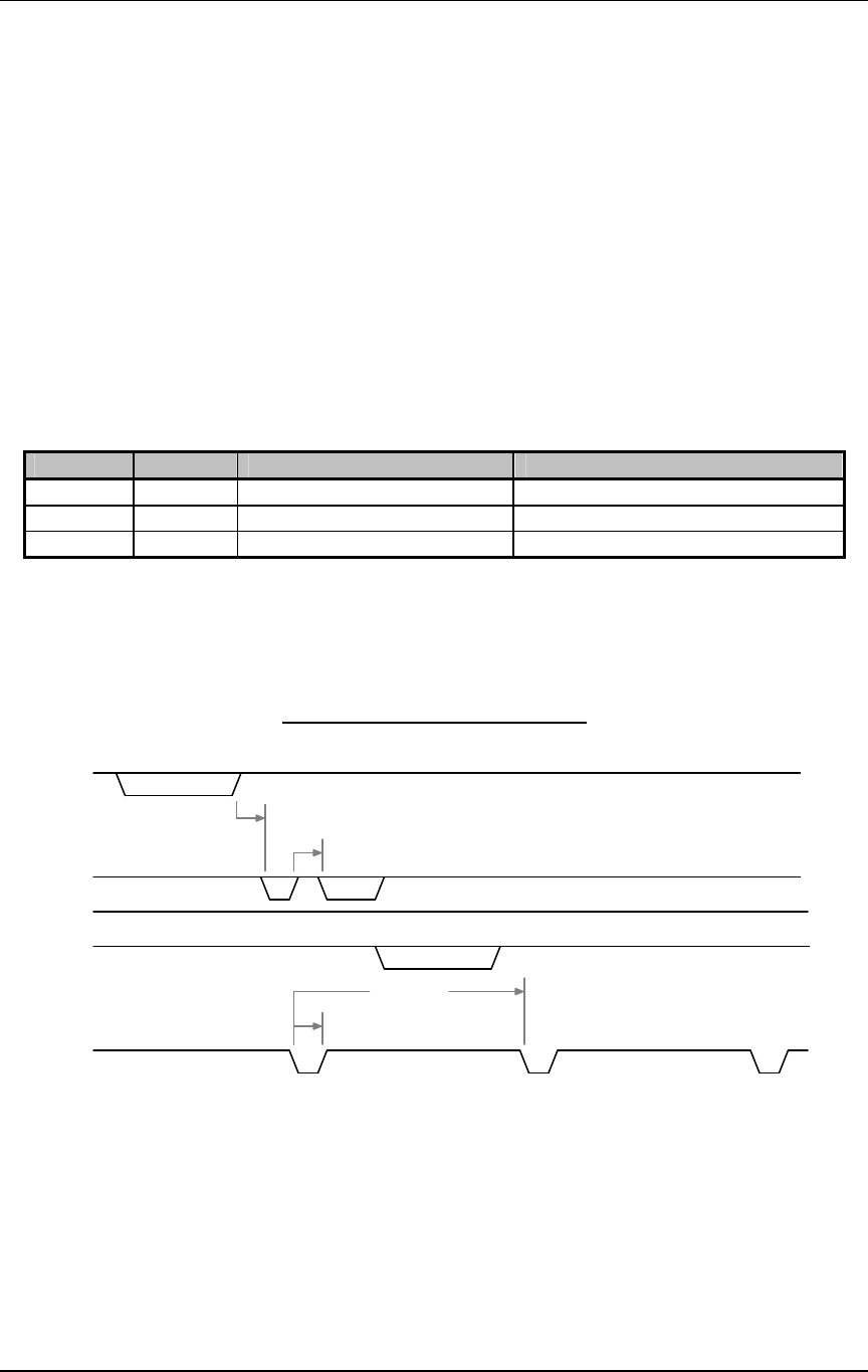
3.3.2 Timing Diagrams
Stream Mode with Interface Timeout:
Local_RXD
Local_RF_TXD
Remote_RF_TXD
Remote_TXD
Hop_Frame
Packet Data
Received Data
RF Packets
Hop Time
Wait for Hop
Interface Timeout
Hop Period

AC4490/AC4486 Specifications
11/07/03 12
Stream Mode with Fixed Packet Length:
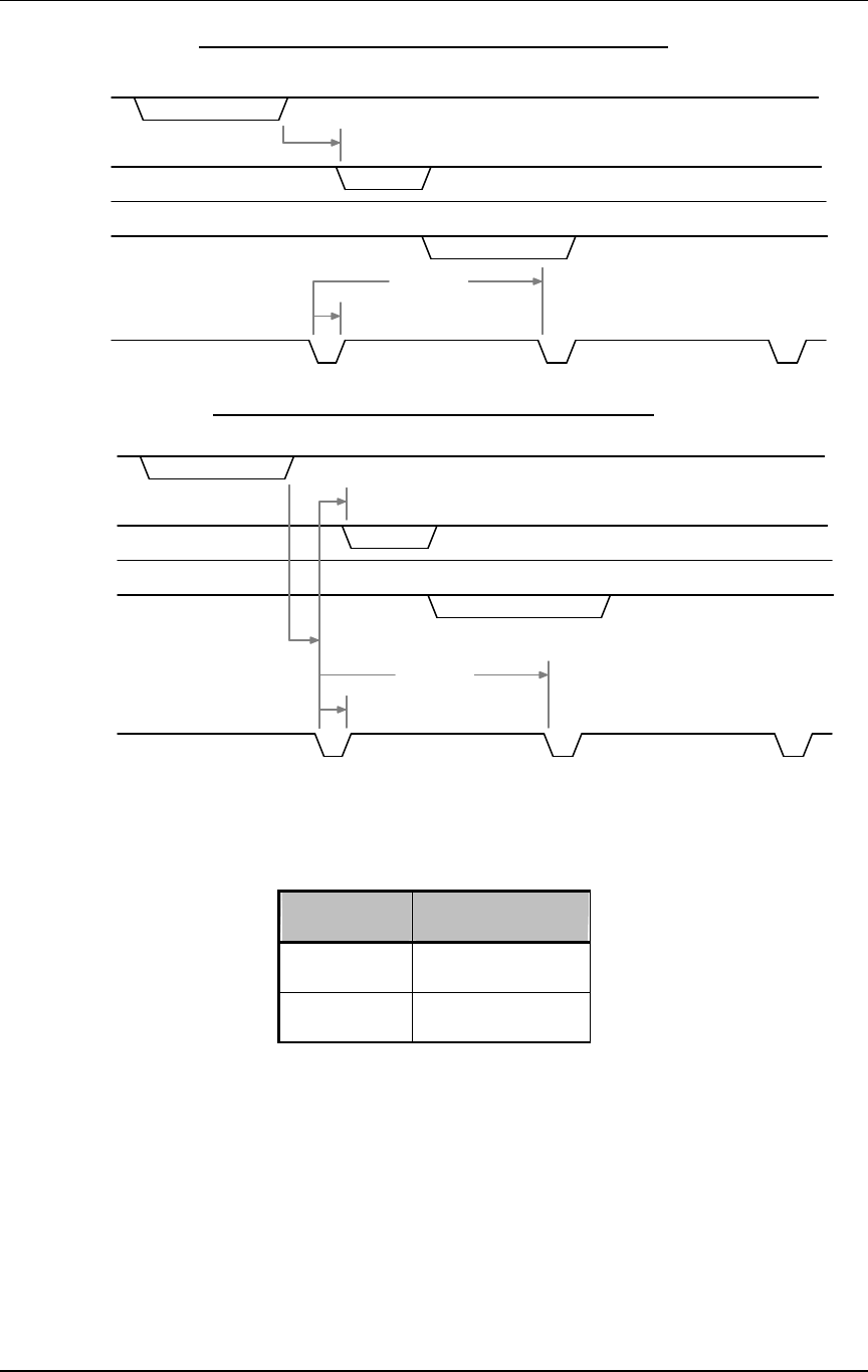
Addressed Acknowledge Mode with Interface Timeout:
Addressed Acknowledge Mode with No Interface Timeout:
Local_RXD
Local_RF_TXD
Remote_RF_TXD
Remote_TXD
Hop_Frame
Packet Data
RF Packet
Received Data
RF Acknowledge
Hop Time
Wait for Hop
Hop Period
Local_RXD
Local_RF_TXD
Remote_RF_TXD
Remote_TXD
Hop_Frame
Packet Data
RF Packet
Received Data
RF Acknowledge
Hop Time
Hop Period
Interface Timeout
Wait for Hop
Local_RXD
Local_RF_TXD
Remote_RF_TXD
Remote_TXD
Hop_Frame
Packet Data
Received Data
RF Packets
Hop Time
Wait for Hop
Hop Period
AC4490/AC4486 Specifications
11/07/03 13
Broadcast Acknowledge Mode with No Interface Timeout:
Broadcast Acknowledge Mode with Interface Timeout:
Table 6 – Timing Parameters
Parameter Typical Time (ms)
Hop Time 1
Hop Period 20
Local_RXD
Local_RF_TXD
Remote_RF_TXD
Remote_TXD
Hop_Frame
Packet Data
RF Packet
Received Data
Hop Time
Wait for Hop
Hop Period
Local_RXD
Local_RF_TXD
Remote_RF_TXD
Remote_TXD
Hop_Frame
Packet Data
RF Packet
Received Data
Hop Time
Hop Period
Interface Timeout
Wait for Hop

AC4490/AC4486 Specifications
11/07/03 14
3.3.3 Maximum Overall System Throughput
When configured as shown in the table below, an AC4490/AC4486 transceiver is capable of achieving
the listed throughput. However, in the presence of interference or at longer ranges, the transceiver
might not be able to meet these specified throughputs.
Table 7 – Maximum Overall System Throughputs
RF Mode One Beacon
Mode
Throughput (bps)
Half Duplex
Throughput (bps)
Full Duplex
Stream Disabled 57.6k N/A
Acknowledge
Enabled 48k 24k
Acknowledge
Disabled 38k 19k

AC4490/AC4486 Specifications
11/07/03 15
4. Configuring the AC4490
4.1 EEPROM PARAMETERS
A Host can program various parameters that are stored in EEPROM and become active after a power-
on reset. Table 7 - EEPROM Parameters, gives the locations and descriptions of the parameters that
can be read or written by a Host. Factory default values are also shown. Do not write to any EEPROM
addresses other than those listed below. Do not copy a transceiver’s EEPROM data to another
transceiver. Doing so may cause the transceiver to malfunction.
Table 8 – EEPROM Parameters
Parameter
EEPROM
Address
Length
(Bytes) Range Default Description
Product ID 00h 40
40 bytes - Product identifier string. Includes
revision information for software and
hardware.
Sub Hop Adjust
36h 1 00 – FFh
66h This value should only be changed when
recommended by Aerocomm
Range Refresh
3Dh 1 00 – FFh
18h
This byte specifies the maximum amount of
time a transceiver will report In Range
without having heard a beacon (320ms per
increment). 0h is actually 256 * 320ms.
Channel
Number 40h 1 00 – 39h 00h
Set 0 = 00 – 0Fh (US/Canada) – AC4490
Set 1 = 10 – 2Fh (US/Canada) – AC4490
Set 2 = 30 – 37h (Australia) – AC4490
Set 3 = 38h (Europe 500mW) – AC4486
Set 4 = 39h (Europe 5mW) – AC4486
Server/Client
Mode 41h 1 01 – 02h 02h 01h = Server
02h = Client
Baud Rate Low
42h 1 00 – FFh
FCh Low Byte of the interface baud rate.
Baud Rate High
43h 1 00h 00h Always 00h

AC4490/AC4486 Specifications
11/07/03 16
Parameter
EEPROM
Address
Length
(Bytes) Range Default Description
Control 0 45h 1 00010100b
(14h) Settings are:
Bit 7 – One Beacon
0 = Beacon every hop
1 = Beacon once per hop cycle
Bit 6 – AeroComm Use Only
Bit 5 – Sync to Channel
0 = Don't Sync to Channel
1 = Sync to Channel
Bit 4 – AeroComm Use Only
Bit 3 – AeroComm Use Only
Bit 2 – RF Mode
0 = RF Stream Mode
1 = RF Acknowledge Mode
Bit 1 – RF Delivery
0 = Addressed
1 = Broadcast
Bit 0 – AeroComm Use Only
Frequency
Offset 46h 1 00 – FFh
01h Protocol parameter used in conjunction with
Channel Number.
Transmit
Retries 4Ch 1 01 – FFh
10h Maximum number of times a packet is sent
out in Addressed Acknowledge mode.
Broadcast
Attempts 4Dh 1 01 – FFh
04h Number of times a packet is sent out in
Broadcast Acknowledge mode.
API Control 56h 1 01000011b
(43h) Settings are:
Bit 7 – AeroComm Use Only
Bit 6 – AeroComm Use Only
Bit 5 – Unicast Only
0 = Receive Unicast and Broadcast
packets
1 = Only receive Unicast packets
Bit 4 – Auto Destination
0 = Use Destination Address
1 = Set Destination to Server
Bit 3 – AeroComm Use Only
Bit 2 – RTS Enable
0 = RTS Ignored
1 = Transceiver obeys RTS
Bit 1 – Duplex Mode
0 = Half Duplex
1 = Full Duplex
Bit 0 – Auto Config
0 = Use EEPROM values
1 = Auto Configure Values
Interface
Timeout 58h 1 02 – FFh
04h
Specifies a byte gap timeout, used in
conjunction with RF Packet Size, to
determine when a packet is complete (0.5ms
per increment).
Sync Channel
5Ah 1 00 – 3Fh 01h Used to synchronize the hopping of
collocated systems to minimize interference.

AC4490/AC4486 Specifications
11/07/03 17
Parameter
EEPROM
Address
Length
(Bytes) Range Default Description
RF Packet Size
5Bh 1 01 – FFh
46h Specifies the maximum size of an RF
packet.
CTS On 5Ch 1 01 – FFh
D2h
CTS will be deasserted (High) when the
transmit buffer contains at least this many
characters.
CTS On
Hysteresis 5Dh 1 00 – FEh
ACh
Once CTS has been deasserted, CTS will be
reasserted (Low) when the transmit buffer
contains this many or less characters.
Max Power 63h 1 00 – FFh
60h Used to increase or decrease transmit
power output.
Modem Mode
6Eh 1 E3h, FFh
FFh E3h = Enable Modem Mode
FFh = Disable Modem Mode
Parity Mode 6Fh 1 E3h, FFh
FFh E3h = Enable Parity Mode
FFh = Disable Parity Mode
RS-485 DE 7Fh 1 E3h, FFh
FFh
E3h = GO0 is active Low DE for control of
external RS-485 hardware.
FFh = Disable RS-485 DE mode
Destination ID
70h 6 Specifies destination for RF packets.
System ID 76h 1 00 – FFh
01h Similar to a network password.
MAC ID 80h 6 Unique IEEE MAC Address.

AC4490/AC4486 Specifications
11/07/03 18
4.2 EEPROM CONFIGURATION COMMANDS
The configuration set allows the Host to modify the operation of the transceiver. If the Command/Data
pin (Pin 17) is pulled logic Low, a transceiver will interpret incoming Host data as Command Data. The
Host can then read and write parameters using the various configuration commands listed below. To
exit Configuration Mode, the Host must perform a hardware or power-on reset or issue an Exit
Command Mode command to the transceiver. While in Configuration Mode, the RF circuitry will be
disabled.
4.2.1 EEPROM Byte Read
Upon receiving this command, a transceiver will transmit the desired data from the address requested
by the Host.
Host Command:
Byte 1 = C0h
Byte 2 = Address
Byte 3 = Length (01…FFh = 1…255 bytes; 00h = 256 bytes)
Transceiver Response:
Byte 1 = C0h
Byte 2 = Address
Byte 3 = Length
Byte 4…n = Data at requested address(s)
4.2.2 EEPROM Byte Write
Upon receiving this command, a transceiver will write the data byte to the address specified but will not
echo it back to the Host until the EEPROM write cycle is complete. The write can take as long as
10ms to complete. Following the write cycle, a transceiver will transmit the data byte to the Host.
Multiple byte EEPROM writes are allowed up to a length of 128 bytes. An EEPROM boundary exists
between addresses 7Fh and 80h. No single EEPROM write command shall write to addresses on
both sides of that EEPROM boundary.
Host Command:
Byte 1 = C1h
Byte 2 = Address
Byte 3 = Length (01 – 80h)
Byte 4…n = Data to store at Address
Transceiver Response:
Byte 1 = C1h
Byte 2 = Address
Byte 3 = Length (01 – 80h)
Byte 4 = Last data byte written by this command

AC4490/AC4486 Specifications
11/07/03 19
4.2.3 EEPROM Exit Configuration Mode Command
The OEM Host can cause the transceiver to exit Configuration Mode by issuing the Exit Configuration
Mode command to the transceiver. However, the transceiver will not reflect any of the changes
programmed into the EEPROM until the transceiver is reset.
Host Command:
Byte 1 = 56h
Transceiver Response:
Byte 1 = 56h
4.3 AC4490 AT COMMANDS
The AT Command mode implemented in AC4490 firmware version 3.2 and higher creates a virtual
version of the Command/Data line. The Enter AT Command mode command asserts this virtual line
Low (to signify Command mode) and the Exit AT Command mode command asserts this virtual line
High (to signify Data mode). Once this line has been asserted Low, all on-the-fly CC Commands
documented in the manual are supported.
When in AT Command mode, the transceiver will maintain synchronization with the network, but RF
packets will not be received. However, an ambiguity of approximately 10ms exists where, if the Enter
AT Command mode command has been sent to the transceiver at the same time an RF packet is
being received, the RF packet could be sent to the OEM Host before the AT Command mode
command response is sent to the host.
4.3.1 Enter AT Command Mode
Prior to sending the Enter AT Command mode command to the transceiver, the host must ensure that
the RF transmit buffer of the transceiver is empty (if the buffer is not empty, the Enter AT Command
Mode command will be interpreted as packet data and transmitted out over the RF). This can be
accomplished by waiting up to one second between the last transmit packet and the AT Command.
The host must also ensure that the Fixed Packet Length for the transceiver is set to a minimum of six.
The Enter AT Command Mode command is as follows:
Host Command:
AT+++?
Hexadecimal Representation of the Command:
41h, 54h, 2Bh, 2Bh, 2Bh, 0Dh
Transceiver Response:
CCh COM
Hexadecimal Representation of the Command:
CCh, 43h, 4Fh, 4Dh

AC4490/AC4486 Specifications
11/07/03 20
4.3.2 Exit AT Command Mode
To exit AT Command mode, the OEM host should send the following command to the transceiver:
Host Command:
CCh ATO?
Hexadecimal Representation of the Command:
CCh, 41h, 54h, 4Fh, 0Dh
Transceiver Response:
CCh DAT
Hexadecimal Representation of the Command:
CCh, 44h, 41h, 54h
4.4 ON-THE-FLY CONTROL COMMAND REFERENCE (CC COMMAND MODE)
The AC4490/AC4486 transceiver contains static memory that holds many of the parameters that
control the transceiver operation. Using the “CC” command set allows many of these parameters to
be changed during system operation. Because the memory these commands affect is static, when
the transceiver is reset, these parameters will revert back to the settings stored in the EEPROM. Note:
Do not to modify undocumented static addresses as undesired operation may occur. All “CC”
commands must be issued from the Host to the transceiver with Command/Data (Pin 17) pulled logic
Low. To exit “CC” mode, simply take the Command/Data pin High.
While in CC Command mode, the RF interface of the radio is still active. Therefore, it can receive
packets from remote radios while in CC Command mode and forwards these to the OEM Host. The
transceiver uses Interface Timeout to determine when a CC Command is complete. Therefore, there
should be no delay between each character as it is sent from the OEM Host to the transceiver or the
transceiver will not recognize the command and will enter Configuration Mode by default. If the OEM
Host has sent a CC Command to the transceiver and a RF packet is received by the transceiver, the
transceiver will send the CC Command response to the OEM Host before sending the packet.
However, if a RF packet is received before the Interface Timeout expires on a CC Command, the
transceiver will send the packet to the host before sending the CC Command response.

AC4490/AC4486 Specifications
11/07/03 21
4.4.1 Status Request
The Host issues this command to request the status of the transceiver.
Host Command:
Byte 1 = CCh
Byte 2 = 00h
Byte 3 = 00h
Transceiver Response:
Byte 1 = CCh
Byte 2 = Firmware version number
Byte 3 = Data1
Where:
Data1 =
00 for Server in Normal Operation
01 for Client in Normal Operation
02 for Server in Acquisition Sync
03 for Client in Acquisition Sync
4.4.2 Change Channel without Forced Acquisition Sync
The Host issues this command to change the channel of the transceiver. The transceiver will not begin
acquisition sync until its Range Refresh timer expires; therefore it is recommended that the host uses
the Change Channel with Forced Acquisition Sync Command.
Host Command:
Byte 1 = CCh
Byte 2 = 01h
Byte 3 = RF Channel Number (Hexadecimal)
Transceiver Response:
Byte 1 = CCh
Byte 2 = RF Channel Number (Hexadecimal)
4.4.3 Change Channel with Forced Acquisition Sync
The Host issues this command to change the channel of the transceiver and force the transceiver to
immediately begin synchronization.
Host Command:
Byte 1 = CCh
Byte 2 = 02h
Byte 3 = RF Channel Number (Hexadecimal)
Transceiver Response:
Byte 1 = CCh
Byte 2 = RF Channel Number (Hexadecimal)

AC4490/AC4486 Specifications
11/07/03 22
4.4.4 Server/Client Command
The Host issues this command to change the mode (Server or Client) of the transceiver and can force
the transceiver to actively begin synchronization. The transceiver will not begin acquisition sync until
its Range Refresh timer expires; therefore it is recommended that the host uses the commands which
force acquisition sync.
Host Command:
Byte 1 = CCh
Byte 2 = 03h
Byte 3 = Data1
Where:
Data1 =
00 for Server in Normal Operation
01 for Client in Normal Operation
02 for Server in Acquisition Sync
03 for Client in Acquisition Sync
Transceiver Response:
Byte 1 = CCh
Byte 2 = Software Version Number
Byte 3 = Data1
Where:
Data1 = Data1 from Host Command
4.4.5 Sync to Channel Command
The Host issues this command to change the Sync Channel byte and enable Sync to Channel.
Host Command:
Byte 1 = CCh
Byte 2 = 05h
Byte 3 = Data1
Where:
Data1 = New Sync Channel
Transceiver Response:
Byte 1 = CCh
Byte 2 = 05h
Byte 3 = Data1
Where:
Data1 = Data1 from Host Command

AC4490/AC4486 Specifications
11/07/03 23
4.4.6 Sleep Walk Power-Down Command
After the Host issues the power-down command to the transceiver, the transceiver will de-assert the
In_Range line after entering power-down. A Client transceiver in power-down will remain in sync with a
Server for a minimum of 2 minutes. To maintain synchronization with the Server, this Client transceiver
should re-sync to the Server at least once every 2 minutes. This re-sync is accomplished by issuing
the Power-Down Wake-Up Command and waiting for the In Range line to go active. Once this occurs,
the Client transceiver is in sync with the Server and can be put back into power-down. This command
is only valid for Client radios.
Host Command:
Byte 1 = CCh
Byte 2 = 06h
Transceiver Response:
Byte 1 = CCh
Byte 2 = RF Channel Number
4.4.7 Sleep Walk Power-Down Wake-Up Command
The Power-Down Wake-Up Command is issued by the Host to bring the transceiver out of power-
down mode.
Host Command:
Byte 1 = CCh
Byte 2 = 07h
Transceiver Response:
Byte 1 = CCh
Byte 2 = RF Channel Number
4.4.8 Broadcast Mode
The Host issues this command to change the transceiver operation between Addressed Mode and
Broadcast Mode. If addressed mode is selected the transceiver will send all packets to the radio
designated by the Destination Address programmed in the transceiver.
Host Command:
Byte 1 = CCh
Byte 2 = 08h
Byte 3 = 00 for addressed mode, 01 for broadcast mode
Transceiver Response:
Byte 1 = CCh
Byte 2 = 00 for addressed mode, 01 for broadcast mode

AC4490/AC4486 Specifications
11/07/03 24
4.4.9 Read Static Bank #1 Byte
The OEM Host issues this command to the transceiver to read Static Bank #1 Bytes. Static Bank #1 is
a bank of memory that holds many of the parameters that control the radio. Using the Read/Write
Static Bank #1 command allows these parameters to be changed dynamically. Because the memory
bank is static, when the radio is reset, these parameters will revert back to the settings stored in
EEPROM. Be careful not to change undocumented Static Bank addresses as undesired operation
may occur.
Host Command:
Byte 1 = CCh
Byte 2 = 0Ah
Byte 3 = 00 – FFh corresponding to a valid Static Bank #1 address
Transceiver Response:
Byte 1 = CCh
Byte 2 = 00 – FFh corresponding to a valid Static Bank #1 address
4.4.10 Write Static Bank #1 Byte
The Host issues this command to the transceiver to write Static Bank #1 Bytes. Static Bank #1 is a
bank of memory that holds many of the parameters that control the radio. Using the Read/Write Static
Bank #1 command allows these parameters to be changed dynamically. Because the memory bank
is static, when the radio is reset, these parameters will revert back to the settings stored in EEPROM.
Be careful not to change undocumented Static Bank addresses as undesired operation may occur.
Host Command:
Byte 1 = CCh
Byte 2 = 0Bh
Byte 3 = 00 – FFh corresponding to a valid Static Bank #1 address
Byte 4 = 00 – FFh corresponding to new value for address specified by Byte 3
Transceiver Response:
Byte 1 = CCh
Byte 2 = 00 – FFh corresponding to a valid Static Bank #1 address
Byte 3 = 00 – FFh corresponding to new value for address specified by Byte 2
4.4.11 Read Static Bank #2 Byte
The Host issues this command to the transceiver to read Static Bank #2 Bytes. Static Bank #2 is a
bank of memory that holds many of the parameters that control the radio. Using the Read/Write Static
Bank #2 command allows these parameters to be changed dynamically. Because the memory bank
is static, when the radio is reset, these parameters will revert back to the settings stored in EEPROM.
Be careful not to change undocumented Static Bank addresses as undesired operation may occur.
Host Command:
Byte 1 = CCh
Byte 2 = 0Ch
Byte 3 = 00 – FFh corresponding to a valid Static Bank #2 address
Transceiver Response:
Byte 1 = CCh

AC4490/AC4486 Specifications
11/07/03 25
Byte 2 = 00 – FFh corresponding to a valid Static Bank #2 address

AC4490/AC4486 Specifications
11/07/03 26
4.4.12 Write Static Bank #2 Byte
The Host issues this command to the transceiver to write Static Bank #2 Bytes. Static Bank #2 is a
bank of memory that holds many of the parameters that control the radio. Using the Read/Write Static
Bank #2 command allows these parameters to be changed dynamically. Because the memory bank
is static, when the radio is reset, these parameters will revert back to the settings stored in EEPROM.
Be careful not to change undocumented Static Bank addresses as undesired operation may occur.
Host Command:
Byte 1 = CCh
Byte 2 = 0Dh
Byte 3 = 00 – FFh corresponding to a valid Static Bank #2 address
Byte 4 = 00 – FFh corresponding to new value for address specified by Byte 3
Transceiver Response:
Byte 1 = CCh
Byte 2 = 00 – FFh corresponding to a valid Static Bank #2 address
Byte 3 = 00 – FFh corresponding to new value for address specified by Byte 2
4.4.13 Write Destination Address
The Host issues this command to the transceiver to change the Destination Address. This is a very
powerful command that provides the OEM Host with a means for ad-hoc networking. Only the three
Least Significant Bytes of the MAC Address are used for packet delivery.
Host Command:
Byte 1 = CCh
Byte 2 = 10h
Bytes 3 – 5 = 00 – FFh corresponding the three LSB’s of the destination MAC Address
Transceiver Response:
Byte 1 = CCh
Bytes 2 – 4= 00 – FFh corresponding the three LSB’s of the destination MAC Address
4.4.14 Read Destination Address
The Host issues this command to the transceiver to read the Destination Address. This is a very
powerful command that provides the OEM Host with a means for ad-hoc networking. Only the three
Least Significant Bytes of the MAC Address are used for packet delivery.
Host Command:
Byte 1 = CCh
Byte 2 = 11h
Transceiver Response:
Byte 1 = CCh
Bytes 2 – 4= 00 – FFh corresponding the three LSB’s of the destination MAC Address

AC4490/AC4486 Specifications
11/07/03 27
4.4.15 Read Digital Inputs
The Host issues this command to read both digital input lines.
Host Command:
Byte 1 = CCh
Byte 2 = 20h
Transceiver Response:
Byte 1 = CCh
Byte 2 = Data1
Where:
Data1 = bit 0 – GI0, bit 1 – GI1
4.4.16 Read ADC
The Host issues this command to read any of the three onboard A/D converters. The equations for
converting these 10 bits into an analog value and subsequent temperature are as follows:
Analog Voltage = (10 bits / 3FFh) * 3.3V
Temperature (°C) = ((Analog Voltage - 0.3) / 0.01) - 30
Host Command:
Byte 1 = CCh
Byte 2 = 21h
Byte 3 = Data1
Where:
Data1 = 00h – AD In, 01h – Temperature (if equipped), 02h – RSSI
Transceiver Response:
Byte 1 = CCh
Byte 2 = Data1
Byte 3 = Data2
Where:
Data1 = MSB of requested 10 bit ADC value
Data2 = LSB of requested 10 bit ADC value

AC4490/AC4486 Specifications
11/07/03 28
4.4.17 Report Last Valid RSSI
As RSSI values are only valid when the local radio is receiving a RF packet from a remote radio,
instantaneous RSSI can be very tricky to use. Therefore, the transceiver stores the most recent valid
RSSI value. The Host issues this command to request that value. Note: This value will default to FFh
on a Client and 00h on a Server if no valid RSSI measurement has been made since power-up. To
convert this byte into an analog voltage, the following equation should be used:
8 bit RSSI Voltage = (8 bits / FFh) * 3.3V
Host Command:
Byte 1 = CCh
Byte 2 = 22h
Transceiver Response:
Byte 1 = CCh
Byte 2 = Data1
Where:
Data1 = Most significant 8 bits of last valid RSSI reading.
4.4.18 Write Digital Outputs
The Host issues this command to write both digital output lines to particular states.
Host Command:
Byte 1 = CCh
Byte 2 = 23h
Byte 3 = Data1
Where:
Data1 = bit 0 – GO0, bit 1 – GO1
Transceiver Response:
Byte 1 = CCh
Byte 2 = Data1
Where:
Data1 = Data1 from Host command

AC4490/AC4486 Specifications
11/07/03 29
4.4.19 Write DAC
The Host issues this command to write DA Out to a particular voltage. NOTE: DA Out is an unbuffered,
high impedance output and must be buffered by the OEM Host when used. The transceiver uses a
PWM (Pulse Width Modulator) to generate the analog voltage. The theory behind PWM is that a binary
pulse is generated with a fixed duty cycle and rate. As such, this pin toggles between High and Low.
This signal is filtered via an onboard R-C circuit and an analog voltage is generated. Duty Cycle
specifies the ratio of time in one cycle that the pulse spends High proportionate to the amount of time it
spends Low. So, with a duty cycle of 50% (80h), the pulse is High 50% of the time and Low 50% of the
time; therefore the analog voltage would be half of 3.3V or 1.15V. A broad filter has been implemented
on the transceiver and there is no advantage to using a slower update period. Generally, a faster
update period is preferred.
Host Command:
Byte 1 = CCh
Byte 2 = 24h
Byte 3 = Data1
Byte 4 = Data2
Where:
Data1 = Update Period where: TUpdate = (255 * (Data1 + 1)) / 14.7256+06
Data2 = Duty Cycle where: Vout = (Data2 / FFh) * 3.3V
Transceiver Response:
Byte 1 = CCh
Byte 2 = Data1
Byte 3 = Data2
Where:
Data1 = Data1 from Host Command
Data2 = Data2 from Host Command
4.4.20 Set Max Power
The Host Issues this command to limit the maximum transmit power emitted by the transceiver. This
can be useful to minimize current consumption and satisfy certain regulatory requirements.
Host Command:
Byte 1 = CCh
Byte 2 = 25h
Byte 3 = Data1
Where:
Data1 = New Max Power
Transceiver Response:
Byte 1 = CCh
Byte 2 = Data1
Where:
Data1 = Data1 from Host Command

AC4490/AC4486 Specifications
11/07/03 30
4.4.21 Transmit Buffer Empty
The Host issues this command to determine when the RF Transmit buffer is empty. The Host will not
receive the transceiver response until that time.
Host Command:
Byte 1 = CCh
Byte 2 = 30h
Transceiver Response:
Byte 1 = CCh
Byte 2 = 00h
4.4.22 Disable Sync to Channel
The Host issues this command to disable Sync to Channel mode.
Host Command:
Byte 1 = CCh
Byte 2 = 85h
Transceiver Response:
Byte 1 = CCh
Byte 2 = RF Channel Number
4.4.23 Deep Sleep Mode
The Host issues this command to put the transceiver into Deep Sleep mode. Once in Deep Sleep, the
transceiver disables all RF communications and will not respond to any further commands until being
reset or power cycled. This command is valid for both Servers and Clients.
Host Command:
Byte 1 = CCh
Byte 2 = 86h
Transceiver Response:
Byte 1 = CCh
Byte 2 = RF Channel Number
4.4.24 Reset Command
The Host issues this command to perform a soft reset of the transceiver. Any transceiver settings
modified by CC Commands will be overwritten by values stored in the EEPROM.
Host Command:
Byte 1 = CCh
Byte 2 = FFh
Transceiver Response:
There is no response from the transceiver

AC4490/AC4486 Specifications
11/07/03 31
5. Theory of Operation
5.1 HARDWARE INTERFACE
Below is a description of all hardware pins used to control the AC4490.
5.1.1 GIn (Generic Inputs 0 and 1) (pins 4 and 14 respectively) and GOn
(Generic Outputs 0 and 1) (pins 1 and 9 respectively)
Both GIn pins serve as generic input pins. Both GOn pins serve as generic output pins. Reading and
writing of these pins can be performed using CC Commands (details can be found in the On-the-Fly
Control Command Reference). These pins alternately serve as control pins when Modem Mode is
enabled in the EEPROM.
5.1.2 TXD (Transmit Data) and RXD (Receive Data) (pins 2 and 3 respectively)
Serial TTL
The AC4490/AC4486 accepts 3.3 or 5VDC TTL level asynchronous serial data (the 500mW radio ONLY
accepts 3.3V level signals) on the RXD pin and interprets that data as either Command Data or
Transmit Data. Data is sent from the transceiver to the OEM Host via the TXD pin.
RS-485
When equipped with an onboard RS-485 interface chip, TXD and RXD become the half duplex RS-485
pins. In this mode, the transceiver will be in listen mode except when it has data to send to the OEM
host. TXD is the noninverted representation of the data and RXD is a mirror image of TXD. The
transceiver will still use RTS (if enabled) in this mode.
5.1.3 Hop Frame (pin 6)
The AC4490 is a frequency hopping spread spectrum radio. Frequency hopping allows the system to
hop around interference in order to provide a better wireless link. Hop Frame transitions logic Low at
the start of a hop and transitions logic High at the completion of a hop. The OEM Host is not required
to monitor Hop Frame. The AC4486 is a single frequency radio, though it still generates a Hop Frame
signal every time it transmits a timing beacon.

AC4490/AC4486 Specifications
11/07/03 32
5.1.4 CTS Handshaking (pin 7)
The AC4490/AC4486 has an interface buffer size of 256 bytes. If the buffer fills up and more bytes are
sent to the transceiver before the buffer can be emptied, data loss will occur. The transceiver prevents
this loss by asserting CTS High as the buffer fills up and taking CTS Low as the buffer is emptied. CTS
On in conjunction with CTS On Hysteresis control the operation of CTS. CTS On specifies the amount
of bytes that must be in the buffer for CTS to be disabled (High). Even while CTS is disabled, the OEM
Host can still send data to the transceiver, but it should do so carefully. Once CTS is disabled, it will
remain disabled until the buffer is reduced to the size specified by CTS On Hysteresis.
5.1.5 RTS Handshaking (pin 8)
With RTS Mode disabled, the transceiver will send any received packet to the OEM Host as soon as
the packet is received. However, some OEM Hosts are not able to accept data from the transceiver all
of the time. With RTS Mode Enabled, the OEM Host can keep the transceiver from sending it a packet
by disabling RTS (logic High). Once RTS is enabled (logic Low), the transceiver can send packets to
the OEM Host as they are received. Note: Leaving RTS disabled for too long can cause data loss
once the transceiver’s receive buffer fills up.
5.1.6 9600 Baud (pin 12)
9600_BAUD – When pulled logic Low before applying power or resetting, the transceiver’s serial
interface is forced to a 9600, 8-N-1 (8 data bits, No parity, 1 stop bit) rate. To exit, the transceiver must
be reset or power-cycled with 9600_Baud logic High. This pin is used to recover transceivers from
unknown baud rates only. It should not be used in normal operation. Instead the transceiver Interface
Baud Rate should be programmed to 9600 baud if that rate is desired for normal operation.
5.1.7 RSSI (pin 13)
Instantaneous RSSI
Received Signal Strength Indicator is used by the Host as an indication of instantaneous signal
strength at the receiver. The Host must calibrate RSSI without a RF signal being presented to the
receiver. Calibration is accomplished by following the steps listed below to find a minimum and
maximum voltage value.
1) Power up only one Client (no Server) transceiver in the coverage area.
2) Measure the RSSI signal to obtain the minimum value with no other signal present.
3) Power up a Server. Make sure the two transceivers are in close proximity and measure
the Client’s peak RSSI once the Client reports In Range to obtain a maximum value at full
signal strength.

AC4490/AC4486 Specifications
11/07/03 33
Validated RSSI
As RSSI values are only valid when the local radio is receiving a RF packet from a remote radio,
instantaneous RSSI can be very tricky to use. Therefore, the transceiver stores the most recent valid
RSSI value. The Host issues the Report Last Good RSSI command to request that value (details can
be found in the On-the-Fly Control Command Reference). Validated RSSI is not available at the RSSI
pin.
Figure 1 – RSSI Voltage vs. Received Signal Strength
5.1.8 UP_Reset (pin 15)
UP_Reset provides a direct connection to the reset pin on the AC4490/AC4486 microprocessor and is
used to force a soft reset. To guarantee a valid power-up reset, this pin should never be tied Low on
power-up. For a valid power-on reset, reset must be High for a minimum of 10ms.
5.1.9 Command/Data (pin 17)
When logic High, the transceiver interprets incoming Host data as transmit data to be sent to other
transceivers and their Hosts. When logic Low, the transceiver interprets Host data as command data
(see section 4).
0
0.2
0.4
0.6
0.8
1
1.2
-105 -100 -95 -90 -85 -80 -75 -70 -65 -60 -55 -50
Signal at Receiver (dBm)
Voltage (VDC)

AC4490/AC4486 Specifications
11/07/03 34
5.1.10 AD In and DA Out (pins 18 and 19 respectively)
AD In and DA Out can be used as a cost savings to replace Analog-to-Digital and Digital-to-Analog
converter hardware. Reading and writing of these two pins locally can be performed using commands
found in the On-the-Fly Control Command Reference. Note: DA Out is an unbuffered, high impedance
output and must be buffered by the OEM Host when used.
5.1.11 In Range (pin 20)
The IN_RANGE pin at the connector will be driven logic Low when a Client is in range of a Server on
the same RF Channel and System ID. If a Client cannot hear a Server for the amount of time specified
by Range Refresh, it will drive the IN_RANGE pin logic High and enter a search mode looking for a
Server. As soon as it detects a Server, the IN_RANGE pin will be driven logic Low. A Server Host can
determine which Clients are in range by the Server’s Host software polling a Client’s Host. IN_RANGE
will always be Low on the Server.

AC4490/AC4486 Specifications
11/07/03 35
5.2 SOFTWARE PARAMETERS
Following is a description of all software parameters used to control the AC4490.
5.2.1 RF Architecture (Unicast/Broadcast)
The Server controls the system timing by sending out regular beacons (transparent to the transceiver
Host) which contain system timing information. This timing information synchronizes the Client radios
to the Server.
Each network should consist of only one Server. There should never be two Servers on the same RF
Channel Number in the same coverage area as the interference between the two Servers will severely
hinder RF communications.
The AC4490/AC4486 runs a Peer-to-Peer type architecture where all transceivers, whether Servers or
Clients, can communicate with all other transceivers. To prohibit transceivers from receiving broadcast
packets, Unicast Only can be enabled.
5.2.2 RF Mode
All radios located on the same network must use the same RF Mode.
RF Delivery Overview
All packets are sent out over the RF as either addressed or broadcast packets. Addressed packets are
only received by the radio specified by Destination Address. If addressed packets are desired, the
Destination Address should be programmed with the MAC ID of the destination radio. To simplify
EEPROM programming, Auto Destination can be enabled in Clients which allows the Client to
automatically set its Destination Address to the address of the Server. Broadcast packets are sent out
to every eligible transceiver on the network. If broadcast packets are desired, RF Delivery should be
set to Broadcast.
Acknowledge Mode
In Addressed Acknowledge Mode, the RF packet is sent out to the receiver designated by the
Destination Address. Transmit Retries is used to increase the odds of successful delivery to the
intended receiver. Transparent to the OEM Host, the sending transceiver will send the RF packet to
the intended receiver. If the receiver receives the packet free of errors, it will tell the sender. If the
sender does not receive this acknowledge, it will assume the packet was never received and retry the
packet. This will go on until the packet is successfully received or the transmitter exhausts all of its
retries. The received packet will only be sent to the OEM Host if and when it is received free of errors.
In Broadcast Acknowledge Mode, the RF packet is broadcast out to all eligible receivers on the
network. Broadcast Attempts is used to increase the odds of successful delivery to the intended
receiver(s). Transparent to the OEM Host, the sending transceiver will send the RF packet to the
intended receiver. If the receiver detects a packet error, it will throw out the packet. This will go on until
the packet is successfully received or the transmitter exhausts all of its attempts. Once the receiver
successfully receives the packet it will send the packet to the OEM Host. It will throw out any
duplicates caused by further Broadcast Attempts. The received packet will only be sent to the OEM
Host if it is received free of errors.

AC4490/AC4486 Specifications
11/07/03 36
Stream Mode
In Broadcast Stream mode, the RF packet is broadcast out to all eligible receivers on the network. In
Addressed Stream Mode, the RF packet is sent out to the receiver designated by the Destination
Address. The sending transceiver will send each RF packet out once. There are no retries on the
packet. Whether or not the packet contains errors, the receiver(s) will send the packet to the OEM
Host. In fact, if only part of the packet is able to be received, the transceiver will still send the partial
packet to the OEM Host. Note: Stream Mode is incompatible with Full Duplex Mode.
5.2.3 Sub Hop Adjust
Sub Hop Adjust is an AC4490/AC4486 protocol parameter and should only be modified at the
recommendation of Aerocomm.
5.2.4 Duplex Mode
In Half Duplex mode, the AC4490/AC4486 will send a packet out over the RF when it can. This can
cause packets sent at the same time by a Server and a Client to collide with each other over the RF.
To prevent this, Full Duplex Mode can be enabled. This mode restricts Clients to transmitting on odd
numbered frequency “bins” and the Server to transmitting on even frequency bins. Though the RF
hardware is still technically half duplex, it makes the radio seem full duplex. This can cause overall
throughputs to be cut in half. Note: All transceivers on the same network must have the same setting
for Full Duplex. Full Duplex mode is incompatible with Stream RF mode.
5.2.5 Interface Timeout/RF Packet Size
Interface Timeout, in conjunction with RF Packet Size, determines when a buffer of data will be sent out
over the RF as a complete RF packet based on whichever condition occurs first.
Interface Timeout – Interface Timeout specifies a maximum byte gap between consecutive bytes.
When that byte gap is exceeded, the bytes in the transmit buffer are sent out over the RF as a
complete packet. Interface timeout is adjustable in 1ms increments and has a tolerance of ?1ms.
Therefore, the Interface Timeout should be set to a minimum of 2. The default value for Interface
Timeout is 4 or 4ms.
RF Packet Size – When the amount of bytes in the transceiver transmit buffer equals RF Packet Size,
those bytes are sent out as a complete RF packet. Every packet the transceiver sends over the RF
contains extra header bytes not counted in the RF Packet Size. Therefore, it is much more efficient to
send a few large packets than to send many short packets. However, if RF Packet size is set too large
and Acknowledge Mode is enabled, the transceiver will not be able to send any packets because
Acknowledge Mode requires the entire RF packet to be sent in the same hop whereas Stream Mode
packets can span multiple hops.

AC4490/AC4486 Specifications
11/07/03 37
5.2.6 Serial Interface Baud Rate
This two-byte value determines the baud rate used for communicating over the serial interface to a
transceiver. Table 8 - Baud Rate/Timeout lists values for some common baud rates. Baud rates below
1200 baud are not supported. For a baud rate to be valid, the calculated baud rate must be within ?3%
of the OEM Host baud rate. If the 9600_BAUD pin (Pin 12) is pulled logic Low at reset, the baud rate
will be forced to 9,600. For Baud Rate values other than those shown in Table 5 - Baud Rate, the
following equation can be used:
BAUD = 100h - (14.7456E+06 / (64 * desired baud rate))
BaudH= Always 0
BaudL = Low 8 bits of BAUD (base16)
Table 9 – Baud Rate/Interface Timeout
Baud Rate
BaudL (42h)
BaudH (43h)
Minimum Interface Timeout (58h)
115,200 FEh 00h 02h
57,600 FCh 00h 02h
38,400 FAh 00h 02h
28,800 F8h 00h 02h
19,200 F4h 00h 02h
14,400 F0h 00h 03h
9,600 E8h 00h 03h
4800 D0h 00h 05h
2400 A0h 00h 09h
1200 40h 00h 11h
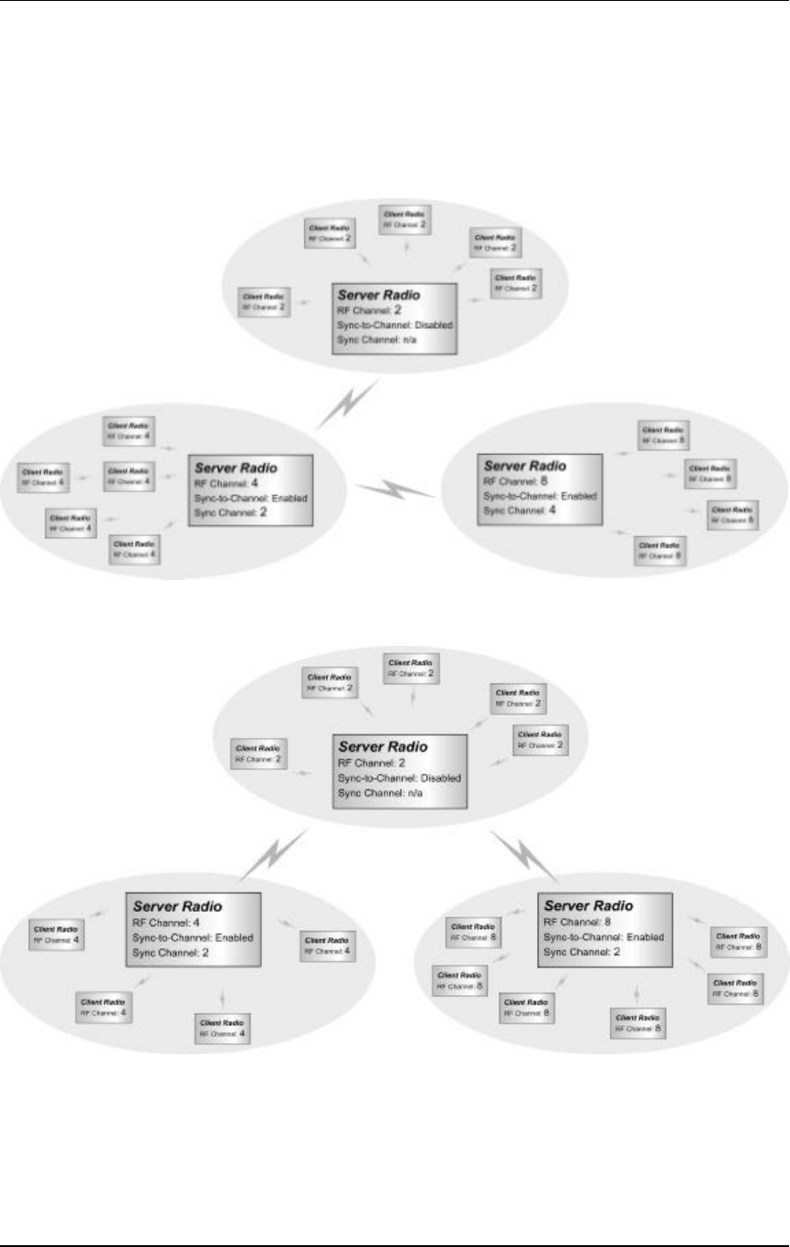
5.2.7 Network Topology
RF Channel Number – RF Channel Number provides a physical separation between collocated
networks. The AC4490 is a spread spectrum frequency hopping radio with a fixed hopping sequence.
Without synchronizing the different networks to each other, collocated systems on different channel
numbers can interfere with each other. To avoid this kind of interference, collocated networks can use
Sync-to-Channel. A Server radio with Sync-to-Channel enabled must have its Sync Channel set to
another Server’s RF Channel Number. It is required that a Server with Sync-to-Channel enabled must
have its Sync Channel set to a value less than its RF Channel Number. Collocated networks must use
the same Channel Set. See the Diagrams below:
AC4490/AC4486 Specifications
11/07/03 38
Daisy-Chain Network Configuration
Centralized Network Configuration
Frequency Offset – Frequency Offset is an AC4490/AC4486 protocol parameter used in conjunction
with RF Channel Number.
Table 10 – US and International RF Channel Number Settings

AC4490/AC4486 Specifications
11/07/03 39
Channel Set
RF Channel Number
Range (40h) Frequency Details and Regulatory
Requirements Countries
Frequency
Offset (46h)
0 (AC4490) 0 – 0Fh 902 – 928MHz (26 hop bins) US/Canada
1
1 (AC4490) 10 – 2Fh 902 – 928MHz (50 hop bins) US/Canada
N/A
2 (AC4490) 30 – 37h 915 – 928MHz Australia 0
3 (AC4486) 38h 869.4 –
869.65MHz (Up to 500mW at 10%
maximum transmit vs. receive duty cycle)
Europe 0
4 (AC4486) 39h 869.7 –
870MHz (Up to 5mW with no duty
cycle requirement) Europe 0
System ID – System ID is similar to a password character or network number and makes network
eavesdropping more difficult. A receiving radio will not go in range of or communicate with another
radio on a different System ID.
5.2.8 Auto Config
The AC4490/AC4486 has several variables that control its RF performance and vary by RF Mode and
RF Architecture. Enabling Auto Config will bypass the value for these variables stored in EEPROM and
use predetermined values for the given mode. Below is a list containing all of the variables affected by
Auto Config and their respective values (values are all in hexadecimal format). When Auto Config is
disabled, these values must be programmed in the radio EEPROM for the corresponding mode of
operation.

AC4490/AC4486 Specifications
11/07/03 40
Table 11 – Auto Config Parameters
Acknowledge Mode
Parameter (those not
named are
undocumented
protocol parameters)
EEPROM
Address Default
Stream Mode
One Beacon
Mode Disabled
One Beacon
Mode Enabled
Sub Hop Adjust 36 66 A0 A0 A0
47 0E 0E 0E 0E
48 90 90 90 90
4E 09 08 09 09
53 80 N/A3 80 80
54 07 07 07 07
RF Packet Size 5B 46 90 50 68
CTS On 5C D2 C0 DC DC
CTS On Hysteresis 5D AC BE B0 B0
5E 23 10 23 23
5F 08 08 08 08
5.2.9 One Beacon Mode
The beacon, which is sent by the Server and contains system timing information, takes approximately
1ms to send. Due to the protocol built into the AC4490, the transceiver can maintain perfect
synchronization even if it only hears a beacon once every two minutes. Normally the Server will send a
beacon once every hop. Enabling One Beacon mode causes the beacon to only be sent once per
complete hop cycle. Using this feature can make initial synchronization take slightly longer and can
make communications more difficult if operating on the fringe but can increase net throughput.
Range Refresh – The Server sends out timing beacons at regular intervals to maintain Client
synchronization. Upon hearing a beacon, a Client will be in range of the Server and will assert its
IN_RANGE pin Low. Each time the Client hears a Server beacon, it resets the Range Refresh timer. If
the timer ever expires the Client will be out of range, will take the IN_RANGE pin High and will enter
acquisition mode trying to find the Server again. Therefore, Range Refresh specifies the maximum
amount of time a Client can go without hearing a Server beacon. This variable is particularly useful
when operating on fringe coverage areas. The Range Refresh timer is equal to 320ms * the value of
Range Refresh. When One Beacon mode is enabled, it is recommended that Range Refresh be
increased from its default setting (testing might be required to determine the appropriate setting).
3 N/A: This parameter is not affected by Auto Config and the EEPROM value is used instead.

AC4490/AC4486 Specifications
11/07/03 41
5.2.10 Max Power
Max Power provides a means for controlling the RF transmit output power of the AC4490/AC4486.
The following table lists some common values for Max Power and their current consumption. Output
power and current consumption can vary by as much as ?10% per radio. Transmit power is shown
here in dBm (decibels per meter) and mW (milliwatts). The equations for converting between the two
are shown below:
Power (dBm) = 10 log10 Power (mW)
Power (mW) = 10^(Power (dBm) / 10)
able 12 – Max Power Settings for 100mW Transmitter
Max Power
(Address 63h) 100% Transmit
Current (mA) Transmit Power
Output(dBm) Transmit Power
Output (mW)
00h 47 -20 0.01
01h 50 -10 0.1
02h 50.5 -3 0.5
03h 52 1 1.26
04h 55 4 2.51
05h 58.5 7 5.01
06h 63.5 9 7.94
07h 69 10.5 11.22
08h 76 12 15.85
09h 83 13.5 22.39
0Ah 90.5 14.5 28.18
0Bh 97.5 15.5 35.48
0Ch 105 16.5 44.67
0Dh 111.5 17 50.12
0Eh 118 17.5 56.23
0Fh 123.5 18 63.1
1Eh 140.5 19 79.43
60h 156 20 100
Table 13 – Max Power Settings for 1000mW Transmitter
Max Power
(Address 63h) 100% Transmit
Current (mA) Transmit Power
Output(dBm) Transmit Power
Output (mW)
00h 310 -4.5 0.35
01h 320 6 3.98
02h 335 11.5 14.13
03h 345 14.5 28.18
04h 365 16.5 44.67
05h 395 18 63.1

AC4490/AC4486 Specifications
11/07/03 42
06h 440 19.5 89.13
07h 485 20.5 112.2
08h 525 22.5 177.83
09h 580 23.5 223.87
0Ah 620 24 251.19
0Bh 665 24.5 281.84
0Ch 695 25 316.23
0Dh 745 25.5 354.81
0Eh 810 26 398.11
0Fh 850 26.5 446.68
1Eh 880 27 501.19
60h 985 29.5 891.25
5.2.11 Interface Options
Modem Mode – Full modem handshaking is supported by the transceivers when enabled in EEPROM.
Modem Mode is incompatible with RS-485 DE mode. Because Command/Data performs an alternate
function when this mode is enabled, CC on-the-fly commands cannot be used and the only way to enter
Configuration Mode is by forcing 9600 baud through the 9600_BAUD pin. Therefore, modem mode,
though enabled in EEPROM, will be ignored when 9600 baud is forced. Both interfaces are shown below.

AC4490/AC4486 Specifications
11/07/03 43
Table 14 – Transceiver Interface to DCE (Server Radio)
When Interfacing the AC4490/AC4486 to a DCE (Data Communications Equipment):
DCE Pin
Number DCE Pin
Name Direction with
Respect to Radio AC4490/AC4486
Pin Name AC4490/AC4486
Pin Number
1 DCD In GI1 14
2 RXD In RXD 3
3 TXD Out TXD 2
4 DTR Out GO0 1
5 GND 5
6 DSR In Command/Data 17
7 RTS Out CTS 7
8 CTS In RTS 8
9 RI In GI0 4
Table 15 – Transceiver Interface to DTE (Client Radio)
When Interfacing the AC4490/AC4486 to a DTE (Data Terminal Equipment):
DTE Pin
Number DTE Pin
Name Direction with
Respect to Radio AC4490/AC4486
Pin Name AC4490/AC4486
Pin Number
1 DCD Out GO0 1
2 RXD Out TXD 2
3 TXD In RXD 3
4 DTR In GI0 4
5 GND 5
6 DSR Out Hop Frame 6
7 RTS In RTS 8
8 CTS Out CTS 7
9 RI Out GO1 9
RS-485 DE Control – When enabled in EEPROM, the transceiver will use the GO0 pin to control the DE
pin on external RS-485 circuitry. If enabled, when the transceiver has data to send to the host, it will
assert GO0 Low, send the data to the host, and take GO0 High.
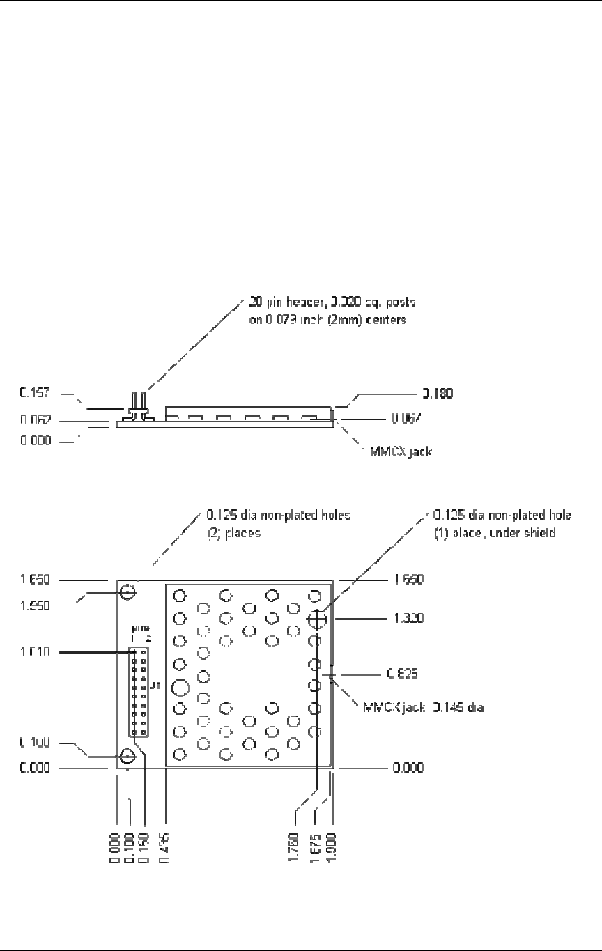
AC4490/AC4486 Specifications
11/07/03 44
6. Dimensions
Critical parameters are as follows:
Interface Connector – 20 pin OEM interface connector (Samtec TMM-110-01-L-D-SM, mates
with Samtec SMM-110-02-S-D)
MMCX Jack – Antenna connector (Telegartner P/N J01341C0081) mates with any
manufacturer’s MMCX plug
Figure 2 - AC4490/AC4486 (with MMCX Connector) Mechanical