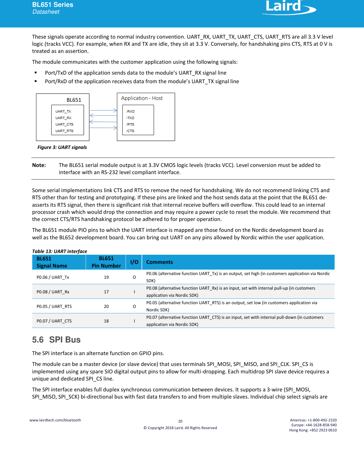
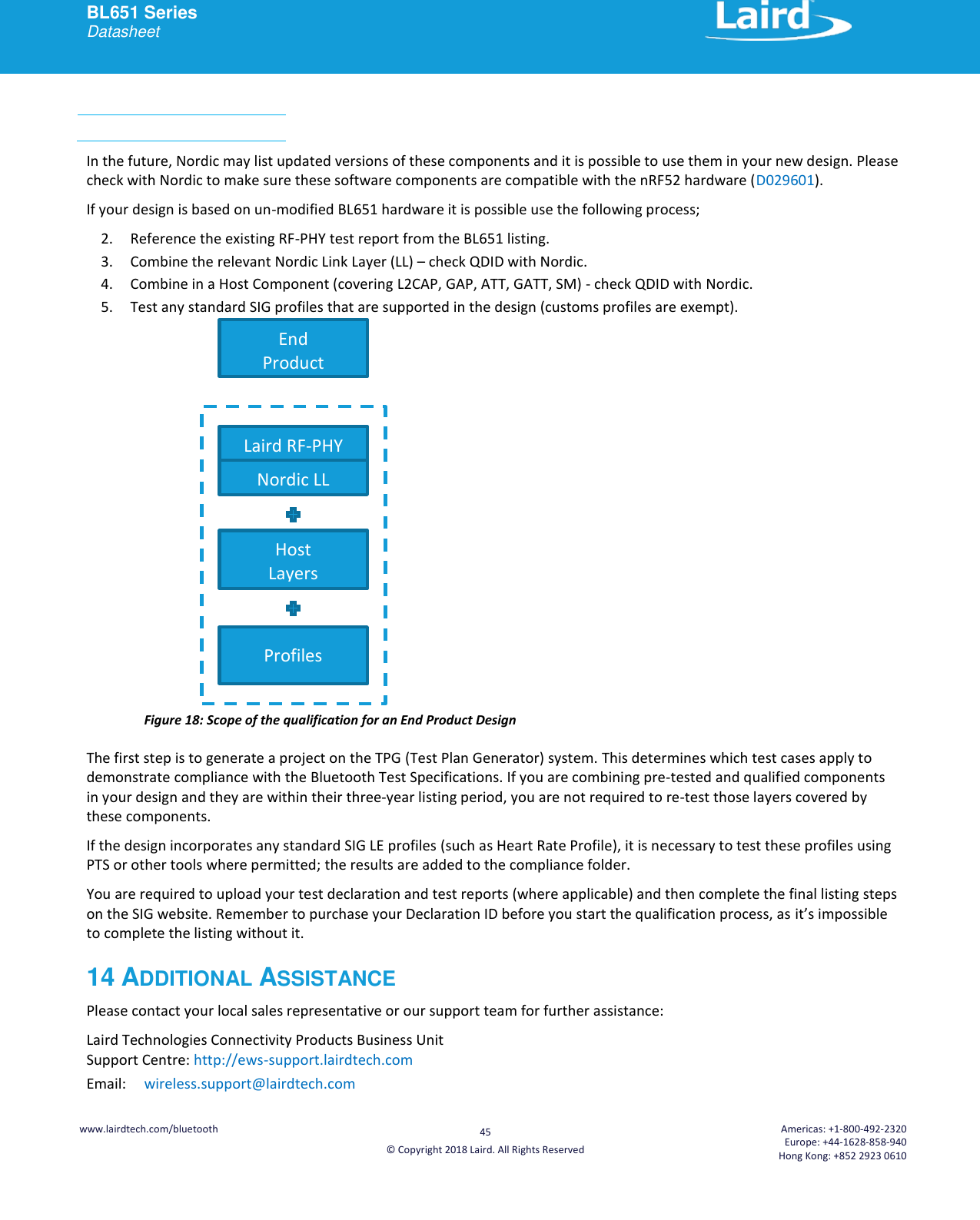
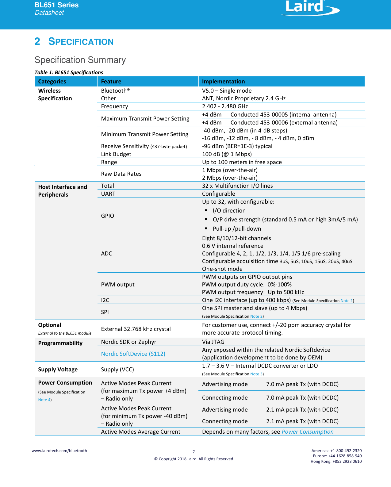
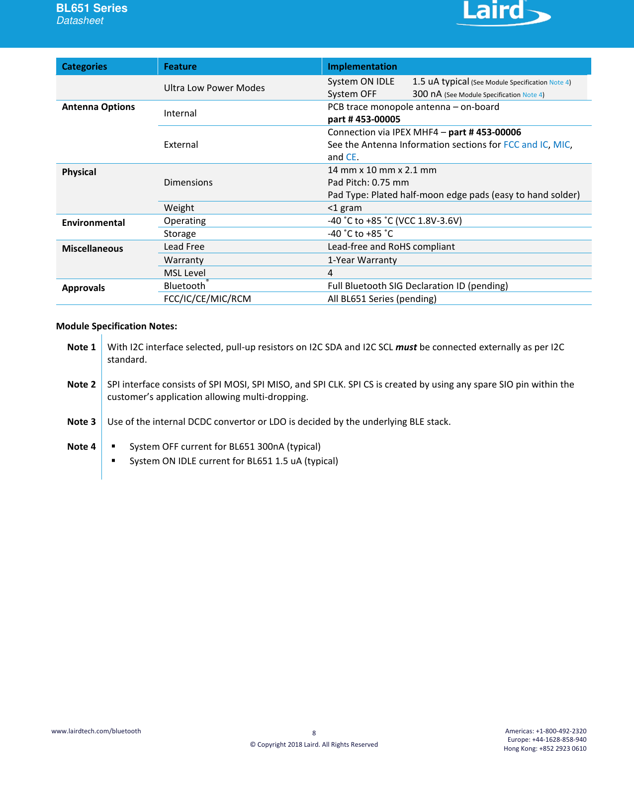
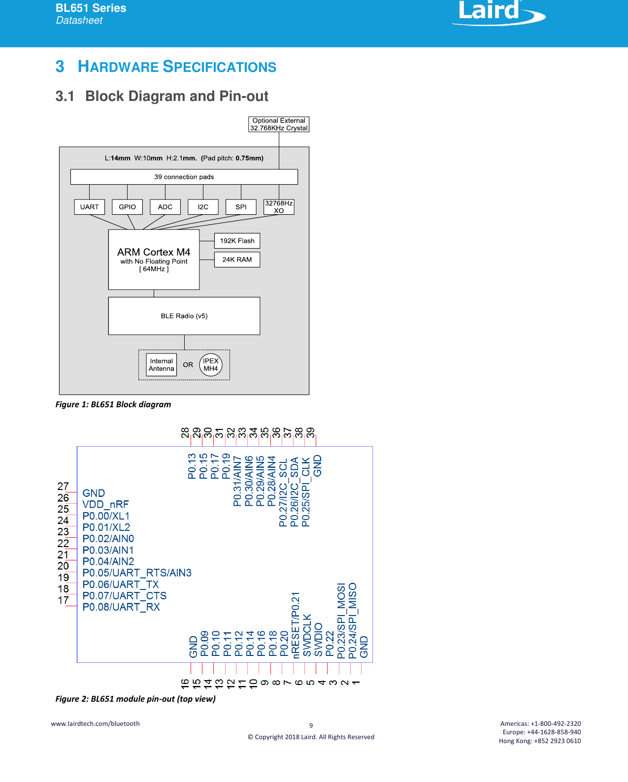
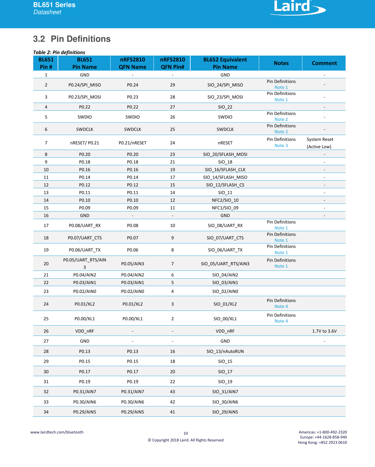
Laird Connectivity BL651 Bluetooth 5.0 Module w/Integrated PCB Antenna / Bluetooth 5.0 Module w/External Antenna User Manual
Laird Technologies Bluetooth 5.0 Module w/Integrated PCB Antenna / Bluetooth 5.0 Module w/External Antenna Users Manual
Users Manual
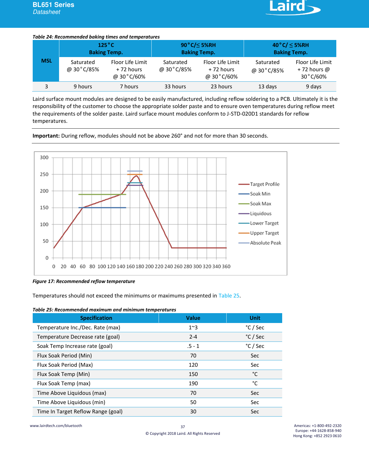
![BL651 Series Datasheet www.lairdtech.com/bluetooth 15 © Copyright 2018 Laird. All Rights Reserved Americas: +1-800-492-2320 Europe: +44-1628-858-940 Hong Kong: +852 2923 0610 4 POWER CONSUMPTION VCC_nRF of 3.0 V with internal (to chipset) LDO ON or with internal (to chipset) DCDC ON (see Power Consumption Note 1 ) and 25ºC. 4.1 Power Consumption Table 7: Power consumption Parameter Min Typ Max Unit Active mode ‘peak’ current (Power Consumption Note 1 ) (Advertising or Connection) Tx only run peak current @ Txpwr = +4 dBm Tx only run peak current @ Txpwr = 0 dBm Tx only run peak current @ Txpwr = -4 dBm Tx only run peak current @ Txpwr = -8 dBm Tx only run peak current @ Txpwr = -12 dBm Tx only run peak current @ Txpwr = -16 dBm Tx only run peak current @ Txpwr = -20 dBm Tx only run peak current @ Txpwr = -40 dBm With DCDC [with LDO] 7.0 [15.4] 4.6 [10.1] 3.6 [7.8] 3.2 [6.8] 2.9 [6.2] 2.7 [5.7] 2.5 [5.4] 2.1 [4.3] mA mA mA mA mA mA mA mA Active Mode (Power Consumption Note 1 ) Rx only ‘peak’ current 4.6 [10.0] mA Ultra-low Power Mode 1 (Power Consumption Note 2) System ON IDLE + 24kB RAM retention, wake on any event + LFRC 1.5 uA Ultra-low Power Mode 2 (Power Consumption Note 3) System OFF (no RAM retention, wake on any event) 300 nA Active Mode Average current Advertising Average Current draw Max, with advertising interval (min) 20 mS Min, with advertising interval (max)10240 mS Connection Average Current draw Max, with connection interval (min) 7.5 mS Min, with connection interval (max) 4000 mS (Power Cons. Note 4 ) (Power Cons. Note 4 ) dadf (Power Cons. Note 4 ) (Power Cons. Note 4 ) uA uA uA uA Power Consumption Notes: Note 1 This is for Peak Radio Current only, but there is additional current due to the MCU. The use of the internal DCDC convertor or LDO is decided by the underlying BLE stack. Note 2 BL651: System ON IDLE current is 1.5 uA typical. System ON IDLE is entered automatically through a command in the customer-developed firmware. In System ON IDLE, all enabled peripherals remain on and may re-awaken the chip. Depending on active peripherals, current consumption ranges from ~1.5 μA to 270 uA (when UART is ON). See individual peripherals current consumption data in the Peripheral Block Current Consumption section. Through customers FW development, functionality to detect GPIO change with no current consumption cost, it is possible to close the UART and get to the 1.5uA current consumption regime and still detect incoming data and be woken up so that the UART can be re-opened at expense of losing that first character. The BL651 System ON IDLE current consists of the below nRF52810 blocks:](https://usermanual.wiki/Laird-Connectivity/BL651/User-Guide-3980161-Page-15.png)