Laird Connectivity BL651 Bluetooth 5.0 Module w/Integrated PCB Antenna / Bluetooth 5.0 Module w/External Antenna User Manual
Laird Technologies Bluetooth 5.0 Module w/Integrated PCB Antenna / Bluetooth 5.0 Module w/External Antenna Users Manual
Users Manual

A
Datasheet
BL651 Series
Supports Laird Part Numbers:
453-00005
453-00006
453-00005C
453-00006C
Version 0.3
BL651 Series
Datasheet
www.lairdtech.com/bluetooth
2
© Copyright 2018 Laird. All Rights Reserved
Americas: +1-800-492-2320
Europe: +44-1628-858-940
Hong Kong: +852 2923 0610
REVISION HISTORY
Version
Date
Notes
Contributor(s)
Approver
0.x
27 June 2018
Initial Release
Andrew Chen
0.2
4 July 2018
updates
Raj Khatri
0.3
6-7August2018
Updated to close comments left
for me from review
Raj Khatri

BL651 Series
Datasheet
www.lairdtech.com/bluetooth
3
© Copyright 2018 Laird. All Rights Reserved
Americas: +1-800-492-2320
Europe: +44-1628-858-940
Hong Kong: +852 2923 0610
CONTENTS
1 Overview and Key Features ................................................................................................................................................. 6
1.1 Features and Benefits ................................................................................................................................................. 6
1.2 Application Areas ........................................................................................................................................................ 6
2 Specification ......................................................................................................................................................................... 7
Specification Summary ................................................................................................................................................................. 7
3 Hardware Specifications ...................................................................................................................................................... 9
3.1 Block Diagram and Pin-out ......................................................................................................................................... 9
3.2 Pin Definitions ........................................................................................................................................................... 10
3.3 Electrical Specifications ............................................................................................................................................ 11
3.3.1 Absolute Maximum Ratings ................................................................................................................................ 11
3.3.2 Recommended Operating Parameters ............................................................................................................... 12
4 Power Consumption........................................................................................................................................................... 15
4.1 Power Consumption ................................................................................................................................................. 15
4.2 Peripheral Block Current Consumption .................................................................................................................... 16
5 Functional Description ....................................................................................................................................................... 17
5.1 Power Management (includes Brown-out and Power on Reset) ............................................................................. 18
5.2 Clocks and Timers ..................................................................................................................................................... 19
5.2.1 Clocks .................................................................................................................................................................. 19
5.2.2 Timers ................................................................................................................................................................. 19
5.3 Memory .................................................................................................................................................................... 19
5.4 Radio Frequency (RF) ................................................................................................................................................ 19
5.5 UART Interface .......................................................................................................................................................... 19
5.6 SPI Bus....................................................................................................................................................................... 20
5.7 I2C Interface.............................................................................................................................................................. 21
5.8 General Purpose I/O, ADC, PWM, and FREQ ............................................................................................................ 21
5.8.1 GPIO .................................................................................................................................................................... 21
5.8.2 ADC ..................................................................................................................................................................... 22
5.8.3 PWM Signal Output on SIO Pins .......................................................................................................................... 22
5.9 nRESET pin ................................................................................................................................................................ 22
5.10 Two-wire Interface SWD ........................................................................................................................................... 23
5.11 BL651 Wakeup .......................................................................................................................................................... 24
5.11.1 Waking Up BL651 from Host ............................................................................................................................... 24
5.12 Low Power Modes .................................................................................................................................................... 24
5.13 Temperature Sensor ................................................................................................................................................. 24

BL651 Series
Datasheet
www.lairdtech.com/bluetooth
4
© Copyright 2018 Laird. All Rights Reserved
Americas: +1-800-492-2320
Europe: +44-1628-858-940
Hong Kong: +852 2923 0610
5.14 Security/Privacy ........................................................................................................................................................ 24
5.14.1 AES Encryption/Decryption ................................................................................................................................. 24
5.14.2 Readback Protection ........................................................................................................................................... 25
5.14.3 Elliptic Curve Cryptography................................................................................................................................. 25
5.15 Optional External 32.768 kHz Crystal ....................................................................................................................... 25
5.16 453-00005 On-board PCB Trace Antenna Characteristics ........................................................................................ 26
6 Hardware Integration Suggestions ..................................................................................................................................... 28
6.1 Circuit ........................................................................................................................................................................ 28
6.2 PCB Layout on Host PCB - General ............................................................................................................................ 29
6.3 PCB Layout on Host PCB for 453-00005 .................................................................................................................... 29
6.3.1 Antenna Keep-out on Host PCB .......................................................................................................................... 29
6.3.2 Antenna Keep-out and Proximity to Metal or Plastic ......................................................................................... 30
6.4 External Antenna Integration with 453-00006 ......................................................................................................... 30
7 Mechanical Details ............................................................................................................................................................. 31
7.1 BL651 Mechanical Details ......................................................................................................................................... 31
7.2 Host PCB Land Pattern and Antenna Keep-out for 453-00005 ................................................................................. 32
8 Application Note for Surface Mount Modules ................................................................................................................... 33
8.1 Introduction .............................................................................................................................................................. 33
8.2 Shipping .................................................................................................................................................................... 33
8.2.1 Tape and Reel Package Information ................................................................................................................... 33
8.2.2 Carton Contents .................................................................................................................................................. 34
8.2.3 Packaging Process ............................................................................................................................................... 35
8.2.4 Labeling ............................................................................................................................................................... 35
8.3 Reflow Parameters ................................................................................................................................................... 36
9 FCC and IC Regulatory ........................................................................................................................................................ 38
9.1 Antenna Information ................................................................................................................................................ 38
9.2 Power Exposure Information .................................................................................................................................... 39
9.3 OEM Responsibilities ................................................................................................................................................ 39
9.4 Federal Communication Commission Interference Statement ................................................................................ 39
9.5 Industry Canada Statement ...................................................................................................................................... 40
10 Japan (MIC) Regulatory ............................................................................................................................................. 42
10.1 Antenna Information ................................................................................................................................................ 42
11 CE Regulatory ............................................................................................................................................................ 42
11.1 Antenna Information ................................................................................................................................................ 42
11.2 EU Declarations of Conformity ................................................................................................................................. 43

BL651 Series
Datasheet
www.lairdtech.com/bluetooth
5
© Copyright 2018 Laird. All Rights Reserved
Americas: +1-800-492-2320
Europe: +44-1628-858-940
Hong Kong: +852 2923 0610
12 Ordering Information ................................................................................................................................................ 43
13 Bluetooth SIG Qualification ...................................................................................................................................... 44
13.1 Overview ................................................................................................................................................................... 44
13.2 Qualification Steps When Referencing a Laird End Product Design ......................................................................... 44
13.3 Qualification Steps When Deviating from a Laird End Product Design .................................................................... 44
14 Additional Assistance ................................................................................................................................................ 45
BL651 Series
Datasheet
www.lairdtech.com/bluetooth
6
© Copyright 2018 Laird. All Rights Reserved
Americas: +1-800-492-2320
Europe: +44-1628-858-940
Hong Kong: +852 2923 0610
1 OVERVIEW AND KEY FEATURES
Laird’s BL651 Series contains the latest Nordic nRF52810 silicon with Bluetooth 5 Low Energy, ANT and Proprietary 2.4
GHz capabilities and groundbreaking ultra-low power performance. Building on Laird’s multi-generation module
developments utilizing Nordic silicon (BL600, BL652, BL654) – now comes the latest series offering cost effective Bluetooth
5 enablement for simple BLE applications.
The BL651 series exposes all the capabilities of the Nordic nRF52810 silicon in a small, fully certified module with simple
soldering castellation for easy prototyping and mass production manufacturing. Use the Nordic SDK & SoftDevice to
deliver your BLE application. Let Laird’s innovative BL651 series and decades of expertise in Bluetooth module design speed
your product to market.
In addition, the BL651 series is 100% PCB footprint drop in compatible with the BL652 Series of modules.
1.1 Features and Benefits
Bluetooth v5.0 – Single mode
External or internal antennas
Application development via Nordic SDK or Zephyr
Compact footprint (pin compatible with BL652)
Programmable Tx power +4 dBm to -20 dBm
Tx whisper mode (-40 dBm)
Rx sensitivity: -96 dBm
Ultra-low power consumption
Tx: 4.6 mA peak (at 0 dBm, DCDC on) – See Power
Consumption section Note 1
Rx: 4.6 mA peak (DCDC on) – See Power Consumption
section Note 1
System ON IDLE: 1.5 uA typical
System OFF: 0.3 uA – See Power Consumption section
Note 4
UART, GPIO, ADC, PWM, timers, I2C, and SPI
interfaces
Fast time-to-market
FCC, CE, IC, and Japan certified; Full Bluetooth
Declaration ID
Other regulatory certifications on request (all
certifications are in process)
No external components required
Industrial temperature range (-40 to + 85)
1.2 Application Areas
Beacons
Computer peripherals
Home healthcare
Fitness sensors
IoT sensors
Home automation
Note: Figures on this page are gathered from the nRF52810 datasheet v1.2 provided by Nordic.
BL651 Series
Datasheet
www.lairdtech.com/bluetooth
7
© Copyright 2018 Laird. All Rights Reserved
Americas: +1-800-492-2320
Europe: +44-1628-858-940
Hong Kong: +852 2923 0610
2 SPECIFICATION
Specification Summary
Table 1: BL651 Specifications
Categories
Feature
Implementation
Wireless
Specification
Bluetooth®
Other
V5.0 – Single mode
ANT, Nordic Proprietary 2.4 GHz
Frequency
2.402 - 2.480 GHz
Maximum Transmit Power Setting
+4 dBm
Conducted 453-00005 (internal antenna)
+4 dBm
Conducted 453-00006 (external antenna)
Minimum Transmit Power Setting
-40 dBm, -20 dBm (in 4-dB steps)
-16 dBm, -12 dBm, - 8 dBm, - 4 dBm, 0 dBm
Receive Sensitivity (≤37-byte packet)
-96 dBm (BER=1E-3) typical
Link Budget
100 dB (@ 1 Mbps)
Range
Up to 100 meters in free space
Raw Data Rates
1 Mbps (over-the-air)
2 Mbps (over-the-air)
Host Interface and
Peripherals
Total
32 x Multifunction I/O lines
UART
Configurable
GPIO
Up to 32, with configurable:
I/O direction
O/P drive strength (standard 0.5 mA or high 3mA/5 mA)
Pull-up /pull-down
ADC
Eight 8/10/12-bit channels
0.6 V internal reference
Configurable 4, 2, 1, 1/2, 1/3, 1/4, 1/5 1/6 pre-scaling
Configurable acquisition time 3uS, 5uS, 10uS, 15uS, 20uS, 40uS
One-shot mode
PWM output
PWM outputs on GPIO output pins
PWM output duty cycle: 0%-100%
PWM output frequency: Up to 500 kHz
I2C
One I2C interface (up to 400 kbps) (See Module Specification Note 1)
SPI
One SPI master and slave (up to 4 Mbps)
(See Module Specification Note 2)
Optional
External to the BL651 module
External 32.768 kHz crystal
For customer use, connect +/-20 ppm accuracy crystal for
more accurate protocol timing.
Programmability
Nordic SDK or Zephyr
Via JTAG
Nordic SoftDevice (S112)
Any exposed within the related Nordic Softdevice
(application development to be done by OEM)
Supply Voltage
Supply (VCC)
1.7 – 3.6 V – Internal DCDC converter or LDO
(See Module Specification Note 3)
Power Consumption
(See Module Specification
Note 4)
Active Modes Peak Current
(for maximum Tx power +4 dBm)
– Radio only
Advertising mode
7.0 mA peak Tx (with DCDC)
Connecting mode
7.0 mA peak Tx (with DCDC)
Active Modes Peak Current
(for minimum Tx power -40 dBm)
– Radio only
Advertising mode
2.1 mA peak Tx (with DCDC)
Connecting mode
2.1 mA peak Tx (with DCDC)
Active Modes Average Current
Depends on many factors, see Power Consumption
BL651 Series
Datasheet
www.lairdtech.com/bluetooth
8
© Copyright 2018 Laird. All Rights Reserved
Americas: +1-800-492-2320
Europe: +44-1628-858-940
Hong Kong: +852 2923 0610
Categories
Feature
Implementation
Ultra Low Power Modes
System ON IDLE
System OFF
1.5 uA typical (See Module Specification Note 4)
300 nA (See Module Specification Note 4)
Antenna Options
Internal
PCB trace monopole antenna – on-board
part # 453-00005
External
Connection via IPEX MHF4 – part # 453-00006
See the Antenna Information sections for FCC and IC, MIC,
and CE.
Physical
Dimensions
14 mm x 10 mm x 2.1 mm
Pad Pitch: 0.75 mm
Pad Type: Plated half-moon edge pads (easy to hand solder)
Weight
<1 gram
Environmental
Operating
-40 ˚C to +85 ˚C (VCC 1.8V-3.6V)
Storage
-40 ˚C to +85 ˚C
Miscellaneous
Lead Free
Lead-free and RoHS compliant
Warranty
1-Year Warranty
MSL Level
4
Approvals
Bluetooth®
Full Bluetooth SIG Declaration ID (pending)
FCC/IC/CE/MIC/RCM
All BL651 Series (pending)
Module Specification Notes:
Note 1
With I2C interface selected, pull-up resistors on I2C SDA and I2C SCL must be connected externally as per I2C
standard.
Note 2
SPI interface consists of SPI MOSI, SPI MISO, and SPI CLK. SPI CS is created by using any spare SIO pin within the
customer’s application allowing multi-dropping.
Note 3
Use of the internal DCDC convertor or LDO is decided by the underlying BLE stack.
Note 4
System OFF current for BL651 300nA (typical)
System ON IDLE current for BL651 1.5 uA (typical)
BL651 Series
Datasheet
www.lairdtech.com/bluetooth
9
© Copyright 2018 Laird. All Rights Reserved
Americas: +1-800-492-2320
Europe: +44-1628-858-940
Hong Kong: +852 2923 0610
3 HARDWARE SPECIFICATIONS
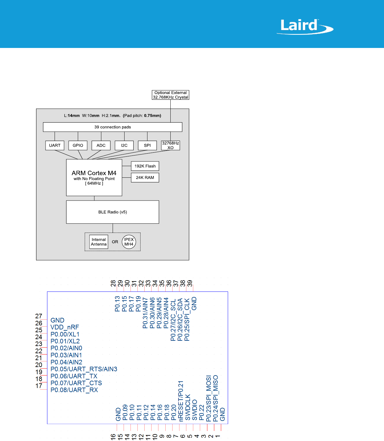
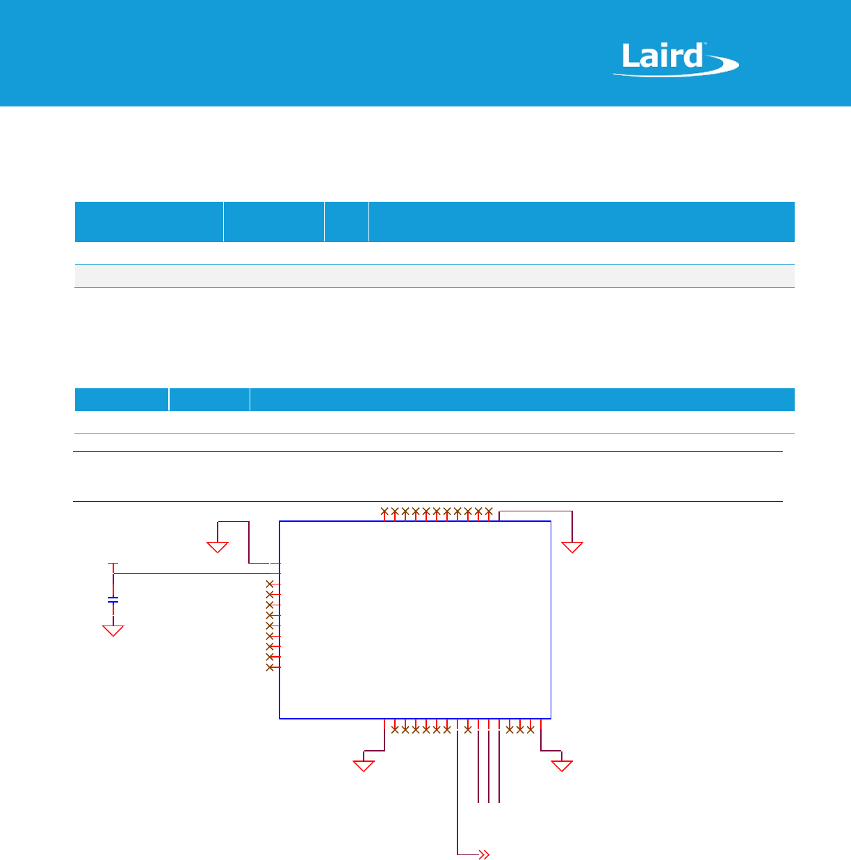
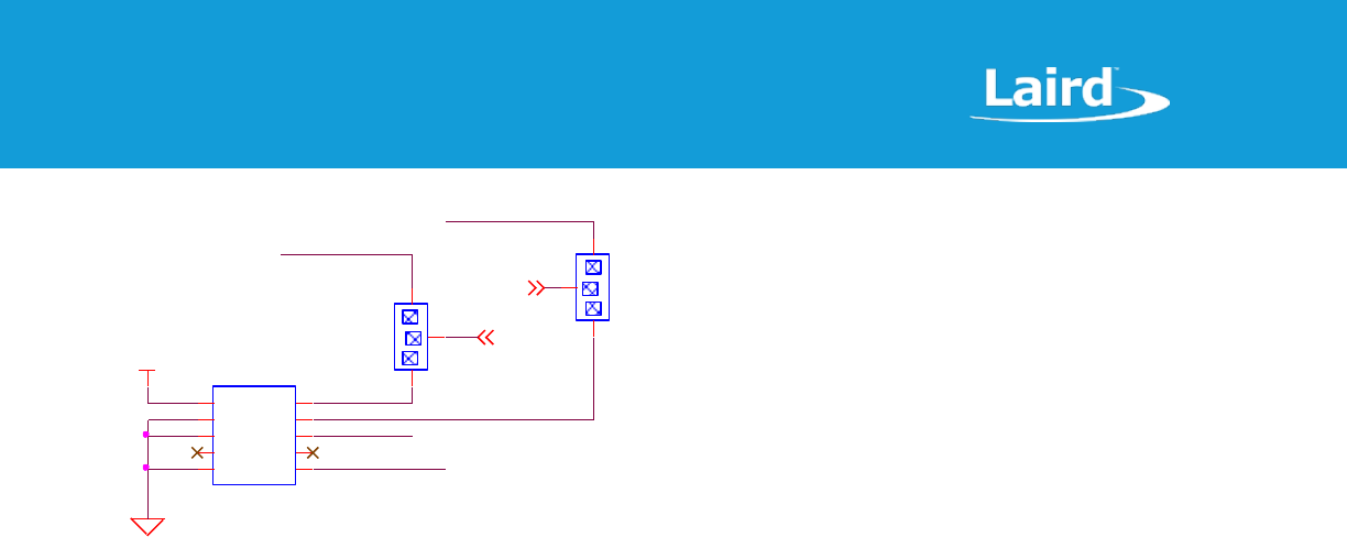
3.1 Block Diagram and Pin-out
Figure 1: BL651 Block diagram
Figure 2: BL651 module pin-out (top view)
BL651 Series
Datasheet
www.lairdtech.com/bluetooth
10
© Copyright 2018 Laird. All Rights Reserved
Americas: +1-800-492-2320
Europe: +44-1628-858-940
Hong Kong: +852 2923 0610
3.2 Pin Definitions
Table 2: Pin definitions
BL651
Pin #
BL651
Pin Name
nRF52810
QFN Name
nRF52810
QFN Pin#
BL652 Equivalent
Pin Name
Notes
Comment
1
GND
-
-
GND
-
2
P0.24/SPI_MISO
P0.24
29
SIO_24/SPI_MISO
Pin Definitions
Note 1
-
3
P0.23/SPI_MOSI
P0.23
28
SIO_23/SPI_MOSI
Pin Definitions
Note 1
-
4
P0.22
P0.22
27
SIO_22
-
5
SWDIO
SWDIO
26
SWDIO
Pin Definitions
Note 2
-
6
SWDCLK
SWDCLK
25
SWDCLK
Pin Definitions
Note 2
-
7
nRESET/ P0.21
P0.21/nRESET
24
nRESET
Pin Definitions
Note 3
System Reset
(Active Low)
8
P0.20
P0.20
23
SIO_20/SFLASH_MOSI
-
9
P0.18
P0.18
21
SIO_18
-
10
P0.16
P0.16
19
SIO_16/SFLASH_CLK
-
11
P0.14
P0.14
17
SIO_14/SFLASH_MISO
-
12
P0.12
P0.12
15
SIO_12/SFLASH_CS
-
13
P0.11
P0.11
14
SIO_11
-
14
P0.10
P0.10
12
NFC2/SIO_10
-
15
P0.09
P0.09
11
NFC1/SIO_09
-
16
GND
-
-
GND
-
17
P0.08/UART_RX
P0.08
10
SIO_08/UART_RX
Pin Definitions
Note 1
18
P0.07/UART_CTS
P0.07
9
SIO_07/UART_CTS
Pin Definitions
Note 1
19
P0.06/UART_TX
P0.06
8
SIO_06/UART_TX
Pin Definitions
Note 1
20
P0.05/UART_RTS/AIN
3
P0.05/AIN3
7
SIO_05/UART_RTS/AIN3
Pin Definitions
Note 1
21
P0.04/AIN2
P0.04/AIN2
6
SIO_04/AIN2
22
P0.03/AIN1
P0.03/AIN1
5
SIO_03/AIN1
23
P0.02/AIN0
P0.02/AIN0
4
SIO_02/AIN0
24
P0.01/XL2
P0.01/XL2
3
SIO_01/XL2
Pin Definitions
Note 4
25
P0.00/XL1
P0.00/XL1
2
SIO_00/XL1
Pin Definitions
Note 4
26
VDD_nRF
-
-
VDD_nRF
1.7V to 3.6V
27
GND
-
-
GND
-
28
P0.13
P0.13
16
SIO_13/nAutoRUN
29
P0.15
P0.15
18
SIO_15
30
P0.17
P0.17
20
SIO_17
31
P0.19
P0.19
22
SIO_19
32
P0.31/AIN7
P0.31/AIN7
43
SIO_31/AIN7
33
P0.30/AIN6
P0.30/AIN6
42
SIO_30/AIN6
34
P0.29/AIN5
P0.29/AIN5
41
SIO_29/AIN5
BL651 Series
Datasheet
www.lairdtech.com/bluetooth
11
© Copyright 2018 Laird. All Rights Reserved
Americas: +1-800-492-2320
Europe: +44-1628-858-940
Hong Kong: +852 2923 0610
BL651
Pin #
BL651
Pin Name
nRF52810
QFN Name
nRF52810
QFN Pin#
BL652 Equivalent
Pin Name
Notes
Comment
35
P0.28/AIN4
P0.28/AIN4
40
SIO_28/AIN4
36
P0.27/I2C_SCL
P0.27
39
SIO_27/I2C_SCL
Pin Definitions
Note 1
37
P0.26/I2C_SDA
P0.26
38
SIO_26/I2C_SDA
Pin Definitions
Note 1
38
P0.25/SPI_CLK
P0.25
37
SIO_25/SPI_CLK
Pin Definitions
Note 1
39
GND
-
-
GND
-
Pin Definition Notes:
Note 1
The BL651 module PIO pins to which UART, I2C, and SPI interfaces are mapped, are those found on the Nordic
development board as well as the BL652 development board. You can bring out UART, I2C, and SPI on any pins
allowed by Nordic within the user developed application.
Note 2
SWD (two-wire interface), pin 5 (SWDIO) and pin 6 (SWDCLK).
We recommend that you use SWD (2-wire interface) to handle customer developed BL651 module firmware
upgrades. You MUST wire out the SWD (2-wire interface) on your host design (see Figure 4, where four lines
should be wired out, namely SWDIO, SWDCLK, GND and VCC).
Note 3
Pull the nRESET pin (pin 7) low for a minimum of 100 milliseconds to reset the BL651.
Note 4
Not required for BL651 module normal operation. Nordic SDK examples by default assume that the external
32.768 kHz crystal is connected. You must modify the Nordic SDK example to reflect if the external 32.768 kHz
crystal is fitted or not. The on-chip 32.768 kHz RC oscillator provides the standard accuracy of ±500 ppm, with
calibration required at least every eight seconds to stay within ±500 ppm.
BL651 also allows the option of connecting an external higher accuracy (±20 ppm) 32.768 kHz crystal to the
BL651 pins SIO_01/XL2 (pin 24) and SIO_00/XL1 (pin 25). This provides higher accuracy protocol timing and
helps with radio power consumption in the SYSTEM ON IDLE or SYSTEM OFF modes by reducing the time that
the Rx window must be open.
3.3 Electrical Specifications
3.3.1 Absolute Maximum Ratings
Absolute maximum ratings for supply voltage and voltages on digital and analogue pins of the module are listed in Table 3.
Exceeding these values causes permanent damage.
Table 3: Maximum current ratings
Parameter
Min
Max
Unit
Voltage at VDD_nRF pin
-0.3
+3.9
(Maximum Ratings Note 1)
V
Voltage at GND pin
0
V
Voltage at GPIO pin (at VDD_nRF≤3.6V)
-0.3
VDD_nRF +0.3
V
Voltage at GPIO pin (at VDD_nRF≥3.6V)
-0.3
3.9
V
Radio RF input level
-
10
dBm
Environmental
Storage temperature
-40
+85
ºC
MSL (Moisture Sensitivity Level)
-
4
-
BL651 Series
Datasheet
www.lairdtech.com/bluetooth
12
© Copyright 2018 Laird. All Rights Reserved
Americas: +1-800-492-2320
Europe: +44-1628-858-940
Hong Kong: +852 2923 0610
Parameter
Min
Max
Unit
ESD (as per EN301-489)
Conductive
Air Coupling
4
8
KV
KV
Flash Memory (Endurance)
(Maximum Ratings Note 2)
-
10000
Write/erase cycles
Flash Memory (Retention)
-
10 years at 40°C
-
Maximum Ratings Notes:
Note 1
The absolute maximum rating for VCC pin (max) is 3.9V for the BL651.
Note 2
Standard wear levelling techniques can be used to increase the lifetime of the module.
3.3.2 Recommended Operating Parameters
Table 4: Power supply operating parameters
Parameter
Min
Typ
Max
Unit
VDD_nRF (independent of DCDC)
(Recommended Operating Parameters Note 1 )
1.7
3.0
3.6
V
VCC Maximum ripple or noise
(Recommended Operating Parameters Note 2 )
-
-
10
mV
VCC rise time (0 to 1.7V)
(Recommended Operating Parameters Note 3 )
-
-
60
mS
Operating Temperature Range
-40
-
+85
ºC
Recommended Operating Parameters Notes:
Note 1
4.7 uF internal to module on VCC.
Note 2
This is the maximum VCC ripple or noise (at any frequency) that does not disturb the radio.
Note 3
The on-board power-on reset circuitry may not function properly for rise times outside the noted interval.
Table 5: Signal levels for digital IO interfaces
Parameter
Min
Typ
Max
Unit
VIH Input high voltage
0.7 VDD_nRF
VDD_nRF
V
VIL Input low voltage
VSS
0.3 x VDD_nRF
V
VOH Output high voltage
(standard drive, 0.5 mA, VDD_nRF≥1.7V)
(high-drive, 3 mA, VDD_nRF≥1.7V)
(high-drive, 5 mA, VDD_nRF≥2.7V)
VDD_nRF -0.4
VDD_nRF -0.4
VDD_nRF -0.4
VDD_nRF
VDD_nRF
VDD_nRF
V
V
VOL Output low voltage
(standard drive, 0.5 mA, VDD_nRF≥1.7V)
(high-drive, 3 mA, VDD_nRF≥1.7V)
(high-drive, 5 mA, VDD_nRF≥2.7V)
VSS
VSS
VSS
VSS+0.4
VSS+0.4
VSS+0.4
V
V
VOL Current at VSS+0.4V, output set low
(standard drive, 0.5 mA, VDD_nRF≥1.7V)
1
2
4
mA
BL651 Series
Datasheet
www.lairdtech.com/bluetooth
13
© Copyright 2018 Laird. All Rights Reserved
Americas: +1-800-492-2320
Europe: +44-1628-858-940
Hong Kong: +852 2923 0610
Parameter
Min
Typ
Max
Unit
(high-drive, 3 mA, VDD_nRF≥1.7V)
(high-drive, 5 mA, VDD_nRF≥2.7V)
3
6
-
10
-
15
mA
mA
VOL Current at VDD_nRF -0.4, output set high
(standard drive, 0.5mA, VDD_nRF≥1.7V)
(high-drive, 3mA, VDD_nRF≥1.7V)
(high-drive, 5mA, VDD_nRF≥2.7V)
1
3
6
2
-
9
4
-
14
mA
mA
mA
Pull up resistance
11
13
16
kΩ
Pull down resistance
11
13
16
kΩ
Pad capacitance
3
pF
Table 6: AIN (ADC) specification
Parameter
Min
Typ
Max
Unit
ADC Internal reference voltage
-1.5%
0.6 V
+1.5%
%
ADC pin input internal selectable scaling
4, 2, 1, 1/2, 1/3, 1/4, 1/5 1/6
scaling
ADC input pin (AIN) voltage maximum without damaging ADC
w.r.t
(Recommended Operating Parameters Note 1 )
VCC Prescaling
0V-VDD_nRF 4, 2, 1, ½ , 1/3, ¼ , 1/5, 1/6
VDD_nRF + 0.3
V
Configurable
8-bit mode
10-bit mode
12-bit mode
bits
Acquisition Time, source resistance ≤10 kΩ Acquisition Time,
source resistance ≤40 kΩ
Acquisition Time, source resistance ≤100 kΩ
Acquisition Time, source resistance ≤200 kΩ
Acquisition Time, source resistance ≤400 kΩ
Acquisition Time, source resistance ≤800 kΩ
3
5
10
15
20
40
uS
uS
uS
uS
uS
uS
Conversion Time3
<2
uS
ADC input impedance (during operation)
(Recommended Operating Parameters Note 3
Input Resistance
Sample and hold capacitance at maximum gain
>1
2.5
MOhm
pF
Recommended Operating Parameters Notes:
Note 1
Stay within internal 0.6 V reference voltage with given pre-scaling on AIN pin and do not violate ADC maximum
input voltage (for damage) for a given VCC, e.g. If VCC is 3.6V, you can only expose AIN pin to VDD+0.3 V.
Note 2
Through customer firmware the resolution (8-bit, 10-bit, or 12-bit mode or oversample 14-bit) and acquisition
time is configurable. The sampling frequency is limited by the sum of sampling time and acquisition time. The
maximum sampling time is 2us. For acquisition time of 3us the total conversion time is 5us, which makes
maximum sampling frequency of 1/5us = 200 kHz. Similarly, if acquisition time of 40us chosen, then the conversion
time is 42us and the maximum sampling frequency is 1/42us = 23.8 kHz
Note 3
ADC input impedance is estimated mean impedance of the ADC (AIN) pins.

BL651 Series
Datasheet
www.lairdtech.com/bluetooth
15
© Copyright 2018 Laird. All Rights Reserved
Americas: +1-800-492-2320
Europe: +44-1628-858-940
Hong Kong: +852 2923 0610
4 POWER CONSUMPTION
VCC_nRF of 3.0 V with internal (to chipset) LDO ON or with internal (to chipset) DCDC ON (see Power Consumption Note 1 )
and 25ºC.
4.1 Power Consumption
Table 7: Power consumption
Parameter
Min
Typ
Max
Unit
Active mode ‘peak’ current (Power Consumption Note 1 )
(Advertising or Connection)
Tx only run peak current @ Txpwr = +4 dBm
Tx only run peak current @ Txpwr = 0 dBm
Tx only run peak current @ Txpwr = -4 dBm
Tx only run peak current @ Txpwr = -8 dBm
Tx only run peak current @ Txpwr = -12 dBm
Tx only run peak current @ Txpwr = -16 dBm
Tx only run peak current @ Txpwr = -20 dBm
Tx only run peak current @ Txpwr = -40 dBm
With DCDC [with LDO]
7.0 [15.4]
4.6 [10.1]
3.6 [7.8]
3.2 [6.8]
2.9 [6.2]
2.7 [5.7]
2.5 [5.4]
2.1 [4.3]
mA
mA
mA
mA
mA
mA
mA
mA
Active Mode (Power Consumption Note 1 )
Rx only ‘peak’ current
4.6 [10.0]
mA
Ultra-low Power Mode 1 (Power Consumption Note 2)
System ON IDLE + 24kB RAM retention, wake on any
event + LFRC
1.5
uA
Ultra-low Power Mode 2 (Power Consumption Note 3)
System OFF (no RAM retention, wake on any event)
300
nA
Active Mode Average current
Advertising Average Current draw
Max, with advertising interval (min) 20 mS
Min, with advertising interval (max)10240 mS
Connection Average Current draw
Max, with connection interval (min) 7.5 mS
Min, with connection interval (max) 4000 mS
(Power Cons. Note 4 )
(Power Cons. Note 4 )
dadf
(Power Cons. Note 4 )
(Power Cons. Note 4 )
uA
uA
uA
uA
Power Consumption Notes:
Note 1
This is for Peak Radio Current only, but there is additional current due to the MCU. The use of the internal
DCDC convertor or LDO is decided by the underlying BLE stack.
Note 2
BL651: System ON IDLE current is 1.5 uA typical. System ON IDLE is entered automatically through a command
in the customer-developed firmware. In System ON IDLE, all enabled peripherals remain on and may re-awaken
the chip. Depending on active peripherals, current consumption ranges from ~1.5 μA to 270 uA (when UART is
ON). See individual peripherals current consumption data in the Peripheral Block Current Consumption section.
Through customers FW development, functionality to detect GPIO change with no current consumption cost, it
is possible to close the UART and get to the 1.5uA current consumption regime and still detect incoming data
and be woken up so that the UART can be re-opened at expense of losing that first character.
The BL651 System ON IDLE current consists of the below nRF52810 blocks:
BL651 Series
Datasheet
www.lairdtech.com/bluetooth
16
© Copyright 2018 Laird. All Rights Reserved
Americas: +1-800-492-2320
Europe: +44-1628-858-940
Hong Kong: +852 2923 0610
nRF52 System ON IDLE current (no RAM retention) (1.2 uA) – This is the base current of the CPU
LFRC (0.6 uA) and RTC (0.1uA) running as well as 24 k RAM retention (0.2 uA) – This adds to the total of 1.5
uA typical.
Note 3
In System OFF, everything is disabled and the only wake-up sources are reset and changes on GPIO on which
sense is enabled. The current consumption is ~300 nA typical in BL651.
Hardware reset to come out of System OFF.
Can come out from System OFF to System ON IDLE through GPIO signal through the reset vector.
Note 4
Average current consumption depends on several factors (including Tx power, VCC, accuracy of 32 MHz and
32.768 kHz), all peripherals off (UART OFF after radio event), slave latency of 0 (in a connection). With these
factors fixed, the largest variable is the advertising or connection interval set.
Advertising Interval range:
20 milliseconds to 10240 milliseconds (10485759.375 mS in BT5.0) in multiples of 0.625 milliseconds.
For an advertising event:
The minimum average current consumption is when the advertising interval is large 10240 milliseconds
(10485759.375 mS - in BT5.0) although this may cause long discover times (for the advertising event) by
scanners
The maximum average current consumption is when the advertising interval is small 20 mS
Other factors that are also related to average current consumption include the advertising payload bytes in
each advertising packet and whether it’s continuously advertising or periodically advertising.
Connection Interval range (for a peripheral device):
7.5 milliseconds to 4000 milliseconds in multiples of 1.25 milliseconds.
For a connection event (for a peripheral device):
The minimum average current consumption is when the connection interval is large 4000 milliseconds
The maximum average current consumption is with the shortest connection interval of 7.5 ms; no slave
latency.
Other factors that are also related to average current consumption include:
Number of packets per connection interval with each packet payload size
An inaccurate 32.768 kHz master clock accuracy would increase the average current consumption.
4.2 Peripheral Block Current Consumption
The following values are calculated for a typical operating voltage of 3V.
Table 8: UART power consumption
Parameter
Min
Typ
Max
Unit
UART Run current @ 115200 bps
-
55
-
uA
UART Run current @ 1200 bps
-
55
-
uA
Idle current for UART (no activity)
-
1
-
uA
UART Baud rate
1.2
-
1000
kbps
Table 9: Power consumption
Parameter
Min
Typ
Max
Unit
SPI Master Run current @ 2 Mbps
-
50
-
uA
BL651 Series
Datasheet
www.lairdtech.com/bluetooth
17
© Copyright 2018 Laird. All Rights Reserved
Americas: +1-800-492-2320
Europe: +44-1628-858-940
Hong Kong: +852 2923 0610
SPI Master Run current @ 8 Mbps
-
50
-
uA
SPI bit rate
0.125
-
8
Mbps
Table 10: I2C power consumption
Parameter
Min
Typ
Max
Unit
I2C Run current @ 100 kbps
-
50
-
uA
I2C Run current @ 400 kbps
-
50
-
uA
I2C Bit rate
100
-
400
kbps
Table 11: ADC power consumption
Parameter
Min
Typ
Max
Unit
ADC current during conversion
-
700
-
uA
The above current consumption is for the given peripheral only; to operate that peripheral requires some other internal
blocks which consume base current. This base current is consumed when the UART, SPI, I2C, or ADC is opened (operated).
For asynchronous interface like the UART (asynchronous as the other end can communicate at any time), the UART on the
BL651 must be kept open (by a command in customers application), resulting in the base current consumption penalty.
For a synchronous interface like the I2C or SPI, the interface can be closed and opened only when needed, resulting in
current saving (no base current consumption penalty). There’s a similar argument for ADC (open ADC when needed).
5 FUNCTIONAL DESCRIPTION
The BL651 BLE (Bluetooth Low Energy) module is a self-contained product and requires only power and a user’s application
to implement full BLE functionality. The integrated, high performance PCB trace antenna combined with the RF and base-
band circuitry provides the BLE wireless link, and any of the GPIO lines provide the OEM’s chosen interface connection to the
sensors.
BL651 module hardware is functionally capable as the nRF52810 chipset used in the module design and Table 12 shows the
nRF52810 features list from Nordic Documentation http://infocenter.nordicsemi.com/index.jsp. For details, refer to the
nRF52810 datasheet
http://infocenter.nordicsemi.com/topic/com.nordic.infocenter.nrf52/dita/nrf52/chips/nrf52810.html?cp=2_2
Table 12: nRF52810 features
Features
nRF52810
CPU
Cortex M4 (no FPU)
64 MHz
Memory
192 kB flash
24 kB RAM
No cache
Easy DMA MAXCNT bit length
PDM
15
PWM
15
Radio
8
SAADC
15
SPIM
10
SPIS
10
TWIM
10
TWIS
10
UARTE
10
Crypto
AES engine
BL651 Series
Datasheet
www.lairdtech.com/bluetooth
18
© Copyright 2018 Laird. All Rights Reserved
Americas: +1-800-492-2320
Europe: +44-1628-858-940
Hong Kong: +852 2923 0610
Features
nRF52810
Clock
32 MHz crystal (onboard BL651)
64 MHz on-chip PLL
32.768 kHz crystal (optional and external to
BL651)
32.768 kHz on-chip RC
External 32.768 kHz clock
Power Management
One stage LDO and DCDC
Digital Interfaces
One SPI master and slave
One TWI master and slave
One UARTE
One PWM
QDEC
PDM
Analog Interfaces
64-level Analog Comp
8-channel 12-bit ADC
True Random Number Generator
Timers
Three 32-bit 16-MHz timers
Two 32.768 kHz RTC
Watchdog timer (32.768 kHz)
Other Interfaces
Four GPIOTEs
SWI debug interface
PPI
20 programmable channels
12 fixed channels
Six channel groups
Other Features
BPROT (Block Protection)
Six SWI
Two EGU
Power Fail
Power fail comparator and brownout
GPIO
Up to 32 pins
Eight GPIOTEs channels
To provide the widest scope for integration, a variety of physical host interfaces/sensors are provided. The major BL651
series module functional blocks described in the following section.
5.1 Power Management (includes Brown-out and Power on Reset)
Power management features:
System ON IDLE and System OFF modes
Open/Close peripherals (UART, SPI, I2C, GPIO’s, ADC). Peripherals consume current when open; each peripheral can be
individually closed to save power consumption
Use of the internal DCDC convertor or LDO is decided by the underlying BLE stack
VCC voltage to be read (through the internal ADC)
Pin wake-up system from deep sleep
Power supply features:
Supervisor hardware to manage power during reset, brownout, or power fail
1.7V to 3.6V supply range using internal DCDC convertor or LDO decided by the underlying BLE stack

BL651 Series
Datasheet
www.lairdtech.com/bluetooth
19
© Copyright 2018 Laird. All Rights Reserved
Americas: +1-800-492-2320
Europe: +44-1628-858-940
Hong Kong: +852 2923 0610
5.2 Clocks and Timers
5.2.1 Clocks
The integrated high accuracy 32 MHz (±10 ppm) crystal oscillator helps with radio operation and reducing power
consumption in the active modes.
The integrated on-chip 32.768 kHz RC oscillator (±500 ppm) provides protocol timing and helps with radio power
consumption in the system StandByDoze and Deep Sleep modes by reducing the time that the RX window must be open.
To keep the on-chip 32.768 kHz RC oscillator within ±500 ppm (which is needed to run the BLE stack) accuracy, the RC
oscillator must be calibrated (which takes 16-17 milliseconds) regularly. The default calibration interval is at least eight
seconds which is enough to keep within ±500 ppm. The calibration interval ranges from 0.25 seconds to 31.75 seconds (in
multiples of 0.25 seconds).
5.2.2 Timers
Regular Timer – There are five built-in timers (regular timers) derived from a single RTC clock; the resolution of the
regular timer is 976 microseconds.
Tick Timer (Counter) – A 31-bit free running counter that increments every (one) millisecond. The resolution of this
counter is 488 microseconds.
5.3 Memory
The nRF52810 has 192 kBytes Flash and 24 kB RAM.
5.4 Radio Frequency (RF)
2402–2480 MHz Bluetooth Low Energy radio BT5.0 (1 Mbps and 2 Mbps over-the-air data rate)
Tx output power of +4 dBm programmable to -20 dBm in steps of 4 dB and further down -40 dBm
Receiver (with integrated channel filters) to achieve maximum sensitivity -96 dBm @ 1 Mbps BLE and 93 dBm @ 2
Mbps BLE.
RF conducted interface available in the following two ways:
– 453-00005: RF connected to on-board PCB trace antenna
– 453-00006: RF connected to on-board IPEX MH4 RF connector
Antenna options:
– Integrated monopole PCB trace antenna on the 453-00005
– External dipole antenna connected with to IPEX MH4 RF connector on the 453-00006
Received Signal Strength Indicator (RSSI):
– RSSI accuracy (valid range -90 dBm to -20 dBm) is ±2 dB typical
– RSSI resolution 1 dB typical
– Sample period 0.25 us
5.5 UART Interface
The Universal Asynchronous Receiver/Transmitter offers fast, full-duplex, asynchronous serial communication with built-in
flow control support (UART_CTS, UART_RTS) in hardware up to one Mbps baud.
UART_TX, UART_RX, UART_RTS, and UART_CTS form a conventional asynchronous serial data port with handshaking. The
interface is designed to operate correctly when connected to other UART devices such as the 16550A. The signaling levels
are nominal 0 V and 3.3 V (tracks VCC) and are inverted with respect to the signaling on an RS232 compliant cable.
Two-way hardware flow control is implemented by UART_RTS and UART_CTS. UART_RTS is an output and UART_CTS is an
input. Both are active low.
BL651 Series
Datasheet
www.lairdtech.com/bluetooth
20
© Copyright 2018 Laird. All Rights Reserved
Americas: +1-800-492-2320
Europe: +44-1628-858-940
Hong Kong: +852 2923 0610
These signals operate according to normal industry convention. UART_RX, UART_TX, UART_CTS, UART_RTS are all 3.3 V level
logic (tracks VCC). For example, when RX and TX are idle, they sit at 3.3 V. Conversely, for handshaking pins CTS, RTS at 0 V is
treated as an assertion.
The module communicates with the customer application using the following signals:
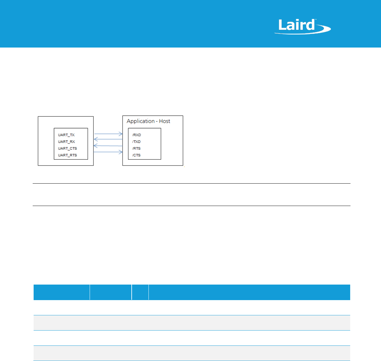
Port/TxD of the application sends data to the module’s UART_RX signal line
Port/RxD of the application receives data from the module’s UART_TX signal line
Figure 3: UART signals
Note: The BL651 serial module output is at 3.3V CMOS logic levels (tracks VCC). Level conversion must be added to
interface with an RS-232 level compliant interface.
Some serial implementations link CTS and RTS to remove the need for handshaking. We do not recommend linking CTS and
RTS other than for testing and prototyping. If these pins are linked and the host sends data at the point that the BL651 de-
asserts its RTS signal, then there is significant risk that internal receive buffers will overflow. This could lead to an internal
processor crash which would drop the connection and may require a power cycle to reset the module. We recommend that
the correct CTS/RTS handshaking protocol be adhered to for proper operation.
The BL651 module PIO pins to which the UART interface is mapped are those found on the Nordic development board as
well as the BL652 development board. You can bring out UART on any pins allowed by Nordic within the user application.
Table 13: UART interface
BL651
Signal Name
BL651
Pin Number
I/O
Comments
P0.06 / UART_Tx
19
O
P0.06 (alternative function UART_Tx) is an output, set high (in customers application via Nordic
SDK)
P0.08 / UART_Rx
17
I
P0.08 (alternative function UART_Rx) is an input, set with internal pull-up (in customers
application via Nordic SDK)
P0.05 / UART_RTS
20
O
P0.05 (alternative function UART_RTS) is an output, set low (in customers application via
Nordic SDK)
P0.07 / UART_CTS
18
I
P0.07 (alternative function UART_CTS) is an input, set with internal pull-down (in customers
application via Nordic SDK)
5.6 SPI Bus
The SPI interface is an alternate function on GPIO pins.
The module can be a master device (or slave device) that uses terminals SPI_MOSI, SPI_MISO, and SPI_CLK. SPI_CS is
implemented using any spare SIO digital output pins to allow for multi-dropping. Each multidrop SPI slave device requires a
unique and dedicated SPI_CS line.
The SPI interface enables full duplex synchronous communication between devices. It supports a 3-wire (SPI_MOSI,
SPI_MISO, SPI_SCK) bi-directional bus with fast data transfers to and from multiple slaves. Individual chip select signals are
BL651
BL651 Series
Datasheet
www.lairdtech.com/bluetooth
21
© Copyright 2018 Laird. All Rights Reserved
Americas: +1-800-492-2320
Europe: +44-1628-858-940
Hong Kong: +852 2923 0610
necessary for each of the slave devices attached to a bus, but control of these is left to the application through use of SIO
signals. I/O data is double-buffered.
The SPI peripheral supports SPI mode 0, 1, 2, and 3.
Table 14: SPI interfaces
BL651 Signal Name
BL651 Pin No
I/O
Comments
P0.23/SPI_MOSI
3
O
This interface is an alternate function.
P0.24/SPI_MISO
2
I
P0.25/SPI_CLK
38
O
Any_P0.xx/SPI_CS
4
I
SPI_CS is implemented using any spare SIO digital output pins to
allow for multi-dropping. On Laird BL652 devboard, SIO_22 (pin 4)
is used as SPI_CS.
The BL651 module PIO pins to which the SPI interface is mapped are those found on the Nordic development board as well
as the BL652 development board. You can bring out SPI on any pins allowed by Nordic within the user application.
5.7 I2C Interface
The I2C interface is an alternate function on GPIO pins.
The two-wire interface can interface a bi-directional wired-OR bus with two lines (SCL, SDA) and has master/slave topology.
Data rates of 100 kbps and 400 kbps are supported along with 250 kbps for master only. The interface is capable of clock
stretching.
An I2C interface allows multiple masters and slaves to communicate over a shared wired-OR type bus consisting of two lines
which normally sit at VCC. The BL651 module can only be configured as an I2C master or slave. The SCL is the clock line
which is always sourced by the master; and SDA is a bi-directional data line which can be driven by any device on the bus.
IMPORTANT: It is essential to remember that pull-up resistors on both SCL and SDA lines are not provided in the
module and MUST be provided external to the module.
Table 15: I2C interface
BL651 Signal Name
BL651 Pin No
I/O
Comments
P0.26/I2C_SDA
37
I/O
This interface is an alternate function on each pin
P0.27/I2C_SCL
36
I/O
The BL651 module PIO pins to which the I2C interface is mapped are those found on the Nordic development board as well
as the BL652 dev board. You can bring out I2C on any pins allowed by Nordic within the user application.
5.8 General Purpose I/O, ADC, PWM, and FREQ
5.8.1 GPIO
The 19 GPIO pins are user-configured features:
Input/output direction
Output drive strength (standard drive 0.5 mA or high drive 3 or 5 mA –depends on VDD_nRF)
Internal pull-up and pull-down resistors (13 K Ohms typical) or no pull-up/down
Wake-up from high or low-level triggers on all pins
Input buffer disconnect
BL651 Series
Datasheet
www.lairdtech.com/bluetooth
22
© Copyright 2018 Laird. All Rights Reserved
Americas: +1-800-492-2320
Europe: +44-1628-858-940
Hong Kong: +852 2923 0610
Analog input (for selected pins)
5.8.2 ADC
The ADC is an alternate function on dedicated GPIO pins.
The BL651 provides access to 8-channel 8/10/12-bit successive approximation ADC in one-shot mode. This enables sampling
up to eight external signals through a front-end MUX. The ADC has configurable input and reference pre-scaling and sample
resolution (8, 10, and 12 bit).
5.8.2.1 Analog Interface (ADC)
Table 16: Analog interface
BL651 Signal Name
BL651 Pin
No
I/
O
Comments
P0.05/UART_RTS/AIN3 –
Analog Input
20
I
This interface is an alternate function on each pin
Configurable 8-, 10-, 12-bit resolution
Configurable voltage scaling 4, 2, 1/1, 1/3, 1/3, 1/4, 1/5, 1/6
Configurable acquisition time 3 uS, 5 uS, 10 uS, 15 uS, 20 uS, 40 uS
Full scale input range (VCC)
P0.04/AIN2 – Analog Input
21
I
P0.03/AIN1 – Analog Input
22
I
P0.02/AIN0 – Analog Input
23
I
P0.31/AIN7 – Analog Input
32
I
P0.30/AIN6 – Analog Input
33
I
P0.29/AIN5 – Analog Input
34
I
P0.28/AIN4 – Analog Input
35
I
5.8.3 PWM Signal Output on SIO Pins
The PWM output is an alternate function on GPIO pins.
The PWM output signal has a frequency and duty cycle property. Frequency is adjustable (up to one MHz) and the duty cycle
can be set over a range from 0% to 100%
PWM output signal has a frequency and duty cycle property. PWM output is generated using dedicated hardware in the
chipset. There is a trade-off between PWM output frequency and resolution.
For example:
PWM output frequency of 500 kHz (2 uS) results in resolution of 1:2
PWM output frequency of 100 kHz (10 uS) results in resolution of 1:10
PWM output frequency of 10 kHz (100 uS) results in resolution of 1:100
PWM output frequency of 1 kHz (1000 uS) results in resolution of 1:1000
5.9 nRESET pin
Table 17: nRESET pin
BL651 Signal
Name
BL651
Pin
Number
I/O
Comments
nRESET
7
I
BL651 HW reset (active low). Pull the nRESET pin low for minimum 100 mS in order
for the BL651 to reset.
BL651 Series
Datasheet
www.lairdtech.com/bluetooth
23
© Copyright 2018 Laird. All Rights Reserved
Americas: +1-800-492-2320
Europe: +44-1628-858-940
Hong Kong: +852 2923 0610
5.10 Two-wire Interface SWD
You can use the two-wire (SWD) interface for application programming and debugging.
Table 18: Two-wire interface SWD
BL651 Signal Name
BL651
Pin Number
I/O
Comments
SWDIO
5
I/O
Internal pull-up resistor
SWDCLK
6
I
Internal pull-down resistor
There is also the following JTAG connector which allows on-board JTAG J-link programmer signals to be routed off the
development board. The only requirement is that you should use the following JTAG connector on the host PCB.
Table 19 shows the SWD connector MPN:
Table 19: SWD connector MPN
Reference
Part
Description and MPN (Manufacturers Part Number)
JP1
FTSH-105
Header, 1.27mm, SMD, 10-way, FTSH-105-01-L-DV Samtech
Note: Reference on the BL652 development board schematic (Figure 4) shows the DVK-BL652 development schematic
wiring only for the SWD connector and the BL651 module SWD pins.
P0.18
GND
SWDIO_BLE
VCC_BLE
P0.18
SWDCLK_BLE
GND
1
P0.23/SPI_MOSI
3
P0.17 30
P0.15 29
P0.13 28
P0.22
4
GND
27
P0.10
14 P0.09
15
P0.25/SPI_CLK 38
nRESET/P0.21
7
VDD_nRF
26
P0.16
10
P0.24/SPI_MISO
2
GND
16
SWDIO
5SWDCLK
6
P0.20
8P0.18
9
P0.14
11 P0.12
12 P0.11
13
P0.08/UART_RX
17 P0.07/UART_CTS
18 P0.06/UART_TX
19 P0.05/UART_RTS/AIN3
20 P0.04/AIN2
21 P0.03/AIN1
22 P0.02/AIN0
23 P0.01/XL2
24 P0.00/XL1
25
P0.19 31
P0.31/AIN7 32
P0.30/AIN6 33
P0.29/AIN5 34
P0.28/AIN4 35
P0.27/I2C_SCL 36
P0.26/I2C_SDA 37
GND 39
GND
GND
VCC_BLE
GND
nRESET_BLE
C9
0.1uF,16V
GND
BL651 Series
Datasheet
www.lairdtech.com/bluetooth
24
© Copyright 2018 Laird. All Rights Reserved
Americas: +1-800-492-2320
Europe: +44-1628-858-940
Hong Kong: +852 2923 0610
Figure 4: BL652 development board schematic
We recommend that you use SWD (2-wire interface) to handle customer developed BL651 module firmware upgrades. You
MUST wire out the SWD (2-wire interface) on your host design (see Figure 4, where four lines should be wired out, namely
SWDIO, SWDCLK, GND and VCC).
P0.18 is a trace output (called SWO, Serial Wire Output) and is not necessary for programming the BL651 over the SWD
interface.
nReset_BLE is not necessary for programming the BL651 over the SWD interface.
5.11 BL651 Wakeup
5.11.1 Waking Up BL651 from Host
Wake the BL651 from the host using wake-up pins (any PIO pin). You may configure the BL651’s wakeup pins in the
customers application to do any of the following:
Wake up when signal is low
Wake up when signal is high
Wake up when signal changes
5.12 Low Power Modes
The BL651 has three power modes: Run (Active), Standby Doze (SYSTEM ON IDLE), and Deep Sleep (SYSTEM OFF).
The module wakes from Standby Doze via any interrupt (such as a received character on the UART Rx line). If the module
receives a UART character from either the external UART or the radio, it wakes up.
Deep sleep is the lowest power mode. Once awakened, the system goes through a system reset.
5.13 Temperature Sensor
The on-silicon temperature sensor has a temperature range greater than or equal to the operating temperature of the
device with accuracy ±5°C. Resolution is 0.25°C .
5.14 Security/Privacy
5.14.1 AES Encryption/Decryption
Exposed via Nordic SDK functions, refer to Nordic documentation.
GND
SWDIO
VCC_IO
SWDCLK
JP1
PIN HEADER,1.27mm 2X5P
1 2
3 4
5 6
7 8
910
PIN HEADER,2.54mm 1X3P
J3
11
22
3
3
PIN HEADER,2.54mm 1X3P
J4
11
2
2
3
3
SWDCLK_BLE
nRESET_BLE
P0.18
SWDIO_BLE
BL651 Series
Datasheet
www.lairdtech.com/bluetooth
25
© Copyright 2018 Laird. All Rights Reserved
Americas: +1-800-492-2320
Europe: +44-1628-858-940
Hong Kong: +852 2923 0610
5.14.2 Readback Protection
Exposed via Nordic SDK functions, refer to Nordic documentation.
The BL651 supports readback protection capability that disallows the reading of the memory on the nRF52810 using a JTAG
interface.
5.14.3 Elliptic Curve Cryptography
Exposed via Nordic SDK functions, refer to Nordic documentation.
The BL651 offers a range of functions for generating public/private keypair, calculating a shared secret, as well as generating
an authenticated hash.
5.15 Optional External 32.768 kHz Crystal
This is not required for normal BL651 module operation. Nordic SDK examples by default assume that he external 32.768
kHz crystal is connected. The customer must modify the Nordic SDK example to reflect whether or not the external 32.768
kHz crystal is fitted.
The BL651 uses the on-chip 32.76 kHz RC oscillator (LFCLK) by default (which has an accuracy of ±500 ppm); this requires
regulator calibration (at least every eight seconds) to within ±500 ppm.
You can connect an optional external high accuracy (±20 ppm) 32.768 kHz crystal to the BL651pins, P0.01/XL2 (pin 24) and
P0.00/XL1 (pin 25) to provide improved protocol timing and to help with radio power consumption in the system standby
doze/deep sleep modes by reducing the time that the RX window needs to be open. 錯誤! 找不到參照來源。 compares the
current consumption difference between RC and crystal oscillator.
Table 20: Current consumption difference between BL651 on-chip RC 32.76 kHz oscillator and optional external crystal (32.768 kHz)
based oscillator
BL651 On-chip 32.768 kHz RC Oscillator
(±500 ppm) LFRC
Optional External Higher Accuracy
(±20 ppm) 32.768 kHz
Crystal-based Oscillator XO
Current Consumption of
32.768 kHz Block
0.6 uA
0.25 uA
Standby Doze
Current (System ON
IDLE+24k RAM
retention+RTC+LFRC)
1.5 uA
2.0 uA
Calibration
Calibration is required regularly (default eight seconds interval)
Calibration takes 16-17 ms; with DCDC used, the total charge of a
calibration event is 7.4 uC.
The average current consumed by the calibration depends on the
calibration interval and can be calculated using the following formula:
CAL_charge/CAL_interval
The lowest calibration interval (0.25 seconds) provides an average
current of (DCDC enabled):
7.4uC / 0.25s = 29.6uA
To get the 500-ppm accuracy, the BLE stack specification states that a
calibration interval of eight seconds is enough. This gives an average
current of:
7.4uC/8s = 0.93 uA
Added to the LFRC run current and Standby Doze (IDLE) base current
shown above results in a total average current of:
LFRC + CAL = 1.5 + 0.93 = 2.43uA
Not applicable
Total
2.43 uA
1.45 uA
BL651 Series
Datasheet
www.lairdtech.com/bluetooth
26
© Copyright 2018 Laird. All Rights Reserved
Americas: +1-800-492-2320
Europe: +44-1628-858-940
Hong Kong: +852 2923 0610
Summary
Low current consumption
Accuracy 500 ppm
Lowest current consumption
Needs external crystal
High accuracy (depends on the crystal, usually 20
ppm)
Table 21: Optional external 32.768 kHz crystal specification
Optional external 32.768kHz crystal
Min
Typ
Max
Crystal Frequency
-
32.768 kHz
-
Frequency tolerance requirement of BLE stack
-
-
±250 ppm
Load Capacitance
-
-
12.5 pF
Shunt Capacitance
-
-
2 pF
Equivalent series resistance
-
-
100 kOhm
Drive level
-
-
1 uW
Input capacitance on XL1 and XL2 pads
-
4 pF
-
Run current for 32.768 kHz crystal based oscillator
-
0.25 uA
-
Startup time for 32.768 kHz crystal based oscillator
-
0.25 seconds
-
Peak to peak amplitude for external low swing clock input signal
must not be outside supply rails
200 mV
-
1000 mV
Be sure to tune the load capacitors on the board design to optimize frequency accuracy (at room temperature) so it matches
that of the same crystal standalone, Drive Level (so crystal operated within safe limits) oscillation margin (Rneg is at least 3 to
5 times ESR) over the operating temperature range.
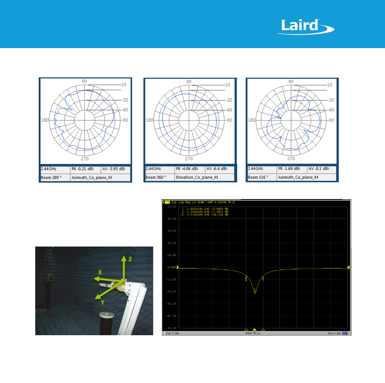
5.16 453-00005 On-board PCB Trace Antenna Characteristics
The 453-00005 on-board PCB trace monopole antenna radiated performance depends on the host PCB layout.
A Laird internal BL651 development board was used for BL651 development and antenna performance evaluation. To obtain
similar performance, follow guidelines in section PCB Layout on Host PCB for 453-00005 to allow the on-board PCB trace
antenna to radiate and reduce proximity effects due to nearby host PCB GND copper or metal covers.
Table 22: Antenna radiation performance
Unit in dBi @2.44GHz
XY-plane
XZ-plane
YZ-plane
Peak
Avg
Peak
Avg
Peak
Avg
453-00005 module on-board PCB Trace antenna
-0.21
-3.95
-1.69
-8.1
-4.06
-6.4
BL651 Series
Datasheet
www.lairdtech.com/bluetooth
27
© Copyright 2018 Laird. All Rights Reserved
Americas: +1-800-492-2320
Europe: +44-1628-858-940
Hong Kong: +852 2923 0610
◆XY-plane
Figure 5: Trace antenna performance
◆XZ-plane
◆YZ-plane
Figure 6: 453-00005 on-board PCB Trace antenna performance (Antenna Gain, efficiency and S11 (whilst 453-00005 module on DVK-
BL652-xx development board)
BL651 Series
Datasheet
www.lairdtech.com/bluetooth
28
© Copyright 2018 Laird. All Rights Reserved
Americas: +1-800-492-2320
Europe: +44-1628-858-940
Hong Kong: +852 2923 0610
6 HARDWARE INTEGRATION SUGGESTIONS
6.1 Circuit
The BL651 is easy to integrate, requiring no external components on your board apart from those which you require for
development and in your end application.
The following are suggestions for your design for the best performance and functionality.
Checklist (for Schematic):
VCC pins
External power source should be within the operating range, rise time and noise/ripple specification of the BL651. Add
decoupling capacitors for filtering the external source. Power-on reset circuitry within BL651 series module
incorporates brown-out detector, thus simplifying your power supply design. Upon application of power, the internal
power-on reset ensures that the module starts correctly.
VCC and coin-cell operation
With built-in DCDC (operating range 1.7V to 3.6V), reduces the peak current required from a coin-cell, making it easier
to use with coin-cell.
AIN (ADC) and GPIO pin IO voltage levels
BL651 GPIO voltage levels are at VCC. Ensure input voltage levels into GPIO pins are at VCC also (if VCC source is a
battery whose voltage will drop). Ensure ADC pin maximum input voltage for damage is not violated.
AIN (ADC) impedance and external voltage divider setup
If you need to measure with ADC a voltage higher than 3.6V, you can connect a high impedance voltage divider to
lower the voltage to the ADC input pin.
SWD
We recommend that use SWD (2-wire interface) to handle customer developed BL651 module firmware upgrades. You
MUST wire out the JTAG (2-wire interface) on your host design (see Figure 4, where four lines should be wired out,
namely SWDIO, SWDCLK, GND and VCC).
UART
Add connector to allow interfacing with UART via PC (UART–RS232 or UART-USB). Laird recommends flow control to
prevent UART data loss.
I2C
It is essential to remember that pull-up resistors on both I2C_SCL and I2C_SDA lines are not provided in the BL651
module and MUST be provided external to the module as per I2C standard.
SPI
Implement SPI chip select using any unused GPIO pin within customers application then SPI_CS is controlled from
customers application allowing multi-dropping.
GPIO pin direction
BL651 modules shipped from production are un-programmed. Remember to change the direction GPIO pin (in
customer developed application) if that particular pin is wired to a device that expects to be driven by the BL651 GPIO
pin configured as an output. Also, these GPIO pins if used as inputs have the internal pull-up or pull-down resistor. To
avoid floating inputs which can cause current consumption in low power modes (e.g. System ON IDLE) to drift with time;
customer can enable the PULL-UP or PULL-DOWN through their application.
Note: Internal pull-up, pull down will take current from VCC.
nRESET pin (active low)
Hardware reset. Wire out to push button or drive by host.
By default module is out of reset when power applied to VCC pins.
Optional External 32.768kHz crystal

BL651 Series
Datasheet
www.lairdtech.com/bluetooth
29
© Copyright 2018 Laird. All Rights Reserved
Americas: +1-800-492-2320
Europe: +44-1628-858-940
Hong Kong: +852 2923 0610
If the optional external 32.768kHz crystal is needed then use a crystal that meets specification. Nordic SDK examples
by default assume external 32.768kHz crystal is connected. Customer must modify Nordic SDK example to reflect if
external 32.768kHz crystal is fitted or not.
6.2 PCB Layout on Host PCB - General
Checklist (for PCB):
You MUST locate the BL651 module close to the edge of PCB (mandatory for 453-00005 for on-board PCB trace
antenna to radiate properly).
Use solid GND plane on inner layer (for best EMC and RF performance).
All module GND pins MUST be connected to host PCB GND.
Place GND vias as close to module GND pads as possible.
Unused PCB area on surface layer can flooded with copper but place GND vias regularly to connect copper flood to
inner GND plane. If GND flood copper underside the module then connect with GND vias to inner GND plane.
Route traces to avoid noise being picked up on VCC supply and AIN (analogue) and SIO (digital) traces.
Ensure no exposed copper is on the underside of the module (refer to Figure 10 land pattern of BL652 development
board).
6.3 PCB Layout on Host PCB for 453-00005
6.3.1 Antenna Keep-out on Host PCB
The 453-00005 has an integrated PCB trace antenna and its performance is sensitive to host PCB. It is critical to locate the
453-00005 on the edge of the host PCB (or corner) to allow the antenna to radiate properly. Refer to guidelines in the PCB
land pattern and antenna keep-out area for 453-00005 section. Some of those guidelines repeated below.
Ensure there is no copper in the antenna keep-out area on any layers of the host PCB. Keep all mounting hardware and
metal clear of the area to allow proper antenna radiation.
For best antenna performance, place the 453-00005 module on the edge of the host PCB, preferably the edge center.
The BL651 development board (not commercially available) has the 453-00005 module on the edge of the board
(preferably the edge center). The antenna keep-out area is defined by the BL651 development board which was used
for module development and antenna performance evaluation is shown in Figure 7, where the antenna keep-out area
is ~4.95mm wide, 25.65 mm long; with PCB dielectric (no copper) height 0.85 mm sitting under the 453-00005 PCB
trace antenna.
The 453-00005 PCB trace antenna is tuned when 453-00005 module is sitting on development board (host PCB) with
size of 120 mm x 93 mm.
A different host PCB thickness dielectric will have a small effect on antenna.
The antenna-keep-out defined in the Host PCB Land Pattern and Antenna Keep-out for 453-00005 section.
Host PCB land pattern and antenna keep-out for the BL651 applies when the 453-00005 is placed in the edge of the
host PCB, preferably the edge center. Figure 7 shows an example.
BL651 Series
Datasheet
www.lairdtech.com/bluetooth
30
© Copyright 2018 Laird. All Rights Reserved
Americas: +1-800-492-2320
Europe: +44-1628-858-940
Hong Kong: +852 2923 0610
Figure 7: Antenna keep-out area (shown in red), corner of the BL651 development board for 453-00005 module.
Antenna Keep-out Notes:
Note 1
The BL651 module is placed on the edge of the host PCB, preferably edge center of the host PCB.
Note 2
Copper cut-away on all layers in the Antenna Keep-out area under 453-00005 on host PCB.
6.3.2 Antenna Keep-out and Proximity to Metal or Plastic
Checklist (for metal /plastic enclosure):
Minimum safe distance for metals without seriously compromising the antenna (tuning) is 40 mm top/bottom and 30
mm left or right.
Metal close to the 453-00005 PCB trace monopole antenna (bottom, top, left, right, any direction) will have
degradation on the antenna performance. The amount of that degradation is entirely system dependent, meaning you
must perform some testing with your host application.
Any metal closer than 20 mm begins to significantly degrade performance (S11, gain, radiation efficiency).
It is best that you test the range with a mock-up (or actual prototype) of the product to assess effects of enclosure
height (and materials, whether metal or plastic) and host PCB size (ground plane size).
6.4 External Antenna Integration with 453-00006
Please refer to the regulatory sections for FCC, IC, CE, and Japan for details of use of BL651 (453-00006) with external
antennas in each regulatory region.
The BL651 family is designed to operate with the following external antennas (with a maximum gain of
2.0 dBi). The required antenna impedance is 50 ohms. See Table 23. External antennas improve radiation efficiency.
BL651 module
Antenna Keep-out
BL651 Series
Datasheet
www.lairdtech.com/bluetooth
31
© Copyright 2018 Laird. All Rights Reserved
Americas: +1-800-492-2320
Europe: +44-1628-858-940
Hong Kong: +852 2923 0610
Table 23: External antennas for the BL651
Manufacturer
Model
Laird
Part Number
Type
Connector
Peak Gain
2400-2480 MHz
2400-2500 MHz
Laird
NanoBlue
EBL2400A1-10MH4L
PCB Dipole
IPEX MHF4
2 dBi
Laird
FlexPIFA
001-0022
PCB Dipole
IPEX MHF4
2 dBi
Mag.Layers
EDA-8709-2G4C1-B27-CY
0600-00057
Dipole
IPEX MHF4
2 dBi
Laird
mFlexPIFA
EFA2400A3S-10MH4L
PIFA
IPEX MHF4
2 dBI
Note 1: Integral RF co-axial cable with length 100 ±5 mm and MHF4 compatible connector.
These antennas are available through Laird, Mouser, or Digikey.
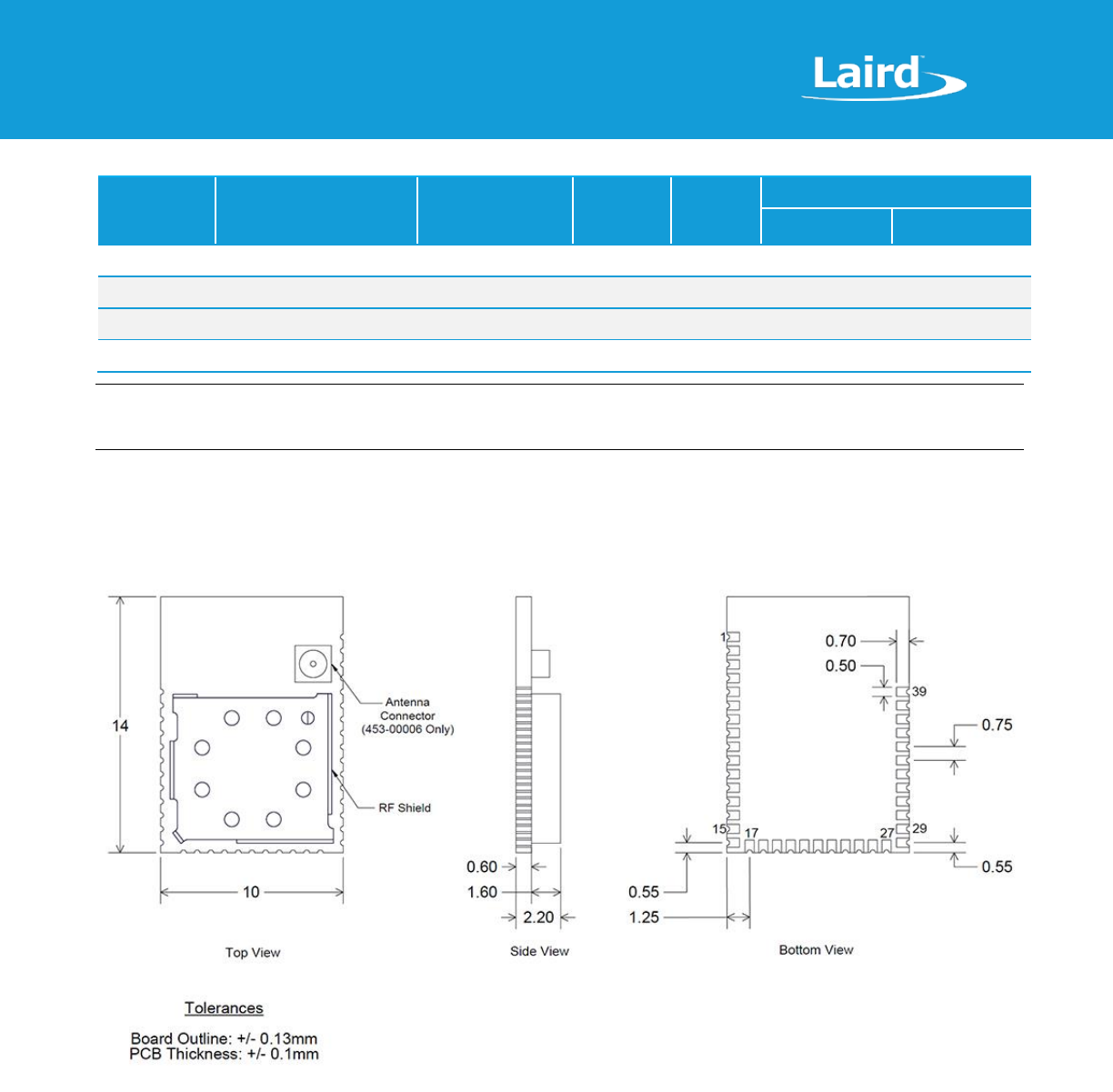
7 MECHANICAL DETAILS
7.1 BL651 Mechanical Details
Figure 8: BL651 mechanical drawings
BL651 Series
Datasheet
www.lairdtech.com/bluetooth
32
© Copyright 2018 Laird. All Rights Reserved
Americas: +1-800-492-2320
Europe: +44-1628-858-940
Hong Kong: +852 2923 0610
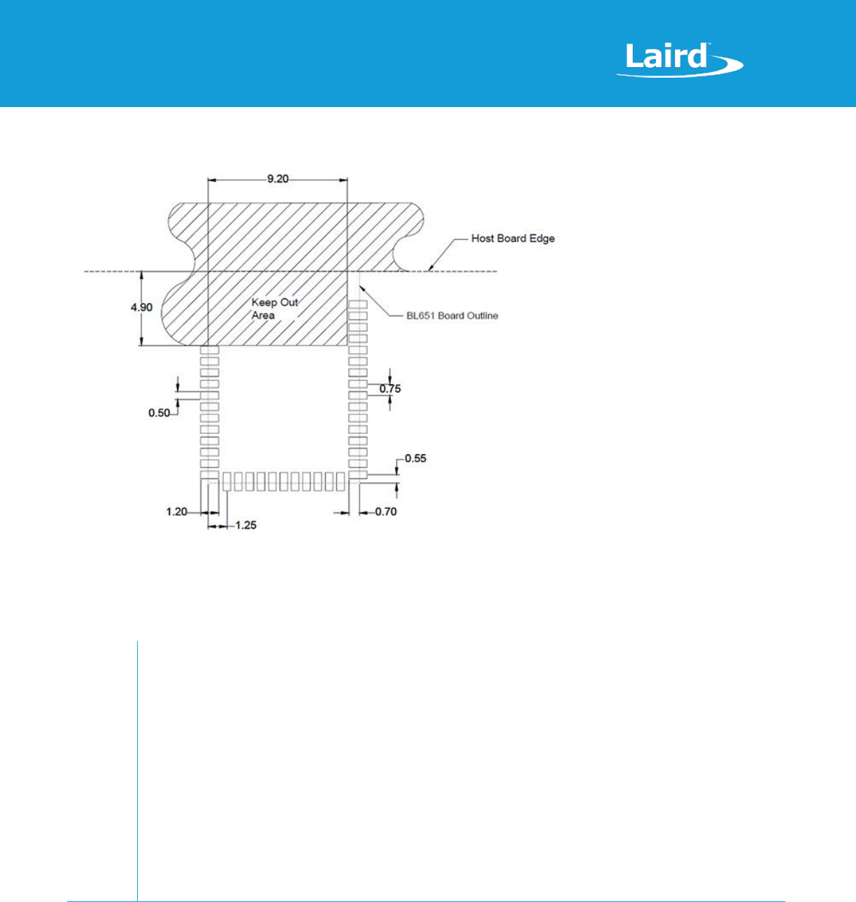
7.2 Host PCB Land Pattern and Antenna Keep-out for 453-00005
Figure 9: Land pattern and Keep-out for 453-00005
All dimensions are in millimeters (mm).
Host PCB Land Pattern and Antenna Keep-out for 453-00005 Notes:
Note 1
Ensure there is no copper in the antenna keep out area on any layers of the host PCB. Also keep all mounting
hardware or any metal clear of the area (Refer to 6.3.2) to reduce effects of proximity detuning the antenna
and to help antenna radiate properly.
Note 2
For the best on-board antenna performance, the module 453-00005 MUST be placed on the edge of the host
PCB and preferably in the edge centre of host PCB, the antenna keep out area is extended (see Note 4).
Note 3
BL651 development board has 453-00005 placed on the edge of the PCB board (and not in corner) for that the
Antenna keep out area is extended down to the corner of the development board, see the PCB Layout on Host
PCB for 453-00005 section. This was used for module development and antenna performance evaluation.
Note 4
Ensure that there is no exposed copper under the module on the host PCB.
Note 5
You may modify the PCB land pattern dimensions based on their experience and/or process capability.
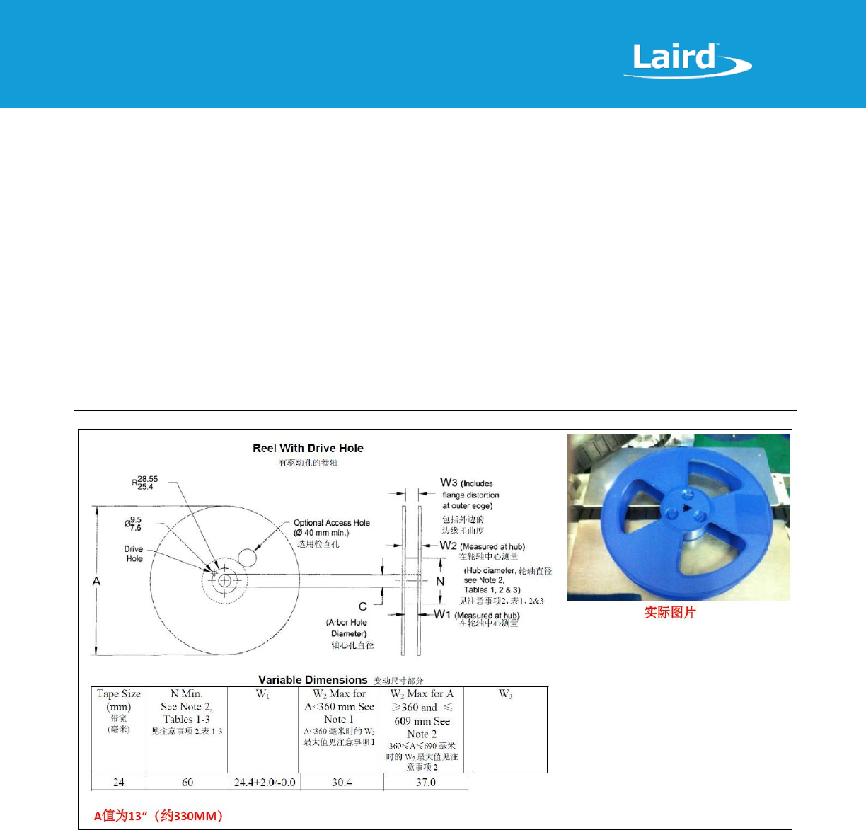
BL651 Series
Datasheet
www.lairdtech.com/bluetooth
33
© Copyright 2018 Laird. All Rights Reserved
Americas: +1-800-492-2320
Europe: +44-1628-858-940
Hong Kong: +852 2923 0610
8 APPLICATION NOTE FOR SURFACE MOUNT MODULES
8.1 Introduction
Laird Technologies’ surface mount modules are designed to conform to all major manufacturing guidelines. This Application
Note section is considered a living document and will be updated as new information is presented.
The modules are designed to meet the needs of several commercial and industrial applications. They are easy to
manufacture and conform to current automated manufacturing processes.
8.2 Shipping
8.2.1 Tape and Reel Package Information
Note: The Laird part numbers for BL651 modules – 453-00005 and 453-00006 are for Tape and Reel packaging in 1k unit
reels. The addition of a ‘C’ at the end of the part number denotes Cut Tape option.
Figure 10: Reel specifications
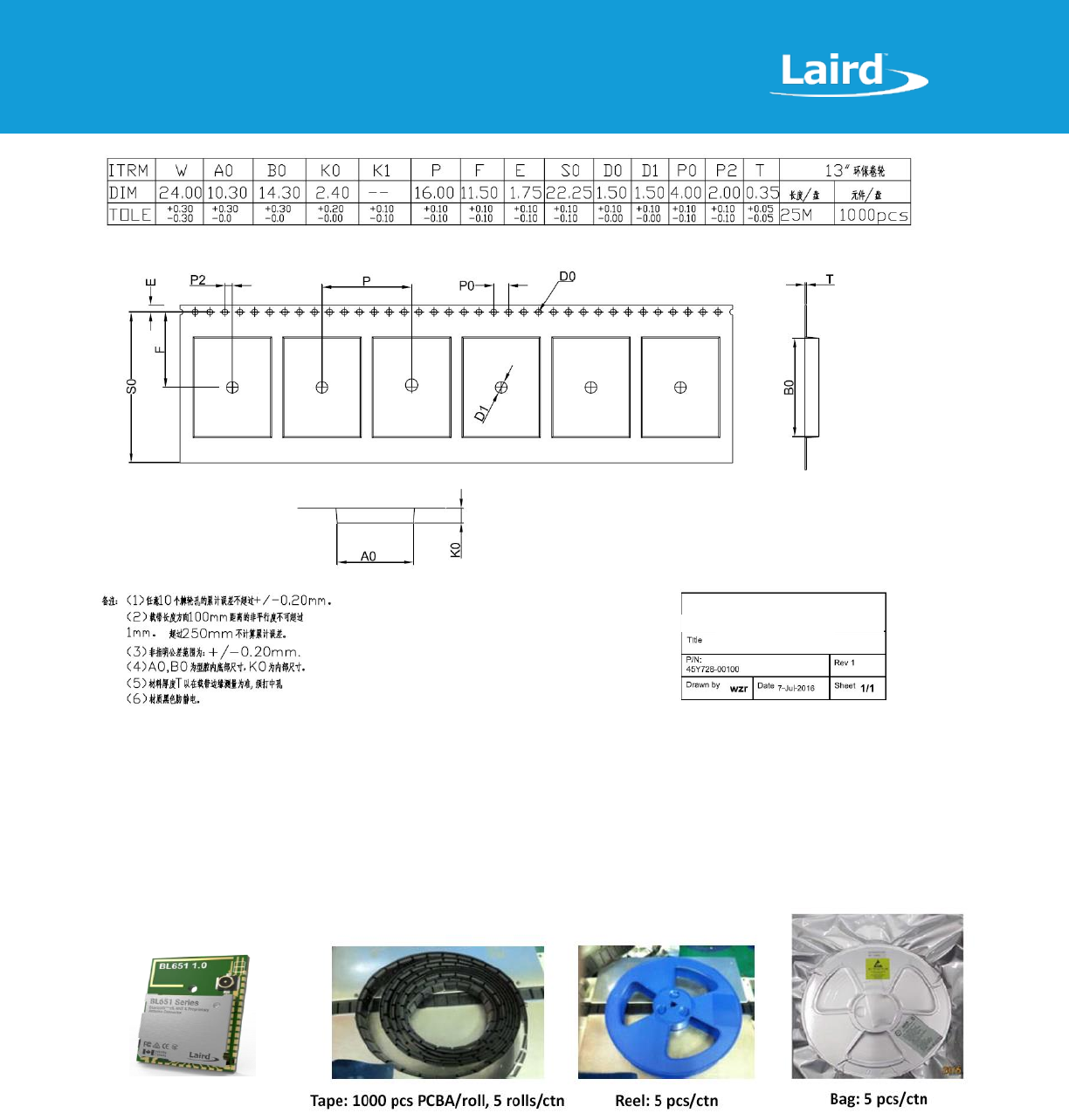
BL651 Series
Datasheet
www.lairdtech.com/bluetooth
34
© Copyright 2018 Laird. All Rights Reserved
Americas: +1-800-492-2320
Europe: +44-1628-858-940
Hong Kong: +852 2923 0610
Figure 11: Tape specifications
There are 1000 pieces of BL651 modules taped in a reel (and packaged in a pizza box) and five boxes per carton (5000
modules per carton). Reel, boxes, and carton are labeled with the appropriate labels. See Carton Contents for more
information.
8.2.2 Carton Contents
The following are the contents of the carton shipped for the BL651 modules.
PCBA: 5000 pcs/ctn
BL651 Shipping Tape
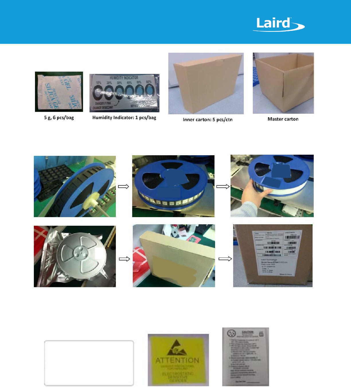
BL651 Series
Datasheet
www.lairdtech.com/bluetooth
35
© Copyright 2018 Laird. All Rights Reserved
Americas: +1-800-492-2320
Europe: +44-1628-858-940
Hong Kong: +852 2923 0610
8.2.3 Packaging Process
Figure 13: BL651 packaging process
8.2.4 Labeling
The following labels are located on the antistatic bag:
Figure 14: Antistatic bag labels
Figure 12: Carton contents for the BL651
M/N: 453-00005
QTY: 1000 PCS
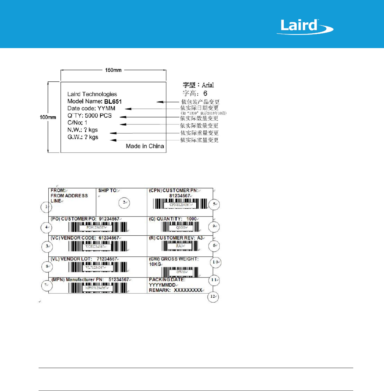
BL651 Series
Datasheet
www.lairdtech.com/bluetooth
36
© Copyright 2018 Laird. All Rights Reserved
Americas: +1-800-492-2320
Europe: +44-1628-858-940
Hong Kong: +852 2923 0610
The following package label is located on both sides of the master carton:
Figure 15: Master carton package label
The following is the packing slip label:
Figure 16: Packing slip label
8.3 Reflow Parameters
Prior to any reflow, it is important to ensure the modules were packaged to prevent moisture absorption. New packages
contain desiccate (to absorb moisture) and a humidity indicator card to display the level maintained during storage and
shipment. If directed to bake units on the card, see Table 24 and follow instructions specified by IPC/JEDEC J-STD-033. A copy
of this standard is available from the JEDEC website: http://www.jedec.org/sites/default/files/docs/jstd033b01.pdf
Note: The shipping tray cannot be heated above 65°C. If baking is required at the higher temperatures displayed in in
Table 24, the modules must be removed from the shipping tray.
Any modules not manufactured before exceeding their floor life should be re-packaged with fresh desiccate and a new
humidity indicator card. Floor life for MSL (Moisture Sensitivity Level) 4 devices is 168 hours in ambient environment
30°C/60%RH.
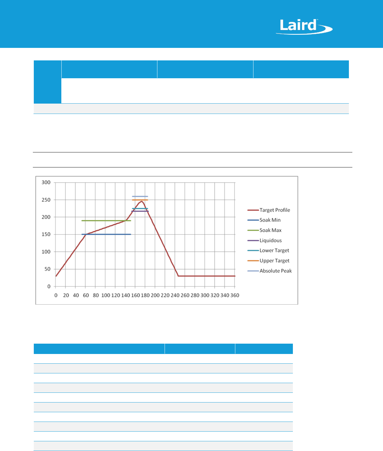
BL651 Series
Datasheet
www.lairdtech.com/bluetooth
37
© Copyright 2018 Laird. All Rights Reserved
Americas: +1-800-492-2320
Europe: +44-1628-858-940
Hong Kong: +852 2923 0610
Table 24: Recommended baking times and temperatures
MSL
125°C
Baking Temp.
90°C/≤ 5%RH
Baking Temp.
40°C/ ≤ 5%RH
Baking Temp.
Saturated
@ 30°C/85%
Floor Life Limit
+ 72 hours
@ 30°C/60%
Saturated
@ 30°C/85%
Floor Life Limit
+ 72 hours
@ 30°C/60%
Saturated
@ 30°C/85%
Floor Life Limit
+ 72 hours @
30°C/60%
3
9 hours
7 hours
33 hours
23 hours
13 days
9 days
Laird surface mount modules are designed to be easily manufactured, including reflow soldering to a PCB. Ultimately it is the
responsibility of the customer to choose the appropriate solder paste and to ensure oven temperatures during reflow meet
the requirements of the solder paste. Laird surface mount modules conform to J-STD-020D1 standards for reflow
temperatures.
Important: During reflow, modules should not be above 260° and not for more than 30 seconds.
Figure 17: Recommended reflow temperature
Temperatures should not exceed the minimums or maximums presented in Table 25.
Table 25: Recommended maximum and minimum temperatures
Specification
Value
Unit
Temperature Inc./Dec. Rate (max)
1~3
°C / Sec
Temperature Decrease rate (goal)
2-4
°C / Sec
Soak Temp Increase rate (goal)
.5 - 1
°C / Sec
Flux Soak Period (Min)
70
Sec
Flux Soak Period (Max)
120
Sec
Flux Soak Temp (Min)
150
°C
Flux Soak Temp (max)
190
°C
Time Above Liquidous (max)
70
Sec
Time Above Liquidous (min)
50
Sec
Time In Target Reflow Range (goal)
30
Sec
BL651 Series
Datasheet
www.lairdtech.com/bluetooth
38
© Copyright 2018 Laird. All Rights Reserved
Americas: +1-800-492-2320
Europe: +44-1628-858-940
Hong Kong: +852 2923 0610
Specification
Value
Unit
Time At Absolute Peak (max)
5
Sec
Liquidous Temperature (SAC305)
218
°C
Lower Target Reflow Temperature
240
°C
Upper Target Reflow Temperature
250
°C
Absolute Peak Temperature
260
°C
9 FCC AND IC REGULATORY
Model
US/FCC
Canada/IC
453-00005
SQGBL651
3147A-BL651
453-00006
SQGBL651
3147A-BL651
The BL651 Series hold full modular approvals. The OEM must follow the regulatory guidelines and warnings listed below to
inherit the modular approval.
Part #
Form Factor
Tx Outputs
Antenna
453-00005
Surface Mount
4 dBm
PCB Trace
453-00006
Surface Mount
4 dBm
IPEX MHF4
*Last two slots "XX" in Part # are used for production firmware release changes. Can be values 01-99, aa-zz
9.1 Antenna Information
The BL651 family has been designed to operate with the antennas listed below with a maximum gain of 2 dBi. The required
antenna impedance is 50 ohms.
Manufacturer
Model
Laird
Part Number
Type
Connector
Peak Gain
2400-2480 MHz
2400-2500 MHz
Laird
NanoBlue
EBL2400A1-10MH4L
PCB Dipole
IPEX MHF4
2 dBi
Laird
FlexPIFA
001-0022
PCB Dipole
IPEX MHF4
2 dBi
Mag.Layers
EDA-8709-2G4C1-B27-CY
0600-00057
Dipole
IPEX MHF4
2 dBi
Laird
mFlexPIFA
EFA2400A3S-10MH4L
PIFA
IPEX MHF4
2 dBI
Laird
BL651 PCB printed antenna
NA
Printed PCB
N/A
0 dBi
Note: The OEM is free to choose another vendor’s antenna of like type and equal or lesser gain as an antenna appearing
in the table and still maintain compliance. Reference FCC Part 15.204(c)(4) for further information on this topic.
To reduce potential radio interference to other users, the antenna type and gain should be chosen so that the
equivalent isotropic radiated power (EIRP) is not more than that permitted for successful communication.

BL651 Series
Datasheet
www.lairdtech.com/bluetooth
39
© Copyright 2018 Laird. All Rights Reserved
Americas: +1-800-492-2320
Europe: +44-1628-858-940
Hong Kong: +852 2923 0610
9.2 Power Exposure Information
Federal Communication Commission (FCC) Radiation Exposure Statement:
This EUT is in compliance with SAR for general population/uncontrolled exposure limits in ANSI/IEEE C95.1-1999 and had
been tested in accordance with the measurement methods and procedures specified in OET Bulletin 65 Supplement C.
This transceiver must not be co-located or operating in conjunction with any other antenna, transmitter, or external
amplifiers. Further testing / evaluation of the end product will be required if the OEM’s device violates any of these
requirements.
The BL651 is fully approved for mobile and portable applications.
9.3 OEM Responsibilities
WARNING: The OEM must ensure that FCC labelling requirements are met. This includes a clearly visible label on the
outside of the OEM enclosure specifying the appropriate Laird Technology FCC identifier for this product.
Contains FCC ID: SQGBL651 IC: 3147A-BL651
If the size of the end product is larger than 8x10cm, then the following FCC part 15.19 statement has to also
be available on visible on outside of device:
The enclosed device complies with Part 15 of the FCC Rules. Operation is subject to the following two
conditions: (1) This device may not cause harmful interference, and (2) This device must accept any
interference received, including interference that may cause undesired operation
Label and text information should be in a size of type large enough to be readily legible, consistent with the dimensions of
the equipment and the label. However, the type size for the text is not required to be larger than eight point.
CAUTION: The OEM should have their device which incorporates the BL651 tested by a qualified test house to verify
compliance with FCC Part 15 Subpart B limits for unintentional radiators.
CAUTION: Any changes or modifications not expressly approved by Laird Technology could void the user’s authority to
operate the equipment.
9.4 Federal Communication Commission Interference Statement
This equipment has been tested and found to comply with the limits for a Class B digital device, pursuant to Part 15 of the
FCC Rules. These limits are designed to provide reasonable protection against harmful interference in a residential
installation. This equipment generates, uses and can radiate radio frequency energy and, if not installed and used in
accordance with the instructions, may cause harmful interference to radio communications. However, there is no guarantee
that interference will not occur in a particular installation. If this equipment does cause harmful interference to radio or
television reception, which can be determined by turning the equipment off and on, the user is encouraged to try to correct
the interference by one of the following measures:
Reorient or relocate the receiving antenna.
Increase the separation between the equipment and receiver.
Connect the equipment into an outlet on a circuit different from that to which the receiver is connected.
Consult the dealer or an experienced radio/TV technician for help.
FCC Caution: Any changes or modifications not expressly approved by the party responsible for compliance could void the
user's authority to operate this equipment.

BL651 Series
Datasheet
www.lairdtech.com/bluetooth
40
© Copyright 2018 Laird. All Rights Reserved
Americas: +1-800-492-2320
Europe: +44-1628-858-940
Hong Kong: +852 2923 0610
This device complies with Part 15 of the FCC Rules. Operation is subject to the following two conditions: (1) This device may
not cause harmful interference, and (2) this device must accept any interference received, including interference that may
cause undesired operation.
IMPORTANT NOTE
FCC Radiation Exposure Statement
The product complies with the US portable RF exposure limit set forth for an uncontrolled environment and are safe for
intended operation as described in this manual. The further RF exposure reduction can be achieved if the product can be
kept as far as possible from the user body or set the device to lower output power if such function is available.
This transmitter must not be co-located or operating in conjunction with any other antenna or transmitter.
This device is intended only for OEM integrators under the following condition:
1. The transmitter module may not be co-located with any other transmitter or antenna,
As long as the condition above is met, further transmitter testing is not required. However, the OEM integrator is still
responsible for testing their end-product for any additional compliance requirements required with this module installed
IMPORTANT NOTE
In the event that these conditions cannot be met (for example certain laptop configurations or co-location with another
transmitter), then the FCC authorization is no longer considered valid and the FCC ID cannot be used on the final product. In
these circumstances, the OEM integrator is responsible for re-evaluating the end product (including the transmitter) and
obtaining a separate FCC authorization.
End Product Labeling
The final end product must be labeled in a visible area with the following: “Contains FCC ID: SQGBL651”.
Manual Information to the End User
The OEM integrator must be aware not to provide information to the end user regarding how to install or remove this RF
module in the user’s manual of the end product which integrates this module.
The end user manual shall include all required regulatory information/warning as show in this manual.
9.5 Industry Canada Statement
This device contains licence-exempt transmitter(s)/receiver(s) that comply with Innovation, Science and Economic
Development Canada’s licence-exempt RSS(s). Operation is subject to the following two conditions:
(1) This device may not cause interference
(2) This device must accept any interference, including interference that may cause undesired operation of the device
Cet appareil contient des émetteurs / récepteurs exempts de licence qui sont conformes au (x) RSS (s) exemptés de licence
d'Innovation, Sciences et Développement économique Canada. L'opération est soumise aux deux conditions suivantes:
(1) Cet appareil ne doit pas causer d'interférences
(2) Cet appareil doit accepter toute interférence, y compris les interférences pouvant provoquer un fonctionnement
indésirable de l'appareil
Radiation Exposure Statement
The product complies with the Canada portable RF exposure limit set forth for an uncontrolled environment and are safe
for intended operation as described in this manual. The further RF exposure reduction can be achieved if the product can
be kept as far as possible from the user body or set the device to lower output power if such function is available.

BL651 Series
Datasheet
www.lairdtech.com/bluetooth
41
© Copyright 2018 Laird. All Rights Reserved
Americas: +1-800-492-2320
Europe: +44-1628-858-940
Hong Kong: +852 2923 0610
Déclaration d'exposition aux radiations:
Le produit est conforme aux limites d'exposition pour les appareils portables RF pour les Etats-Unis et le Canada établies
pour un environnement non contrôlé. Le produit est sûr pour un fonctionnement tel que décrit dans ce manuel. La
réduction aux expositions RF peut être augmentée si l'appareil peut être conservé aussi loin que possible du corps de
l'utilisateur ou que le dispositif est réglé sur la puissance de sortie la plus faible si une telle fonction est disponible.
This device is intended only for OEM integrators under the following conditions:
(1) The transmitter module may not be co-located with any other transmitter or antenna.
As long as 1 condition above are met, further transmitter test will not be required. However, the OEM integrator is still
responsible for testing their end-product for any additional compliance requirements required with this module installed.
Cet appareil est conçu uniquement pour les intégrateurs OEM dans les conditions suivantes:
(1) Le module émetteur peut ne pas être coïmplanté avec un autre émetteur ou antenne.
Tant que les 1 condition ci-dessus sont remplies, des essais supplémentaires sur l'émetteur ne seront pas nécessaires.
Toutefois, l'intégrateur OEM est toujours responsable des essais sur son produit final pour toutes exigences de conformité
supplémentaires requis pour ce module installé.
IMPORTANT NOTE:
In the event that these conditions cannot be met (for example certain laptop configurations or co-location with another
transmitter), then the Canada authorization is no longer considered valid and the IC ID cannot be used on the final product.
In these circumstances, the OEM integrator will be responsible for re-evaluating the end product (including the transmitter)
and obtaining a separate Canada authorization.
NOTE IMPORTANTE:
Dans le cas où ces conditions ne peuvent être satisfaites (par exemple pour certaines configurations d'ordinateur portable
ou de certaines co-localisation avec un autre émetteur), l'autorisation du Canada n'est plus considéré comme valide et l'ID
IC ne peut pas être utilisé sur le produit final. Dans ces circonstances, l'intégrateur OEM sera chargé de réévaluer le produit
final (y compris l'émetteur) et l'obtention d'une autorisation distincte au Canada.
End Product Labeling
The final end product must be labeled in a visible area with the following: “Contains IC: 3147A-BL651”.
Plaque signalétique du produit final
Le produit final doit être étiqueté dans un endroit visible avec l'inscription suivante: "Contient des IC: 3147A-BL651".
Manual Information to the End User
The OEM integrator has to be aware not to provide information to the end user regarding how to install or remove this RF
module in the user’s manual of the end product which integrates this module.
The end user manual shall include all required regulatory information/warning as show in this manual.
Manuel d'information à l'utilisateur final
L'intégrateur OEM doit être conscient de ne pas fournir des informations à l'utilisateur final quant à la façon d'installer ou
de supprimer ce module RF dans le manuel de l'utilisateur du produit final qui intègre ce module.
Le manuel de l'utilisateur final doit inclure toutes les informations réglementaires requises et avertissements comme
indiqué dans ce manuel.
BL651 Series
Datasheet
www.lairdtech.com/bluetooth
42
© Copyright 2018 Laird. All Rights Reserved
Americas: +1-800-492-2320
Europe: +44-1628-858-940
Hong Kong: +852 2923 0610
10 JAPAN (MIC) REGULATORY
The BL651 is approved for use in the Japanese market. The part numbers listed below hold WW type certification. Refer to
ARIB-STD-T66 for further guidance on OEM’s responsibilities.
Model
Certificate Number
Antenna
453-00005
201-180356
PCB Trace
453-00006
201-180356
IPEX MHF4
10.1 Antenna Information
The BL651 was tested with antennas listed below. The OEM can choose a different manufacturers antenna but must make
sure it is of same type and that the gain is lesser than or equal to the antenna that is approved for use.
Manufacturer
Model
Laird
Part Number
Type
Connector
Peak Gain
2400-2480
MHz
2400-2500 MHz
Laird
NanoBlue
EBL2400A1-10MH4L
PCB Dipole
IPEX MHF4
2 dBi
Laird
FlexPIFA
001-0022
PCB Dipole
IPEX MHF4
2 dBi
Mag.Layers
EDA-8709-2G4C1-B27-CY
0600-00057
Dipole
IPEX MHF4
2 dBi
Laird
mFlexPIFA
EFA2400A3S-10MH4L
PIFA
IPEX MHF4
2 dBI
Laird
BL654-SA PCB printed antenna
NA
Printed PCB
N/A
0 dBi
11 CE REGULATORY
The BL651 series have been tested for compliance with relevant standards for the EU market. The 453-00006 module was
tested with a 2 dBi antenna. The OEM can operate the 453-00006 module with any other type of antenna but must ensure
that the gain does not exceed 2 dBi to maintain the Laird approval.
The OEM should consult with a qualified test house before entering their device into an EU member country to make sure all
regulatory requirements have been met for their complete device.
Reference the Declaration of Conformities listed below for a full list of the standards that the modules were tested to. Test
reports are available upon request.
11.1 Antenna Information
The antennas listed below were tested for use with the BL651. For CE mark countries, the OEM is free to use any
manufacturer’s antenna and type of antenna if the gain is less than or equal to the highest gain approved for use (2 dBi).
Contact a Laird representative for more information regarding adding antennas.
Manufacturer
Model
Laird
Part Number
Type
Connector
Peak Gain
2400-2480
MHz
2400-2500 MHz
Laird
NanoBlue
EBL2400A1-10MH4L
PCB Dipole
IPEX MHF4
2 dBi
Laird
FlexPIFA
001-0022
PCB Dipole
IPEX MHF4
2 dBi
Mag.Layers
EDA-8709-2G4C1-B27-CY
0600-00057
Dipole
IPEX MHF4
2 dBi
Laird
mFlexPIFA
EFA2400A3S-10MH4L
PIFA
IPEX MHF4
2 dBI
Laird
BL654-SA PCB printed antenna
NA
Printed PCB
N/A
0 dBi
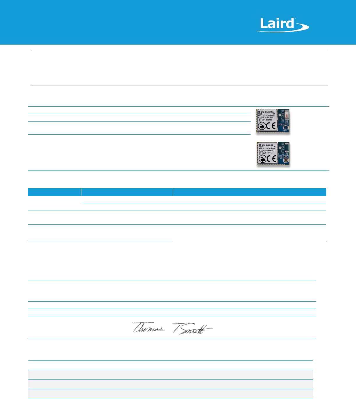
BL651 Series
Datasheet
www.lairdtech.com/bluetooth
43
© Copyright 2018 Laird. All Rights Reserved
Americas: +1-800-492-2320
Europe: +44-1628-858-940
Hong Kong: +852 2923 0610
Note: The BL651 module internal BLE chipset IC pins are rated 4 kV (ESD HBM). ESD can find its way through the
external JTAG connector (if used on the customer’s design), if discharge is applied directly. Customer should
ensure adequate protection against ESD on their end product design (using the BL651 module) to meet relevant
ESD standard (for CE, this is EN301-489).
11.2 EU Declarations of Conformity
Manufacturer
Laird
Products
453-00005, 453-00006
Product Description
Bluetooth v5.0 Module Series
EU Directives
2014/53/EU – Radio Equipment Directive (RED)
Reference standards used for presumption of conformity:
Article Number
Requirement
Reference standard(s)
3.1a
Low voltage equipment safety
EN 60950-1:2006 +A11:2009 +A1:2010 +A12:2011 +A2:2013
RF Exposure
EN 62311:2008
3.1b
Protection requirements –
Electromagnetic compatibility
EN 301 489-1 v2.2.0 (2017-03)
EN 301 489-17 v3.2.0 (2017-03)
3.2
Means of the efficient use of the
radio frequency spectrum (ERM)
EN 300 328 v2.1.1 (2016-11)
Wide-band transmission
systems
Declaration:
We, Laird, declare under our sole responsibility that the essential radio test suites have been carried out and that the above
product to which this declaration relates is in conformity with all the applicable essential requirements of Article 3 of the EU
Radio Equipment Directive 2014/53/EU, when used for its intended purpose.
Place of Issue:
Laird
W66N220 Commerce Court, Cedarburg, WI 53012 USA
tel: +1-262-375-4400 fax: +1-262-364-2649
Date of Issue:
July 2018
Name of Authorized Person:
Thomas T Smith, Director of EMC Compliance
Signature of Authorized Person:
12 ORDERING INFORMATION
453-00005
BL651 Series - Bluetooth v5 Module, Int. Antenna (Nordic nRF52810) – Tape & Reel
453-00006
BL651 Series - Bluetooth v5 Module, Ext. Antenna (Nordic nRF52810) – Tape & Reel
453-00005C
BL651 Series - Bluetooth v5 Module, Int. Antenna (Nordic nRF52810)– Cut Tape
453-00006C
BL651 Series - Bluetooth v5 Module, Ext. Antenna (Nordic nRF52810)– Cut Tape
BL651 Series
Datasheet
www.lairdtech.com/bluetooth
44
© Copyright 2018 Laird. All Rights Reserved
Americas: +1-800-492-2320
Europe: +44-1628-858-940
Hong Kong: +852 2923 0610
13 BLUETOOTH SIG QUALIFICATION
13.1 Overview
The BL651 series is listed on the Bluetooth SIG website as a qualified End Product.
Design
Name
Owner
Declaration ID
QD ID
Link to listing on the SIG website
BL651
Series
Laird
Technologies
TBC
TBC
TBC
It is a mandatory requirement of the Bluetooth Special Interest Group (SIG) that every product implementing Bluetooth
technology has a Declaration ID. Every Bluetooth design is required to go through the qualification process, even when
referencing a Bluetooth Design that already has its own Declaration ID. The Qualification Process requires each company to
registered as a member of the Bluetooth SIG – www.bluetooth.org
The following link provides a link to the Bluetooth Registration page: https://www.bluetooth.org/login/register/
For each Bluetooth Design, it is necessary to purchase a Declaration ID. This can be done before starting the new
qualification, either through invoicing or credit card payment. The fees for the Declaration ID will depend on your
membership status, please refer to the following webpage:
https://www.bluetooth.org/en-us/test-qualification/qualification-overview/fees
For a detailed procedure of how to obtain a new Declaration ID for your design, please refer to the following SIG document:
https://www.bluetooth.org/DocMan/handlers/DownloadDoc.ashx?doc_id=283698&vId=317486
13.2 Qualification Steps When Referencing a Laird End Product Design
To start a listing, go to: https://www.bluetooth.org/tpg/QLI_SDoc.cfm
In step 1, select the option, Reference a Qualified Design and enter TBC in the End Product table entry. You can then select
your pre-paid Declaration ID from the drop down menu or go to the Purchase Declaration ID page, (please note that unless
the Declaration ID is pre-paid or purchased with a credit card, it will not be possible to proceed until the SIG invoice is paid.
Once all the relevant sections of step 1 are finished, complete steps 2, 3, and 4 as described in the help document. Your new
Design will be listed on the SIG website and you can print your Certificate and DoC.
For further information, please refer to the following training material:
https://www.bluetooth.org/en-us/test-qualification/qualification-overview/listing-process-updates
Note:
13.3 Qualification Steps When Deviating from a Laird End Product Design
If you wish to deviate from the standard End Product design listed under D031950, the qualification process follows the
Traditional Project route, creating a new design. When creating a new design, it is necessary to complete the full
qualification listing process and also maintain a compliance folder for the new design.
The BL651 design under D031950 incorporates the following components:
Listing
reference
Design
Name
Core
Spec
Version
BL651 Series
Datasheet
www.lairdtech.com/bluetooth
45
© Copyright 2018 Laird. All Rights Reserved
Americas: +1-800-492-2320
Europe: +44-1628-858-940
Hong Kong: +852 2923 0610
In the future, Nordic may list updated versions of these components and it is possible to use them in your new design. Please
check with Nordic to make sure these software components are compatible with the nRF52 hardware (D029601).
If your design is based on un-modified BL651 hardware it is possible use the following process;
2. Reference the existing RF-PHY test report from the BL651 listing.
3. Combine the relevant Nordic Link Layer (LL) – check QDID with Nordic.
4. Combine in a Host Component (covering L2CAP, GAP, ATT, GATT, SM) - check QDID with Nordic.
5. Test any standard SIG profiles that are supported in the design (customs profiles are exempt).
Figure 18: Scope of the qualification for an End Product Design
The first step is to generate a project on the TPG (Test Plan Generator) system. This determines which test cases apply to
demonstrate compliance with the Bluetooth Test Specifications. If you are combining pre-tested and qualified components
in your design and they are within their three-year listing period, you are not required to re-test those layers covered by
these components.
If the design incorporates any standard SIG LE profiles (such as Heart Rate Profile), it is necessary to test these profiles using
PTS or other tools where permitted; the results are added to the compliance folder.
You are required to upload your test declaration and test reports (where applicable) and then complete the final listing steps
on the SIG website. Remember to purchase your Declaration ID before you start the qualification process, as it’s impossible
to complete the listing without it.
14 ADDITIONAL ASSISTANCE
Please contact your local sales representative or our support team for further assistance:
Laird Technologies Connectivity Products Business Unit
Support Centre: http://ews-support.lairdtech.com
Email: wireless.support@lairdtech.com
End
Product
Laird RF-PHY
Nordic LL
Host
Layers
Profiles

BL651 Series
Datasheet
www.lairdtech.com/bluetooth
46
© Copyright 2018 Laird. All Rights Reserved
Americas: +1-800-492-2320
Europe: +44-1628-858-940
Hong Kong: +852 2923 0610
Phone: Americas: +1-800-492-2320
Europe: +44-1628-858-940
Hong Kong: +852 2923 0610
Web: http://www.lairdtech.com/bluetooth
© Copyright 2018 Laird. All Rights Reserved. Patent pending. Any information furnished by Laird and its agents is believed to be accurate and reliable. All
specifications are subject to change without notice. Responsibility for the use and application of Laird materials or products rests with the end user since
Laird and its agents cannot be aware of all potential uses. Laird makes no warranties as to non-infringement nor as to the fitness, merchantability, or
sustainability of any Laird materials or products for any specific or general uses. Laird, Laird Technologies, Inc., or any of its affiliates or agents shall not be
liable for incidental or consequential damages of any kind. All Laird products are sold pursuant to the Laird Terms and Conditions of Sale in effect from time
to time, a copy of which will be furnished upon request. When used as a tradename herein, Laird means Laird PLC or one or more subsidiaries of Laird PLC.
Laird™, Laird Technologies™, corresponding logos, and other marks are trademarks or registered trademarks of Laird. Other marks may be the property of
third parties. Nothing herein provides a license under any Laird or any third party intellectual property right.