Laird Connectivity BT850 Bluetooth 4.2 Dual Mode USB HCI Module, Bluetooth 4.2 Dual Mode UART HCI Module User Manual CS GUIDE BT860 Certs
Laird Technologies Bluetooth 4.2 Dual Mode USB HCI Module, Bluetooth 4.2 Dual Mode UART HCI Module CS GUIDE BT860 Certs
Contents
- 1. Users Manual-1
- 2. Users Manual-2
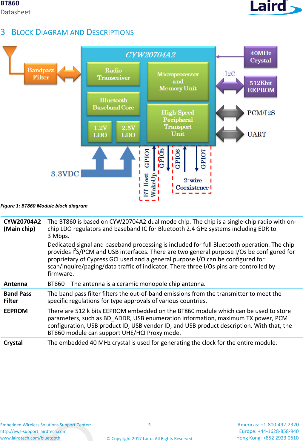
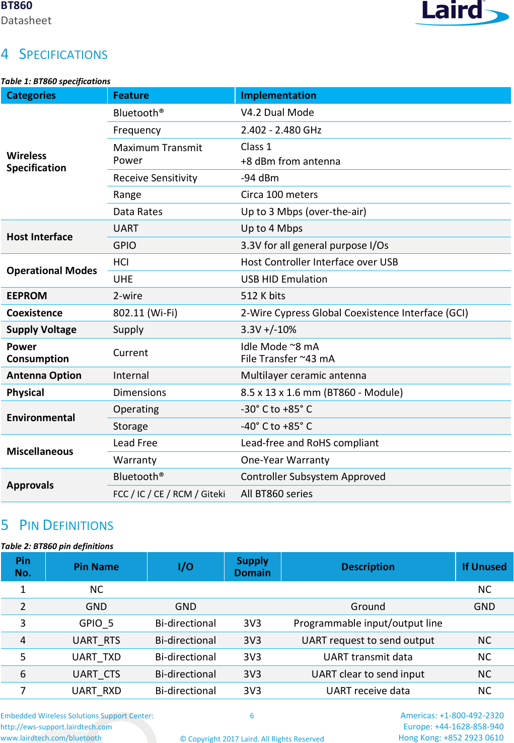
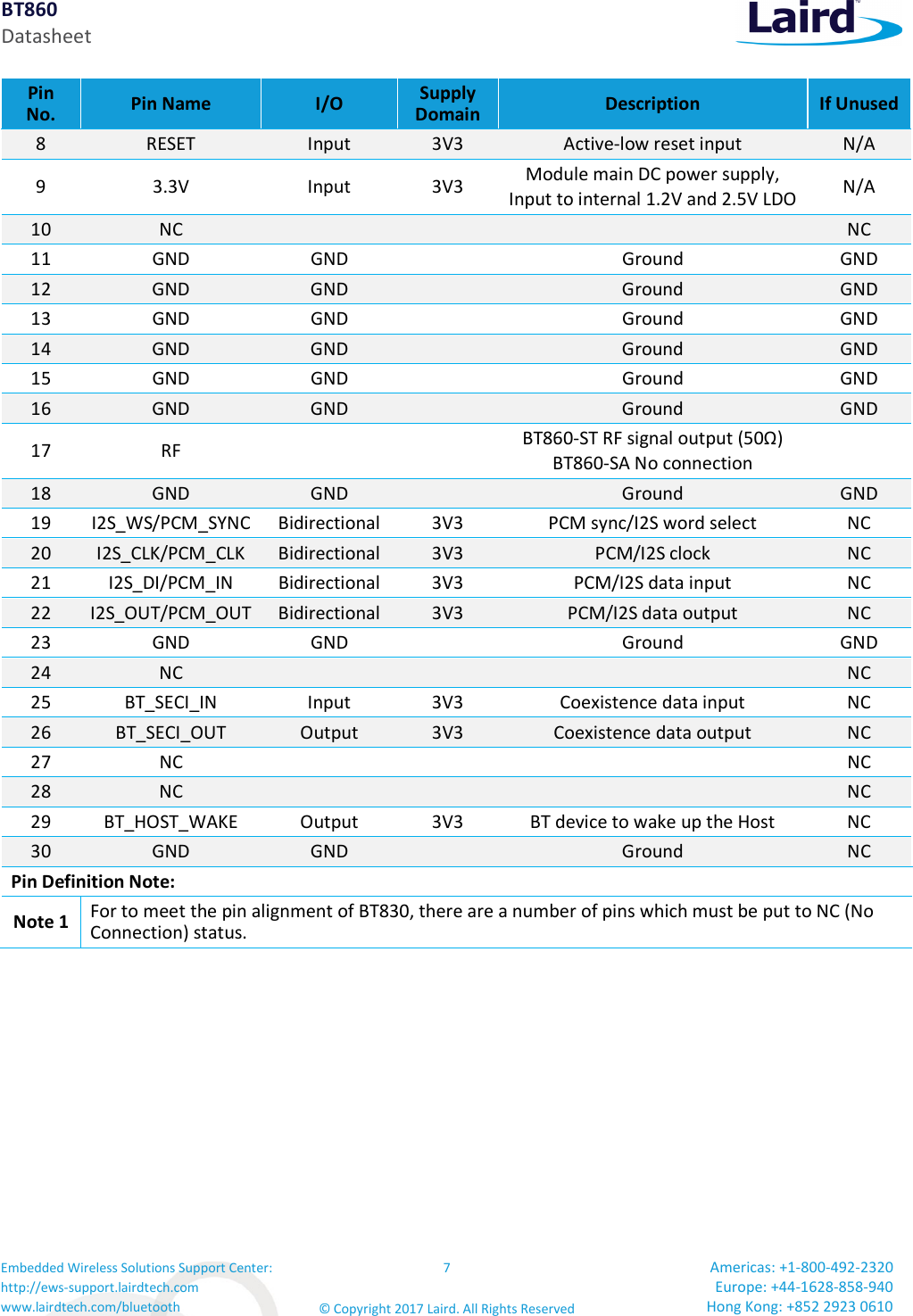
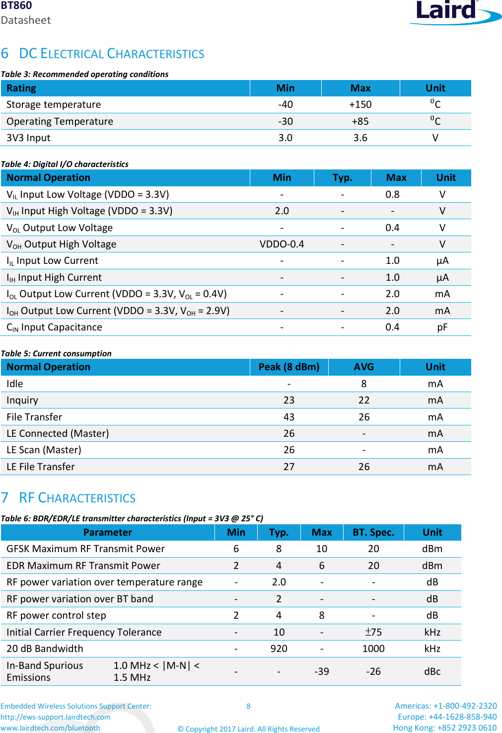
Users Manual-2