Laird Connectivity BT850 Bluetooth 4.2 Dual Mode USB HCI Module, Bluetooth 4.2 Dual Mode UART HCI Module User Manual CS GUIDE BT860 Certs
Laird Technologies Bluetooth 4.2 Dual Mode USB HCI Module, Bluetooth 4.2 Dual Mode UART HCI Module CS GUIDE BT860 Certs
Contents
- 1. Users Manual-1
- 2. Users Manual-2
Users Manual-2

A
Datasheet
BT860
Bluetooth v4.2 Dual-Mode UART HCI Module
Version 1.0

BT860
Datasheet
Embedded Wireless Solutions Support Center:
http://ews-support.lairdtech.com
www.lairdtech.com/bluetooth
2
© Copyright 2017 Laird. All Rights Reserved
Americas: +1-800-492-2320
Europe: +44-1628-858-940
Hong Kong: +852 2923 0610
R
EVISION
H
ISTORY
Version Date Notes Approver
1.0 04 Dec. 2017 Initial Release Jacky Kuo

BT860
Datasheet
Embedded Wireless Solutions Support Center:
http://ews-support.lairdtech.com
www.lairdtech.com/bluetooth
3
© Copyright 2017 Laird. All Rights Reserved
Americas: +1-800-492-2320
Europe: +44-1628-858-940
Hong Kong: +852 2923 0610
C
ONTENTS
1 Scope ............................................................................................................................................................. 4
2 Operational Description ........................................................................................................................... 4
3 Block Diagram and Descriptions ............................................................................................................... 5
4 Specifications ........................................................................................................................................... 6
5 Pin Definitions .......................................................................................................................................... 6
6 DC Electrical Characteristics ..................................................................................................................... 8
7 RF Characteristics ..................................................................................................................................... 8
8 Interface .................................................................................................................................................. 9
8.1. Global Coexistence Interface .................................................................................................................... 9
8.2. UART Interface ....................................................................................................................................... 10
8.2.1. Simultaneous UART Transport and Bridging ........................................................................................... 10
8.3. PCM Interface ........................................................................................................................................ 11
8.3.1. Slot Mapping .......................................................................................................................................... 11
8.3.2. Frame Synchronization ........................................................................................................................... 12
8.3.3.
Data Formatting
....................................................................................................................................... 15
8.3.4. Wideband Speech Support ..................................................................................................................... 16
8.3.5.
Multiplexed Bluetooth Over PCM
................................................................................................................ 16
8.3.6. Burst PCM Mode .................................................................................................................................... 16
8.4. I
2
S Interface............................................................................................................................................ 18
8.5. BSC (Cypress Serial Control) Master Interface ......................................................................................... 20
9 Antenna Performance ............................................................................................................................ 21
10 Mechanical Dimensions and Land Pattern .............................................................................................. 23
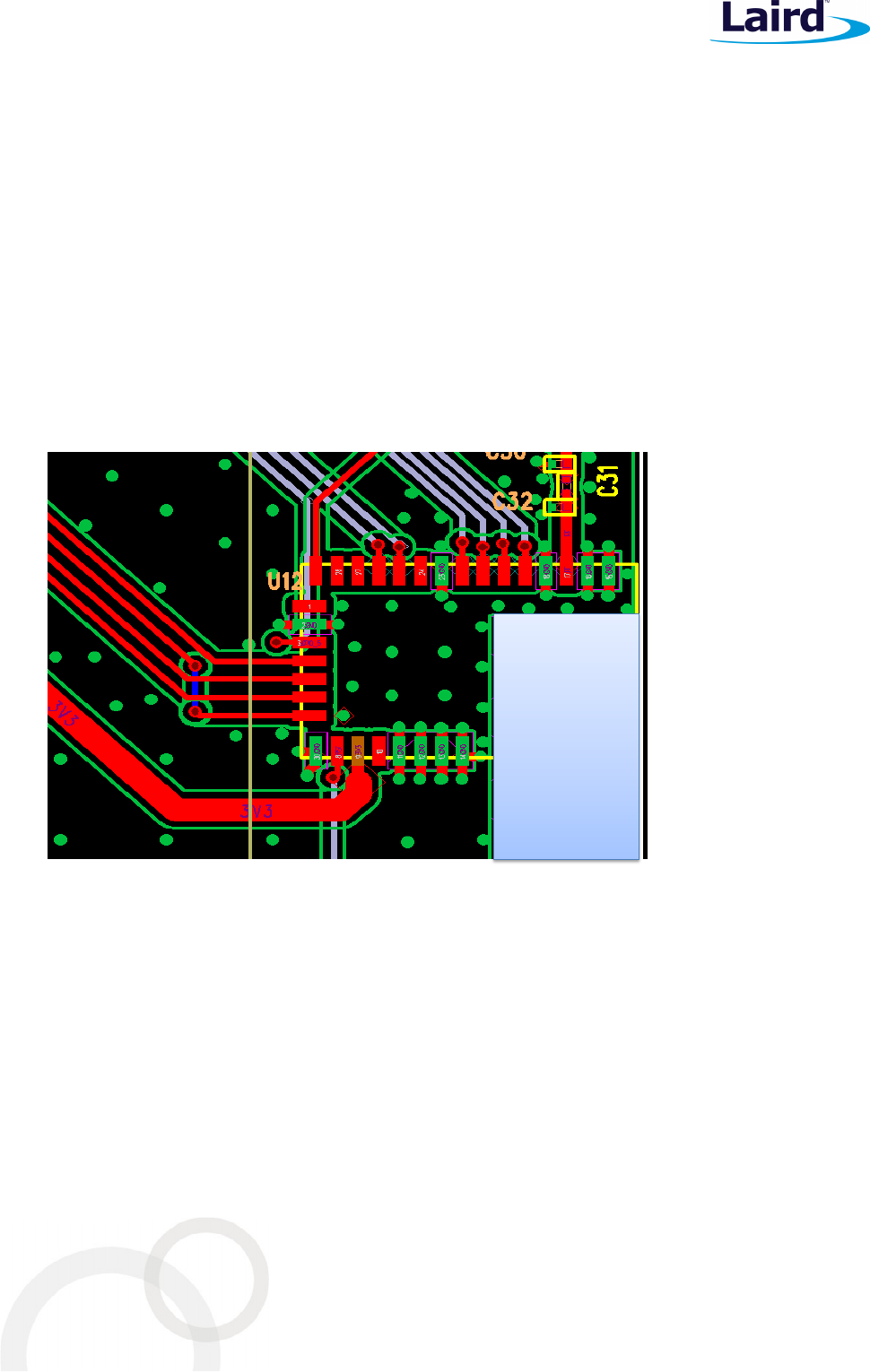
11 Implementation Note ............................................................................................................................. 24
11.1. PCB Layout on Host PCB ......................................................................................................................... 24
12 Application Note for Surface Mount Modules ........................................................................................ 25
12.1. Introduction ........................................................................................................................................... 25
12.2. Shipping ................................................................................................................................................. 25
12.3. Reflow Parameters ................................................................................................................................. 27
13 Japan (MIC) Regulatory .......................................................................................................................... 28
14 FCC Regulatory ....................................................................................................................................... 29
15 Industry Canada Regulatory ................................................................................................................... 31
16 European Union Regulatory ................................................................................................................... 32
17 Ordering Information ............................................................................................................................. 33
18 Bluetooth SIG Approvals......................................................................................................................... 34
18.1. Application Note: Subsystem Combinations ........................................................................................... 34
19 Additional Assistance ............................................................................................................................. 35
BT860
Datasheet
Embedded Wireless Solutions Support Center:
http://ews-support.lairdtech.com
www.lairdtech.com/bluetooth
4
© Copyright 2017 Laird. All Rights Reserved
Americas: +1-800-492-2320
Europe: +44-1628-858-940
Hong Kong: +852 2923 0610
1
S
COPE
This document describes key hardware aspects of the Laird BT860 Bluetooth HCI module. This document is
intended to assist device manufacturers and related parties with the integration of this module into their host
devices. Data in this document are drawn from a number of sources including data sheets for the CYW20704A2.
Because the BT860 is currently in development stage, this document is preliminary and the information in this
document is subject to change. Please contact Laird Technologies or visit the Laird website at
www.Lairdtech.com to obtain the most recent version of this document.
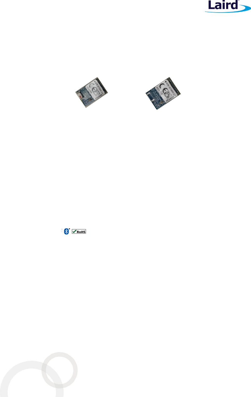
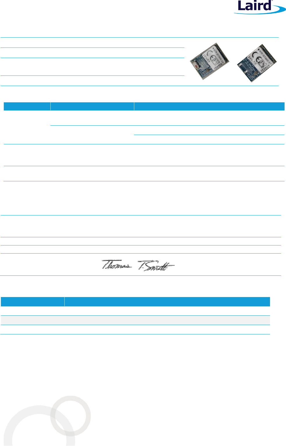
BT860-SA module
BT860-ST module
2 O
PERATIONAL
D
ESCRIPTION
The BT86x series of UART HCI modules leverage the Cypress CYW20704 A2 chipset to provide exceptionally low
power consumption with outstanding range for OEMs needing both Classic Bluetooth and Bluetooth Low Energy
support. The Bluetooth v4.2 core specification shortens your development time and provides enhanced
throughput, security and privacy.
The BT860 modules are ideal when designers need both performance and minimum size. For maximum
flexibility in integration, they support a host UART interface, I
2
S and PCM audio interfaces, GPIO, and
Cypress’GCI coexistence (2-Wire). The modules provide excellent RF performance and identical footprint options
for integrated antenna or an external antenna via a trace pin.
These modules present a Bluetooth standard HCI interface with support for Linux / Android and Embedded
Bluetooth software stacks for operating system backed devices. Additionally, Laird has partnered with Searan
for support of their ultra small, flexible ‘dotstack’ platform for embedded Cortex M3 and M4 implementations.
Features and Benefits
Application Areas
Bluetooth v4.
2
-
Dual mode (Classic Bluetooth and BLE)
Compact footprint
2-wire Cypress Global Coexistence Interface (GCI)
High antenna radiation gain and efficiency
Good interference rejection for multi-com system (GSM/WCDMA)
Class 1 output – 8 dBm
USB, I
2
S, and PCM
Industrial Temperature Range
512 k EEPROM support
Bluetooth Controller subsystem
FCC, IC, CE, RCM and Giteki approvals
Medical
devices
ePOS terminals
Barcode scanners
Industrial Cable Replacement
M2M Connectivity
Automotive Diagnostic
Equipment
Personal Digital Assistants (PDA)
Bluetooth HID device (keyboard,
mouse, joystick)
BT860
Datasheet
Embedded Wireless Solutions Support Center:
http://ews-support.lairdtech.com
www.lairdtech.com/bluetooth
5
© Copyright 2017 Laird. All Rights Reserved
Americas: +1-800-492-2320
Europe: +44-1628-858-940
Hong Kong: +852 2923 0610
3 B
LOCK
D
IAGRAM AND
D
ESCRIPTIONS
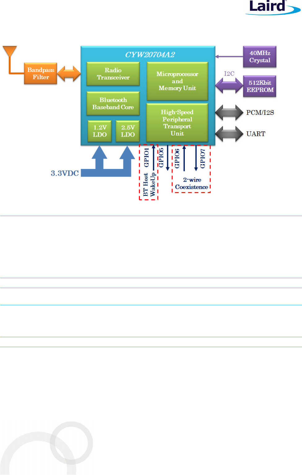
Figure 1: BT860 Module block diagram
CYW20704A2
(Main chip)
The BT860 is based on CYW20704A2 dual mode chip. The chip is a single-chip radio with on-
chip LDO regulators and baseband IC for Bluetooth 2.4 GHz systems including EDR to
3 Mbps.
Dedicated signal and baseband processing is included for full Bluetooth operation. The chip
provides I
2
S/PCM and USB interfaces. There are two general purpose I/Os be configured for
proprietary of Cypress GCI used and a general purpose I/O can be configured for
scan/inquire/paging/data traffic of indicator. There three I/Os pins are controlled by
firmware.
Antenna BT860 – The antenna is a ceramic monopole chip antenna.
Band Pass
Filter
The band pass filter filters the out-of-band emissions from the transmitter to meet the
specific regulations for type approvals of various countries.
EEPROM There are 512 k bits EEPROM embedded on the BT860 module which can be used to store
parameters, such as BD_ADDR, USB enumeration information, maximum TX power, PCM
configuration, USB product ID, USB vendor ID, and USB product description. With that, the
BT860 module can support UHE/HCI Proxy mode.
Crystal The embedded 40 MHz crystal is used for generating the clock for the entire module.

BT860
Datasheet
Embedded Wireless Solutions Support Center:
http://ews-support.lairdtech.com
www.lairdtech.com/bluetooth
6
© Copyright 2017 Laird. All Rights Reserved
Americas: +1-800-492-2320
Europe: +44-1628-858-940
Hong Kong: +852 2923 0610
4 S
PECIFICATIONS
Table 1: BT860 specifications
Categories Feature Implementation
Wireless
Specification
Bluetooth® V4.2 Dual Mode
Frequency 2.402 - 2.480 GHz
Maximum Transmit
Power
Class 1
+8 dBm from antenna
Receive Sensitivity -94 dBm
Range Circa 100 meters
Data Rates Up to 3 Mbps (over-the-air)
Host Interface UART Up to 4 Mbps
GPIO 3.3V for all general purpose I/Os
Operational Modes HCI Host Controller Interface over USB
UHE USB HID Emulation
EEPROM 2-wire 512 K bits
Coexistence 802.11 (Wi-Fi) 2-Wire Cypress Global Coexistence Interface (GCI)
Supply Voltage Supply 3.3V +/-10%
Power
Consumption Current Idle Mode ~8 mA
File Transfer ~43 mA
Antenna Option Internal Multilayer ceramic antenna
Physical Dimensions 8.5 x 13 x 1.6 mm (BT860 - Module)
Environmental Operating -30° C to +85° C
Storage -40° C to +85° C
Miscellaneous Lead Free Lead-free and RoHS compliant
Warranty One-Year Warranty
Approvals Bluetooth® Controller Subsystem Approved
FCC / IC / CE / RCM / Giteki
All BT860 series
5 P
IN
D
EFINITIONS
Table 2: BT860 pin definitions
Pin
No. Pin Name I/O Supply
Domain Description If Unused
1 NC NC
2 GND GND Ground GND
3 GPIO_5 Bi-directional
3V3 Programmable input/output line
4 UART_RTS Bi-directional
3V3 UART request to send output NC
5 UART_TXD Bi-directional
3V3 UART transmit data NC
6 UART_CTS Bi-directional
3V3 UART clear to send input NC
7 UART_RXD Bi-directional
3V3 UART receive data NC

BT860
Datasheet
Embedded Wireless Solutions Support Center:
http://ews-support.lairdtech.com
www.lairdtech.com/bluetooth
7
© Copyright 2017 Laird. All Rights Reserved
Americas: +1-800-492-2320
Europe: +44-1628-858-940
Hong Kong: +852 2923 0610
Pin
No. Pin Name I/O Supply
Domain Description If Unused
8 RESET Input 3V3 Active-low reset input N/A
9 3.3V Input 3V3 Module main DC power supply,
Input to internal 1.2V and 2.5V LDO
N/A
10 NC NC
11 GND GND Ground GND
12 GND GND Ground GND
13 GND GND Ground GND
14 GND GND Ground GND
15 GND GND Ground GND
16 GND GND Ground GND
17 RF BT860-ST RF signal output (50Ω)
BT860-SA No connection
18 GND GND Ground GND
19 I2S_WS/PCM_SYNC
Bidirectional 3V3 PCM sync/I2S word select NC
20 I2S_CLK/PCM_CLK
Bidirectional 3V3 PCM/I2S clock NC
21 I2S_DI/PCM_IN Bidirectional 3V3 PCM/I2S data input NC
22 I2S_OUT/PCM_OUT
Bidirectional 3V3 PCM/I2S data output NC
23 GND GND Ground GND
24 NC NC
25 BT_SECI_IN Input 3V3 Coexistence data input NC
26 BT_SECI_OUT Output 3V3 Coexistence data output NC
27 NC NC
28 NC NC
29 BT_HOST_WAKE Output 3V3 BT device to wake up the Host NC
30 GND GND Ground NC
Pin Definition Note:
Note 1
For to meet the pin alignment of BT830, there are a number of pins which must be put to NC (No
Connection) status.
BT860
Datasheet
Embedded Wireless Solutions Support Center:
http://ews-support.lairdtech.com
www.lairdtech.com/bluetooth
8
© Copyright 2017 Laird. All Rights Reserved
Americas: +1-800-492-2320
Europe: +44-1628-858-940
Hong Kong: +852 2923 0610
6 DC
E
LECTRICAL
C
HARACTERISTICS
Table 3: Recommended operating conditions
Rating Min Max Unit
Storage temperature -40 +150
⁰
C
Operating Temperature -30 +85
⁰
C
3V3 Input 3.0 3.6 V
Table 4: Digital I/O characteristics
Normal Operation Min Typ. Max Unit
V
IL
Input Low Voltage (VDDO = 3.3V) - - 0.8 V
V
IH
Input High Voltage (VDDO = 3.3V) 2.0 - - V
V
OL
Output Low Voltage - - 0.4 V
V
OH
Output High Voltage VDDO-0.4 - - V
I
IL
Input Low Current - - 1.0 µA
I
IH
Input High Current - - 1.0 µA
I
OL
Output Low Current (VDDO = 3.3V, V
OL
= 0.4V) - - 2.0 mA
I
OH
Output Low Current (VDDO = 3.3V, V
OH
= 2.9V) - - 2.0 mA
C
IN
Input Capacitance - - 0.4 pF
Table 5: Current consumption
Normal Operation Peak (8 dBm)
AVG Unit
Idle - 8 mA
Inquiry 23 22 mA
File Transfer 43 26 mA
LE Connected (Master) 26 - mA
LE Scan (Master) 26 - mA
LE File Transfer 27 26 mA
7 RF
C
HARACTERISTICS
Table 6: BDR/EDR/LE transmitter characteristics (Input = 3V3 @ 25° C)
Parameter Min Typ. Max BT. Spec. Unit
GFSK Maximum RF Transmit Power 6 8 10 20 dBm
EDR Maximum RF Transmit Power 2 4 6 20 dBm
RF power variation over temperature range - 2.0 - - dB
RF power variation over BT band - 2 - - dB
RF power control step 2 4 8 - dB
Initial Carrier Frequency Tolerance - 10 - 75 kHz
20 dB Bandwidth - 920 - 1000 kHz
In-Band Spurious
Emissions
1.0 MHz < |M-N| <
1.5 MHz - - -39 -26 dBc
BT860
Datasheet
Embedded Wireless Solutions Support Center:
http://ews-support.lairdtech.com
www.lairdtech.com/bluetooth
9
© Copyright 2017 Laird. All Rights Reserved
Americas: +1-800-492-2320
Europe: +44-1628-858-940
Hong Kong: +852 2923 0610
Parameter Min Typ. Max BT. Spec. Unit
1.5 MHz < |M-N| <
2.5 MHz - - -39 -20 dBm
|M-N| 2.5 MHz - - -47 -40 dBm
Drift rate - 10 - +/-25 kHz
∆
F
1Avg
- 152 - 140<>175
kHz
∆
F
2Max
100 - - 99.9 %
∆
F
2Avg / ∆
F
1Avg
- 1.0 - ≧ 0.8
LE
∆
F
1Avg
- 245 - 225<>275
kHz
LE
∆
F
2Max
100 - - 99.9 %
LE
∆
F
2Avg / ∆
F
1Avg
- 1.0 - 0.8
Table 7: BDR/EDR/LE receiver sensitivity (Input = 3V3 @ 25° C)
Parameter Conditions Min
Typ.
Max
BT. Spec.
Unit
Sensitivity
GFSK, 0.1% BER, 1Mbps -90 -70 dBm
π/4-DQPSK, 0.01% BER, 2Mbps -94 -70 dBm
8-DPSK, 0.01% BER, 3Mbps -87 -70 dBm
GFSK, 30.8% PER, 1Mbps -94 -70 dBm
Sensitivity variation All Modulations (Over BT band) 2 dB
8 I
NTERFACE
8.1. Global Coexistence Interface
The BT860 supports the proprietary Cypress Global Coexistence Interface (GCI) which is a 2-wire interface.
The following key features are associated with the interface:
Enhanced coexistence data can be exchanged over GCI_SECI_IN and GCI_SECI_OUT a two-wire interface,
one serial input (GCI_SECI_IN), and one serial output (GCI_SECI_OUT). The both pins are controlled by the
configuration file that is stored in EEPROM from the host.
It supports generic UART communication between WLAN and Bluetooth devices.
To conserve power, it is disabled when inactive.
It supports automatic resynchronization upon waking from sleep mode.
It supports a baud rate of up to 4 Mbps.
Table 8 shows the 2-wire BT coexistence interface assignments.
Table 8: BT GCI Two-Wire Coexistence
Coexistence Signal Name Signal Assignment Pin Number
BT_SECI_IN GPIO_6 B6
BT_SECI_OUT GPIO_7 C6

BT860
Datasheet
Embedded Wireless Solutions Support Center:
http://ews-support.lairdtech.com
www.lairdtech.com/bluetooth
10
© Copyright 2017 Laird. All Rights Reserved
Americas: +1-800-492-2320
Europe: +44-1628-858-940
Hong Kong: +852 2923 0610
8.2. UART Interface
The BT860 shares a single UART for Bluetooth. The UART is a standard four-wire interface (RX, TX, RTS, and CTS)
with adjustable baud rates from 38400 bps to 4.0 Mbps. The interface features an automatic baud rate
detection capability that returns a baud rate selection. Alternatively, the baud rate may be selected through a
vendor-specific UART HCI command.
UART has a 1040-byte receive FIFO and 1040-byte transmits FIFO to support EDR. Access to the FIFO is
conducted through the AHB interface through either DMA or the CPU. The UART supports the Bluetooth 4.2
UART HCI specification: H4, and a custom Extended H4. The default baud rate is 115.2 Kbaud.
The BT860 UART can perform XON/XOFF flow control and includes hardware support for Serial Line Input
Protocol (SLIP). It can also perform wake-on activity. For the BT860 is supported BT to wake-up Host.
Normally, the UART baud rate is set by a configuration record downloaded after device reset, or by automatic
baud rate detection, and the host does not need to adjust the baud rate. Support for changing the baud rate
during normal HCI UART operation is included through a vendor-specific command that allows the host to adjust
the contents of the baud rate registers. The BT860 UARTs operate correctly with the host UART if the combined
baud rate error of the two devices is within ±2%.
Table 9: Example of common baud rates
Desired Rate Actual Rate Error (%)
4000000 4000000 0.00
3000000 3000000 0.00
2000000 2000000 0.00
1500000 1500000 0.00
921600 923077 0.16
460800 461538 0.16
230400 230796 0.17
115200 115385 0.16
57600 57692 0.16
38400 38400 0.00
8.2.1. Simultaneous UART Transport and Bridging
The BT860 supports UART or USB interfaces that can function as the host controller interface (HCI). Typically, a
customer application would choose one of the two interfaces and the other would be idle. The BT860 allows the
UART transport to operate simultaneously with the USB. To operate this way, the assumption is that the USB
would function as the primary host transport, while the UART would function as a secondary communication
channel that can operate at the same time. This can enable the following applications -
Bridging primary HCI transport traffic to another device via the UART
Generic communication to an external device for a vendor-supported application via the UART
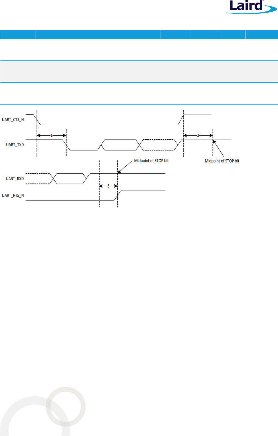
Table 10 and Figure 2 shows UART timing of specifications.
BT860
Datasheet
Embedded Wireless Solutions Support Center:
http://ews-support.lairdtech.com
www.lairdtech.com/bluetooth
11
© Copyright 2017 Laird. All Rights Reserved
Americas: +1-800-492-2320
Europe: +44-1628-858-940
Hong Kong: +852 2923 0610
Table 10: UART timing specifications
Reference
Characteristics Min. Typ. Max. Unit
1 Delay time
UART_CTS_N low to UART TXD valid - - 1.50 Bit
periods
2 Setup time
UART_CTS_N high before midpoint of stop bit - - 0.67 Bit
periods
3 Delay time
Midpoint of stop bit to UART_CTS_N high - - 1.33 Bit
periods
Figure 2: UART timing
8.3. PCM Interface
The BT860 supports two independent PCM interfaces that share the pins with I2S interfaces. The PCM interface
on the BT860 can connect to linear PCM Codec devices in master or slave mode. In master mode, the BT860
generates the PCM_CLK and PCM_SYNC signals, and in slave mode, these signals are provided by another
master on the PCM interface and are inputs to the BT860.
The configuration of the PCM interface may be adjusted by the host using vendor-specific HCI commands.
8.3.1. Slot Mapping
The BT860 supports up to three simultaneous full-duplex SCO or eSCO channels through the PCM interface.
These three channels are time-multiplexed onto the single PCM interface by using a time-slotting scheme where
the 8 kHz or 16 kHz audio sample interval is divided into as many as 16 slots. The number of slots is dependent
on the selected interface rate of 128 kHz, 512 kHz, or 1024 kHz. The corresponding number of slots for these
interface rate is 1, 2, 4, 8 and 16, respectively. Transmit and receive PCM data from an SCO channel is always
mapped to the same slot. The PCM data output driver tristates its output on unused slots to allow other devices
to share the same PCM interface signals. The data output driver tristates its output after the falling edge of the
PCM clock during the last bit of the slot.
BT860
Datasheet
Embedded Wireless Solutions Support Center:
http://ews-support.lairdtech.com
www.lairdtech.com/bluetooth
12
© Copyright 2017 Laird. All Rights Reserved
Americas: +1-800-492-2320
Europe: +44-1628-858-940
Hong Kong: +852 2923 0610
8.3.2. Frame Synchronization
The BT860 supports both short- and long-frame synchronization in both master and slave modes. In short-frame
synchronization mode, the frame synchronization signal uses an active-high pulse at the audio frame rate that is
a single-bit period in width and is synchronized to the rising edge of the bit clock. The PCM slave looks for a high
on the falling edge of the bit clock and expects the first bit of the first slot to start at the next rising edge of the
clock.
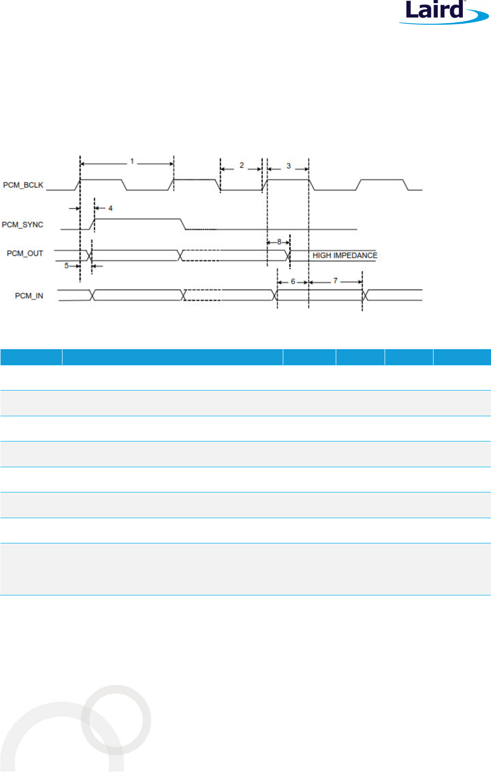
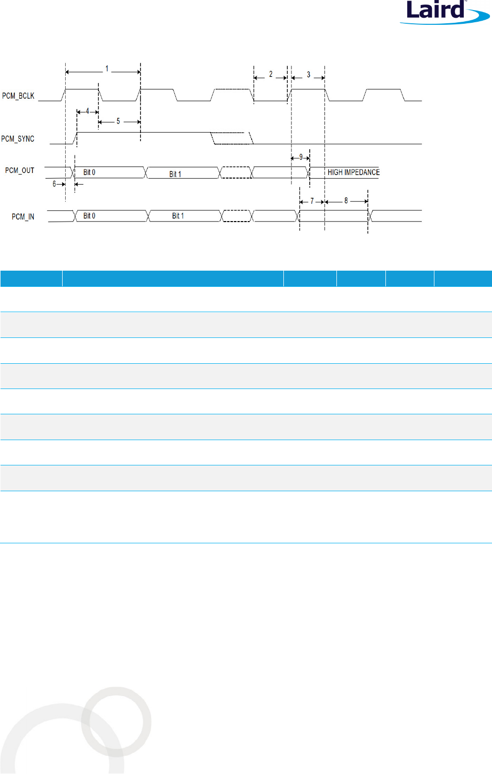
Figure 3 and Table 11 shows PCM Timing Diagram and Specifications for the master mode of short-frame.
Figure 3: PCM timing diagram (Short-Frame Sync, Master Mode)
Table 11: PCM Interface timing specifications (Short-Frame Sync, Master Mode)
Reference
Characteristics Min. Typ. Max. Unit
1 PCM bit clock frequency - - 12 MHz
2 PCM bit clock LOW 41 - - ns
3 PCM bit clock HIGH 41 - - ns
4 PCM_SYNC setup 0 - 25 ns
5 PCM_OUT delay 0 - 25 ns
6 PCM_IN setup 8 - - ns
7 PCM_IN hold 8 - - ns
8
Delay from rising edge of PCM_BCLK during last
bit period to PCM_OUT becoming high
impedance
0 - 25 ns
BT860
Datasheet
Embedded Wireless Solutions Support Center:
http://ews-support.lairdtech.com
www.lairdtech.com/bluetooth
13
© Copyright 2017 Laird. All Rights Reserved
Americas: +1-800-492-2320
Europe: +44-1628-858-940
Hong Kong: +852 2923 0610
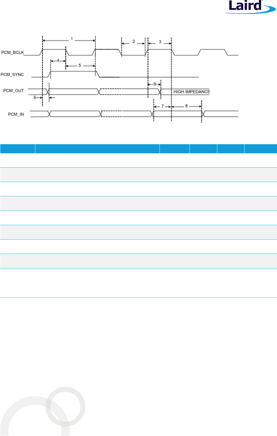
Figure 4 and Table 12 shows PCM Timing Diagram and Specifications for the slave mode of short-frame.
Figure 4: PCM timing diagram (Short-Frame Sync, Slave Mode)
Table 12: PCM Interface timing specifications (Short-Frame Sync, Slave Mode)
Reference
Characteristics Min. Typ. Max. Unit
1 PCM bit clock frequency - - 12 MHz
2 PCM bit clock LOW 41 - - ns
3 PCM bit clock HIGH 41 - - ns
4 PCM_SYNC setup 8 - - ns
5 PCM_SYNC_hold 8 - - ns
6 PCM_OUT delay 0 - 25 ns
7 PCM_IN setup 8 - - ns
8 PCM_IN hold 8 - - ns
9
Delay from rising edge of PCM_BCLK during last
bit period to PCM_OUT becoming high
impedance
0 - 25 ns
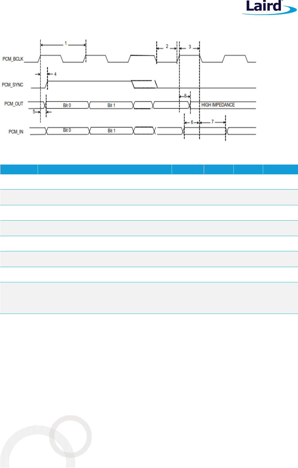
In long-frame synchronization mode, the frame synchronization signal is again an active-high pulse at the audio
frame rate; however, the duration is three bit periods and the pulse starts coincident with the first bit of the first
slot.
BT860
Datasheet
Embedded Wireless Solutions Support Center:
http://ews-support.lairdtech.com
www.lairdtech.com/bluetooth
14
© Copyright 2017 Laird. All Rights Reserved
Americas: +1-800-492-2320
Europe: +44-1628-858-940
Hong Kong: +852 2923 0610
Figure 5 through Table 13 shows PCM Timing Diagram and Specifications for the master mode of long-frame.
Figure 5: PCM timing diagram (Long-Frame Sync, Master Mode)
Table 13: PCM Interface timing specifications (Long-Frame Sync, Master Mode)
Reference
Characteristics Min. Typ. Max. Unit
1 PCM bit clock frequency - - 12 MHz
2 PCM bit clock LOW 41 - - ns
3 PCM bit clock HIGH 41 - - ns
4 PCM_SYNC delay 0 - 25 ns
5 PCM_OUT delay 0 - 25 ns
6 PCM_IN setup 8 - - ns
7 PCM_IN hold 8 - - ns
8
Delay from rising edge of PCM_BCLK during last
bit period to PCM_OUT becoming high
impedance
0 - 25 ns
BT860
Datasheet
Embedded Wireless Solutions Support Center:
http://ews-support.lairdtech.com
www.lairdtech.com/bluetooth
15
© Copyright 2017 Laird. All Rights Reserved
Americas: +1-800-492-2320
Europe: +44-1628-858-940
Hong Kong: +852 2923 0610
Figure 6 and Table 14 shows PCM Timing Diagram and Specifications for the slave mode of long-frame
Figure 6: PCM timing diagram (Long-Frame Sync, Slave Mode)
Table 14: PCM Interface timing specifications (Long-Frame Sync, Slave Mode)
Reference
Characteristics Min. Typ. Max. Unit
1 PCM bit clock frequency - - 12 MHz
2 PCM bit clock LOW 41 - - ns
3 PCM bit clock HIGH 41 - - ns
4 PCM_SYNC setup 8 - - ns
5 PCM_SYNC_hold 8 - - ns
6 PCM_OUT delay 0 - 25 ns
7 PCM_IN setup 8 - - ns
8 PCM_IN hold 8 - - ns
9
Delay from rising edge of PCM_BCLK during last
bit period to PCM_OUT becoming high
impedance
0 - 25 ns
8.3.3.
Data Formatting
The BT860 may be configured to generate and accept several different data formats. For conventional
narrowband speech mode, the BT860 uses 13 of the 16 bits in each PCM frame. The location and order of these
13 bits can be configured to support various data formats on the PCM interface. The remaining three bits are
ignored on the input and may be filled with 0s, 1s, a sign bit, or a programmed value on the output. The default
format is 13-bit 2’s complement data, left justified, and clocked MSB first.
BT860
Datasheet
Embedded Wireless Solutions Support Center:
http://ews-support.lairdtech.com
www.lairdtech.com/bluetooth
16
© Copyright 2017 Laird. All Rights Reserved
Americas: +1-800-492-2320
Europe: +44-1628-858-940
Hong Kong: +852 2923 0610
8.3.4. Wideband Speech Support
When the host encodes Wideband Speech (WBS) packets in transparent mode, the encoded packets are
transferred over the PCM bus for an eSCO voice connection. In this mode, the PCM bus is typically configured in
master mode for a 4 kHz sync rate with 16-bit samples, resulting in a 64 Kbps bit rate. The BT860 also supports
slave transparent mode using a proprietary rate-matching scheme. In SBC-code mode, linear 16-bit data at 16
kHz (256Kbps rate) is transferred over the PCM bus.
8.3.5.
Multiplexed Bluetooth Over PCM
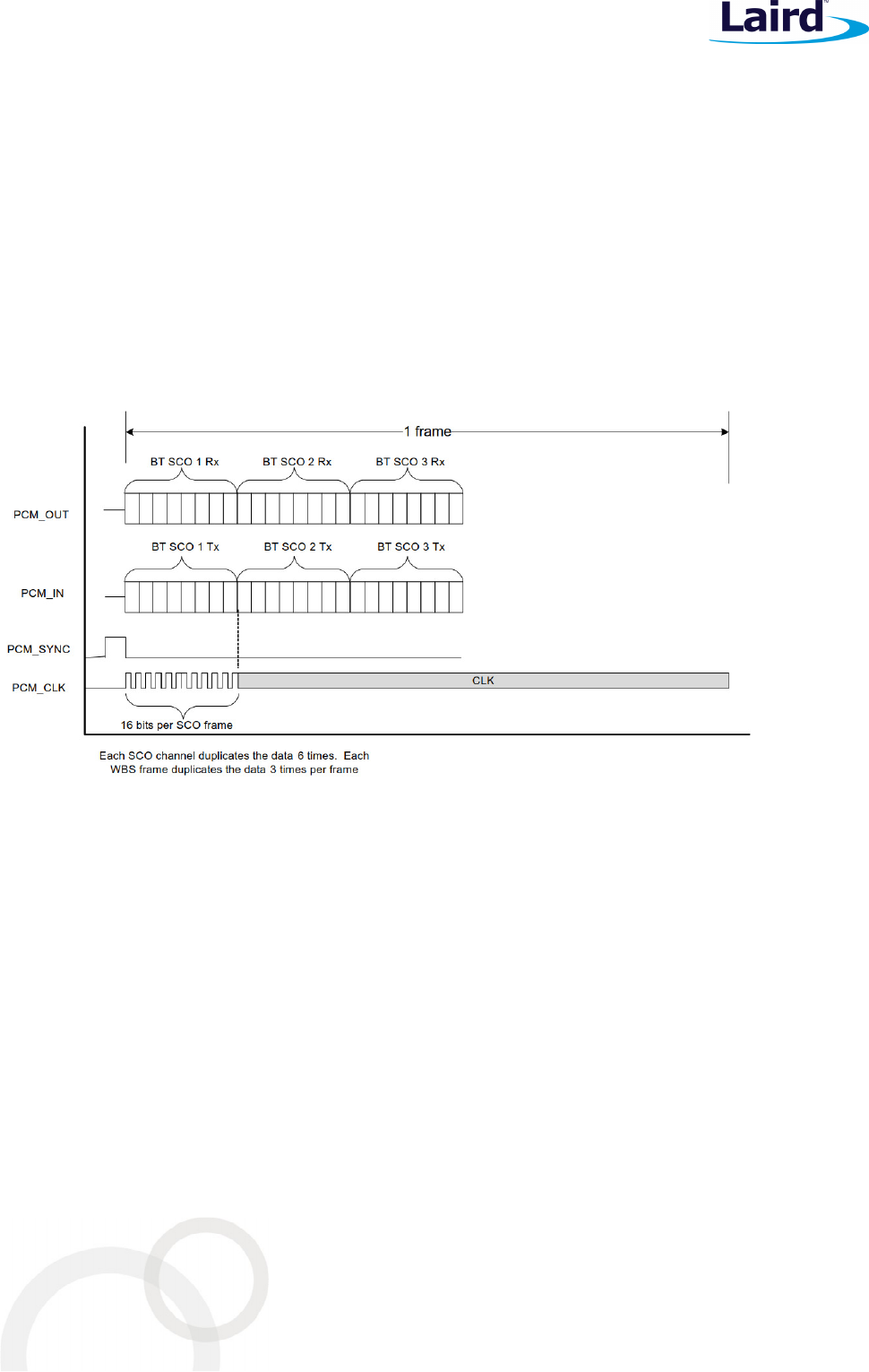
Bluetooth supports multiple audio streams within the Bluetooth channel and both 16 kHz and 8 kHz streams can
be multiplexed. This mode of operation is only supported when the Bluetooth host is the master. Figure7 shows
the operation of the multiplexed transport with three simultaneous SCO connections. To accommodate
additional SCO channels, the transport clock speed is increased. To change between modes of operation, the
transport must be halted and restarted in the new configuration.
Figure 7: Functional Multiples Data diagram
8.3.6. Burst PCM Mode
In this mode of operation, the PCM bus runs at a significantly higher rate of operation to allow the host to duty
cycle its operation and save current. In this mode of operation, the PCM bus can operate at a rate of up to 24
MHz. This mode of operation is initiated with an HCI command from the host.
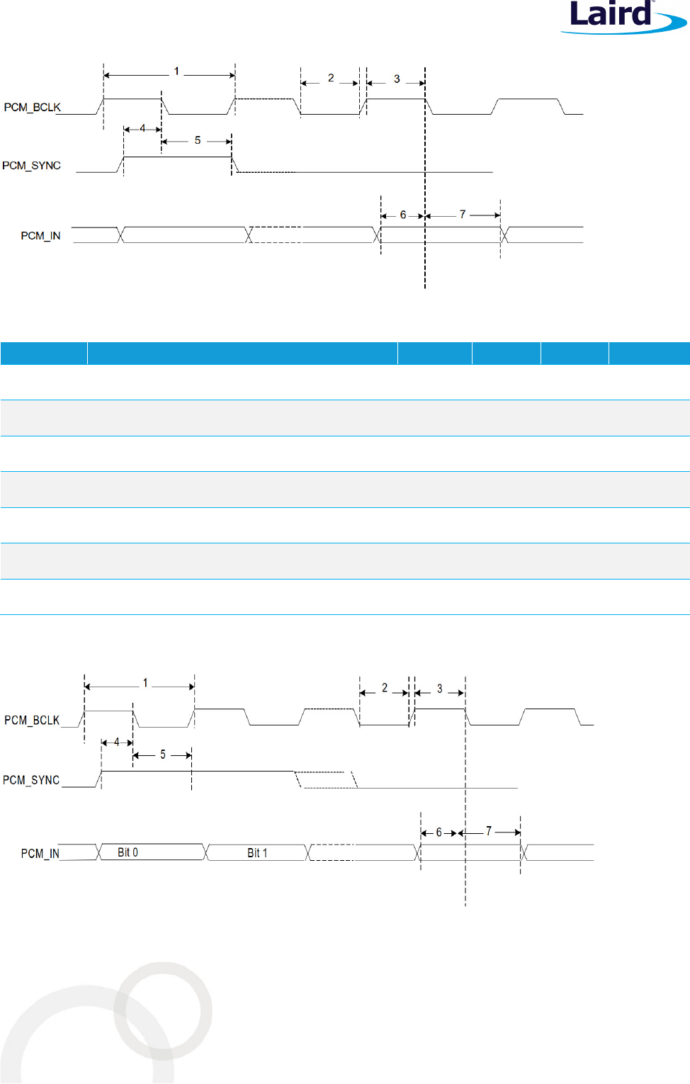
Figure 8 and Table 15 shows PCM Burst mode timing diagram and specifications for the receive-only mode of
short-frame sync.
BT860
Datasheet
Embedded Wireless Solutions Support Center:
http://ews-support.lairdtech.com
www.lairdtech.com/bluetooth
17
© Copyright 2017 Laird. All Rights Reserved
Americas: +1-800-492-2320
Europe: +44-1628-858-940
Hong Kong: +852 2923 0610
Figure 8: PCM Burst Mode timing (Receive Only, Short Frame Sync)
Table 15: PCM Burst Mode Specifications (Receive Only, Short-Frame Sync)
Reference
Characteristics Min. Typ. Max. Unit
1 PCM bit clock frequency - - 24 MHz
2 PCM bit clock LOW 20.8 - - ns
3 PCM bit clock HIGH 20.8 - - ns
4 PCM_SYNC setup 8 - - ns
5 PCM_SYNC_hold 8 - - ns
6 PCM_IN setup 8 - - ns
7 PCM_IN hold 8 - - ns
Figure 9 and Table 16 shows PCM Burst mode timing diagram and specifications for the receive-only mode of
long-frame sync.
Figure 9: PCM Burst Mode Timing (Receive Only, Long Frame Sync)

BT860
Datasheet
Embedded Wireless Solutions Support Center:
http://ews-support.lairdtech.com
www.lairdtech.com/bluetooth
18
© Copyright 2017 Laird. All Rights Reserved
Americas: +1-800-492-2320
Europe: +44-1628-858-940
Hong Kong: +852 2923 0610
Table 16: PCM Burst Mode Specifications (Receive Only, Long-Frame Sync)
Reference
Characteristics Min. Typ. Max. Unit
1 PCM bit clock frequency - - 24 MHz
2 PCM bit clock LOW 20.8 - - ns
3 PCM bit clock HIGH 20.8 - - ns
4 PCM_SYNC setup 8 - - ns
5 PCM_SYNC_hold 8 - - ns
6 PCM_IN setup 8 - - ns
7 PCM_IN hold 8 - - ns
8.4. I
2
S Interface
The BT860 supports two independent I
2
S digital audio ports. The I
2
S interface supports both master and slave
modes. The I
2
S signals are:
I
2
S clock: I
2
S SCK
I
2
S Word Select: I
2
S WS
I
2
S Data Out: I
2
S SDO
I
2
S Data In: I
2
S SDI
I
2
S SCK and I
2
S WS become outputs in master mode and inputs in slave mode, while I
2
S SDO always stays as an
output. The channel word length is 16 bits and the data is justified so that the MSB of the left-channel data is
aligned with the MSB of the I
2
S bus, per the I
2
S specification. The MSB of each data word is transmitted one bit
clock cycle after the I
2
S WS transition, synchronous with the falling edge of bit clock. Left-channel data is
transmitted when I
2
S WS is low, and right-channel data is transmitted when I
2
S WS is high. Data bits sent by the
BT860 are synchronized with the falling edge of I2S_SCK and should be sampled by the receiver on the rising
edge of I2S_SSCK.
The clock rate in master mode is either of the following:
48 kHz x 32 bits per frame = 1.536 MHz
48 kHz x 50 bits per frame = 2.400 MHz
The master clock is generated from the input reference clock using a N/M clock divider.
In the slave mode, any clock rate is supported to a maximum of 3.072 MHz.
BT860
Datasheet
Embedded Wireless Solutions Support Center:
http://ews-support.lairdtech.com
www.lairdtech.com/bluetooth
19
© Copyright 2017 Laird. All Rights Reserved
Americas: +1-800-492-2320
Europe: +44-1628-858-940
Hong Kong: +852 2923 0610
8.4.1. I
2
S Timing
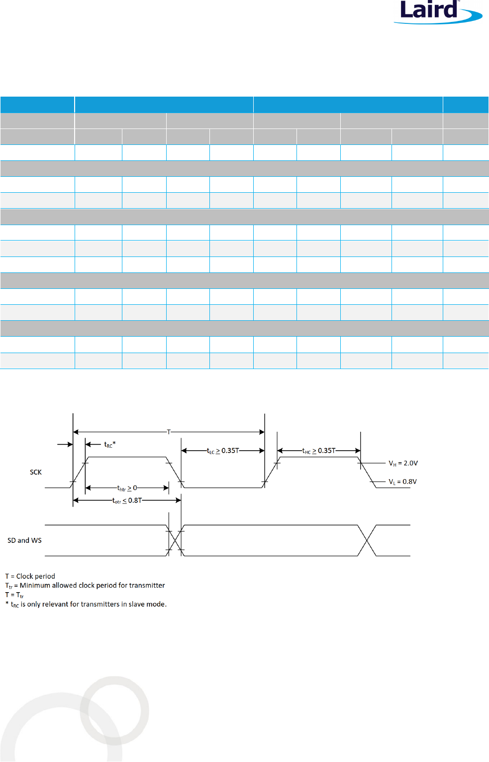
Timing values specified in Table 17 are relative to high and low threshold levels.
Table 17: Timing for I2S Transmitters and Receivers
Transmitter Receiver Notes
Lower Limit Upper Limit Lower Limit Upper Limit
Min Max Min Max Min Max Min Max
Clock Period T
T
tr
- - - T
r
- - -
Master Mode: Clock generated by transmitter or receiver
HIGH t
HC
0.35T
tr
- - - 0.35T
tr
- - -
LOW t
LC
0.35T
tr
- - - 0.35T
tr
- - -
Master Mode: Clock generated by transmitter or receiver
HIGH t
HC
- 0.35T
tr
- - - 0.35T
tr
- -
LOW t
LC
- 0.35T
tr
- - - 0.35T
tr
- -
Rise time t
RC
- - 0.15T
tr
- - - - -
Transmitter
Delay t
dtr
- - - 0.8T - - - -
Hold time t
htr
0 - - - - - - -
Receiver
Setup time t
sr
- - - - - 0.2T
r
- -
Hold time t
hr
- - - - - 0 - -
The time periods specified in Figure 10 and Figure 11 are defined by the transmitter speed. The receiver
specifications must match transmitter performance.
Figure 10: I
2
S Transmitter timing
BT860
Datasheet
Embedded Wireless Solutions Support Center:
http://ews-support.lairdtech.com
www.lairdtech.com/bluetooth
20
© Copyright 2017 Laird. All Rights Reserved
Americas: +1-800-492-2320
Europe: +44-1628-858-940
Hong Kong: +852 2923 0610
Figure 11: I
2
S Receiver Timing
8.5. BSC (Cypress Serial Control) Master Interface
BT860 includes a Cypress Serial Control (BSC) master interface. The BSC interface supports low-speed and fast
mode devices and is compatible with I
2
C slave devices. Multiple I
2
C master devices and flexible wait state
insertion by the master interface or slave devices are not supported. The BT860 provides 400 kHz, full speed
clock support.
The BSC interface is programmed by the CPU to generate the following BSC transfer types on the bus:
Read-only
Write-only
Combined read/write
Combined write-read
NVRAM may contain configuration information about the customer application, including the following:
Fractional-N information
BD_ADDR
UART baud rate
USB enumeration information
SDP service record
File system information used for code, code patches, or data
Figure 12 and Table 18 define the timing requirements for the BSC interface.
Figure 12: BSC Interface Timing Diagram
BT860
Datasheet
Embedded Wireless Solutions Support Center:
http://ews-support.lairdtech.com
www.lairdtech.com/bluetooth
21
© Copyright 2017 Laird. All Rights Reserved
Americas: +1-800-492-2320
Europe: +44-1628-858-940
Hong Kong: +852 2923 0610
Table 18: BSC Interface Timing Specifications
Reference Characteristics Min. Max. Unit
1 Clock frequency -
100
400
800
1000
kHz
2 START condition setup time 650 - ns
3 START condition hold time 280 - ns
4 Clock low time 650 - ns
5 Clock high time 280 - ns
6 Data input hold time 0 - ns
7 Data input setup time 100 - ns
8 STOP condition setup time 280 - ns
9 Output valid from clock - 400 ns
10 Bus free time 650 - ns
9 A
NTENNA
P
ERFORMANCE
Table 19, Figure 13, and Figure 14 show the antenna gain and performance.
Table 19: Antenna gain
Unit in dBi @ 2440MHz XY-Plane XZ-Plane YZ-Plane Efficiency
AT3216-B2R7HAA Peak Avg. Peak Avg. Peak Avg.
1.7 -2.9 2.3 -2.3 0.2 -5.4 55%
Figure 13: Antenna Return Loss
BT860
Datasheet
Embedded Wireless Solutions Support Center:
http://ews-support.lairdtech.com
www.lairdtech.com/bluetooth
22
© Copyright 2017 Laird. All Rights Reserved
Americas: +1-800-492-2320
Europe: +44-1628-858-940
Hong Kong: +852 2923 0610
Figure 14: Antenna pattern
BT860
Datasheet
Embedded Wireless Solutions Support Center:
http://ews-support.lairdtech.com
www.lairdtech.com/bluetooth
23
© Copyright 2017 Laird. All Rights Reserved
Americas: +1-800-492-2320
Europe: +44-1628-858-940
Hong Kong: +852 2923 0610
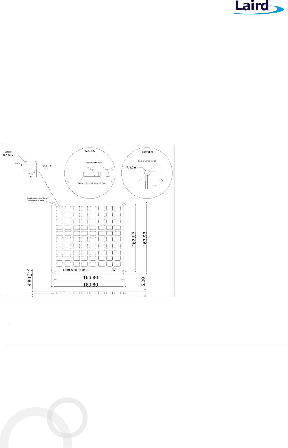
10 M
ECHANICAL
D
IMENSIONS AND
L
AND
P
ATTERN
10.1. BT860 Mechanical Drawing
Note: Dimensions are in millimetres.
Tolerances: .xx ±0.03 mm
.x ±1.3 mm
Dimensions from corner of BT860
Pin1
BT860
Datasheet
Embedded Wireless Solutions Support Center:
http://ews-support.lairdtech.com
www.lairdtech.com/bluetooth
24
© Copyright 2017 Laird. All Rights Reserved
Americas: +1-800-492-2320
Europe: +44-1628-858-940
Hong Kong: +852 2923 0610
11 I
MPLEMENTATION
N
OTE
11.1. PCB Layout on Host PCB
Checklist (for PCB):
M
UST
locate the BT860 module close to the edge of PCB.
Use solid GND plane on inner layer (for best EMC and RF performance).
Place GND vias close to module GND pads as possible
Route traces to avoid noise being picked up on VCC supply.
Antenna Keep-out area:
– Ensure there is no copper in the antenna keep-out area on any layers of the host PCB.
– Keep all mounting hardware and metal clear of the area to allow proper antenna radiation.
– For best antenna performance, place the BT860 module on the edge of the host PCB, preferably in the
corner with the antenna facing the corner.
– A different host PCB thickness dielectric will have small effect on antenna.
Figure 15: Recommend Antenna keep-out area (in Blue) used on the BT860
11.1.1. Antenna Keep-out and Proximity to Metal or Plastic
Checklist (for metal /plastic enclosure):
Minimum safe distance for metals without seriously compromising the antenna (tuning) is 40 mm
top/bottom and 30 mm left or right.
Metal close to the BT860 chip monopole antenna (bottom, top, left, right, any direction) will have
degradation on the antenna performance. The amount of degradation is entirely system dependent which
means some testing by customers is required (in their host application).
Any metal closer than 20 mm starts to significantly degrade performance (S11, gain, radiation efficiency).
It is best that the customer tests the range with mock-up (or actual prototype) of the product to assess
effects of enclosure height (and material whether metal or plastic).
BT860
Datasheet
Embedded Wireless Solutions Support Center:
http://ews-support.lairdtech.com
www.lairdtech.com/bluetooth
25
© Copyright 2017 Laird. All Rights Reserved
Americas: +1-800-492-2320
Europe: +44-1628-858-940
Hong Kong: +852 2923 0610
12 A
PPLICATION
N
OTE FOR
S
URFACE
M
OUNT
M
ODULES
12.1. Introduction
Laird surface mount modules are designed to conform to all major manufacturing guidelines. This application
note is intended to provide additional guidance beyond the information that is presented in the user manual.
This application note is considered a living document and is updated as new information is presented.
The modules are designed to meet the needs of a number of commercial and industrial applications. They are
easy to manufacture and they conform to current automated manufacturing processes.
12.2. Shipping
12.2.1. Tray Package
Modules are shipped in ESD (Electrostatic Discharge) safe trays that can be loaded into most manufacturers pick
and place machines. Layouts of the trays are provided in Figure 16.
Figure 16: Shipping tray layout
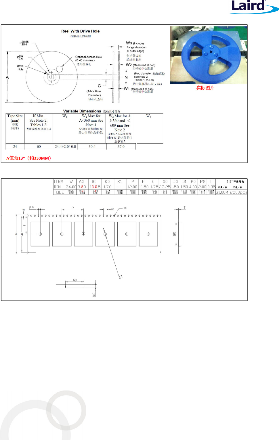
12.2.2. Tape and Reel Package Information
Note: Ordering information for Tape and Reel packaging is an addition of T/R to the end of the full
module part number. For example, BT860 becomes BT860-Sx-xx-T/R.
BT860
Datasheet
Embedded Wireless Solutions Support Center:
http://ews-support.lairdtech.com
www.lairdtech.com/bluetooth
26
© Copyright 2017 Laird. All Rights Reserved
Americas: +1-800-492-2320
Europe: +44-1628-858-940
Hong Kong: +852 2923 0610
Figure 17: Reel specifications
Figure 18: Tape specifications
There are 2500 BT860 modules taped in a reel (and packaged in a pizza box) and five boxes per carton (12,500
modules per carton). Reel, boxes, and carton are labeled with the appropriate labels. See Figure 19.
BT860
Datasheet
Embedded Wireless Solutions Support Center:
http://ews-support.lairdtech.com
www.lairdtech.com/bluetooth
27
© Copyright 2017 Laird. All Rights Reserved
Americas: +1-800-492-2320
Europe: +44-1628-858-940
Hong Kong: +852 2923 0610
12.2.3. Packaging Process
Figure 19: BT860 packaging process
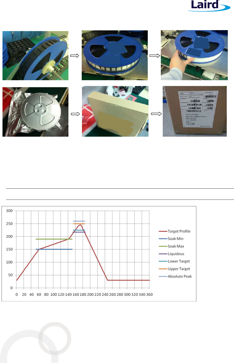
12.3. Reflow Parameters
Laird surface mount modules are designed to be easily manufactured, including reflow soldering to a PCB.
Ultimately it is the responsibility of the customer to choose the appropriate solder paste and to ensure oven
temperatures during reflow meet the requirements of the solder paste. Laird’s surface mount modules conform
to J-STD-020D1 standards for reflow temperatures.
Important: During reflow, modules should not be above 260° and not for more than 30 seconds.
Figure 20: Recommended reflow temperature

BT860
Datasheet
Embedded Wireless Solutions Support Center:
http://ews-support.lairdtech.com
www.lairdtech.com/bluetooth
28
© Copyright 2017 Laird. All Rights Reserved
Americas: +1-800-492-2320
Europe: +44-1628-858-940
Hong Kong: +852 2923 0610
Temperatures should not exceed the minimums or maximums presented in Table 20.
Table 20: Recommended maximum and minimum temperatures
Specification
Value
Unit
Temperature Inc./Dec. Rate (max)
1~3 °C / Sec
Temperature Decrease rate (goal)
2-4 °C / Sec
Soak Temp Increase rate (goal)
.5 - 1 °C / Sec
Flux Soak Period (Min)
70 Sec
Flux Soak Period (Max)
120 Sec
Flux Soak Temp (Min)
150 °C
Flux Soak Temp (max)
190 °C
Time Above Liquidous (max)
70 Sec
Time Above Liquidous (min)
50 Sec
Time In Target Reflow Range (goal)
30 Sec
Time At Absolute Peak (max)
5 Sec
Liquidous Temperature (SAC305)
218 °C
Lower Target Reflow Temperature
240 °C
Upper Target Reflow Temperature
250 °C
Absolute Peak Temperature
260 °C
13 J
APAN
(MIC)
R
EGULATORY
The BT800 is approved for use in the Japanese market. The part numbers listed below hold WW type
certification. Refer to ARIB-STD-T66 for further guidance on OEM’s responsibilities.
Model Product Name Description Certificate Number
BT860-SA
BT860-ST
BT v4.2 Dual Mode UART HCI
Module
Mounted with chipset antenna 201-170971
13.1. Antenna Information
The BT800 was tested with antennas listed below. The OEM can choose a different manufacturers antenna but
must make sure it is of same type and that the gain is lesser than or equal to the antenna that is approved for
use.
Item
Part Number Mfg. Type Gain (dBi)
1 AT3216-B2R7HAA
ACX Ceramic 0.5
2 001-0030 mFlexPIFA LAIRD PIFA 2
3 001-0014 FlexPIFA LAIRD PIFA 2
4 0600-00040 LAIRD Dipole 2
5 NanoBlue MAF94045 LAIRD PCB Dipole 2

BT860
Datasheet
Embedded Wireless Solutions Support Center:
http://ews-support.lairdtech.com
www.lairdtech.com/bluetooth
29
© Copyright 2017 Laird. All Rights Reserved
Americas: +1-800-492-2320
Europe: +44-1628-858-940
Hong Kong: +852 2923 0610
14 FCC
R
EGULATORY
Model US/FCC CANADA/IC
BT860-SA SQGBT850
BT860-ST SQGBT850
DVK-BT860-SA
DVK-BT860-ST
The BT85x family has been designed to operate with the antenna listed below having a maximum gain of 0.5 dBi.
The required antenna impedance is 50 ohms.
Item Part Number Mfg. Type Gain (dBi)
1 AT3216-B2R7HAA
ACX Ceramic 0.5
2 001-0030 mFlexPIFA LAIRD PIFA 2
3 001-0014 FlexPIFA LAIRD PIFA 2
4 0600-00040 LAIRD Dipole 2
5 NanoBlue MAF94045 LAIRD PCB Dipole 2
14.1. Documentation Requirements
To ensure regulatory compliance, when integrating the BT860 into a host device, it is necessary to meet the
documentation requirements set forth by the applicable regulatory agencies. The following sections (FCC,
Industry Canada, and European Union) outline the information that may be included in the user’s guide and
external labels for the host devices into which the BT860 is integrated.
IMPORTANT:
If the conditions above cannot be met (for example certain device configurations or co
-
lo
cation with
another transmitter), then the FCC authorization is no longer considered valid and the FCC ID cannot
be used on the final product. In these circumstances, the OEM integrator will be responsible for re-
evaluating the end product (including the transmitter) and obtaining a separate FCC authorization.
When using Laird’s FCC grant for the BT860, the integrator must include specific information in the
user’s guide for the device into which the BT860 is integrated. The integrator must not provide
information to the end user regarding how to install or remove this RF module in the user’s manual of
the device into which the BT860 is integrated. The following FCC statements must be added in their
entirety and without modification into a prominent place in the user’s guide for the device into which
the BT860 is integrated:
IMPORTANT NOTE: To comply with FCC requirements, the BT860 must not be co-located or
operating in conjunction with any other antenna or transmitter.
This device is intended only for OEM integrators under the following conditions:
The transmitter module may not be co-located with any other transmitter or antenna,
If the condition above is met, further transmitter test will not be required. However, the OEM
integrator is still responsible for testing their end-product for any additional compliance requirements
required with this module installed

BT860
Datasheet
Embedded Wireless Solutions Support Center:
http://ews-support.lairdtech.com
www.lairdtech.com/bluetooth
30
© Copyright 2017 Laird. All Rights Reserved
Americas: +1-800-492-2320
Europe: +44-1628-858-940
Hong Kong: +852 2923 0610
Important Note:
If these conditions cannot be met (for example, certain laptop configurations or co-location with
another transmitter), then the FCC authorization is no longer considered valid and the FCC ID
cannot be used on the final product. In these circumstances, the OEM integrator will be
responsible for re-evaluating the end product (including the transmitter) and obtaining a separate
FCC authorization.
End Product Labeling
The final end product must be labeled in a visible area with the following: Contains FCC ID: SQGBT850.
Manual Information to the End User
The OEM integrator must be aware to not provide information to the end user regarding how to install
or remove this RF module in the user’s manual of the end product which integrates this module.
The end user manual shall include all required regulatory information/warning as show in this manual.
Federal Communication Commission Interference Statement
This equipment has been tested and found to comply with the limits for a Class B digital device,
pursuant to Part 15 of the FCC Rules. These limits are designed to provide reasonable protection
against harmful interference in a residential installation. This equipment generates, uses, and can
radiate radio frequency energy and, if not installed and used in accordance with the instructions, may
cause harmful interference to radio communications. However, there is no guarantee that interference
will not occur in a particular installation. If this equipment does cause harmful interference to radio or
television reception, which can be determined by turning the equipment off and on, the user is
encouraged to try to correct the interference by one of the following measures:
Reorient or relocate the receiving antenna.
Increase the separation between the equipment and receiver.
Connect the equipment into an outlet on a circuit different from that to which the receiver is
connected.
Consult the dealer or an experienced radio/TV technician for help.
FCC Caution: Any changes or modifications not expressly approved by the party responsible for
compliance could void the user's authority to operate this equipment.
This device complies with Part 15 of the FCC Rules. Operation is subject to the following two
conditions: (1) This device may not cause harmful interference, and (2) this device must accept any
interference received, including interference that may cause undesired operation.
IMPORTANT NOTE: FCC Radiation Exposure Statement:
This equipment complies with the US portable RF exposure limit set forth for an uncontrolled
environment and are safe for intended operation as described in this manual. The further RF exposure
reduction can be achieved if the product can be kept as far as possible from the user body or set the
device to lower output power if such function is available.
This transmitter must not be co-located or operating in conjunction with any other antenna or
transmitter.

BT860
Datasheet
Embedded Wireless Solutions Support Center:
http://ews-support.lairdtech.com
www.lairdtech.com/bluetooth
31
© Copyright 2017 Laird. All Rights Reserved
Americas: +1-800-492-2320
Europe: +44-1628-858-940
Hong Kong: +852 2923 0610
15 I
NDUSTRY
C
ANADA
R
EGULATORY
This device complies with Industry Canada’s license-exempt RSSs. Operation is subject to the following two
conditions:
1. This device may not cause interference; and
2. This device must accept any interference, including interference that may cause undesired operation of
the device.
Le présent appareil est conforme aux CNR d’Industrie Canada applicables aux appareils radio exempts de licence.
L’exploitation est autorisée aux deux conditions suivantes:
1. l’appareil ne doit pas produire de brouillage;
2. l’appareil doit accepter tout brouillage radioélectrique subi, même si le brouillage est susceptible d’en
compromettre le fonctionnement.
Radiation Exposure Statement:
The product complies with the Canada portable RF exposure limit set forth for an uncontrolled environment and
are safe for intended operation as described in this manual. The further RF exposure reduction can be achieved
if the product can be kept as far as possible from the user body or set the device to lower output power if such
function is available.
Déclaration d'exposition aux radiations:
Le produit est conforme aux limites d'exposition pour les appareils portables RF pour les Etats-Unis et le Canada
établies pour un environnement non contrôlé. Le produit est sûr pour un fonctionnement tel que décrit dans ce
manuel. La réduction aux expositions RF peut être augmentée si l'appareil peut être conservé aussi loin que
possible du corps de l'utilisateur ou que le dispositif est réglé sur la puissance de sortie la plus faible si une telle
fonction est disponible.
This device is intended only for OEM integrators under the following conditions:
The transmitter module may not be co-located with any other transmitter or antenna.
If the condition above is met, further transmitter test will not be required. However, the OEM integrator is still
responsible for testing their end-product for any additional compliance requirements required with this module
installed.
Cet appareil est conçu uniquement pour les intégrateurs OEM dans les conditions suivantes:
Le module émetteur peut ne pas être coïmplanté avec un autre émetteur ou antenne.
Tant que les 1 condition ci-dessus sont remplies, des essais supplémentaires sur l'émetteur ne seront pas
nécessaires. Toutefois, l'intégrateur OEM est toujours responsable des essais sur son produit final pour toutes
exigences de conformité supplémentaires requis pour ce module installé.
I
MPORTANT
N
OTE
:
If these conditions cannot be met (for example, certain laptop configurations or co-location with another
transmitter), then the Canada authorization is no longer considered valid and the IC ID cannot be used on the
final product. In these circumstances, the OEM integrator will be responsible for re-evaluating the end product
(including the transmitter) and obtaining a separate Canada authorization.

BT860
Datasheet
Embedded Wireless Solutions Support Center:
http://ews-support.lairdtech.com
www.lairdtech.com/bluetooth
32
© Copyright 2017 Laird. All Rights Reserved
Americas: +1-800-492-2320
Europe: +44-1628-858-940
Hong Kong: +852 2923 0610
NOTE IMPORTANTE:
Dans le cas où ces conditions ne peuvent être satisfaites (par exemple pour certaines configurations
d'ordinateur portable ou de certaines co-localisation avec un autre émetteur), l'autorisation du Canada n'est
plus considéré comme valide et l'ID IC ne peut pas être utilisé sur le produit final. Dans ces circonstances,
l'intégrateur OEM sera chargé de réévaluer le produit final (y compris l'émetteur) et l'obtention d'une
autorisation distincte au Canada.
End Product Labeling
The final end product must be labeled in a visible area with the following: “Contains IC: 3147A-BT850”.
Plaque signalétique du produit final
Le produit final doit être étiqueté dans un endroit visible avec l'inscription suivante: "Contient des IC: 3147A-
BT850".
Manual Information to the End User
The OEM integrator must be aware not to provide information to the end user regarding how to install or
remove this RF module in the user’s manual of the end product which integrates this module.
The end user manual shall include all required regulatory information/warning as show in this manual.
Manuel d'information à l'utilisateur final
L'intégrateur OEM doit être conscient de ne pas fournir des informations à l'utilisateur final quant à la façon
d'installer ou de supprimer ce module RF dans le manuel de l'utilisateur du produit final qui intègre ce module.
Le manuel de l'utilisateur final doit inclure toutes les informations réglementaires requises et avertissements
comme indiqué dans ce manuel.
This radio transmitter (IC: 3147A-BT850) has been approved by Industry Canada to operate with the antenna
types listed below with the maximum permissible gain indicated. Antenna types not included in this list, having a
gain greater than the maximum gain indicated for that type, are strictly prohibited for use with this device.
Le présent émetteur radio (IC: 3147A-BT850) a été approuvé par Industrie Canada pour fonctionner avec les
types d'antenne énumérés cidessous et ayant un gain admissible maximal. Les types d'antenne non inclus dans
cette liste, et dont le gain est supérieur au gain maximal indiqué, sont strictement interdits pour l'exploitation de
l'émetteur.
16 E
UROPEAN
U
NION
R
EGULATORY
The BT800 has been tested for compliance with relevant standards for the EU market. BT800 module was tested
with a 0.5 dBi chip antenna.
The OEM should consult with a qualified test house before entering their device into an EU member country to
make sure all regulatory requirements have been met for their complete device.
Reference the Declaration of Conformities listed below for a full list of the standards that the modules were
tested to. Test reports are available upon request.
BT860
Datasheet
Embedded Wireless Solutions Support Center:
http://ews-support.lairdtech.com
www.lairdtech.com/bluetooth
33
© Copyright 2017 Laird. All Rights Reserved
Americas: +1-800-492-2320
Europe: +44-1628-858-940
Hong Kong: +852 2923 0610
16.1. EU Declarations of Conformity
Manufacturer Laird
Products BT860-SA and BT860-ST
Product
Description Bluetooth v4.2 Class 1 UART HCI
EU Directives 2014/53/EU – Radio Equipment Directive (RED)
Reference standards used for presumption of conformity:
Article Number
Requirement Reference standard(s)
3.1a
Low voltage equipment safety
EN 60950-1:2006 +A11:2009 +A1:2010 +A12:2011
+A2:2013
RF Exposure EN 62311:2008
EN 62479:2010
3.1b
Protection requirements with
respect to electromagnetic
compatibility
EN 301 489-1 v2.2.0 (2017-03)
EN 301 489-17 v3.2.0 (2017-03)
3.2 Means of the efficient use of
the radio frequency spectrum
EN 300 328 v2.1.1 (2016-11)
Declaration:
We, Laird, declare under our sole responsibility that the essential radio test suites have been carried out and
that the above product to which this declaration relates is in conformity with all the applicable essential
requirements of Article 3 of the EU Directive 1999/5/EC, when used for its intended purpose.
Place of Issue:
Laird
W66N220 Commerce Court, Cedarburg, WI 53012 USA
tel: +1-262-375-4400 fax: +1-262-364-2649
Date of Issue: May 2017
Name of Authorized Person: Thomas T Smith, Director of EMC Compliance
Signature of Authorized Person:
17 O
RDERING
I
NFORMATION
Part Number Description
BT860-SA BTv4.2 Dual Mode UART HCI Module with integrated Antenna
BT860-ST BTv4.2 Dual Mode UART HCI Module – Trace Pin
DVK-BT860 Development Kit for BT860 Module
17.1. General Comments
This is a preliminary datasheet. Please check with Laird for the latest information before commencing a design. If
in doubt, ask.
BT860
Datasheet
Embedded Wireless Solutions Support Center:
http://ews-support.lairdtech.com
www.lairdtech.com/bluetooth
34
© Copyright 2017 Laird. All Rights Reserved
Americas: +1-800-492-2320
Europe: +44-1628-858-940
Hong Kong: +852 2923 0610
18 B
LUETOOTH
SIG
A
PPROVALS
18.1. Application Note: Subsystem Combinations
This application note covers the procedure for generating a new Declaration ID for a Subsystem combination on
the Bluetooth SIG website. In the instance of subsystems, a member can combine two or more subsystems to
create a complete Bluetooth End Product solution.
Subsystem listings referenced as an example:
Design Name
Owner
Declaration ID
Link to listing on the SIG website
BT860-SA Laird B021369 https://www.bluetooth.org/tpg/QLI_viewQDL.cfm?qid=21369
Windows 8
(Host Subsystem)
Microsoft
Corporation
B012854 https://www.bluetooth.org/tpg/QLI_viewQDL.cfm?qid=12854
Laird Customer Declaration ID Procedure
This procedure assumes that the member is simply combining two subsystems to create a new design, without
any modification to the existing, qualified subsystems. This is achieved by using the Listing interface on the
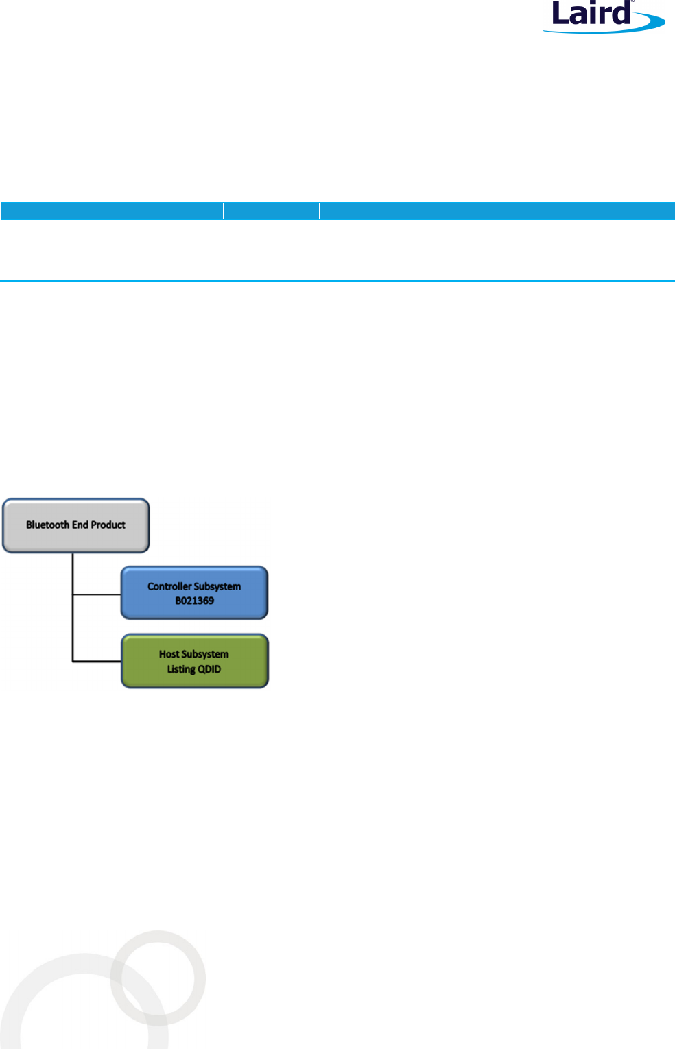
Bluetooth SIG website. Error! Reference source not found. shows the basic subsystem combination of a
controller and host subsystem. The Controller provides the RF/BB/LM and HCI layers, with the Host providing
L2CAP, SDP, GAP, RFCOMM/SPP and any other specific protocols and profiles existing in the Host subsystem
listing. The design may also include a Profile Subsystem.
The controller provides the RF/BB/LM and HCI layers, with the Host providing L2CAP, SDP, GAP, RFCOMM/SPP
and any other specific protocols and profiles existing in the Host subsystem listing. The design may also include a
Profile Subsystem.
Figure 21: Basic subsystem combination of a controller and host subsystem
The Qualification Process requires each company to registered as a member of the Bluetooth SIG –
http://www.bluetooth.org
The following link provides a link to the Bluetooth Registration page: https://www.bluetooth.org/login/register/
For each Bluetooth Design it is necessary to purchase a Declaration ID. This can be done before starting the new
qualification, either through invoicing or credit card payment. The fees for the Declaration ID will depend on
your membership status, please refer to the following webpage:
https://www.bluetooth.org/en-us/test-qualification/qualification-overview/fees

BT860
Datasheet
Embedded Wireless Solutions Support Center:
http://ews-support.lairdtech.com
www.lairdtech.com/bluetooth
35
© Copyright 2017 Laird. All Rights Reserved
Americas: +1-800-492-2320
Europe: +44-1628-858-940
Hong Kong: +852 2923 0610
For a detailed procedure of how to obtain a new Declaration ID for your design, please refer to the following SIG
document:
https://www.bluetooth.org/DocMan/handlers/DownloadDoc.ashx?doc_id=283698&vId=317486
To start the listing, go to: https://www.bluetooth.org/tpg/QLI_SDoc.cfm.
In step 1, select the option, Reference a Qualified Design and enter the Declaration IDs of each subsystem used
in the End Product design. You can then select your pre-paid Declaration ID from the drop down menu or go to
the Purchase Declaration ID page, (please note that unless the Declaration ID is pre-paid or purchased with a
credit card, it will not be possible to proceed until the SIG invoice is paid.
Once all the relevant sections of step 1 are finished, complete steps 2, 3, and 4 as described in the help
document. Your new Design will be listed on the SIG website and you can print your Certificate and DoC.
For further information please refer to the following training material:
https://www.bluetooth.org/en-us/test-qualification/qualification-overview/listing-process-updates
19 A
DDITIONAL
A
SSISTANCE
Please contact your local sales representative or our support team for further assistance:
Laird Technologies Connectivity Products Business Unit
Support Centre:
http://ews-support.lairdtech.com
Email:
wireless.support@lairdtech.com
Phone: Americas: +1-800-492-2320
Europe: +44-1628-858-940
Hong Kong: +852 2923 0610
Web:
http://www.lairdtech.com/bluetooth
© Copyright 2017 Laird. All Rights Reserved. Patent pending. Any information furnished by Laird and its agents is believed to be accurate and
reliable. All specifications are subject to change without notice. Responsibility for the use and application of Laird materials or products rests
with the end user since Laird and its agents cannot be aware of all potential uses. Laird makes no warranties as to non-infringement nor as to
the fitness, merchantability, or sustainability of any Laird materials or products for any specific or general uses. Laird, Laird Technologies, Inc., or
any of its affiliates or agents shall not be liable for incidental or consequential damages of any kind. All Laird products are sold pursuant to the
Laird Terms and Conditions of Sale in effect from time to time, a copy of which will be furnished upon request. When used as a tradename
herein,
Laird
means Laird PLC or one or more subsidiaries of Laird PLC. Laird™, Laird Technologies™, corresponding logos, and other marks are
trademarks or registered trademarks of Laird. Other marks may be the property of third parties. Nothing herein provides a license under any
Laird or any third party intellectual property right.