Laird Connectivity RM191 RM191-SM User Manual Revised v0 4

Laird Technologies RM191-SM Users Manual Revised v0 4

Users Manual Revised v0_4
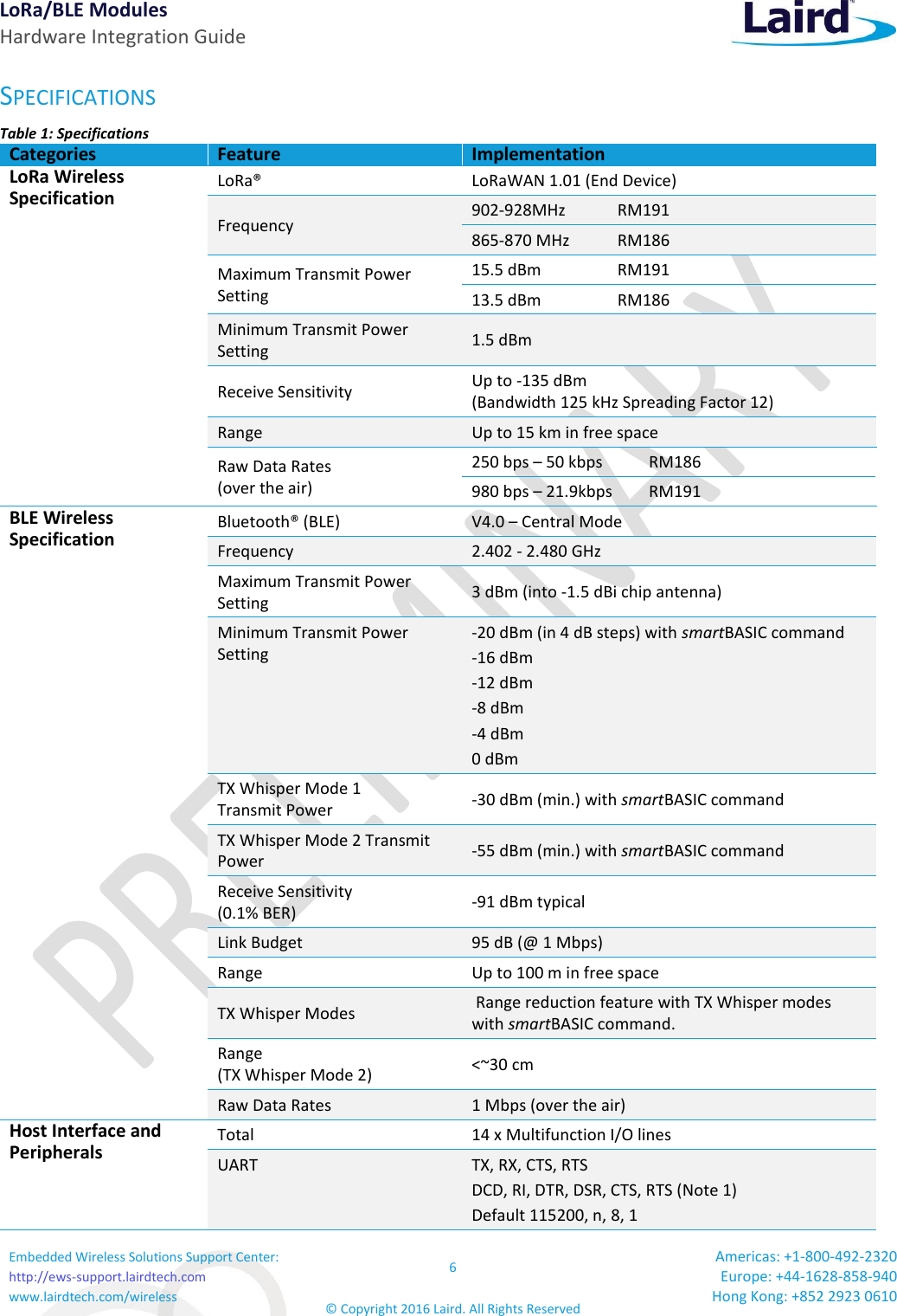
A     Hardware Integration Guide LoRa/Bluetooth Low Energy (BLE) Module Part Numbers: RM186 and RM191 Preliminary Version 0.04
LoRa/BLE Modules Hardware Integration Guide Embedded Wireless Solutions Support Center: http://ews-support.lairdtech.com www.lairdtech.com/wireless 2 © Copyright 2016 Laird. All Rights Reserved Americas: +1-800-492-2320 Europe: +44-1628-858-940 Hong Kong: +852 2923 0610  REVISION HISTORY Version Date Notes Approver 0.01 28 Mar 2016 Preliminary Release Jonathan Kaye 0.02 31 Mar 2016 Deleted Note 3 for power supply rise time in section ”Recommended Operating Parameters” Modified section “FCC and IC Regulatory Statements“ John Talley 0.03 28 April 2016 Updated Max Transmit power, temperatures, and DVK descriptions. Jonathan Kaye 0.04 29 April 2016 Update to IC Radiation Exposure Statement, Operating temperatures. John Talley
LoRa/BLE Modules Hardware Integration Guide Embedded Wireless Solutions Support Center: http://ews-support.lairdtech.com www.lairdtech.com/wireless 3 © Copyright 2016 Laird. All Rights Reserved Americas: +1-800-492-2320 Europe: +44-1628-858-940 Hong Kong: +852 2923 0610  CONTENTS Overview and Key Features ........................................................................................................................................5 Features and Benefits .............................................................................................................................................5 Application Areas ....................................................................................................................................................5 Specifications ..............................................................................................................................................................6 Hardware Specifications .............................................................................................................................................9 Block Diagram and Pin-out .....................................................................................................................................9 Pin Definitions ..................................................................................................................................................... 10 Electrical Specifications ....................................................................................................................................... 12 Absolute Maximum Ratings............................................................................................................................. 12 Recommended Operating Parameters ............................................................................................................ 12 nAutoRUN Pin and Operating Modes .............................................................................................................. 14 LoRa Power Consumption ....................................................................................................................................... 15 BLE Power Consumption ......................................................................................................................................... 15 BLE Measured Peak Current Waveforms during Connection ............................................................................. 17 Peripheral Block Current Consumption ............................................................................................................... 17 Functional Description ............................................................................................................................................. 18 Power Management (includes brown-out and power on reset) ........................................................................ 18 Clocks and Timers ................................................................................................................................................ 19 Clocks ............................................................................................................................................................... 19 Timers .............................................................................................................................................................. 19 Memory for smartBASIC Application Code ......................................................................................................... 19 RF ......................................................................................................................................................................... 19 UART Interface .................................................................................................................................................... 19 SPI Bus ................................................................................................................................................................. 20 I2C Interface ........................................................................................................................................................ 21 General Purpose I/O, ADC and PWM/FREQ ........................................................................................................ 21 GPIO ................................................................................................................................................................. 21 ADC .................................................................................................................................................................. 21 PWM and FREQ Signal Output on up to Two SIO Pins .................................................................................... 22 nRESET Pin ........................................................................................................................................................... 22 nAutoRUN Pin ...................................................................................................................................................... 22 Two-Wire SWD Programming/Debug Interface .................................................................................................. 22 RM1xx on-board chip antenna characteristics .................................................................................................... 23 Hardware Integration Suggestions .......................................................................................................................... 23 Circuit .................................................................................................................................................................. 23 PCB Layout on Host PCB - General ...................................................................................................................... 25 Antenna Keep-out on Host PCB ....................................................................................................................... 25 Antenna Keep-out and Proximity to Metal or Plastic ...................................................................................... 26 LoRa External Antenna Integration with RM1xx ................................................................................................. 27 Mechanical Details .................................................................................................................................................. 27 RM1xx Mechanical Details .................................................................................................................................. 27 Host PCB Land Pattern and Antenna Keep-out for RM1xx.................................................................................. 28 Application Note for Surface Mount Modules ........................................................................................................ 28 Introduction ......................................................................................................................................................... 28 Shipping ............................................................................................................................................................... 29
LoRa/BLE Modules Hardware Integration Guide Embedded Wireless Solutions Support Center: http://ews-support.lairdtech.com www.lairdtech.com/wireless 4 © Copyright 2016 Laird. All Rights Reserved Americas: +1-800-492-2320 Europe: +44-1628-858-940 Hong Kong: +852 2923 0610  Reflow Parameters .............................................................................................................................................. 29 FCC and IC Regulatory Statements .......................................................................................................................... 31 Power Exposure Information............................................................................................................................... 32 OEM Responsibilities ........................................................................................................................................... 32 CE Regulatory .......................................................................................................................................................... 34 Antenna Information ........................................................................................................................................... 35 EU Declarations of Conformity ................................................................................................................................ 36 RM186-SM ........................................................................................................................................................... 36 Ordering Information .............................................................................................................................................. 37 General Comments .............................................................................................................................................. 37 Bluetooth SIG Qualification ..................................................................................................................................... 37 Overview .............................................................................................................................................................. 37 Qualification Steps When Deviating From a Laird End Product Design .............................................................. 38 Additional Assistance .......................................................................................................................................... 39
LoRa/BLE Modules Hardware Integration Guide Embedded Wireless Solutions Support Center: http://ews-support.lairdtech.com www.lairdtech.com/wireless 5 © Copyright 2016 Laird. All Rights Reserved Americas: +1-800-492-2320 Europe: +44-1628-858-940 Hong Kong: +852 2923 0610  OVERVIEW AND KEY FEATURES This Hardware Integration Guide describes both the RM186 (868MHz band for EU) and RM191 (915MHz band for US). The differences will be outlined in the Radio Specifications. Every RM1xx Series module is designed to enable OEMs to add a long range LoRa radio link as well as central role Bluetooth Low Energy (BLE) to small, portable, power-conscious devices. The RM1xx modules are enabled with Laird’s smart BASIC, an event-driven programming language that enables OEMs to make their product development quicker and simpler, significantly reducing time to market. smartBASIC enables customers to develop a complete embedded application inside the compact RM1xx hardware, connecting to a wide array of external sensors via its I2C, SPI, UART, ADC or GPIO interfaces. Based on the world-leading Nordic Semiconductor nRF51822 (BLE) and Semtech Sx1272 (LoRa) chipsets, the RM1xx modules provide ultra-low power consumption with outstanding wireless range using the LoRa radio link and local BLE connections via 3 dBm of transmit power. This document should be read in conjunction with the smart BASIC user manual. Note:   This is a PRELIMINARY version of the RM1xx Hardware Integration Guide. Information in this document is subject to change. Please contact Laird to obtain the most recent version of this document – http://ews-support.lairdtech.com. Features and Benefits  Application Areas  Bluetooth v4.0 – Central Mode  On Board BLE Chip Antenna  u.FL for external LoRa antenna  smartBASIC programming language   Bluetooth SIG Listed   Compact Footprint  Long Range LoRa range up to 15km  BLE Programmable TX power +3 dBm to -20 dBm  BLE TX whisper mode (-30 dBm, -55 dBm)  BLE RX sensitivity: -91 dBm  Ultra-low power consumption  BLE TX: 11.6 mA peak (at +3 dBm) (See Note 4 in the Power Consumption section)  BLE RX: 8.8 mA peak (See Note 4 in the Power Consumption section)  Standby Doze: TBD  Deep Sleep: TBD (See Note 4 in the Power Consumption section)  UART, GPIO, ADC, PWM FREQ output, TIMERS, I2C, and SPI interfaces  Fast Time to Market  FCC/IC (RM191-SM), CE (RM186-SM)  No external components required  Public or Private Networks   Irrigation / Agriculture  Parking  Lighting  Asset Tracking  Tank Monitoring  Smart Home – smoke alarms, heating,   Access Control – security  Industrial Automation – Factory   Any long range, battery powered sensor application!
LoRa/BLE Modules Hardware Integration Guide Embedded Wireless Solutions Support Center: http://ews-support.lairdtech.com www.lairdtech.com/wireless 6 © Copyright 2016 Laird. All Rights Reserved Americas: +1-800-492-2320 Europe: +44-1628-858-940 Hong Kong: +852 2923 0610  SPECIFICATIONS Table 1: Specifications Categories Feature Implementation LoRa Wireless  Specification LoRa®  LoRaWAN 1.01 (End Device) Frequency 902-928MHz  RM191 865-870 MHz   RM186 Maximum Transmit Power Setting 15.5 dBm RM191 13.5 dBm RM186 Minimum Transmit Power Setting 1.5 dBm Receive Sensitivity  Up to -135 dBm  (Bandwidth 125 kHz Spreading Factor 12)  Range Up to 15 km in free space Raw Data Rates  (over the air) 250 bps – 50 kbps RM186 980 bps – 21.9kbps RM191 BLE Wireless  Specification Bluetooth® (BLE) V4.0 – Central Mode Frequency 2.402 - 2.480 GHz Maximum Transmit Power Setting 3 dBm (into -1.5 dBi chip antenna) Minimum Transmit Power Setting -20 dBm (in 4 dB steps) with smartBASIC command -16 dBm -12 dBm -8 dBm -4 dBm 0 dBm TX Whisper Mode 1  Transmit Power -30 dBm (min.) with smartBASIC command TX Whisper Mode 2 Transmit Power -55 dBm (min.) with smartBASIC command Receive Sensitivity  (0.1% BER) -91 dBm typical  Link Budget  95 dB (@ 1 Mbps) Range Up to 100 m in free space TX Whisper Modes     Range reduction feature with TX Whisper modes with smartBASIC command.  Range  (TX Whisper Mode 2)     <~30 cm Raw Data Rates 1 Mbps (over the air) Host Interface and Peripherals Total 14 x Multifunction I/O lines UART TX, RX, CTS, RTS DCD, RI, DTR, DSR, CTS, RTS (Note 1) Default 115200, n, 8, 1
LoRa/BLE Modules Hardware Integration Guide Embedded Wireless Solutions Support Center: http://ews-support.lairdtech.com www.lairdtech.com/wireless 7 © Copyright 2016 Laird. All Rights Reserved Americas: +1-800-492-2320 Europe: +44-1628-858-940 Hong Kong: +852 2923 0610  Categories Feature Implementation From 1,200 to 460800 bps GPIO Up to 14  With configurable I/O direction, O/P drive strength (standard 0.5 mA or high 5 mA), pull-up/pull-down ADC Four 10-bit channels (including ADC reference) 10 bit resolution 1.2 V internal reference  1/1, 2/3, 1/3 pre-scaling PWM or FREQ output PWM or FREQ output on up to two GPIO output pins: PWM output duty cycle 0%-100% PWM output frequency Up to 500 kHz (Note 7) FREQ output frequency 0 MHz-4 MHz  (50% duty cycle) I2C One I2C interface (up to 400 kbps) (Note 2) SPI One SPI Master interface (up to 4 Mbps) (Note 3) Services Services supported  GATT client and capabilities                         FW Upgrade smartBASIC runtime engine FW upgrade (1) Via UART (2) Via 2-Wire SWD Programming/Debug Interface Programmability smartBASIC On-board programming language similar to BASIC.   smartBASIC application  download (1) Via UART. (2) Via 2-Wire SWD Programming/Debug Interface       Control Protocols Any   User defined via smartBASIC Operating Modes Self-contained Run mode Selected by nAutoRun pin status:  nAutoRun = LOW (0V): Then runs $autorun$ (smartBASIC application script) if it exists. Interactive / development mode nAutoRun = HIGH (VCC): Then runs via at+run (and “file name” of smartBASIC application script). Supply Voltage Supply (VCC) 2.1V – 3.5V Internal DCDC converter (Note 5) 1.8V – 2.1V Internal LDO DCDC switched on if VCC >2.1V at power-up Power Consumption Active modes peak current  (for Max TX PWR 3 dBm)  Connected mode   11.6 mA peak TX  8.9 mA peak RX                 Active modes peak current  (for TX Whisper mode2 PWR -55 dBm)   Connected mode      5 mA peak TX 8.5 mA peak RX                 Active modes average current Depends on many factors. See Power Consumption.  Ultra-low power modes Standby Doze     Deep Sleep                   2.6 uA typical (Note 6) 600 nA (Note 6) Antenna Options BLE (Internal) chip antenna  On-board ceramic chip monopole antenna  -1.5 dBi LoRa (External)  Dipole antenna with U.FL (IPEX) connector up to 2 dBi
LoRa/BLE Modules Hardware Integration Guide Embedded Wireless Solutions Support Center: http://ews-support.lairdtech.com www.lairdtech.com/wireless 8 © Copyright 2016 Laird. All Rights Reserved Americas: +1-800-492-2320 Europe: +44-1628-858-940 Hong Kong: +852 2923 0610  Categories Feature Implementation Physical Dimensions 25.4 mm x 25.4 mm x 3.1 mm  Weight 3 grams Environmental Operating -40 ˚C to +85 ˚C   (VCC 1.8V – 3.5 V) Storage -40 ˚C to +85 ˚C Miscellaneous Lead Free Lead-free and RoHS compliant Warranty 5-Year Limited Lifetime Development Tools Development Kit Development Kit DVK-RM1xx and  Free Software Tools Approvals Bluetooth® SIG Listed – Declaration ID FCC / IC / CE  RM191-SM: FCC/IC,  RM186-SM: CE Note 1:  DSR, DTR, RI, and DCD can be implemented in the smart BASIC application.                           Note 2:   With I2C interface selected, pull-up resistors on I2C SDA and I2C SCL MUST be connected    externally as per I2C standard.   Note 3:   SPI interface (master) consists of SPI MOSI, SPI MISO and SPI CLK. SPI CS is created by      customer using any spare SIO pin within their smartBASIC application script allowing multi-   dropping.                                          Note 4:   RM1xx module comes loaded with smart BASIC runtime engine FW, but does not come      loaded with any smart BASIC application script (as that is dependent on customer end      application or use). Laird provides many sample smart BASIC application scripts covering the    services listed. Additional applications being added every quarter.   Note 5:   Laird suggests using Vcc of 3.3V +/-5% (3.13V-3.46V) for maximum LoRa output power.    WARNING:  above 3.5V, the LoRa transmitter will be disabled to maintain regulatory compliance Note 6:   Deep Sleep current <1000nA (typical).                           Standby Doze current TBD (typical).   Note 7:   PWM output signal has a frequency and duty cycle property.  PWM output is generated     using 32-bit hardware timers. The timers are clocked by a 1MHz (1uS period) clock source.     Trade-off PWM output frequency with resolution. For example:                                                                                       PWM output frequency of 500kHz (2uS) results in resolution of 1:2                                           PWM output frequency of 100kHz (10uS) results in resolution of 1:10                                         PWM output frequency of 10kHz (100uS) results in resolution of 1:100                                    PWM output frequency of 1kHz(1000uS) results in resolution of 1:1000                                   Refer to the smartBASIC user guide for details.
LoRa/BLE Modules Hardware Integration Guide Embedded Wireless Solutions Support Center: http://ews-support.lairdtech.com www.lairdtech.com/wireless 9 © Copyright 2016 Laird. All Rights Reserved Americas: +1-800-492-2320 Europe: +44-1628-858-940 Hong Kong: +852 2923 0610  HARDWARE SPECIFICATIONS Block Diagram and Pin-out  Figure 1: Functional HW and SW block diagram for RM1xx series smartBASIC modules  Figure 2: RM186/RM191 module pin-out (top view)
LoRa/BLE Modules Hardware Integration Guide Embedded Wireless Solutions Support Center: http://ews-support.lairdtech.com www.lairdtech.com/wireless 10 © Copyright 2016 Laird. All Rights Reserved Americas: +1-800-492-2320 Europe: +44-1628-858-940 Hong Kong: +852 2923 0610  Pin Definitions Table 2: Pin definitions Pin # Pin  Name Default Function Alt. Funct. Default Direction Note14 Pull-up/ Pull-down Note14 Notes Comment 1 GND - - - - - - 2 SIO_21 DIO UART TX OUT Set high in FW 1,2,4,6,7 UARTCLOSE() selects DIO functionality and UARTOPEN() selects UART comms behaviour 3 SIO_22 DIO UART RX IN PULL-UP 1,2,4,6,7 4 SIO_23 DIO UART RTS OUT Set low in FW 1,2,4,6,7 5 SIO_24 DIO UART CTS IN PULL-DOWN 1,2,4,6,7 6 SIO_25 nAutoRUN/DIO DIO IN NONE IN ONLY Laird Devkit, UART_DSR via J10, J12 7 SIO_28 DIO - IN PULL-UP 13,1,2,6 Laird DevKit: J6 8 GND - - - - -  9 SIO_29 DIO I2C SCL IN PULL-UP 1,2,6,11 I2COPEN() in smartBASIC selects I2C function 10 SIO_30 DIO I2C SDA IN PULL-UP 1,2,6,11 11 GND        12 VCC_BLE - - - - - Vcc for BLE Radio 13 VCC_LORA - - - - - Vcc for Lora Radio 14 GND - - - - -  15 SIO_00 DIO SPI CLK IN PULL-UP 1,2,6,11 SPIOPEN() in smartBASIC selects SPI function, MOSI and CLK will be outputs when in SPI master mode. See note 11 16 SIO_17 DIO SPI MISO IN PULL-UP 1,2,6,11 17 SIO_03/AIN DIO/AIN SPI MOSI IN PULL-UP 1,2,3,4,5,6,11 18 SIO_04/AIN DIO AIN IN PULL-UP 1,2,3,4,5,6,11 Laird Devkit: SPI Slave Select 19 SIO_05/AIN DIO AIN IN PULL-UP 1,2,3,4,5,6,11 Laird Devkit: Button2 or Ana Temp Sensor via J7 20 SIO_06/AIN DIO AIN IN PULL-UP 1,2,3,4,5,6,11 Laird Devkit: LED5 or Arduino A0 Via J8 21 GND       22 nRESET   IN  9,10 System Reset (Active low) 23 NC     9 DO NOT CONNECT 24 GND
LoRa/BLE Modules Hardware Integration Guide Embedded Wireless Solutions Support Center: http://ews-support.lairdtech.com www.lairdtech.com/wireless 11 © Copyright 2016 Laird. All Rights Reserved Americas: +1-800-492-2320 Europe: +44-1628-858-940 Hong Kong: +852 2923 0610  Note 1:  Secondary function is selectable in smartBASIC application. Note 2:   DIO = Digital Input or Output. I/O voltage level tracks VCC. Note 3:   AIN = Analog Input  Note 4:   DIO or AIN functionality is selected using the GpioSetFunc() function in smartBASIC. Note 5:   AIN configuration selected using GpioSetFunc() function. Note 6:  I2C, UART, SPI controlled by xxxOPEN() functions in smart BASIC. Note 7:  SIO_21 to SIO_24 are DIO by default when $autorun$ app runs on power up. Note 8:  N/A    Note 9:  Hidden 2-Wire SWD Programming/Debug Interface, pin22 (SWDIO) and pin23 (SWDCLK). Used for upgrading smartBASIC runtime engine FW with J-link programmer. Using this hidden 2-Wire SWD Programming/Debug Interface on customers host PCB requires header connector Samtec FTSH-105-01-L-DV, refer to section 2-Wire SWD Programming/Debug Interface for details.  Note 10: Pull the nRESET pin (pin 22) low for minimum 100 mS to reset the module. Note11:  SPI CS is created by customer using any spare SIO pin within their smartBASIC application script allowing multi-dropping.    Note12:  N/A    Note13:  N/A   Note14:  smart BASIC runtime engine has DIO (Default Function) INPUT pins, have by default PULL-UP enabled.  This was done to avoid floating inputs (which can also cause current consumption in low power modes (e.g. StandbyDoze) to drift with time.  In any case customer can disable the PUL-UP through their smart BASIC application.          All the SIO pins (with a default function of DIO are inputs – apart from SIO_21 and SIO_23, which are outputs):   - SIO_21 (alternative function UART_TX) is an output, set high (in FW). - SIO_23 (alternative function UART_RTS) is an output, set low (in FW). - SIO_22 (alternative function UART_RX) is an input, set with internal pull-up (in FW). - SIO_24 (alternative function UART_CTS) is an input, set with internal pull-down (in FW).  The RM1xx module is delivered with the integrated smartBASIC runtime engine FW loaded (but no onboard smartBASIC application script). Because of this, it starts up in AT command mode by default.  At reset, all SIO lines are configured as the defaults shown above.   SIO lines can be configured through the smart BASIC application script to be either inputs or outputs with pull-ups or pull-downs. When an alternative SIO function is selected (such as I2C or SPI), the firmware does not allow
LoRa/BLE Modules Hardware Integration Guide Embedded Wireless Solutions Support Center: http://ews-support.lairdtech.com www.lairdtech.com/wireless 12 © Copyright 2016 Laird. All Rights Reserved Americas: +1-800-492-2320 Europe: +44-1628-858-940 Hong Kong: +852 2923 0610  the setup of internal pull-up/pull-down. Therefore, when I2C interface is selected, pull-up resistors on I2C SDA and I2C SCL MUST be connected externally as per I2C standard. UART_RX, UART_TX, UART_CTS are Vcc logic levels (if VCC is 3.3 V, i.e. SIO pin I/O levels track VCC). For example, when RX and TX are idle, they sit at 3.3 V (if VCC is 3.3 V). Conversely, handshaking pins CTS and RTS at 0 V are treated as assertions. Pin 6 (nAutoRUN) is an input, with active low logic. In the development kit (DVK-RM1xx-SM) it is connected so that the state is driven by the host’s DTR output line. The nAutoRUN pin must be externally held high or low to select between the following two operating modes:  Self-contained Run mode (nAutoRUN pin held at 0 V).     Interactive / development mode (nAutoRUN pin held at VCC).      smartBASIC runtime engine firmware checks for the status of nAutoRUN during power-up or reset. If it is low and if there is a smartBASIC application script named $autorun$, then the smartBASIC runtime engine FW executes the application script automatically; hence the name Self-contained Run Mode. Electrical Specifications Absolute Maximum Ratings Absolute maximum ratings for supply voltage and voltages on digital and analogue pins of the module are listed below; exceeding these values causes permanent damage (Table 3). Table 3: Maximum Current Ratings Parameter Minimum Maximum Unit Voltage at VCC_BLE & VCC_LORA pin -0.3 +3.6 (Note 1) V Voltage at GND pin   0 V Voltage at SIO pin  -0.3 VCC+0.3 V Storage temperature -40 +85 ºC Note 1:  Absolute Max Rating for VCC pin (max) is 3.6V, however we recommend 3.3V +/-5% as the spec for maximum Vcc. The LoRa transmitter shuts down if the voltage exceeds 3.5V .                           Recommended Operating Parameters Table 4: Power Supply Operating Parameters Parameter Minimum Typical Maximum Unit VCC1  1.8 3 3.5 V VCC Maximum ripple or noise2   10 mV VCC rise time   TBD mS Operating Temperature Range -40 - +85 ºC Note 1:  Internal DCDC is used if VCC >2.1 V on power-up; otherwise internal LDO is used.  If supply voltage is greater than 3.5V, the LoRa transmitter will be disabled. Note 2:   The maximum VCC ripple or noise (at any frequency) that does not disturb the radio.
LoRa/BLE Modules Hardware Integration Guide Embedded Wireless Solutions Support Center: http://ews-support.lairdtech.com www.lairdtech.com/wireless 13 © Copyright 2016 Laird. All Rights Reserved Americas: +1-800-492-2320 Europe: +44-1628-858-940 Hong Kong: +852 2923 0610  Table 5: Signal Levels for Interface, SIO Parameter Minimum Typical Maximum Unit VIH  Input high voltage 0.7VCC  VCC V VIL  Input low voltage VSS  0.3 V VOH Output high voltage        (std. drive, 0.5mA)       (high-drive, 5mA) (Note 1)  VCC-0.3 VCC-0.3   VCC VCC  V V VOL Output low voltage       (std. drive, 0.5mA)       (high-drive, 5mA) (Note 1)  VSS VSS    0.3 0.3  V V Pull up resistance 11 13 16 kΩ Pull down resistance 11 13 16 kΩ Note 1: Maximum number of pins with 5mA high drive is three.  Table 6: SIO pin alternative function AIN (ADC) specification Parameter Minimum Typical Maximum Unit ADC Internal reference voltage  -1.5% 1.2 V +1.5% % ADC pin input  internal selectable scaling   1/1, 1/3, 2/3  Scaling ADC input pin (AIN) voltage maximum without damaging ADC w.r.t VCC  Prescaling   3.3 V  1/1   3.3 V  2/3   3.3 V  1/3   1.8 V  1/1   1.8 V  2/3   1.8 V  1/3           2.4 3.6 3.6 2.1 2.1 2.1    V V V V V V ADC input pin (AIN) voltage maximum without saturating ADC (with 1.2V internal reference)1 1/1 prescaling 2/3 prescaling 1/3 prescaling      1.2 1.8 3.6    V V V Time required to convert single sample in  10bit mode  9bit mode2 8 bit mode2   68 36 20   uS uS uS ADC input impedance (during operation)3
LoRa/BLE Modules Hardware Integration Guide Embedded Wireless Solutions Support Center: http://ews-support.lairdtech.com www.lairdtech.com/wireless 14 © Copyright 2016 Laird. All Rights Reserved Americas: +1-800-492-2320 Europe: +44-1628-858-940 Hong Kong: +852 2923 0610  Note 1:  Stay within internal 1.2 V reference voltage with given prescaling on AIN pin and do not violate ADC maximum input voltage (for damage) for a given VCC, e.g.  If VCC is 1.8 V can only expose AIN pin to 2.1 V (VCC+0.3). Note 2:   Currently, the smartBASIC runtime engine firmware only allows 10-bit mode.  Note 3:   ADC input impedance is estimated mean impedance of the ADC (AIN) pins. The tolerance is +/-20%. The ADC is highly sensitive to the impedance of the source. The ADC (AIN) input impedance is 200k-600k depending on your ADC gain (pre-scaling) setting. Normally, when not sampling, the ADC (AIN) impedance will have very high value and can consider it to be an open circuit. The moment ADC is sampling, ADC(AIN) impedance is 200k-600k. nAutoRUN Pin and Operating Modes Operating modes (refer to the smartBASIC manual for details):  Self-contained mode  Interactive/Development mode Table 7: nAutoRUN pin Signal Name Pin # I/O Comments nAutoRUN (SIO_25) 6 I Input with active low logic. Operating mode selected by nAutoRun pin status: If Low (0V), runs $autorun$ if it exists; If High (VCC), runs via at+run (and “file name” of application). Pin 40 (nAutoRUN) is an input, with active low logic. In the development board (DVK-RM1xx) it is connected so that the state is driven by the host’s DTR output line. nAutoRUN pin needs to be externally held high or low to select between the two RM1xx operating modes:  Self-contained Run mode (nAutoRUN pin held at 0V).      Interactive/Development mode (nAutoRUN pin held at VCC)     smartBASIC runtime engine firmware checks for the status of nAutoRUN during power-up or reset. If it is low and if there is a smartBASIC application named $autorun$ then the smartBASIC runtime engine executes the application automatically; hence the name self-contained run mode.
LoRa/BLE Modules Hardware Integration Guide Embedded Wireless Solutions Support Center: http://ews-support.lairdtech.com www.lairdtech.com/wireless 15 © Copyright 2016 Laird. All Rights Reserved Americas: +1-800-492-2320 Europe: +44-1628-858-940 Hong Kong: +852 2923 0610  LORA POWER CONSUMPTION Data taken at VCC 3.3V with DCDC converter ON (see Note1) at 25ºC. All peripherals turned off except for UART. Table 8: Power consumption Parameter Min Typical Max Unit RM191 TX Currents  TX current @TXpwr= +15 dBm   TX current @TXpwr=  1 dBm  RM186 TX Currents TX current @TXpwr=  13.5dBm TX current @TXpwr=  1 dBm RM1xx Receive Current RX current   50 TBD  38 TBD  13   mA mA  mA mA  mA Note 1:   At VCC = 3.3V, the DCDC converter will be active.                    BLE POWER CONSUMPTION Data taken at VCC 3.3V (see Note1) and 25ºC. Table 9: Power consumption Parameter Min Typical Max Unit Active Mode ‘peak’ current – (Note 1) (Connection)   TX only run peak current @TXpwr= + 3 dBm   TX only run peak current @T pwr=  0 dBm   TX only run peak current @TXpwr= -4 dBm   TX only run peak current @TXpwr= -8 dBm   TX only run peak current @TXpwr= -12 dBm  TX only run peak current @TXpwr= -16 dBm   T X only run peak current @TXpwr= -20 dBm  TX Whisper Mode 1  TX only run peak current @TXpwr= -30 dBm  TX Whisper Mode 2  TX only run peak current @TXpwr= -55 dBm    11.6 8.4 7.1 6.9 6.4 6.1 5.5  5.4  5.0    mA mA mA mA mA mA mA  mA  mA Active Mode        RX only ‘peak’ current   8.7   mA Ultra Low Power Mode1 (Note 2)     Standby Doze      2.6   uA Ultra Low Power Mode2 (Note 3)     Deep Sleep (no RAM retention)     600 (Note 4)   nA
LoRa/BLE Modules Hardware Integration Guide Embedded Wireless Solutions Support Center: http://ews-support.lairdtech.com www.lairdtech.com/wireless 16 © Copyright 2016 Laird. All Rights Reserved Americas: +1-800-492-2320 Europe: +44-1628-858-940 Hong Kong: +852 2923 0610  Parameter Min Typical Max Unit Active Mode Average current (Note 4)      Connection Average Current draw    Max with connection interval (min)   7.5 mS         with connection interval       67.5 mS                Min with connection interval (max) 4000 mS      ~400 ~2.6-4.1      uA uA Note 1:   If VCC reduces to 2.1V (operating range of DCDC), the peak current consumption would increase from 11.6mA to ~15.5mA for TX power setting of +3dBm. Note 2:   RM1xx: Standby Doze current TBD typical.  Standby Doze is entered automatically (when waitevent statement is encountered within a smartBASIC application script). See individual peripherals current consumption in tables in section Peripheral block current consumption 4.3.  Note 3:   In Deep Sleep, everything is disabled and the only wake-up sources are reset and changes on pins on which sense is enabled. A reset is required to exit Deep Sleep. Note 4:   Data taken with TX power 3 dBm and all peripherals off (UART OFF after radio event). Average current consumption depends on a number of factors (including TX power, VCC and accuracy of 16 MHz and 32.768 kHz crystals). With these factors fixed, the largest variable is the connection interval.                                                                 Connection Interval Range: 7.5 ms to 4000 ms in multiples of 1.25 ms.                                                                          For a connection event:                                                                                 - The minimum average current consumption is when the connection interval is large 4000 mS  – The maximum average current consumption is with the shortest connection interval of 7.5 ms; no slave latency.  Other factors that are also related to average current consumption include whether transmitting 6 packets per connection interval & each packet contains 20 bytes (which is the maximum for each packet) and an inaccurate 32 kHz master clock accuracy would increase the average current consumption.
LoRa/BLE Modules Hardware Integration Guide Embedded Wireless Solutions Support Center: http://ews-support.lairdtech.com www.lairdtech.com/wireless 17 © Copyright 2016 Laird. All Rights Reserved Americas: +1-800-492-2320 Europe: +44-1628-858-940 Hong Kong: +852 2923 0610  BLE Measured Peak Current Waveforms during Connection The following figures illustrate BLE current waveforms observed as the RM1xx module performs during connection functionality.    TBD: Update plot  Figure 3: Typical peak current consumption profile with TBD conditions  Note:  In the above picture, UART is ON. X-axis time (1 mS per square), Y-axis current (2 mA per square).  Peripheral Block Current Consumption The values below are calculated for a typical operating voltage of 3 V.  Table 10: UART Power Consumption Parameter Min Typ Max Unit UART Run current @ Max Baud Rate  230  uA UART Run current @ 115200 bps  220  uA UART Run current @ 1200 bps   210  uA UART Baud rate 1200  460800 bps Table 11: SPI Power Consumption Parameter Min Typ Max Unit SPI Master Run current @ 125 kbps  180  uA SPI Master Run current @ 4 Mbps  200  uA SPI bit rate 0.125  4 Mbps Table 12: I2C Power Consumption Parameter Min Typ Max Unit I2C Run current @ 100 kbps  380  uA I2C Run current @ 400 kbps  400  uA I2C Bit rate 100  400 kbps
LoRa/BLE Modules Hardware Integration Guide Embedded Wireless Solutions Support Center: http://ews-support.lairdtech.com www.lairdtech.com/wireless 18 © Copyright 2016 Laird. All Rights Reserved Americas: +1-800-492-2320 Europe: +44-1628-858-940 Hong Kong: +852 2923 0610  Table 13: ADC Power Consumption Parameter Min Typ Max Unit ADC current during conversion   260  uA For asynchronous interface like the UART (asynchronous as the other end can communicate at any time), the UART (on RM1xx) must kept open (by a command in smart BASIC application script) resulting in the base current consumption penalty. For synchronous interface like the I2C or SPI (since RM1xx side is the master), the interface can be closed and opened only (by a command in smart BASIC application script) when needed, resulting in current saving (no base current consumption penalty). Similar argument for ADC (open ADC when needed). FUNCTIONAL DESCRIPTION The RM1xx module is a self-contained LoRa/Bluetooth Low Energy product and requires only power and a user’s smartBASIC application to implement full LoRa and BLE functionality. The LoRa radio in conjunction with its external 2 dBi antenna implements a long range, low data rate connection to a LoRa gateway up to 15 km. The integrated, high performance BLE antenna combined with the RF and base-band circuitry provides the Bluetooth Low Energy wireless link to connect to local BLE sensors. The RM1xx SIO lines provide the OEM’s chosen interface connection to the wired serial/SPI/I2C/analog sensors. The user’s smartBASIC application binds the sensors to the LoRa and BLE wireless functionality. The variety of hardware interfaces and the smartBASIC programming language allow the RM1xx module to serve a wide range of wired/wireless applications, whilst reducing overall time to market and the learning curve for developing LoRa and BLE products. To provide the widest scope for integration a variety of physical host interfaces/sensors are provided. The major RM1xx series module functional blocks described below. Power Management (includes brown-out and power on reset) Power management features:  System Standby Doze/Deep Sleep modes  Brownout Reset  Open/Close peripherals (UART, SPI, I2C, SIO’s and ADC). Peripherals consume current when open; each peripheral can be individually closed to save power consumption (with a command in a smartBASIC application script).  Two-region RAM retention (No RAM retention in Deep Sleep mode)   smartBASIC command allows the VCC voltage to be read (through the internal ADC)  Pin wake-up system from deep sleep Power supply features:  Supervisor hardware to manage power on reset, brownout (and power fail).  1.8V to 3.5V supply range.
LoRa/BLE Modules Hardware Integration Guide Embedded Wireless Solutions Support Center: http://ews-support.lairdtech.com www.lairdtech.com/wireless 19 © Copyright 2016 Laird. All Rights Reserved Americas: +1-800-492-2320 Europe: +44-1628-858-940 Hong Kong: +852 2923 0610  Clocks and Timers Clocks The integrated high accuracy (+/-20 ppm) 32.768 kHz crystal oscillator provides protocol timing and helps with radio power consumption in the system Standby Doze/Deep sleep modes by reducing the time that the RX window needs to be open. Standard accuracy clocks tend to have lower accuracy +/-250 ppm. The integrated high accuracy 16 MHz (+/-10 ppm) crystal oscillator helps with radio operation and also helps reduce power consumption in the active modes. Timers In keeping with the event-driven paradigm of smartBASIC, the timer subsystem enables smartBASIC applications to be written which allow future events to be generated based on timeouts.  Regular Timer – There are eight built-in timers (regular timers) derived from a single RTC clock which are controlled solely by smart BASIC functions. The resolution of the regular timer is 976 microseconds.  Tick Timer – A 31-bit free running counter that increments every 1 millisecond. The resolution of this counter is 488 microseconds. This counter can be accessed using the functions GetTickCount() and GetTickSince(). Refer to the smart BASIC user guide for more information.  Memory for smartBASIC Application Code User has up to TBD Kbytes of data memory available for smart BASIC application script.  RF  865 – 870MHz (250 – 11000 bps over the air data rate)  RM186 protocol can optionally employs 50kbps FSK when enabled by the gateway  RM191 Lora radio: 902 – 928MHz (980 – 21900 bps over the air data rate)  Bluetooth Low Energy radio: 2402–2480MHz (1Mbps over the air data rate).   BLE TX output power of +3dBm programmable (via smartBASIC command) to -20dBm in steps of 4dB.  BLE TX Whisper mode1 -30dBm (via smartBASIC command).  BLE TX Whisper mode2 -55dBm (via smartBASIC command).  BLE Receiver (with integrated channel filters) to achieve maximum sensitivity -91dBm @ 1Mbps BLE.   BLE Antenna:  Integrated monopole chip antenna on RM1xx UART Interface The Universal Asynchronous Receiver/Transmitter offers fast, full-duplex, asynchronous serial communication with built-in flow control support (UART_CTS, UART_RTS) in HW. Parity checking is supported. UART_TX, UART_RX, UART_RTS, and UART_CTS form a conventional asynchronous serial data port with handshaking. The interface is designed to operate correctly when connected to other UART devices such as the 16550A. The signaling levels are CMOS logic levels that track VCC, and are inverted with respect to the signaling on an RS232 cable.  Two-way hardware flow control is implemented by UART_RTS and UART_CTS. UART_RTS is an output and UART_CTS is an input. Both are active low.
LoRa/BLE Modules Hardware Integration Guide Embedded Wireless Solutions Support Center: http://ews-support.lairdtech.com www.lairdtech.com/wireless 20 © Copyright 2016 Laird. All Rights Reserved Americas: +1-800-492-2320 Europe: +44-1628-858-940 Hong Kong: +852 2923 0610  These signals operate according to normal industry convention. UART_RX, UART_TX, UART_CTS, UART_RTS are all CMOS logic levels that track VCC.  For example, when RX and TX are idle they sit at a high logic level (VCC). Conversely for handshaking pins CTS, RTS at 0 V is treated as an assertion. The module communicates with the customer application using the following signals (Figure 4):  Port /TXD of the application sends data to the module’s UART_RX signal line  Port /RXD of the application receives data from the module’s UART_TX signal line  Figure 4: UART Signals Note:   The RM1xx serial module output is at CMOS logic levels that track VCC. Level conversion must be added to interface with an RS-232 level compliant interface. Some serial implementations link CTS and RTS to remove the need for handshaking. Laird does not recommend linking CTS and RTS other than for testing and prototyping. If these pins are linked and the host sends data at the point that the RM1xx deasserts its RTS signal, then there is significant risk that internal receive buffers will overflow, which could lead to an internal processor crash. This will drop the connection and may require a power cycle to reset the module. Laird recommends that the correct CTS/RTS handshaking protocol be adhered to for proper operation. Table 14: UART Interface Signal Name Pin # I/O Comments SIO_21/UART_TX 2 O SIO_21 (alternative function UART_TX) is an output, set high (in FW). SIO_22/UART_RX 3 I SIO_22 (alternative function UART_RX) is an input, set with internal pull-up (in FW).  SIO_23/UART_RTS 4 O SIO_23 (alternative function UART_RTS) is an output, set low (in FW). SIO_24/UART_CTS 5 I SIO_24 (alternative function UART_CTS) is an input, set with internal pull-down (in FW). The UART interface is also used to load customer developed smartBASIC application script. SPI Bus The SPI interface is an alternate function on SIO pins, configurable by smartBASIC.  The module is a master device that uses terminals SPI_MOSI, SPI_MISO, and SPI_CLK. SPI_CSB is implemented using any spare SIO digital output pins to allow for multi-dropping.  The SPI interface enables full duplex synchronous communication between devices. It supports a three-wire (SPI_MOSI, SPI_MISO, SPI_SCK,) bidirectional bus with fast data transfers to and from multiple slaves. Individual chip select signals are necessary for each of the slave devices attached to a bus, but control of these is left to the application through use of SIO signals. I/O data is double buffered. The SPI peripheral supports SPI mode 0, 1, 2, and 3.
LoRa/BLE Modules Hardware Integration Guide Embedded Wireless Solutions Support Center: http://ews-support.lairdtech.com www.lairdtech.com/wireless 21 © Copyright 2016 Laird. All Rights Reserved Americas: +1-800-492-2320 Europe: +44-1628-858-940 Hong Kong: +852 2923 0610  Table 15: Peripheral supports Signal Name Pin # I/O Comments SPI_MOSI 17 O This interface is an alternate function configurable by  smart BASIC. Default in the FW pin 15 and 17 are inputs. SPIOPEN() in smart BASIC selects SPI function and changes pin14 and 16 to outputs (when in SPI master mode). SPI_MISO 16 I SPI_CLK 15 O I2C Interface The I2C interface is an alternate function on SIO pins, configurable by smart BASIC command.  The two-wire interface can interface a bi-directional wired-OR bus with two lines (SCL, SDA) and has master /slave topology. The interface is capable of clock stretching. Data rates of 100 kbps and 400 kbps are supported. An I2C interface allows multiple masters and slaves to communicate over a shared wired-OR type bus consisting two lines which normally sit at VCC. The RM1xx module can only be configured as an I2C master with additional constraint that it be the only master on the bus. The SCL is the clock line which is always sourced by the master and SDA is a bi-directional data line which can be driven by any device on the bus.  IMPORTANT:   It is essential to remember that pull-up resistors on both SCL and SDA lines are not provided in the module and MUST be provided external to the module. Table 16: I2C Interface Signal Name Pin # I/O Comments I2C_SDA 10 I/O This interface is an alternate function on each pin, configurable by smartBASIC.  I2COPEN() in smartBASIC selects I2C function. I2C_SCL 9 I/O General Purpose I/O, ADC and PWM/FREQ GPIO All SIO pins are configurable by smartBASIC. They can be accessed individually. Each has the following user configured features:  Input/output direction  Output drive strength (standard drive 0.5mA or high drive 5mA)  Internal pull up and pull down resistors (13K typical) or no pull-up/down  Wake-up from high or low level triggers on all pins ADC The ADC is an alternate function on four select SIO pins, configurable by smart BASIC. This enables sampling up to four external signals via an internal MUX to the 10 bit ADC. The ADC has configurable input pre-scaling and sample resolution. Analog Interface (ADC) Table 17: Analog interface Signal Name Pin No I/O Comments AIN – Analog Input 17 I This interface is an alternate function on each pin, configurable by smartBASIC. AIN configuration selected using GpioSetFunc() function.  10 bit resolution. Voltage scaling 1/1, 2/3, 1/3. AIN – Analog Input 18 I AIN – Analog Input 19 I AIN – Analog Input 20 I
LoRa/BLE Modules Hardware Integration Guide Embedded Wireless Solutions Support Center: http://ews-support.lairdtech.com www.lairdtech.com/wireless 22 © Copyright 2016 Laird. All Rights Reserved Americas: +1-800-492-2320 Europe: +44-1628-858-940 Hong Kong: +852 2923 0610  PWM and FREQ Signal Output on up to Two SIO Pins The PWM and FREQ output is an alternate function on SIO pins, configurable by smart BASIC. The ability to output a PWM (Pulse Width Modulated) signal or FREQ output signal on up to 2 GPIO (SIO) output pins can be selected using GpioSetFunc() function. PWM output signal has a frequency and duty cycle property. PWM output is generated using 32-bit hardware timers.  The timers are clocked by a 1MHz clock source.  Frequency is adjustable (up to 1 MHz) and the Duty cycle can be set over range from 0% to 100% (both configurable by smart BASIC command). Note, the frequency driving each of the 2 SIO pins is the same but the duty cycle can be independently set for each pin. FREQ output signal frequency can be set over a range of 0Hz to 4MHz (with 50% mark-space ratio). nRESET Pin Table 18: nRESET pin Signal Name Pin No I/O Comments nRESET 22 I HW reset (active low). Pull the nRESET pin low for minimum 100mS in order for the RM1xx to reset. nAutoRUN Pin Refer to section nAutoRUN pin and Operating Modes regarding operating modes and the nAutoRUN pin.   Self-contained Run mode  Interactive / Development mode Two-Wire SWD Programming/Debug Interface Customers have the option to use the 2-wire (SWD Programming/Debug) interface, during production, to clone the file system of a Golden preconfigured RM1xx to others using the Flash Cloning process described in the app note: TBD Signal Name (hidden name) Pin No I/O Comments nRESET (SWDIO)  22 I/O  NC    (SWDCLK) 23 I  The connector for the (2-Wire SWD Programming/Debug Interface) MPN is as follows: Reference  Part Description JP1 Note1 FTSH-105 Header, 1.27mm, SMD, 10-way,  FTSH-105-01-L-DV  Samtec Note 1:    Reference the RM1xx development board schematic. Figure 5 shows the wiring for the 2-Wire SWD Programming/Debug Interface connector and RM1xx module hidden 2-Wire SWD Programming/Debug Interface  pins.
LoRa/BLE Modules Hardware Integration Guide Embedded Wireless Solutions Support Center: http://ews-support.lairdtech.com www.lairdtech.com/wireless 23 © Copyright 2016 Laird. All Rights Reserved Americas: +1-800-492-2320 Europe: +44-1628-858-940 Hong Kong: +852 2923 0610      Figure 5: Wiring for 2-Wire SWD Programming/Debug Interface connector to SWD Programming/Debug interface on RM1xx module RM1xx on-board chip antenna characteristics The RM1xx on-board chip monopole antenna radiated performance depends on the host PCB layout.  RM1xx development board was used for RM1xx development and antenna performance evaluation.  To obtain similar performance follow guidelines in section PCB Layout on Host PCB for RM1xx to allow the on-board antenna to radiate and reduce proximity effects due to nearby host PCB GND copper or metal covers. RM1xx on-board antenna part number: ACX: AT5020-E3R0HBANT/LF HARDWARE INTEGRATION SUGGESTIONS Circuit  The RM1xx-series module is easy to integrate requiring no external components on the customer’s board apart from those required by customer for development and in customers end application. Checklist (for Schematic):  VCC External power source within the operating range, rise time and noise/ripple specification of RM1xx.  Add decoupling capacitors for filtering the external source. Power-on reset circuitry within RM1xx series module incorporates brown-out detector, thus simplifying power supply design. Upon application of power, the internal power-on reset ensures module starts correctly.  AIN (ADC) and SIO pin IO voltage levels  RM1xx SIO operating voltage levels are from 0V to VCC. Ensure input voltage levels into SIO do not exceed VCC also (if VCC source is a battery whose voltage will drop). Ensure ADC pin maximum inpu voltage for damage is not violated.     AIN (ADC) impedance and external voltage divider setup If one wanted to measure with ADC, a voltage higher than 3.6V then one can connect a high impedance voltage divider to lower the voltage to the ADC input pin. Other methods are to use a voltage buffer or FET transistor in conjunction with a low resistance voltage divider. High impedance values of a voltage divider connected to an AIN pin will introduce ADC inaccuracy. Laird recommends the following solution for setup of a voltage divider when used with the RM1xx ADC: – Connect a capacitor between AIN and ground (if the voltage divider presents high impedance). Normally, when ADC is not sampling, the ADC (AIN) impedance is a very high value and can be considered an open circuit. The moment ADC is sampling, ADC (AIN) impedance is 200k-600k and JP1FTSH-1051 23 45 67 8910SWDCLKVCC_IOnRESET/SWDIOGND(RM1xx Pin 22) (RM1xx Pin 23)
LoRa/BLE Modules Hardware Integration Guide Embedded Wireless Solutions Support Center: http://ews-support.lairdtech.com www.lairdtech.com/wireless 24 © Copyright 2016 Laird. All Rights Reserved Americas: +1-800-492-2320 Europe: +44-1628-858-940 Hong Kong: +852 2923 0610  lowers the AIN voltage. However, when the capacitor is connected it should keep the AIN voltage at previous level for an adequate time period while sampling, minimizing the effect of the high resistance value of the external voltage divider. The capacitor should be big enough to hold voltage up for the required time period, i.e. 20 us for 8 bit sampling or 68 us for 10 bit sampling. If you use a FET transistor to open the current flow through the circuit momentarily before sampling, allow enough time for the capacitor to fully charge before sampling. During the sampling period, multiple samples are made and the ADC output value is the mean value from the sample pool. The sample pool is created during 20 us period for 8 bit sampling, 36 us period for 9 bit sampling, and 68 bit period for 10 bit sampling.  Two-Wire SWD Programming/Debug Interface  Required if Flash Cloning will be used during production to load RM1xx smartBASIC application and/or the firmware, add 2-Wire SWD Programming/Debug Interface as detailed in section 2-Wire SWD Programming/Debug Interface    UART Required for loading customer smartBASIC application and firmware. Add connector to allow UART to be interfaced to PC (via UART –RS232 or UART- USB).  UART_RX and UART_CTS SIO_22 (alternative function UART_RX) is an input, set with internal weak pull-up (in FW).  The pull-up prevents the module from going into deep sleep when UART_RX line is idling.  SIO_24 (alternative function UART_CTS) is an input, set with internal weak pull-down (in FW). This pull-down ensures the default state of the UART_CTS will be asserted which means can send data out of the UART_TX line.  In the case when UART_CTS is not connected (which we do not recommend).     nAutoRUN pin and operating mode selection nAutoRUN pin needs to be externally held high or low to select between the two RM1xx operating modes at power-up: – Self-contained Run mode (nAutoRUN pin held at 0V). – Interactive/development mode (nAutoRUN pin held at VCC).       Make provision to allow operation in the required mode. Add jumper to allow nAutoRUN pin to be held high or low (via 10K resistor) OR driven by host GPIO.  I2C It is essential to remember that pull-up resistors on both I2C_SCL and I2C_SDA lines are not provided in the RM1xx module and MUST be provided external to the module as per I2C standard.  SPI Implement SPI chip select using any unused SIO pin within your smartBASIC application script then SPI_CS is controlled from smartBASIC application allowing multi-dropping.  SIO pin direction RM1xx modules shipped from production with smart BASIC runtime engine FW, all SIO pins (with “default function” of “DIO”) are mostly digital inputs (see Pin Definitions Table2). Use your smart BASIC application script to change the direction of any SIO pin that is required to be an output in your design. Also these SIO pins that are inputs have by default (in FW) an internal pull-up or pull-down resistor-enabled (see Pin Definitions Table2).  This was done to avoid floating inputs (which can also cause current consumption in low power modes (e.g. StandbyDoze) to drift with time. In any case customer can disable the PULL-UP through their smart BASIC application.                                                                       nRESET pin (active low) Hardware reset. Wire out to push button or drive by host. By default module is out of reset when power applied to VCC pin.
LoRa/BLE Modules Hardware Integration Guide Embedded Wireless Solutions Support Center: http://ews-support.lairdtech.com www.lairdtech.com/wireless 25 © Copyright 2016 Laird. All Rights Reserved Americas: +1-800-492-2320 Europe: +44-1628-858-940 Hong Kong: +852 2923 0610  PCB Layout on Host PCB - General   Checklist (for PCB):  MUST locate RM1xx module close to the edge of PCB (mandatory for RM1xx for on-board chip antenna to radiate properly).  Use solid GND plane on inner layer (for best EMC and RF performance).  All module GND pins MUST be connected to host PCB GND.  Place GND vias close to module GND pads as possible.  Unused PCB area on surface layer can be flooded with copper but place GND vias regularly to connect copper flood to inner GND plane. If GND flood copper exists on the top PCB layer (under of the RM1xx module), then connect with GND vias to inner GND plane and ensure that it is covered with solder mask.  Route traces to avoid noise being picked up on VCC supply and AIN (analogue) and SIO (digital) traces.  Ensure no exposed copper beneath the module (refer to land pattern of RM1xx development board).    Antenna Keep-out on Host PCB   Ensure there is no copper in the antenna keep-out area on any layers of the host PCB. Keep all mounting hardware and metal clear of the area to allow proper antenna radiation.  For best antenna performance, place the RM1xx module on the edge of the host PCB, preferably in the corner with the antenna facing the corner.  The RM1xx development board has the RM1xx module on the edge of the board (not in the corner).   The antenna keep-out area is defined by the RM1xx development board which was used for module development and antenna performance evaluation is shown in Figure 6, where the antenna keep-out area is composed of PCB dielectric (no copper) sitting under the RM1xx antenna.    A different host PCB thickness dielectric will have small effect on antenna.    The antenna-keep-out defined in Host PCB Land Pattern and Antenna Keepout applies when the RM1xx is placed in the corner of the host PCB. When RM1xx-SM cannot be placed as such, it must be placed on the edge of the host PCB and the antenna keep out must be observed. An example is shown in Figure 6.
LoRa/BLE Modules Hardware Integration Guide Embedded Wireless Solutions Support Center: http://ews-support.lairdtech.com www.lairdtech.com/wireless 26 © Copyright 2016 Laird. All Rights Reserved Americas: +1-800-492-2320 Europe: +44-1628-858-940 Hong Kong: +852 2923 0610   Figure 6: Antenna keepout on DVK-RM1xx PCB (shown in red) with RM1xx module placed near the corner. Note:  1. RM1xx module placed on edge of host PCB (close to the corner of the PCB).   2. Copper cut-away on all layers in “antenna Keep-out” for a host PCB.  Antenna Keep-out and Proximity to Metal or Plastic Checklist (for metal /plastic enclosure):  Minimum safe distance for metals without seriously compromising the antenna (tuning) is 40mm top/bottom and 30mm left or right.  Metal close to the RM1xx chip monopole antenna (bottom, top, left, right, any direction) will have degradation on the antenna performance.  How much; that is entirely system dependent which means some testing by customer required (in their host application).  Anything metal closer than 20mm will start to significantly degrade performance (S11, gain, radiation efficiency).     It is best that the customer tests the Range with mock-up (or actual prototype) of the product to assess effects of enclosure height (and material whether metal or plastic).
LoRa/BLE Modules Hardware Integration Guide Embedded Wireless Solutions Support Center: http://ews-support.lairdtech.com www.lairdtech.com/wireless 27 © Copyright 2016 Laird. All Rights Reserved Americas: +1-800-492-2320 Europe: +44-1628-858-940 Hong Kong: +852 2923 0610  LoRa External Antenna Integration with RM1xx   Please refer to the regulatory sections for FCC/IC, and CE, for details of use of RM1xx with external antennas.  The RM1xx has been designed to operate with the below external antennas (with a maximum gain of 2dBi). The required antenna impedance is 50 ohms. See Table 19.   Table 19: LoRa External antennas for the RM1xx External Antenna Part Number  Laird Part Number Mfg.  Type  Gain (dBi)  Connector Type RM1xx Part number RFDPA131015IMBB301 TBD Walsin Dipole 0.9  U.FL RM191/RM186 WPANTDP036-R5A - World Products Dipole 2.0 U.FL RM191/RM186 S152CL-L-PX-915S - Nearson Dipole 2.0  U.FL RM191 S152CL-L-PX-868S - Nearson Dipole 2.0  U.FL RM186 MECHANICAL DETAILS RM1xx Mechanical Details   Figure 7: RM1xx Mechanical drawings Development Kit Schematics can be found in the Documentation tab of the RM1xx product page: www.lairdtech.com/products/rm1xx-lora-modules
LoRa/BLE Modules Hardware Integration Guide Embedded Wireless Solutions Support Center: http://ews-support.lairdtech.com www.lairdtech.com/wireless 28 © Copyright 2016 Laird. All Rights Reserved Americas: +1-800-492-2320 Europe: +44-1628-858-940 Hong Kong: +852 2923 0610  Host PCB Land Pattern and Antenna Keep-out for RM1xx  Application Notes 1.  Ensure there is no copper in the antenna ‘keep out area’ on any layers of the host PCB. Also keep all mounting hardware or any metal clear (Refer to 0) on of the area to reduce effects of proximity detuning the antenna and to help antenna radiate properly.  3.  For best BLE chip antenna performance, the module MUST be placed on the edge of the host PCB (preferably in the corner) with the antenna facing the corner. If RM1xx is not placed in corner, but on edge of host PCB, the antenna “Keep Out Area” is extended (see Note 4). 4.  RM1xx development board has an RM1xx placed on the edge of the PCB board (and not in corner) the Antenna keep out area is extended out to the corner of the development board, see section PCB Layout on Host PCB - General. This was used for module development and antenna performance evaluation. 5.  Ensure no exposed copper under module on host PCB. 6.  The user may modify the PCB land pattern dimensions based on their experience and / or process capability. APPLICATION NOTE FOR SURFACE MOUNT MODULES Introduction Laird Technologies surface mount modules are designed to conform to all major manufacturing guidelines. This application note is intended to provide additional guidance beyond the information that is presented in the User
LoRa/BLE Modules Hardware Integration Guide Embedded Wireless Solutions Support Center: http://ews-support.lairdtech.com www.lairdtech.com/wireless 29 © Copyright 2016 Laird. All Rights Reserved Americas: +1-800-492-2320 Europe: +44-1628-858-940 Hong Kong: +852 2923 0610  Manual. This Application Note is considered a living document and will be updated as new information is presented.  The modules are designed to meet the needs of a number of commercial and industrial applications. They are easy to manufacture and conform to current automated manufacturing processes. Shipping  Figure 8: RM1xx Shipping Tray Details Reflow Parameters Prior to any reflow, it is important to ensure the modules were packaged to prevent moisture absorption.  New packages contain desiccate (to absorb moisture) and a humidity indicator card to display the level maintained during storage and shipment. If directed to bake units on the card, see Table 20 and follow instructions specified by IPC/JEDEC J-STD-033. A copy of this standard is available from the JEDEC website: http://www.jedec.org/sites/default/files/docs/jstd033b01.pdf Modules are shipped in ESD (Electrostatic Discharge) safe trays that can be loaded into most manufacturers pick and place machines. Layouts of the trays are provided in Figure 8.
LoRa/BLE Modules Hardware Integration Guide Embedded Wireless Solutions Support Center: http://ews-support.lairdtech.com www.lairdtech.com/wireless 30 © Copyright 2016 Laird. All Rights Reserved Americas: +1-800-492-2320 Europe: +44-1628-858-940 Hong Kong: +852 2923 0610  Note:  The shipping tray cannot be heated above 65°C. If baking is required at the higher temperatures displayed in in Table 20, the modules must be removed from the shipping tray.  Any modules not manufactured before exceeding their floor life should be re-packaged with fresh desiccate and a new humidity indicator card. Floor life for MSL (Moisture Sensitivity Level) 3 devices is 168 hours in ambient environment 30°C/60%RH. Table 20: Recommended baking times and temperatures MSL 125°C  Baking Temp. 90°C/≤ 5%RH Baking Temp. 40°C/ ≤ 5%RH  Baking Temp. Saturated  @ 30°C/85% Floor Life Limit  + 72 hours  @ 30°C/60% Saturated  @ 30°C/85% Floor Life Limit  + 72 hours  @ 30°C/60% Saturated @ 30°C/85% Floor Life Limit  + 72 hours @ 30°C/60% 3 9 hours 7 hours 33 hours 23 hours 13 days 9 days Laird surface mount modules are designed to be easily manufactured, including reflow soldering to a PCB. Ultimately it is the responsibility of the customer to choose the appropriate solder paste and to ensure oven temperatures during reflow meet the requirements of the solder paste. Laird surface mount modules conform to J-STD-020D1 standards for reflow temperatures. Important: During reflow, modules should not be above 260° and not for more than 30 seconds.  Figure 9: Recommended Reflow Temperature  Temperatures should not exceed the minimums or maximums presented in Table 21. Table 21: Recommended Maximum and minimum temperatures Specification Value Unit Temperature Inc./Dec. Rate (max) 1~3 °C / Sec Temperature Decrease rate (goal) 2-4 °C / Sec
LoRa/BLE Modules Hardware Integration Guide Embedded Wireless Solutions Support Center: http://ews-support.lairdtech.com www.lairdtech.com/wireless 31 © Copyright 2016 Laird. All Rights Reserved Americas: +1-800-492-2320 Europe: +44-1628-858-940 Hong Kong: +852 2923 0610  Specification Value Unit Soak Temp Increase rate (goal) .5 - 1 °C / Sec Flux Soak Period (Min) 70 Sec Flux Soak Period (Max) 120 Sec Flux Soak Temp (Min) 150 °C Flux Soak Temp (max) 190 °C Time Above Liquidous (max) 70 Sec Time Above Liquidous (min) 50 Sec Time In Target Reflow Range (goal) 30 Sec Time At Absolute Peak (max) 5 Sec Liquidous Temperature (SAC305) 218 °C Lower Target Reflow Temperature 240 °C Upper Target Reflow Temperature 250 °C Absolute Peak Temperature 260 °C FCC AND IC REGULATORY STATEMENTS Model US/FCC CANADA/IC RM191-SM SQG-RM191 3147A-RM191 The OEM must follow the regulatory guidelines and warnings listed below to inherit Laird’ modular approval.  The RM191-SM holds full modular approvals and has been certified for integration to products only by OEM integrators under the following conditions: 1. The antenna(s) must be installed such that a minimum separation distance of 30mm is maintained between the radiator (antenna) and all persons at all times. 2. The transmitter module must not be operating in conjunction with any other antenna or transmitter, except in accordance with FCC multi-transmitter product procedures. As long as the two conditions above are met, further transmitter testing will not be required.  However, the OEM integrator is still responsible for testing their end-product for any additional compliance requirements required with this module installed (for example, digital device emissions, PC peripheral requirements, etc.). IMPORTANT NOTE:  In the event that these conditions cannot be met (for certain configurations or co-location with another transmitter), then the FCC and Industry Canada authorizations are no longer considered valid and the FCC ID and IC Certification Number cannot be used on the final product.  In these circumstances, the OEM integrator will be responsible for re-evaluating the end product (including the transmitter) and obtaining a separate FCC and Industry Canada authorization.   The RM191-SM LoRa transmitter has been designed and approved to operate with the antennas listed below with a maximum gain of 2 dBi. The required antenna impedance is 50 ohms.
LoRa/BLE Modules Hardware Integration Guide Embedded Wireless Solutions Support Center: http://ews-support.lairdtech.com www.lairdtech.com/wireless 32 © Copyright 2016 Laird. All Rights Reserved Americas: +1-800-492-2320 Europe: +44-1628-858-940 Hong Kong: +852 2923 0610  External Antenna Part Number  Laird Part Number Mfg.  Type  Gain (dBi)  Connector Type RM1xx Part number RFDPA131015IMBB301 TBD Walsin Dipole 0.9  U.FL RM191-SM WPANTDP036-R5A - World Products Dipole 2.0 U.FL RM191-SM S152CL-L-PX-915S - Nearson Dipole 2.0  U.FL RM191-SM Note:   For the LoRa (external) dipole antenna, the OEM is free to choose another vendor’s antenna of like type and equal or lesser gain (2dBi) and still maintain compliance. Reference FCC Part 15.204(c)(4) for further information on this topic.  The RM191 BLE transmitter contains an on-board 2.4GHz chip antenna… Item Part Number Mfg. Type Gain (dBi) RM1xx Part Number 1 AT5020-E3R0HBANT/LF  ACX Ceramic -1.5 RM191-SM Power Exposure Information  Federal Communication Commission (FCC) Radiation Exposure Statement: To comply with FCC RF exposure limits for general population / uncontrolled exposure, the antenna(s) used for this transmitter must be installed to provide a separation distance of at least 30mm from all persons and operating in conjunction with any other antenna or transmitter. OEM Responsibilities  WARNING: The OEM must ensure that FCC and Industry Canada labelling requirements are met. This includes a clearly visible label on the outside of the OEM enclosure specifying the appropriate Laird FCC identifier for this product.    Contains FCC ID: SQG-RM191    Contains IC: 3147A-RM191  The OEM of the RM191-SM module must only use the approved antenna(s) listed above, which have been certified with this module.  The OEM integrator has to be aware not to provide information to the end user regarding how to install or remove this RF module or change RF related parameters in the user manual of the end product. The user manual for the end product must also include the following information in a prominent location: To comply with FCC and Industry Canada RF exposure limits for general population / uncontrolled exposure, the antenna(s) used for this transmitter must be installed to provide a separation distance of at least 30mm from all persons and operating in conjunction with any other antenna or transmitter, except in accordance with FCC multi-transmitter product procedures. If the size of the end product is larger than 8x10cm, then the following FCC part 15.19 statement has to also be available on visible on outside of device:   The enclosed device complies with Part 15 of the FCC Rules. Operation is subject to the following two conditions: (1) This device may not cause harmful interference, and (2) This device must accept any interference received, including interference that may cause undesired operation
LoRa/BLE Modules Hardware Integration Guide Embedded Wireless Solutions Support Center: http://ews-support.lairdtech.com www.lairdtech.com/wireless 33 © Copyright 2016 Laird. All Rights Reserved Americas: +1-800-492-2320 Europe: +44-1628-858-940 Hong Kong: +852 2923 0610  Label and text information should be in a size of type large enough to be readily legible, consistent with the dimensions of the equipment and the label. However, the type size for the text is not required to be larger than eight point.   CAUTION:   The OEM should have their device which incorporates the RM191-SM tested by a qualified test house to verify compliance with FCC Part 15 Subpart B limits for unintentional radiators.  WARNING:   Changes or modifications not expressly approved by Laird could void the user’s authority to operate the equipment.   FCC Interference Statement    This equipment has been tested and found to comply with the limits for a Class B digital device, pursuant to Part 15 of the FCC Rules. These limits are designed to provide reasonable protection against harmful interference in a residential installation. This equipment generates, uses, and can radiate radio frequency energy and, if not installed and used in accordance with the instructions, may cause harmful interference to radio communications. However, there is no guarantee that interference will not occur in a particular installation. If this equipment does cause harmful interference to radio or television reception, which can be determined by turning the equipment off and on, the user is encouraged to correct the interference by one or more of the following measures:   Re-orient or relocate the receiving antenna   Increase the separation between the equipment and the receiver   Connect the equipment to an outlet on a circuit different from that to which the receiver is connected.   Consult the dealer or an experienced radio/TV technician for help.  FCC Warning: “THIS DEVICE COMPLIES WITH PART 15 OF THE FCC RULES OPERATION IS SUBJECT TO THE FOLLOWING TWO CONDITIONS: (1) THIS DEVICE MAY NOT CAUSE HARMFUL INTERFERENCE, AND (2) THIS DEVICE MUST ACCEPT ANY INTERFERENCE RECEIVED, INCLUDING INTERFERENCE THAT MAY CAUSE UNDESIRED OPERATION. Industry Canada (IC) Warning: This device complies with Industry Canada license-exempt RSS standard(s). Operation is subject to the following two conditions: (1) this device may not cause interference, and (2) this device must accept any interference, including interference that may cause undesired operation of the device. French equivalent is: Le présent appareil est conforme aux CNR d'Industrie Canada applicable aux appareils radio exempts de licence. L'exploitation est autorisée aux deux conditions suivantes : (1) l'appareil ne doit pas produire de brouillage, et (2) l'utilisateur de l'appareil doit accepter tout brouillage radioélectrique subi, même si le brouillage est susceptible d'en compromettre le fonctionnement. IC Radiation Exposure Statement To comply with Industry Canada RF exposure limits for general population / uncontrolled exposure, the antenna(s) used for this transmitter must be installed to provide a separation distance of at least 30mm from all persons and must not be operating in conjunction with any other antenna or transmitter.
LoRa/BLE Modules Hardware Integration Guide Embedded Wireless Solutions Support Center: http://ews-support.lairdtech.com www.lairdtech.com/wireless 34 © Copyright 2016 Laird. All Rights Reserved Americas: +1-800-492-2320 Europe: +44-1628-858-940 Hong Kong: +852 2923 0610  REMARQUE IMPORTANTE Déclaration IC d'exposition aux radiations Pour se conformer à Industrie Canada RF limites d'exposition pour la population générale / exposition non contrôlée, l'antenne utilisée pour ce transmetteur doit être installée pour fournir une distance d'au moins 30 mm de toutes les personnes et ne doit pas fonctionner en conjonction avec toute autre antenne ou transmetteur. Modular Approval OEM integrator is still responsible for testing their end product for any additional compliance requirements required with this module installed (for example, digital device emissions, PC peripheral requirements, etc.). Approbation modulaire OEM intégrateur est toujours responsable de tester leur produit final pour les exigences de conformité supplémentaires nécessaires à ce module installé (par exemple, les émissions de périphériques numériques, les exigences de périphériques PC, etc.) IMPORTANT NOTE: In the event that these conditions cannot be met (for example certain laptop configurations or co-location with another transmitter), then the Canada authorization is no longer considered valid and the IC ID cannot be used on the final product. In these circumstances, the OEM integrator will be responsible for re-evaluating the end product (including the transmitter) and obtaining a separate Canada authorization. NOTE IMPORTANTE: Dans le cas où ces conditions ne peuvent être satisfaites (par exemple pour certaines configurations d'ordinateur portable ou de certaines co-localisation avec un autre émetteur), l'autorisation du Canada n'est plus considéré comme valide et l'ID IC ne peut pas être utilisé sur le produit final. Dans ces circonstances, l'intégrateur OEM sera chargé de réévaluer le produit final (y compris l'émetteur) et l'obtention d'une autorisation distincte au Canada. Le produit final doit être étiqueté dans un endroit visible avec l'inscription suivante: " RM191-SM Contient des IC: 3147A-RM191";  CE REGULATORY The RM186 has been tested for compliance with relevant standards for the EU market. The RM186 module has been tested with a 2.0dBi external dipole antenna for LoRa, and the -1.5dBi on-board chip antenna for the BLE transmitter. For the external LoRa dipole antenna, the OEM can operate any other type of antenna but must ensure that the gain does not exceed 2.0dBi to maintain the Laird Technologies approval. The OEM should consult with a qualified test house before entering their device into an EU member country to make sure all regulatory requirements have been met for their complete device. Reference the Declaration of Conformities listed below for a full list of the standards that the modules were tested to. Test reports are available upon request.
LoRa/BLE Modules Hardware Integration Guide Embedded Wireless Solutions Support Center: http://ews-support.lairdtech.com www.lairdtech.com/wireless 35 © Copyright 2016 Laird. All Rights Reserved Americas: +1-800-492-2320 Europe: +44-1628-858-940 Hong Kong: +852 2923 0610  Antenna Information The external flying lead U.FL dipole antennas for the 868MHz LoRa radio listed below were tested for use with the RM186. For CE mark countries, the OEM is free to use any manufacturer’s antenna and type of antenna as long as the gain is less than or equal to the highest gain approved for use (2.0dBi)  Contact a Laird Technologies representative for more information regarding adding antennas. Item LoRa Antenna Part#      artNumber Mfg. Type Gain (dBi) 1 RFDPA131015IMBB301 Walsin Dipole 0.9 2 WPANTDP036-R5A World Products Dipole 2.0 3 S152CL-L-PX-868S  Nearson Dipole 2.0 The BLE transmitter on board the RM186 has been approved with an on-board -1.5dBi chip antenna… Item Part Number Mfg. Type Gain (dBi) RM1xx Part Number 1 AT5020-E3R0HBANT/LF  ACX Ceramic -1.5 RM191-SM Note:    The RM186 module internal BLE chipset IC pins are rated 4 kV (ESD HBM). ESD can find its way through the external 2-Wire SWD Programming/Debug Interface connector (if used on the customers design), if discharge is applied directly. Customer should ensure adequate protection against ESD on their end product design (using the RM186 module) to meet relevant ESD standard (for CE, this is EN301-489).
LoRa/BLE Modules Hardware Integration Guide Embedded Wireless Solutions Support Center: http://ews-support.lairdtech.com www.lairdtech.com/wireless 36 © Copyright 2016 Laird. All Rights Reserved Americas: +1-800-492-2320 Europe: +44-1628-858-940 Hong Kong: +852 2923 0610  EU DECLARATIONS OF CONFORMITY RM186-SM Manufacturer: Laird  Product: RM186-SM EU Directive: RTTE 1995/5/EC Conformity Assessment: Annex IV Reference standards used for presumption of conformity:  Article Number Requirement Reference standard(s) 3.1a Health and Safety  EN60950-1:2006+A11:2009+A1:2010+A12:2011 3.1b Protection requirements with respect to electromagnetic compatibility EN 301 489-1 V1.9.2 (2011-09) EN 301 489-17 V2.2.1 (2012-09) Emissions: EN55022:2006/A1:2007 (Class B) Immunity: EN61000-4-2:2009 EN61000-4-3:2006/A1:2008/A2:2010 3.2 Means of the efficient use of the radio frequency spectrum EN 300 328 V1.8.1 (2012-06) Declaration: We, Laird, declare under our sole responsibility that the essential radio test suites have been carried out and that the above product to which this declaration relates is in conformity with all the applicable essential requirements of Article 3 of the EU Directive 1999/5/EC, when used for its intended purpose. Place of Issue: Laird  W66N220 Commerce Court, Cedarburg, WI 53012 USA tel: +1-262-375-4400 fax: +1-262-364-2649 Date of Issue: April 2016 Name of Authorized Person: Thomas T Smith, Director of EMC Compliance
LoRa/BLE Modules Hardware Integration Guide Embedded Wireless Solutions Support Center: http://ews-support.lairdtech.com www.lairdtech.com/wireless 37 © Copyright 2016 Laird. All Rights Reserved Americas: +1-800-492-2320 Europe: +44-1628-858-940 Hong Kong: +852 2923 0610  ORDERING INFORMATION Part Number Description RM186-SM Intelligent LoRa/BLE Module [868MHz LoRa for Europe] featuring smart BASIC RM191-SM Intelligent LoRa/BLE Module [915MHz LoRa for US] featuring smart BASIC DVK – RM186-SM Development board with RM186-SM module soldered in place DVK – RM191-SM Development board with RM191-SM module soldered in place General Comments This is a preliminary datasheet. Please check with Laird for the latest information before commencing a design. If in doubt, ask. BLUETOOTH SIG QUALIFICATION Overview The RM186 & RM191 modules are listed on the Bluetooth SIG website as a qualified End Product. Design Name Owner Declaration ID QD ID Link to listing on the SIG website RM186-SM Laird  TBD TBD TBD RM191-SM Laird  TBD TBD TBD It is a mandatory requirement of the Bluetooth Special Interest Group (SIG) that every product implementing Bluetooth technology has a Declaration ID. Every Bluetooth design is required to go through the qualification process, even when referencing a Bluetooth Design that already has its own Declaration ID. The Qualification Process requires each company to register as a member of the Bluetooth SIG – www.bluetooth.org   The following is a link to the Bluetooth Registration page: https://www.bluetooth.org/login/register/  For each Bluetooth Design it is necessary to purchase a Declaration ID. This can be done before starting the new qualification, either through invoicing or credit card payment. The fees for the Declaration ID will depend on your membership status, please refer to the following webpage: https://www.bluetooth.org/en-us/test-qualification/qualification-overview/fees  For a detailed procedure of how to obtain a new Declaration ID for your design, please refer to the following SIG document: https://www.bluetooth.org/DocMan/handlers/DownloadDoc.ashx?doc_id=283698&vId=317486 Qualification Steps When Referencing a Laird End Product Design To qualify your product when referencing a Laird end-product design, follow these steps: 1. To start a listing, go to: https://www.bluetooth.org/tpg/QLI_SDoc.cfm Note:  A user name and password are required to access this site. 2. In step 1, select the option, New Listing and Reference a Qualified Design. 3. Enter TBD or TBD in the End Product table entry.  4. Select your pre-paid Declaration ID from the drop down menu or go to the Purchase Declaration ID page.
LoRa/BLE Modules Hardware Integration Guide Embedded Wireless Solutions Support Center: http://ews-support.lairdtech.com www.lairdtech.com/wireless 38 © Copyright 2016 Laird. All Rights Reserved Americas: +1-800-492-2320 Europe: +44-1628-858-940 Hong Kong: +852 2923 0610  Note:  Unless the Declaration ID is pre-paid or purchased with a credit card, you cannot proceed until the SIG invoice is paid. 5. Once all the relevant sections of step 1 are finished, complete steps 2, 3, and 4 as described in the help document accessible from the site.  Your new design will be listed on the SIG website and you can print your Certificate and DoC. For further information please refer to the following training material: https://www.bluetooth.org/en-us/test-qualification/qualification-overview/listing-process-updates Note:   If using the RM1xx with Laird Firmware and smartBASIC script, you can skip Controller Subsystem, Host Subsystem, and Profile Subsystem. Qualification Steps When Deviating From a Laird End Product Design If you wish to deviate from the standard End Product designs listed under TBD or TBD, the qualification process follows the New Listing route (without referencing a Qualified Design). When creating a new design it is necessary to complete the full qualification listing process and also maintain a compliance folder for the design. If your design is based on un-modified RM1xx hardware, follow these steps: 1. Reference the existing RF-PHY test report from the RM1xx listing. Note:  This report is available from Laird: ews-support@lairdtech.com 2. Combine the relevant Nordic Link Layer (LL). 3. Combine in a Host Component (covering L2CAP, GAP, ATT, GATT, SM). 4. Test any standard SIG profiles that are supported in the design, (customs profiles are exempt). The first step is to generate a project on the TPG (Test Plan Generator) system, select ‘Traditional Project’. This determines which test cases apply to demonstrate compliance with the Bluetooth Test Specifications, from the TPG you generate a Test Declaration, (Excel format).  If you are combining pre-tested and qualified components in your design, and they are within their 3 year listing period, you are not required to re-test those layers covered by those components.    End Product Laird RF-PHY Nordic LL Host Layers Profiles Figure 10: Scope of the qualification for an End Product Design.
LoRa/BLE Modules Hardware Integration Guide Embedded Wireless Solutions Support Center: http://ews-support.lairdtech.com www.lairdtech.com/wireless 39 © Copyright 2016 Laird. All Rights Reserved Americas: +1-800-492-2320 Europe: +44-1628-858-940 Hong Kong: +852 2923 0610  Examples of LL components that can be combined into a new design are: Listing reference Design Name Core Spec Version TBD nRF51xxx stack: S110 link layer 4.0 TBD Sx20_nRF51xxx link layer 4.1 TBD S130_nRF51xxx link layer 4.2 *Note: Please check with Laird/Nordic for applicable LL components. Examples of Host Stack components that can be integrated into the new design are; Listing reference Design Name Core Spec Version TBD nRF51xxx stack: S110 host layer 4.0 TBD Sx20_nRF51xxx host layer 4.1 TBD S130_nRF51xxx host layer 4.2 *Note:   You may choose any Host Stack and optional profiles in you design. If the design incorporates any standard SIG LE profiles (such as Heart Rate Profile, refer to section, External to the Core - Current and Qualifiable GATT-based Profile and Service Test Requirements), it is necessary to test these profiles using PTS or other tools where permitted; the results are added to the compliance folder. You are required to upload your test declaration and test reports (where applicable) and complete the final listing steps on the SIG website.  Remember to purchase your Declaration ID before you start the qualification process; you cannot complete the listing without it. To start a listing, go to: https://www.bluetooth.org/tpg/QLI_SDoc.cfm. In step 1, select the option, New Listing, (without referencing a Qualified Design). Additional Assistance Please contact your local sales representative or our support team for further assistance:  Laird Technologies Connectivity Products Business Unit  Support Centre: http://ews-support.lairdtech.com  Email:   wireless.support@lairdtech.com  Phone:  Americas: +1-800-492-2320 Europe: +44-1628-858-940  Hong Kong: +852 2923 0610 Web:   http://www.lairdtech.com/bluetooth

Navigation menu