Laird Connectivity SIFLEX2HP SiFLEX-02HP User Manual Revison v0 7
LS Research, LLC SiFLEX-02HP Users Manual Revison v0 7
UserManual.wiki
>
Laird Connectivity
>
SIFLEX2HP User Manual
Users Manual Revison v0.7
Navigation menu
Upload a User Manual
Namespaces
Wiki Guide
HTML
PDF
Info
Views
User Manual
Discussion / Help
Navigation

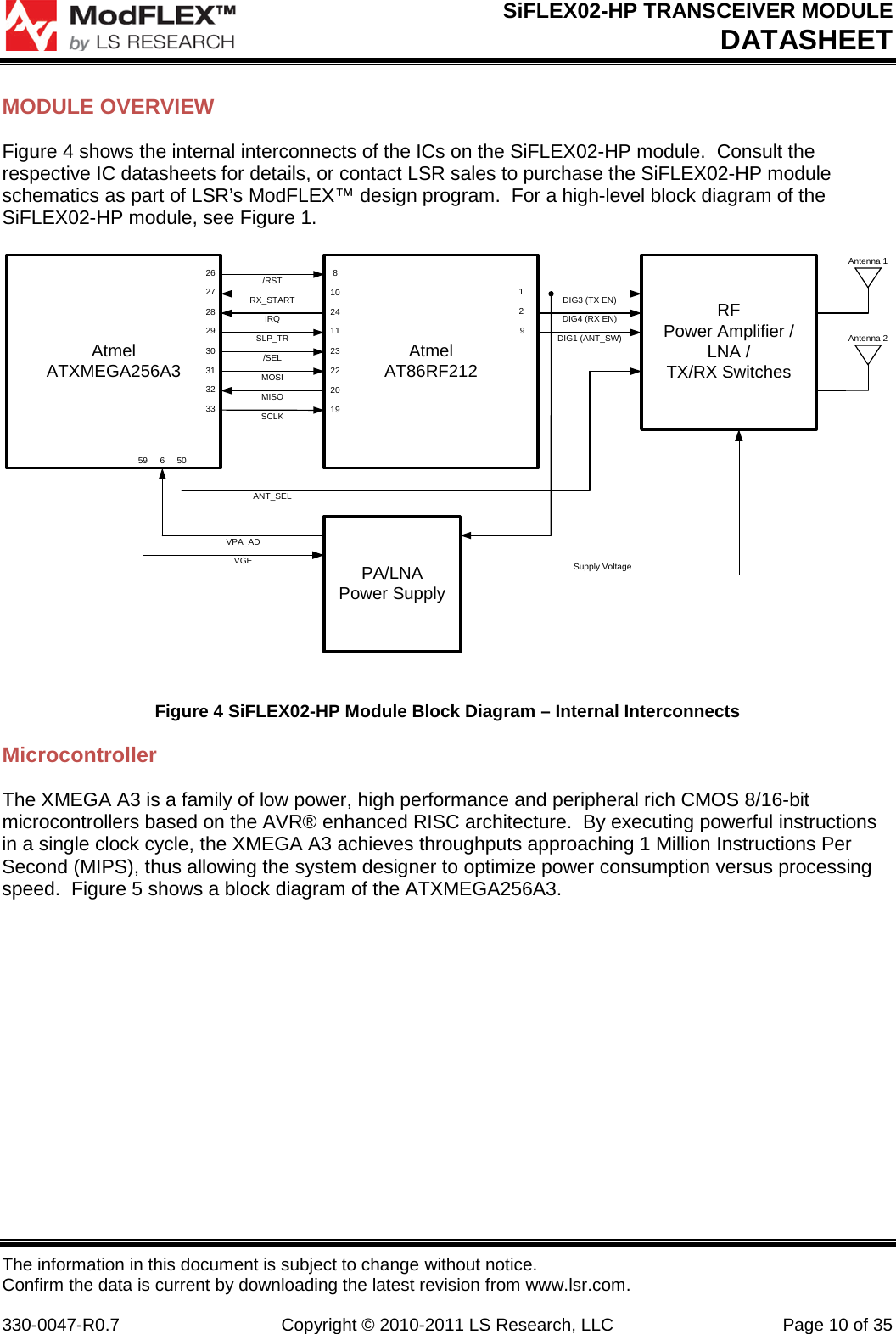
![SiFLEX02-HP TRANSCEIVER MODULE DATASHEET The information in this document is subject to change without notice. Confirm the data is current by downloading the latest revision from www.lsr.com. 330-0047-R0.7 Copyright © 2010-2011 LS Research, LLC Page 13 of 35 Figure 6 AT86RF212 Block Diagram RF Front End (Power Amplifier and LNA) The SiFLEX02-HP module contains a high performance RF Front End, containing both a RF Power Amplifier as well as a LNA. It is capable of 650mW output power, providing miles of range in outdoor applications. The signals DIG3 and DIG4 from the RF212 radio are used for transmit enable (TXEN) and receive enable (RXEN) respectively. When transmitting the DIG3 signal will be high and DIG4 will be low, which is controlled by the RF212. When receiving DIG3 will be low and DIG4 is high. In order to configure this functionality, the PA_EXT_EN bit in register TRX_CTRL_1 (0x04) of the RF212 needs to be set as a one. In addition the bits PA_LT[1] and PA_LT[0] in register RF_CTRL_0 (0x16) should both be set to one to maximize the PA lead time to 8usec. When putting the module to sleep the PA_EXT_EN bit should be set as zero. Upon wakeup the PA_EXT_EN should be set back to one.](https://usermanual.wiki/Laird-Connectivity/SIFLEX2HP/User-Guide-1520639-Page-13.png)