Laird Connectivity SIFLEX2HP SiFLEX-02HP User Manual Revison v0 7
LS Research, LLC SiFLEX-02HP Users Manual Revison v0 7
Users Manual Revison v0.7
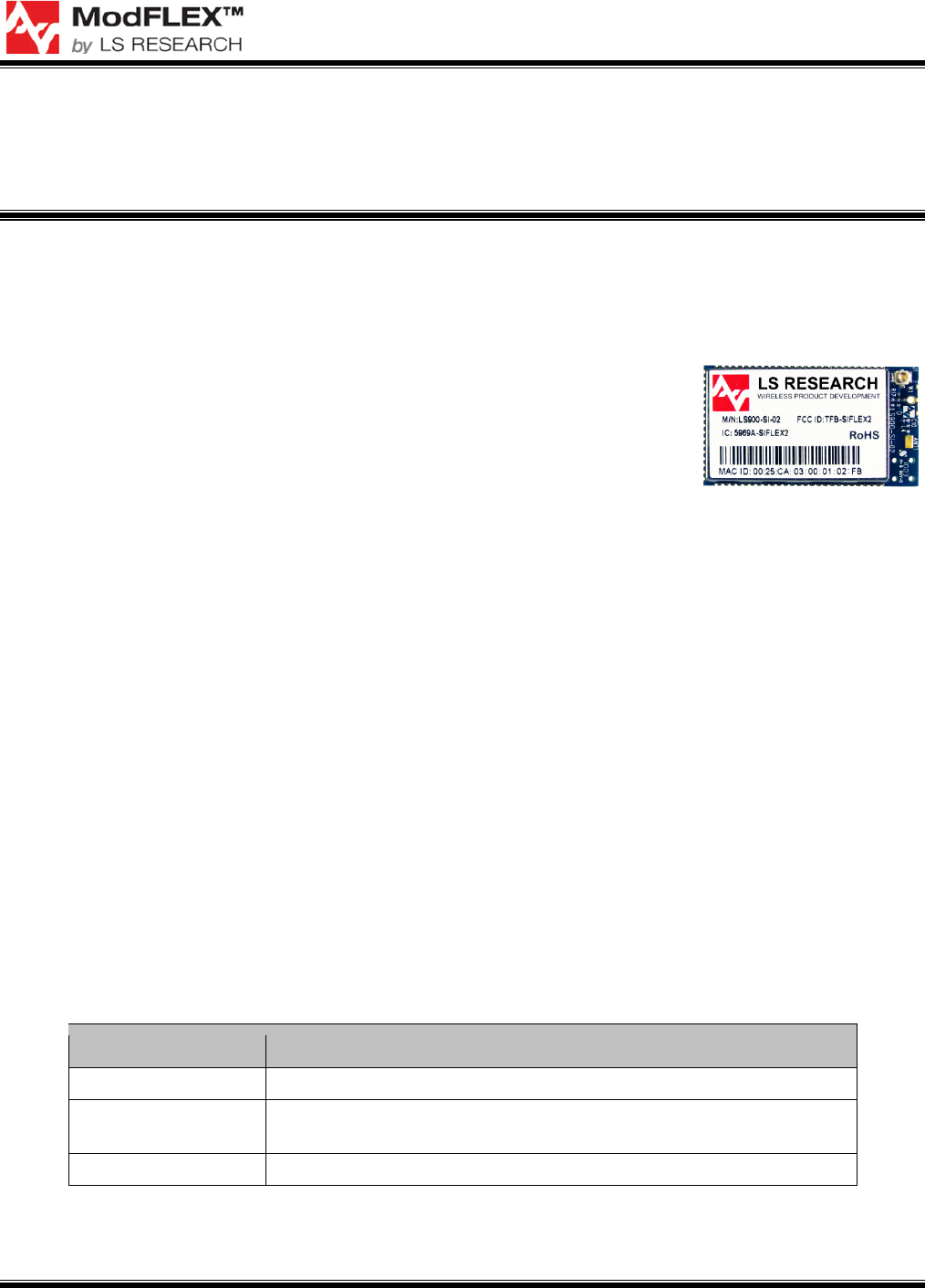
SiFLEX02-HP TRANSCEIVER MODULE
DATASHEET
The information in this document is subject to change without notice.
Confirm the data is current by downloading the latest revision from www.lsr.com.
330-0047-R0.7 Copyright © 2010-2011 LS Research, LLC Page 1 of 35
Integrated Transceiver Modules for ZigBee / 802.15.4 (900 MHz)
Development Kit Available
FEATURES
• 650mW output power
• Long range
• Up to 1Mbps RF data rate
• Miniature footprint: 0.9” x 1.63”
• Multiple antenna options
• Dual antennas
• Agency Approvals: FCC and IC
• Powerful Atmel 256k ATXMEGA256A3 with
802.15.4 MAC or ZigBee Stack
• LSR serial interface based on 802.15.4 MAC
• Low power operation
• RoHS compliant
• Streamlined development with LSR design
services.
• License options available to purchase
design or integrate design.
APPLICATIONS
• Security
• Lighting Control
• HVAC Control
• Sensor Networks
• Medical
• Industrial Automation
DESCRIPTION
The SiFLEX02-HP module is a high
performance 900MHz IEEE 802.15.4 radio
(AT86RF212 & RF
amplifier circuit) and
microcontroller
(ATXMEGA256A3)
in a cost effective,
pre-certified
footprint.
The module comes preloaded with the LSR
host serial interface running on top of the Atmel
802.15.4 MAC.
Full debug and programming capabilities are
included to develop custom applications. Easily
load the ZigBee stack or 802.15.4 MAC onto
the module and create your own network.
Need to get to market quickly? Not an expert in
802.15.4 or ZigBee? Need a custom antenna?
Would you like to own the design? Would you
like a custom design? Not quite sure what you
need? Do you need help with your host board?
LS Research Design Services will be happy to
develop custom hardware or software, integrate
the design, or license the design so you can
manufacture yourself. Contact us at
sales@lsr.com or call us at 262-375-4400.
ORDERING INFORMATION
Order Number
Description
450-0047
SiFLEX02-HP Module with u.fl connectors for external antennas
450-0049 SiFLEX02-HP Module with castellated RF traces for off board
antenna. Note: See Antenna Options section for more details.
SiFLEX02-HP Dev Kit
Table 1 Orderable SiFLEX02-HP Model Numbers
SiFLEX02-HP TRANSCEIVER MODULE
DATASHEET
The information in this document is subject to change without notice.
Confirm the data is current by downloading the latest revision from www.lsr.com.
330-0047-R0.7 Copyright © 2010-2011 LS Research, LLC Page 2 of 35
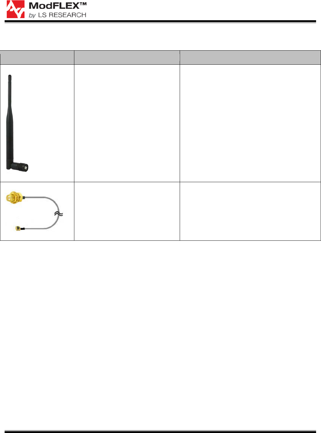
MODULE ACCESSORIES
Order Number
Description
001-0002 900 MHz Dipole Antenna with Reverse Polarity
SMA Connector
080-0001 u.fl to Reverse Polarity SMA Bulkhead Cable
105mm
SiFLEX02-HP TRANSCEIVER MODULE
DATASHEET
The information in this document is subject to change without notice.
Confirm the data is current by downloading the latest revision from www.lsr.com.
330-0047-R0.7 Copyright © 2010-2011 LS Research, LLC Page 3 of 35
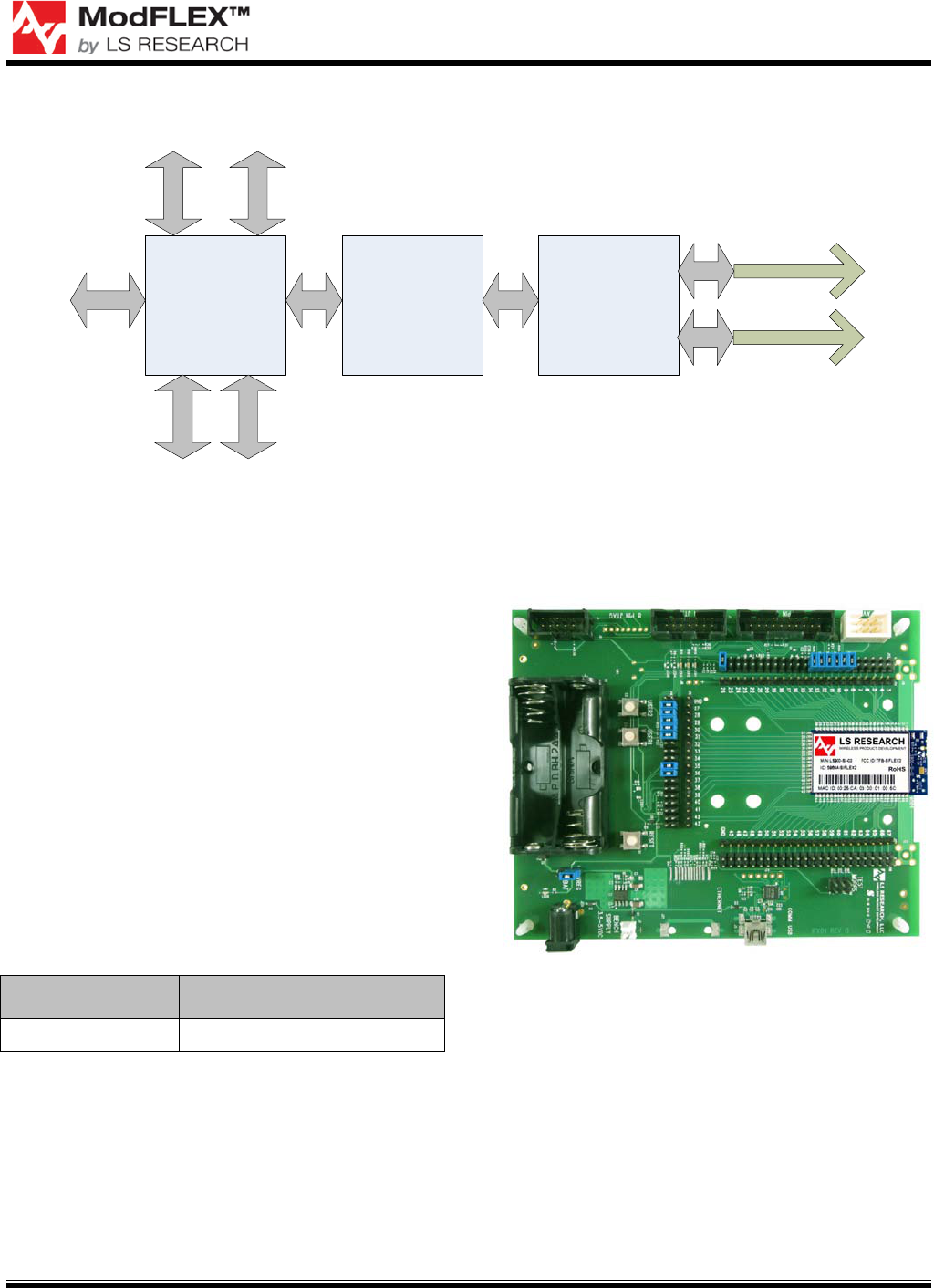
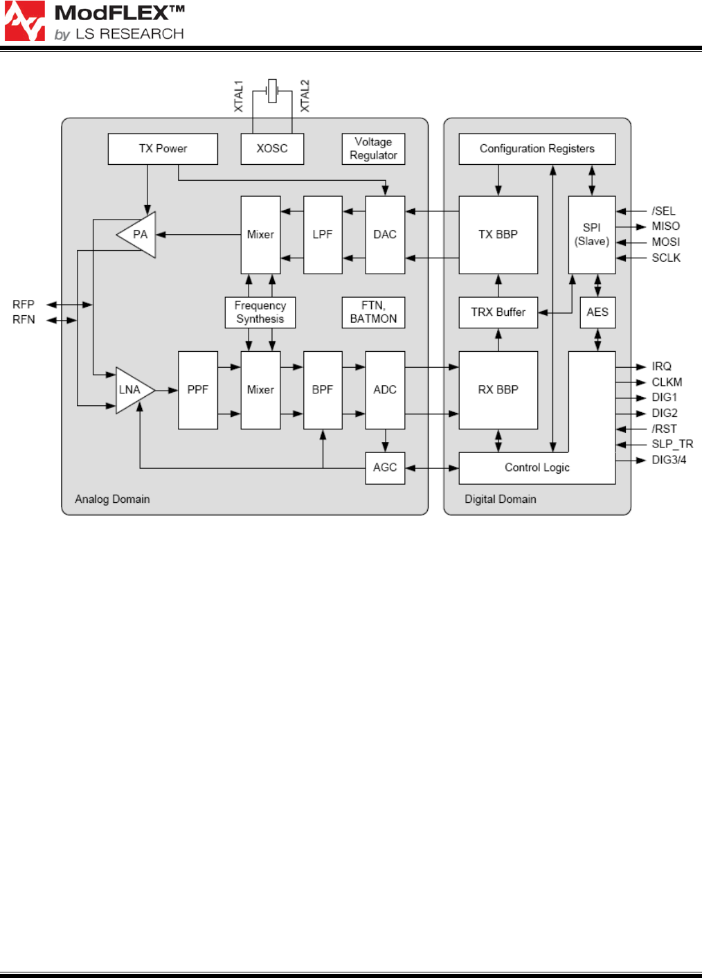
BLOCK DIAGRAM
ATXMEGA256A3
(Microcontroller) AT86RF212
(802.15.4 Radio)
RF Front End
Power Amplifier /
LNA
SPI
Antenna
Serial I/O
Analog
GPIO
PGM/DBG TMR/PWM
Antenna
Figure 1 SiFLEX02-HP Module Block Diagram – High-Level
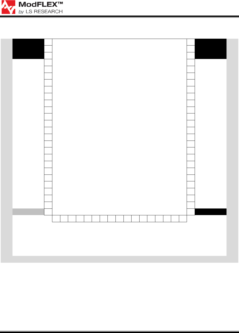
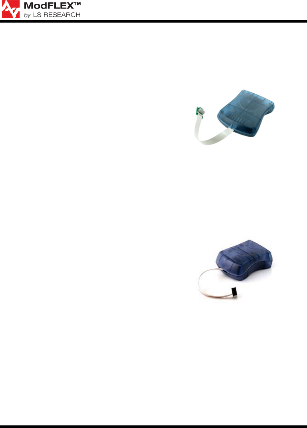
DEVELOPMENT KIT
The SiFLEX02-HP Development Kit can be
used out of the box to evaluate RF range
performance with the simple press of a button.
Users interested in further investigating the
performance and capabilities of the SiFLEX02-
HP Module can use the ModFLEXTM Test Tool.
This PC-based software can demonstrate just
how easy it is to send & receive data, collect
performance data, change channels, power
levels, or addresses using the LSR Serial Host
Protocol with another microcontroller.
More advanced users can use the development
board to create and debug their own software
for the SiFLEX02-HP module using the
802.15.4 MAC or ZigBee stack from Atmel.
Part Number
Description
SiFLEX02-HP Dev Kit
Figure 2 SiFLEX02-HP Development Board
Kit Contents
• ModFLEXTM Development Board with
SiFLEX02-HP Module with external
antennas (x2)
• USB Cable (x2)
• AA Batteries (x4)
• Software & Technical Information CD

SiFLEX02-HP TRANSCEIVER MODULE
DATASHEET
The information in this document is subject to change without notice.
Confirm the data is current by downloading the latest revision from www.lsr.com.
330-0047-R0.7 Copyright © 2010-2011 LS Research, LLC Page 4 of 35
TABLE OF CONTENTS
FEATURES .......................................................................................................................... 1
APPLICATIONS ................................................................................................................... 1
DESCRIPTION ..................................................................................................................... 1
ORDERING INFORMATION ................................................................................................ 1
MODULE ACCESSORIES ................................................................................................... 2
BLOCK DIAGRAM ............................................................................................................... 3
DEVELOPMENT KIT............................................................................................................ 3
Kit Contents ................................................................................................................................................. 3
MODULE PINOUT AND PIN DESCRIPTIONS .................................................................... 6
MODULE OVERVIEW ........................................................................................................ 10
Microcontroller .......................................................................................................................................... 10
Radio .......................................................................................................................................................... 12
RF Front End (Power Amplifier and LNA) ............................................................................................... 13
Antenna Options ....................................................................................................................................... 14
OPERATING MODES TRUTH TABLE .............................................................................. 15
MODES OF OPERATION .................................................................................................. 16
Host Microcontroller ................................................................................................................................. 16
Software Stacks ........................................................................................................................................ 16
DEVELOPMENT TOOLS ................................................................................................... 18
AVR Studio................................................................................................................................................. 18
Eclipse ........................................................................................................................................................ 18
WinAVR ...................................................................................................................................................... 18
AVR JTAGICE mkII .................................................................................................................................... 18
AVRISP mkII ............................................................................................................................................... 18
IAR Embedded Workbench for Atmel AVR ............................................................................................ 18
ELECTRICAL SPECIFICATIONS ...................................................................................... 19
Absolute Maximum Ratings ..................................................................................................................... 19
Recommended Operating Conditions .................................................................................................... 19
General Characteristics ............................................................................................................................ 20

SiFLEX02-HP TRANSCEIVER MODULE
DATASHEET
The information in this document is subject to change without notice.
Confirm the data is current by downloading the latest revision from www.lsr.com.
330-0047-R0.7 Copyright © 2010-2011 LS Research, LLC Page 5 of 35
RF Characteristics .................................................................................................................................... 21
SOLDERING RECOMMENDATIONS ................................................................................ 24
Recommended Reflow Profile for Lead Free Solder ............................................................................. 24
CLEANING ......................................................................................................................... 25
OPTICAL INSPECTION ..................................................................................................... 25
REWORK ........................................................................................................................... 25
SHIPPING, HANDLING, AND STORAGE ......................................................................... 25
Shipping ..................................................................................................................................................... 25
Handling ..................................................................................................................................................... 25
Moisture Sensitivity Level (MSL) ............................................................................................................. 25
Storage ....................................................................................................................................................... 25
Repeating Reflow Soldering .................................................................................................................... 25
AGENCY STATEMENTS ................................................................................................... 26
MECHANICAL DATA......................................................................................................... 32
PCB Footprint .................................................................................................. Error! Bookmark not defined.
General Module Dimensions .................................................................................................................... 32
COMPATIBILITY ................................................................................................................ 33
MODULE REVISION HISTORY ......................................................................................... 34
Rev 1.1 ........................................................................................................................................................ 34
CONTACTING LS RESEARCH ......................................................................................... 35
SiFLEX02-HP TRANSCEIVER MODULE
DATASHEET
The information in this document is subject to change without notice.
Confirm the data is current by downloading the latest revision from www.lsr.com.
330-0047-R0.7 Copyright © 2010-2011 LS Research, LLC Page 6 of 35
MODULE PINOUT AND PIN DESCRIPTIONS
MCU#
GND 1
SiFLEX02-HP
(Atmel ATXMEGA256A3)
69 GND MCU#
- GND 2 68 GND -
- GND 3 67 GND -
- NC 4 66 NC -
- NC 5 65 NC -
- VPA
6 64 NC -
- VPA
7 63 NC -
- NC 8 62 NC -
10 JTAG TMS 9 61 PC5 21
11 JTAG TDI 10 60 PC6 22
12 JTAG TCK 11 59 PC7 23
13 JTAG TDO 12 58 PC4 20
56 JTAG/PDI/JRST 13 57 PE0 36
57 nRESET 14 56 PE1 37
62 PA0 15 55 NC -
- NC 16 54 NC -
64 PA2 17 53 NC -
63 PA1 18 52 NC -
5 PA7 19 51 NC -
2 PA4 20 50 NC -
3 PA5 21 49 NC -
4 PA6 22 48 NC -
7 PB1 23 47 NC -
8 PB2 24 46 NC -
9 PB3 25 45 NC -
- VCC - 3V3DC 26 44 GND -
27 28 29 30 31 32 33 34 35 36 37 38 39 40 41 42 43
PF3
PF2
PF1
PF0
PE5
PE4
PE3
PE2
PC3/UART
TX
PC2/UART
RX
PC1
PC0
PF5
PF6
PF7
PA3
NC
MCU#
49 48 47 46 41 40 39 38 19 18 17 16 51 54 55 1 - MCU#
Figure 3 Module Pinout
SiFLEX02-HP TRANSCEIVER MODULE
DATASHEET
The information in this document is subject to change without notice.
Confirm the data is current by downloading the latest revision from www.lsr.com.
330-0047-R0.7 Copyright © 2010-2011 LS Research, LLC Page 7 of 35
Module
Pin
Name
MCU
Pin
Type Description
1
GND
N/A
GND
Ground
2
GND
N/A
GND
Ground
3
GND
N/A
GND
Ground
4
NC
N/A
NC
No Connect
5
NC
N/A
NC
No Connect
6 VPA N/A PWR RF Power Amplifier Supply Voltage
For 650mW output power provide 4.0VDC
For .5W output power provide 3.3VDC
7 VPA N/A PWR
RF Power Amplifier Supply Voltage
For 650mW output power provide 4.0VDC
For .5W output power provide 3.3VDC
8
NC
N/A
NC
No Connect
9
JTAG TMS
10
I/O
General-purpose digital I/O (PB4), Analog input, JTAG TMS
10
JTAG TDI
11
I/O
General-purpose digital I/O (PB5), Analog input, JTAG TDI
11
JTAG TCK
12
I/O
General-purpose digital I/O (PB6), Analog input, JTAG TCK
12
JTAG TDO
13
I/O
General-purpose digital I/O (PB7), Analog input, JTAG TDO
13
JTAG/PDI/JRST
56
I/O
PDI/PDI_DATA
14
nRESET
57
Input
RESET/PDI_CLOCK
15
PA0
62
I/O
General-purpose digital I/O, Analog input, Analog REF A
16
NC
N/A
NC
No Connect
17 PA2 64 I/O
General-purpose digital I/O, Analog input, Analog comparator
2
18 PA1 63 I/O General-purpose digital I/O, Analog input, Analog comparator
1
19 PA7 5 I/O
General-purpose digital I/O, Analog input, Analog comparator
output
20
PA4
2
I/O
General-purpose digital I/O, Analog input
21
PA5
3
I/O
General-purpose digital I/O, Analog input
22
PA6
4
I/O
General-purpose digital I/O, Analog input
23
PB1
7
I/O
General-purpose digital I/O, Analog input
24
PB2
8
I/O
General-purpose digital I/O, Analog input
25
PB3
9
I/O
General-purpose digital I/O, Analog input
26
VCC - 3V3DC
VCC
VCC
Supply Voltage
27
PF3
49
I/O
General-purpose digital I/O, Output Compare, UART Tx
28
PF2
48
I/O
General-purpose digital I/O, Output Compare, UART Rx

SiFLEX02-HP TRANSCEIVER MODULE
DATASHEET
The information in this document is subject to change without notice.
Confirm the data is current by downloading the latest revision from www.lsr.com.
330-0047-R0.7 Copyright © 2010-2011 LS Research, LLC Page 8 of 35
Module
Pin
Name
MCU
Pin
Type Description
29
PF1
47
I/O
General-purpose digital I/O, Output Compare, UART XCK0
30
PF0
46
I/O
General-purpose digital I/O, Output Compare
31 PE5 41 I/O General-purpose digital I/O, Output Compare, UART XCK1,
SPI MOSI
32
PE4
40
I/O
General-purpose digital I/O, Output Compare, SPI SS
33
PE3
39
I/O
General-purpose digital I/O, Output Compare, UART Tx
34
PE2
38
I/O
General-purpose digital I/O, Output Compare, UART Rx
35
PC3, UART TX
19
I/O
General-purpose digital I/O, Output Compare, UART Tx
36
PC2, UART RX
18
I/O
General-purpose digital I/O, Output Compare, UART Rx
37
PC1
17
I/O
General-purpose digital I/O, Output Compare, IIC SCL
38
PC0
16
I/O
General-purpose digital I/O, Output Compare, IIC SDA
39
PF5
51
I/O
General-purpose digital I/O
40
PF6
54
I/O
General-purpose digital I/O
41
PF7
55
I/O
General-purpose digital I/O
42
PA3
1
I/O
General-purpose digital I/O, Analog input
43
NC
N/A
NC
No Connect
44
GND
N/A
GND
Ground
45
NC
N/A
NC
No Connect
46
NC
N/A
NC
No Connect
47
NC
N/A
NC
No Connect
48
NC
N/A
NC
No Connect
49
NC
N/A
NC
No Connect
50
NC
N/A
NC
No Connect
51
NC
N/A
NC
No Connect
52
NC
N/A
NC
No Connect
53
NC
N/A
NC
No Connect
54
NC
N/A
NC
No Connect
55
NC
N/A
NC
No Connect
56
PE1
37
I/O
General-purpose digital I/O, Output Compare, IIC SCL
57
PE0
36
I/O
General-purpose digital I/O, Output Compare, IIC SDA
58
PC4
20
I/O
General-purpose digital I/O, Output Compare, SPI SS
59 PC7 23 I/O General-purpose digital I/O, Output Compare, UART Tx, SPI
SCK
SiFLEX02-HP TRANSCEIVER MODULE
DATASHEET
The information in this document is subject to change without notice.
Confirm the data is current by downloading the latest revision from www.lsr.com.
330-0047-R0.7 Copyright © 2010-2011 LS Research, LLC Page 9 of 35
Module
Pin
Name
MCU
Pin
Type Description
60 PC6 22 I/O
General-purpose digital I/O, Output Compare, UART Rx, SPI
MISO
61 PC5 21 I/O
General-purpose digital I/O, Output Compare, UART XCK1,
SPI MOSI
62
NC
N/A
NC
No Connect
63
NC
N/A
NC
No Connect
64
NC
N/A
NC
No Connect
65
NC
N/A
NC
No Connect
66
NC
N/A
NC
No Connect
67
GND
N/A
GND
Ground
68
GND
N/A
GND
Ground
69
GND
N/A
GND
Ground
Table 2 SiFLEX02-HP Module Pin Descriptions
SiFLEX02-HP TRANSCEIVER MODULE
DATASHEET
The information in this document is subject to change without notice.
Confirm the data is current by downloading the latest revision from www.lsr.com.
330-0047-R0.7 Copyright © 2010-2011 LS Research, LLC Page 10 of 35
MODULE OVERVIEW
Figure 4 shows the internal interconnects of the ICs on the SiFLEX02-HP module. Consult the
respective IC datasheets for details, or contact LSR sales to purchase the SiFLEX02-HP module
schematics as part of LSR’s ModFLEX™ design program. For a high-level block diagram of the
SiFLEX02-HP module, see Figure 1.
Atmel
ATXMEGA256A3
/RST
RX_START
/SEL
MOSI
MISO
SCLK
SLP_TR
IRQ
DIG3 (TX EN)
DIG4 (RX EN)
RF
Power Amplifier /
LNA /
TX/RX Switches
PA/LNA
Power Supply
26
27
28
29
30
31
32
33
Atmel
AT86RF212
8
10
24
11
23
22
20
19
1
2
DIG1 (ANT_SW)
9
50
ANT_SEL
VPA_AD
6
Antenna 1
Antenna 2
Supply Voltage
59
VGE
Figure 4 SiFLEX02-HP Module Block Diagram – Internal Interconnects
Microcontroller
The XMEGA A3 is a family of low power, high performance and peripheral rich CMOS 8/16-bit
microcontrollers based on the AVR® enhanced RISC architecture. By executing powerful instructions
in a single clock cycle, the XMEGA A3 achieves throughputs approaching 1 Million Instructions Per
Second (MIPS), thus allowing the system designer to optimize power consumption versus processing
speed. Figure 5 shows a block diagram of the ATXMEGA256A3.
SiFLEX02-HP TRANSCEIVER MODULE
DATASHEET
The information in this document is subject to change without notice.
Confirm the data is current by downloading the latest revision from www.lsr.com.
330-0047-R0.7 Copyright © 2010-2011 LS Research, LLC Page 11 of 35
Figure 5 ATXMEGA256A3 Block Diagram
The AVR CPU combines a rich instruction set with 32 general purpose working registers. All the 32
registers are directly connected to the Arithmetic Logic Unit (ALU), allowing two independent registers
to be accessed in one single instruction, executed in one clock cycle. The resulting architecture is
more code efficient while achieving throughputs many times faster than conventional single-
accumulator or CISC based microcontrollers.

SiFLEX02-HP TRANSCEIVER MODULE
DATASHEET
The information in this document is subject to change without notice.
Confirm the data is current by downloading the latest revision from www.lsr.com.
330-0047-R0.7 Copyright © 2010-2011 LS Research, LLC Page 12 of 35
The XMEGA A3 devices have five software selectable power saving modes. The Idle mode stops the
CPU while allowing the SRAM, DMA Controller, Event System, Interrupt Controller and all peripherals
to continue functioning. The Power-down mode saves the SRAM and register contents but stops the
oscillators, disabling all other functions until the next TWI or pin-change interrupt, or Reset. In Power-
save mode, the asynchronous Real Time Counter continues to run, allowing the application to maintain
a timer base while the rest of the device is sleeping. In Standby mode, the Crystal/Resonator Oscillator
is kept running while the rest of the device is sleeping. This allows very fast start-up from external
crystal combined with low power consumption. In Extended Standby mode, both the main Oscillator
and the Asynchronous Timer continue to run. To further reduce power consumption, the peripheral
clock for each individual peripheral can optionally be stopped in Active mode and Idle sleep mode.
Radio
The AT86RF212 is a low-power, low-voltage 900 MHz transceiver specially designed for low-cost IEEE
802.15.4, ZigBee™, and high data rate ISM applications. For the sub-1 GHz bands, it supports a low
data rate of 40kbps of the IEEE 802.15.4-2003 standard and provides an optional data rate 250kbps
using O-QPSK, according to IEEE 802.15.4-2006. Furthermore hardware accelerators improve overall
system power efficiency and timing.
The receiver path is based on a low-IF architecture. After channel filtering and down conversion the
low-IF signal is sampled and applied to the digital signal processing part. Communication between
transmitter and receiver is based on direct sequence spread spectrum with different modulation
schemes and spreading codes. The AT86RF212 supports the IEEE 802.15.4-2006 standard
mandatory BPSK modulation and optional O-QPSK modulation in the 900 MHz band. For applications
not necessarily targeting IEEE compliant networks the radio transceiver supports proprietary High Data
Rate Modes based on O-QPSK.
The AT86RF212 features hardware supported 128 bit security operation. The standalone AES
encryption/decryption engine can be accessed in parallel to all PHY operational modes. Configuration
of the AT86RF212, reading, and writing of data memory as well as the AES hardware engine are
controlled by the SPI interface and additional control signals.
SiFLEX02-HP TRANSCEIVER MODULE
DATASHEET
The information in this document is subject to change without notice.
Confirm the data is current by downloading the latest revision from www.lsr.com.
330-0047-R0.7 Copyright © 2010-2011 LS Research, LLC Page 13 of 35
Figure 6 AT86RF212 Block Diagram
RF Front End (Power Amplifier and LNA)
The SiFLEX02-HP module contains a high performance RF Front End, containing both a RF Power
Amplifier as well as a LNA. It is capable of 650mW output power, providing miles of range in outdoor
applications.
The signals DIG3 and DIG4 from the RF212 radio are used for transmit enable (TXEN) and receive
enable (RXEN) respectively. When transmitting the DIG3 signal will be high and DIG4 will be low,
which is controlled by the RF212. When receiving DIG3 will be low and DIG4 is high. In order to
configure this functionality, the PA_EXT_EN bit in register TRX_CTRL_1 (0x04) of the RF212 needs to
be set as a one. In addition the bits PA_LT[1] and PA_LT[0] in register RF_CTRL_0 (0x16) should both
be set to one to maximize the PA lead time to 8usec.
When putting the module to sleep the PA_EXT_EN bit should be set as zero. Upon wakeup the
PA_EXT_EN should be set back to one.

SiFLEX02-HP TRANSCEIVER MODULE
DATASHEET
The information in this document is subject to change without notice.
Confirm the data is current by downloading the latest revision from www.lsr.com.
330-0047-R0.7 Copyright © 2010-2011 LS Research, LLC Page 14 of 35
Antenna Options
The SiFLEX02-HP module includes multiple antenna options. The module’s regulatory certification has
been completed with the following antenna:
• LS Research 001-0002 900 MHz Dipole Antenna with Reverse Polarity SMA Connector and LS
Research 080-0001 u.fl to Reverse Polarity SMA Bulkhead Cable (105mm in length)
The SiFLEX02-HP RF castellations for off board antennas are not covered in the modular certification.
If a host board is designed that will utilize off board antennas via the RF castellated antenna
connections, an additional certification will be required. LS Research is equipped with a certification lab
and can assist in getting this done at a very reasonable cost in a short period of time.
An adequate ground plane is necessary to provide good efficiency. The ground plane of the host board
on which the module is mounted increases the effective antenna ground plane size and improves the
antenna performance.
The environment the module is placed in will dictate the range performance The non-ideal
characteristics of the environment will result in the transmitted signal being reflected, diffracted, and
scattered. All of these factors randomly combine to create extremely complex scenarios that will affect
the link range in various ways.
It is also best to keep some clearance between the antennas and nearby objects. This includes how
the module is mounted in the product enclosure. Unless the items on the following list of
recommendations are met, the radiation pattern can be heavily distorted.
Whichever antenna is used, it is best to keep a few things in mind when determining its location.
• Never place ground plane or copper trace routing underneath the antenna.
• LSR recommends keeping metal objects as far away from the antenna as possible. At a very minimum
keep the antenna at least 5 cm from any metallic objects, components, or wiring. The farther the antenna
is placed from these interferers, the less the radiation pattern and gain will be perturbed.
• Do not embed the antenna in a metallic or metalized plastic enclosure.
• If located within a plastic enclosure, keep the enclosure at least 1 cm from the antenna.
SiFLEX02-HP TRANSCEIVER MODULE
DATASHEET
The information in this document is subject to change without notice.
Confirm the data is current by downloading the latest revision from www.lsr.com.
330-0047-R0.7 Copyright © 2010-2011 LS Research, LLC Page 15 of 35
OPERATING MODES TRUTH TABLE
Mode
VGE
LNA_EN
ANT_SW
ANT_SEL
Sleep
0
0
0
0
Transmit – Ant J1
1
0
1
0
Receive with LNA Disabled – Ant J1
1
0
0
1 (J1 RX)
Receive with LNA Disabled – Ant J2
1
0
0
0 (J2 RX)
Receive with LNA Enabled – Ant J1
1
1
0
1 (J1 RX)
Receive with LNA Enabled – Ant J2
1
1
0
0 (J2 RX)
Table 3 Operating Modes Truth Table
SiFLEX02-HP TRANSCEIVER MODULE
DATASHEET
The information in this document is subject to change without notice.
Confirm the data is current by downloading the latest revision from www.lsr.com.
330-0047-R0.7 Copyright © 2010-2011 LS Research, LLC Page 16 of 35
MODES OF OPERATION
• With a host microcontroller
• With the Atmel 802.15.4 MAC
• With the Atmel ZigBee stack
Host Microcontroller
Si-FLEX Module on
Evaluation Board
UART
PC
LSR Test Tool
Software
Si-FLEX Module on
Your Board
Your Microcontroller
(Host) of Choice UART
-OR-
Figure 7 Host Microcontroller Modes of
Operation
Out of the box the SiFLEX02-HP module
contains an 802.15.4 based application that
uses a host serial processor. This allows
features of the module to be explored with the
LSR PC based test tool, or controlled with a
host microcontroller. The advantage of this
method is simplicity; all major features of using
the radio are simplified into a simple serial
message, taking the burden of becoming a
radio expert off the developer.
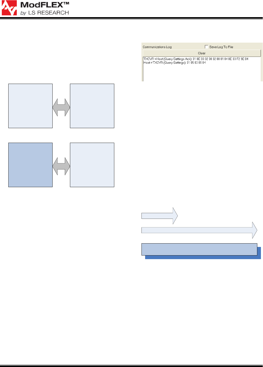
Use the Communications Log in the
ModFLEX™ Test Tool software and serial host
protocol documents to see the messages in
action. It will help you become familiar with the
serial commands and how to implement them
on your own microcontroller.
Figure 8 ModFLEX™ Test Tool Communications
Log
Some examples of serial commands that can
be used with the SiFLEX02-HP Module:
• Set/Query RF channel
• Set/Query RF power
• Set/Query device address
• Transmit RF data or notification RF data
received
• Go to Sleep
Software Stacks
There are two software stacks provided by
Atmel to streamline development:
MAC (802.15.4)
Atmel ZigBee Stack
Overall Complexity and Development Effort
Figure 9 SiFLEX02-HP Compatible Stacks
802.15.4 MAC
• Use for applications requiring point-to-
point or star network topology.
• Advantages: Quick learning curve,
minimize software development, easy to
deploy in the field
• Disadvantages: No mesh networking
SiFLEX02-HP TRANSCEIVER MODULE
DATASHEET
The information in this document is subject to change without notice.
Confirm the data is current by downloading the latest revision from www.lsr.com.
330-0047-R0.7 Copyright © 2010-2011 LS Research, LLC Page 17 of 35
802.15.4 MAC
(To Tx/Rx RF data)
Application Software
(to control switches,
LED’s, serial ports
and so on)
Software
Interface
Figure 10 SiFLEX02-HP with 802.15.4 MAC
Atmel ZigBee Stack
• Use when mesh networking is required.
• Advantages: Covers a large area with a
ZigBee network.
• Disadvantages: Large learning curve, more
software development, complexity
Application Software
(to control switches,
LED’s, serial ports
and so on)
Software
Interface ZigBee Stack
(To Tx/Rx RF data)
Figure 11 SiFLEX02-HP with Atmel ZigBee Stack
SiFLEX02-HP TRANSCEIVER MODULE
DATASHEET
The information in this document is subject to change without notice.
Confirm the data is current by downloading the latest revision from www.lsr.com.
330-0047-R0.7 Copyright © 2010-2011 LS Research, LLC Page 18 of 35
DEVELOPMENT TOOLS
AVR Studio
AVR Studio® is an Integrated Development
Environment (IDE) for writing and debugging
AVR® applications in Windows®
9x/NT/2000/XP/Vista(32- and 64-bit)
environments. AVR Studio 4 includes an
assembler, simulator, and in-circuit debugger.
AVR Studio is the Integrated Development
Environment (IDE) developed by Atmel for
writing and debugging Atmel AVR applications.
Eclipse
Eclipse is an IDE for C/C++ developers.
The Eclipse IDE requires a Java Runtime
Environment (JRE) be installed on your
machine to run. While it can run using a Java
1.4 JRE, a Java5 JRE (minimum) is
recommended.
See the SiFLEX02-HP User’s Guide for detailed
instructions for installing Eclipse and integrating
it with AVR Studio and WinAVR.
WinAVR
WinAVR is a suite of executable, open source
software development tools for the Atmel AVR
series of RISC microprocessors hosted on the
Windows platform. It includes the GNU GCC
compiler for C/C++.
WinAVR contains all the tools for developing on
AVR family microcontrollers from Atmel. This
includes avr-gcc (compiler), avrdude
(programmer), avr-gdb (debugger), and more.
AVR JTAGICE mkII
Custom firmware development can be done on
the SiFLEX02-HP module using development
tools available through Atmel. Shown in Figure
12, a JTAGICE mkII interface is required. It
plugs into the ModFLEX™ Development Board,
and can easily be adapted to other hardware.
See the Atmel website for more information and
ordering options.
Figure 12 AVR JTAGICE mkII
AVRISP mkII
Another option for in-circuit programming is the
AVRISP mkII from Atmel, Figure 13. The
AVRISP mkII combined with AVR Studio® can
program new AVR 8-bit RISC microcontrollers
with ISP Interface.
Figure 13 AVRISP mkII
IAR Embedded Workbench for Atmel
AVR
Another option is IAR Embedded Workbench
for Atmel AVR. IAR Embedded Workbench for
AVR is an integrated development environment
for building and debugging embedded
applications. Visit the IAR Systems website for
additional information.
SiFLEX02-HP TRANSCEIVER MODULE
DATASHEET
The information in this document is subject to change without notice.
Confirm the data is current by downloading the latest revision from www.lsr.com.
330-0047-R0.7 Copyright © 2010-2011 LS Research, LLC Page 19 of 35
ELECTRICAL SPECIFICATIONS
The majority of these characteristics are based on the use of the Atmel IEEE 802.15.4 MAC loaded
with the generic application firmware written by LSR. Custom firmware may require these values to be
re-characterized by the customer.
Absolute Maximum Ratings
Rating
Min
Max
Unit
Power supply voltage (VCC)
0
3.6
V
Power Amplifier supply voltage (VPA)
0
4.5
V
Voltage on any pin with respect to ground
-0.3
Vcc + 0.3
V
RF input power
+10
dBm
Operating temperature range
-40
+85
ºC
Storage temperature
-50
+150
ºC
Table 4 Absolute Maximum Ratings1
Recommended Operating Conditions
Characteristic
Min
Typ
Max
Unit
Power supply voltage (VCC)
2.5
3.3
3.50
Vdc
Power Amplifier supply voltage (VPA)
3.0
4.0
4.25
Vdc
Ambient temperature range
-40
25
85
ºC
Table 5 Recommended Operating Conditions
Module will NOT transmit, if VPA > 4.25V.
1 Under no circumstances should exceeding the maximum ratings specified in the Absolute Maximum Ratings
section be allowed. Stressing the module beyond these limits may result permanent damage to the module that
is not covered by the warranty.
SiFLEX02-HP TRANSCEIVER MODULE
DATASHEET
The information in this document is subject to change without notice.
Confirm the data is current by downloading the latest revision from www.lsr.com.
330-0047-R0.7 Copyright © 2010-2011 LS Research, LLC Page 20 of 35
General Characteristics
Parameter
Min
Typ
Max
Unit
RF frequency range (Note 1, 2)
906
924
MHz
RF data rate
40
1000
kbps
Host data rate
1.2
19.2
921.6
kbps
Flash memory
256
kBytes
RAM
16
kBytes
EEPROM
4
kBytes
Table 6 General Characteristics
Note 1: The frequency range needs to be restricted to 915 to 924 MHz (channels 6-10) to meet
Australian/New Zealand standards.
Note 2:Due to the band pass filter, receiver sensitivity is reduced by approximately 1dB on channels 1,
2, 8, 9, and 10 (906MHz, 908MHz, 920MHz, 922MHz, and 924MHz). This improves receiver
performance in the presence of interferers on channels 3, 4, 5, 6, and 7 (910MHz, 912MHz,
914MHz, 916MHz, and 918MHz).
Power Consumption
(TA = 25°C, VCC = 3.3V, VPA = 4.0V, fc = 906-924MHz, Rload = 50Ω)
Parameter
Test Conditions
Min
Typ
Max
Unit
Transmit mode - VPA
Maximum power step
450
600
mA
Transmit mode - VCC
50
mA
Receive mode - VPA
1
uA
Receive mode - VCC
27
39
48
mA
Sleep mode - VPA
1
µA
Sleep mode - VCC
2
5
uA
Table 7 Power Consumption
DC Characteristics – General Purpose I/O
Parameter
Test Conditions
Min
Typ
Max
Unit
Logic input low
-0.3
0.2 * Vcc
V
Logic input high
0.8 * Vcc
Vcc + 0.3
V
Logic output low
I
OUT
= 15mA
Vcc = 3.3V
0.4 V
Logic output high
I
OUT
= -8mA
Vcc = 3.3V
2.9 V
Table 8 DC Characteristics – General Purpose I/O
SiFLEX02-HP TRANSCEIVER MODULE
DATASHEET
The information in this document is subject to change without notice.
Confirm the data is current by downloading the latest revision from www.lsr.com.
330-0047-R0.7 Copyright © 2010-2011 LS Research, LLC Page 21 of 35
RF Characteristics
Transmitter Characteristics
(TA = 25°C, VCC = 3.3V, VPA = 4.0V, fc = 906-924 MHz)
Parameter
Test Conditions
Min
Typ
Max
Unit
Nominal max output power
(40kbps)
(Notes: 1, 2) 26 27 29 dBm
Nominal max output power
(250kbps and higher)
(Notes: 1, 2) 27 28 29 dBm
Programmable output power range
22 Steps
15
28
dBm
Harmonics (2fo)
-50
dBm
Harmonics (3fo)
-55
dBm
Error vector magnitude
10
35
% rms
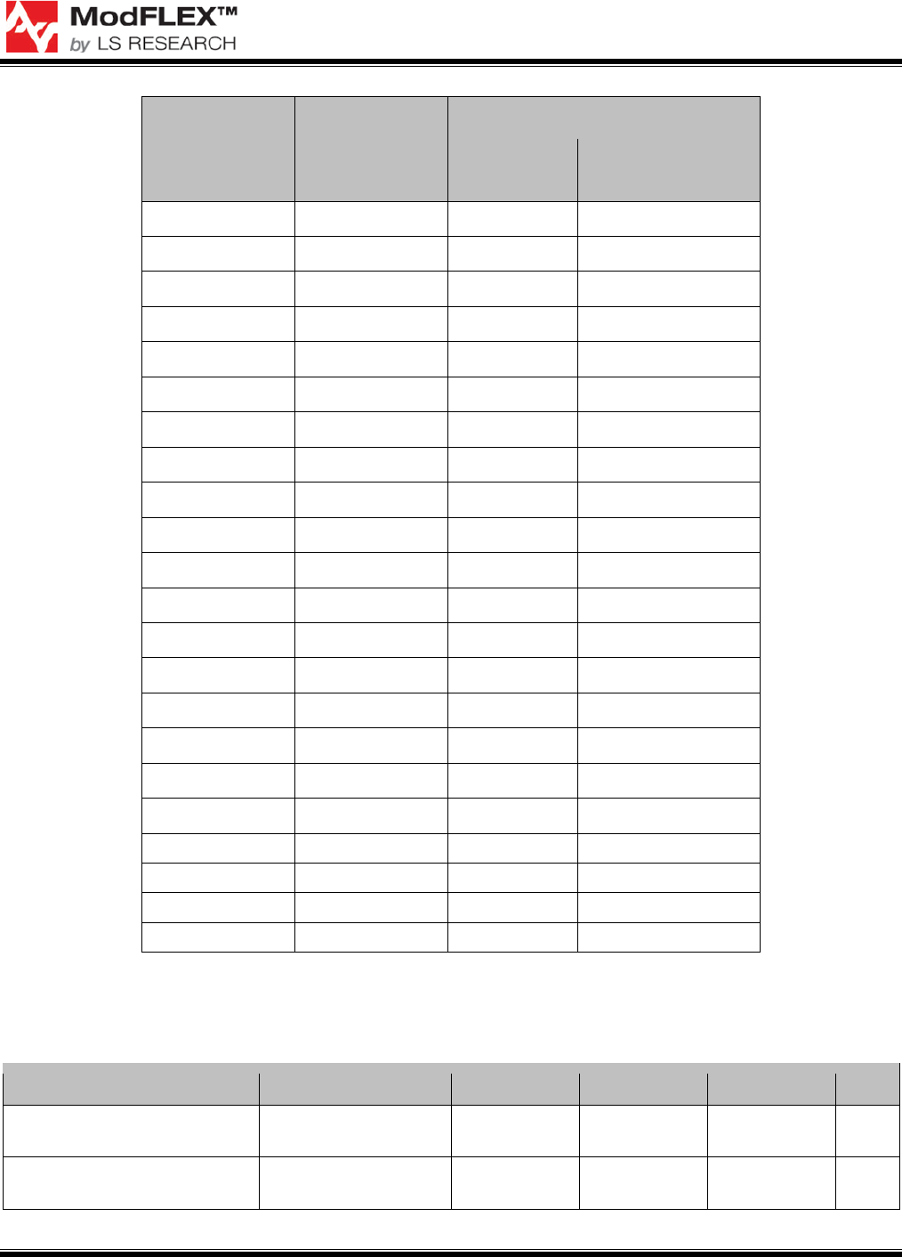
Table 9 Transmitter RF Characteristics
Note 1: In accordance with FCC Part 15.247(e) and RSS 210 A8.2(b), the peak power spectral density
should not exceed +8 dBm in any 3 KHz band.
Note 2: In accordance with Australian/New Zealand 4268 : 2008, the peak power spectral density
should not exceed +14dBm in any 3 KHz band in the 915 to 928 MHz frequency band.
SiFLEX02-HP TRANSCEIVER MODULE
DATASHEET
The information in this document is subject to change without notice.
Confirm the data is current by downloading the latest revision from www.lsr.com.
330-0047-R0.7 Copyright © 2010-2011 LS Research, LLC Page 22 of 35
Host Protocol
RF Power
Level
AT86RF212
PHY_TX_PWR
Register Value
BPSK into 50 ohms at u.fl
RF Output
Power (dBm)
Typical Current
Consumption (mA)
21
0x0C
28
466
20
0x0B
28 455
19 0x0A 28 443
18
0x09
28
426
17
0x08
27
393
16
0x07
26 365
15
0x06
26
346
14
0x05
26
338
13
0x04
25 319
12
0x03
25 304
11
0x02
24
281
10
0x23
24
277
9
0x22
22 254
8
0x42
22 236
7
0x41
21
219
6
0x61
21
207
5
0x60
20 198
4 0x83 19 188
3
0x82
18
181
2
0x81
17
176
1
0xA1
16
172
0
0xC0
15
170
Table 10 RF Power Settings
Receiver Characteristics
(TA = 25°C, VCC = 3.3V, VPA = 4.0V, fc = 906-924 MHz)
Parameter
Test Conditions
Min
Typ
Max
Unit
Receiver Sensitivity
@ 1% PER
BPSK 40kbit/s < -104 dBm
Saturation Level
@ 1% PER
BPSK 40kbit/s -2 dBm
Table 11 Receiver RF Characteristics

SiFLEX02-HP TRANSCEIVER MODULE
DATASHEET
The information in this document is subject to change without notice.
Confirm the data is current by downloading the latest revision from www.lsr.com.
330-0047-R0.7 Copyright © 2010-2011 LS Research, LLC Page 23 of 35
For additional details regarding the electrical specifications, refer to the ATXMEGA256A3 and
AT86RF212 datasheets on the Atmel website.
SiFLEX02-HP TRANSCEIVER MODULE
DATASHEET
The information in this document is subject to change without notice.
Confirm the data is current by downloading the latest revision from www.lsr.com.
330-0047-R0.7 Copyright © 2010-2011 LS Research, LLC Page 24 of 35
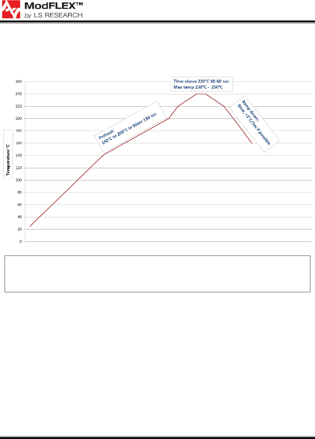
SOLDERING RECOMMENDATIONS
Recommended Reflow Profile for Lead Free Solder
Note: The quality of solder joints on the castellations (‘half vias’) where they contact the
host board should meet the appropriate IPC Specification. See IPC-A-610-D Acceptability
of Electronic Assemblies, section 8.2.4 Castellated Terminations.”

SiFLEX02-HP TRANSCEIVER MODULE
DATASHEET
The information in this document is subject to change without notice.
Confirm the data is current by downloading the latest revision from www.lsr.com.
330-0047-R0.7 Copyright © 2010-2011 LS Research, LLC Page 25 of 35
CLEANING
In general, cleaning the populated modules is
strongly discouraged. Residuals under the
module cannot be easily removed with any
cleaning process.
• Cleaning with water can lead to capillary
effects where water is absorbed into the gap
between the host board and the module.
The combination of soldering flux residuals
and encapsulated water could lead to short
circuits between neighboring pads. Water
could also damage any stickers or labels.
• Cleaning with alcohol or a similar organic
solvent will likely flood soldering flux
residuals into the RF shield, which is not
accessible for post-washing inspection. The
solvent could also damage any stickers or
labels.
• Ultrasonic cleaning could damage the
module permanently.
OPTICAL INSPECTION
After soldering the Module to the host board,
consider optical inspection to check the
following:
• Proper alignment and centering of the
module over the pads.
• Proper solder joints on all pads.
• Excessive solder or contacts to neighboring
pads, or vias.
REWORK
The SiFLEX02-HP module can be unsoldered
from the host board. Use of a hot air rework
tool and hot plate for pre-heating from
underneath is recommended. Avoid
overheating.
Never attempt a rework on the
module itself, e.g. replacing
individual components. Such actions
will terminate warranty coverage.
SHIPPING, HANDLING, AND STORAGE
Shipping
Bulk orders of the SiFLEX02-HP modules are
delivered in trays of 50.
Handling
The SiFLEX02-HP modules contain a highly
sensitive electronic circuitry. Handling without
proper ESD protection may destroy or damage
the module permanently. ESD protection may
destroy or damage the module permanently.
Moisture Sensitivity Level (MSL)
MSL 4, per J-STD-020
Devices not stored in a sealed bag with
desiccant pack should be baked.
After opening devices that will be subjected to
reflow must be mounted within 72 hours of
factory conditions (<30°C and 60% RH) or
stored at <10% RH.
Bake devices for 8 hours at 125°C.
Storage
Storage/shelf life in sealed bags is 12 months at
<40°C and <90% relative humidity.
Repeating Reflow Soldering
Only a single reflow soldering
process is encouraged for host
boards.

SiFLEX02-HP TRANSCEIVER MODULE
DATASHEET
The information in this document is subject to change without notice.
Confirm the data is current by downloading the latest revision from www.lsr.com.
330-0047-R0.7 Copyright © 2010-2011 LS Research, LLC Page 26 of 35
AGENCY STATEMENTS
Federal Communication Commission Interference Statement
This equipment has been tested and found to comply with the limits for a Class B digital device,
pursuant to Part 15 of the FCC Rules. These limits are designed to provide reasonable protection
against harmful interference in a residential installation. This equipment generates uses and can radiate
radio frequency energy and, if not installed and used in accordance with the instructions, may cause
harmful interference to radio communications. However, there is no guarantee that interference will not
occur in a particular installation. If this equipment does cause harmful interference to radio or television
reception, which can be determined by turning the equipment off and on, the user is encouraged to try
to correct the interference by one of the following measures:
• Reorient or relocate the receiving antenna.
• Increase the separation between the equipment and receiver.
• Connect the equipment into an outlet on a circuit different from that to which the receiver is
connected.
• Consult the dealer or an experienced radio/TV technician for help.
This device complies with Part 15 of the FCC Rules. Operation is subject to the following two
conditions: (1) This device may not cause harmful interference, and (2) this device must accept any
interference received, including interference that may cause undesired operation.
FCC CAUTION: Any changes or modifications not expressly approved by the party
responsible for compliance could void the user's authority to operate this equipment.

SiFLEX02-HP TRANSCEIVER MODULE
DATASHEET
The information in this document is subject to change without notice.
Confirm the data is current by downloading the latest revision from www.lsr.com.
330-0047-R0.7 Copyright © 2010-2011 LS Research, LLC Page 27 of 35
Industry Canada Statements
Operation is subject to the following two conditions: (1) this device may not cause interference, and (2)
this device must accept any interference, including interference that may cause undesired operation of
the device.
To reduce potential radio interference to other users, the antenna type and its gain should be so
chosen that the equivalent isotropically radiated power (e.i.r.p.) is not more than that permitted for
successful communication.
This device has been designed to operate with the antennas listed below, and having a maximum gain
of 2.0 dB. Antennas not included in this list or having a gain greater than 2.0 dB are strictly prohibited
for use with this device. The required antenna impedance is 50 ohms.
LS Research 001-0002 900 MHz Dipole Antenna with Reverse Polarity SMA Connector and LS
Research 080-0001 u.fl to Reverse Polarity SMA Bulkhead Cable (105mm in length)
Son fonctionnement est soumis aux deux conditions suivantes: (1) cet appareil ne peut pas provoquer
d'interférences et (2) cet appareil doit accepter toute interférence, y compris les interférences qui
peuvent causer un mauvais fonctionnement du dispositif.
Pour réduire le risque d'interférence aux autres utilisateurs, le type d'antenne et son gain doivent être
choisies de façon que la puissance isotrope rayonnée équivalente (e.i.r.p) ne dépasse pas celle admise
pour une communication réussie.
Cet appareil a été conçu pour fonctionner avec les antennes énumérées ci-dessous, et ayant un gain
maximum de 2,0 dB. Antennes pas inclus dans cette liste ou ayant un gain supérieur à 2,0 dB sont
strictement interdites pour une utilisation avec cet appareil. L'impédance d'antenne requise est de 50
ohms.
LS Research 001-0002 900 MHz Antenne dipôle avec inversion de polarité Connecteur
SMA et LS Research 080-0001 U.FL àinversion de polarité SMA traversée de câble (105 mm de
longueur)

SiFLEX02-HP TRANSCEIVER MODULE
DATASHEET
The information in this document is subject to change without notice.
Confirm the data is current by downloading the latest revision from www.lsr.com.
330-0047-R0.7 Copyright © 2010-2011 LS Research, LLC Page 28 of 35
OEM Responsibilities to comply with FCC and Industry Canada Regulations
The SiFLEX02-HP Module has been certified for integration into products only by OEM integrators
under the following conditions:
This device is granted for use in Mobile only configurations in which the antennas used for this
transmitter must be installed to provide a separation distance of at least 20cm from all person and not
be co-located with any other transmitters except in accordance with FCC and Industry Canada multi-
transmitter product procedures.
As long as the two conditions above are met, further transmitter testing will not be required. However,
the OEM integrator is still responsible for testing their end-product for any additional compliance
requirements required with this module installed (for example, digital device emissions, PC peripheral
requirements, etc.).
IMPORTANT NOTE: In the event that these conditions cannot be met (for certain
configurations or co-location with another transmitter), then the FCC and Industry
Canada authorizations are no longer considered valid and the FCC ID and IC Certification
Number cannot be used on the final product. In these circumstances, the OEM integrator
will be responsible for re-evaluating the end product (including the transmitter) and
obtaining a separate FCC and Industry Canada authorization.

SiFLEX02-HP TRANSCEIVER MODULE
DATASHEET
The information in this document is subject to change without notice.
Confirm the data is current by downloading the latest revision from www.lsr.com.
330-0047-R0.7 Copyright © 2010-2011 LS Research, LLC Page 29 of 35
Le module SiFLEX02-HP a été certifiée pour l'intégration dans les produits que par les intégrateurs
OEM dans les conditions suivantes:
Ce dispositif est accordé pour une utilisation dans des configurations mobiles seule dans
laquelle les antennes utilisées pour cet émetteur doit être installé pour fournir une distance
de séparation d'au moins 20cm de toute personne et ne pas être co-localisés
avec les autres émetteurs, sauf en conformité avec FCC et Industrie Canada, multi-
émetteur procedures produit.
Tant que les deux conditions précitées sont réunies, les tests de transmetteurs supplémentaires ne
seront pas tenus. Toutefois, l'intégrateur OEM est toujours responsable de tester leur produit final pour
toutes les exigences de conformité supplémentaires requis avec ce module installé (par exemple, les
émissions appareil numérique, les exigences de périphériques PC, etc.)
NOTE IMPORTANTE: Dans le cas où ces conditions ne peuvent être satisfaites (pour
certaines configurations ou de co-implantation avec un autre émetteur), puis la FCC et
Industrie autorisations Canada ne sont plus considérés comme valides et l'ID de la FCC
et IC numéro de certification ne peut pas être utilisé sur la produit final. Dans ces
circonstances, l'intégrateur OEM sera chargé de réévaluer le produit final (y compris
l'émetteur) et l'obtention d'un distincte de la FCC et Industrie Canada l'autorisation.

SiFLEX02-HP TRANSCEIVER MODULE
DATASHEET
The information in this document is subject to change without notice.
Confirm the data is current by downloading the latest revision from www.lsr.com.
330-0047-R0.7 Copyright © 2010-2011 LS Research, LLC Page 30 of 35
End Product Labelling
The SiFLEX02-HP Module is labeled with its own FCC ID and IC Certification Number. If the FCC ID
and IC Certification Number are not visible when the module is installed inside another device, then the
outside of the device into which the module is installed must also display a label referring to the
enclosed module. In that case, the final end product must be labeled in a visible area with the
following:
“Contains Transmitter Module FCC ID: TFB-SIFLEX2HP”
“Contains Transmitter Module IC: 5969A-SIFLEX2HP”
or
“Contains FCC ID: TFB-SIFLEX2HP”
“Contains IC: 5969A-SIFLEX2HP”
The OEM of the SiFLEX02-HP Module must only use the approved antenna(s) listed above, which
have been certified with this module.
The OEM integrator has to be aware not to provide information to the end user regarding how to install
or remove this RF module or change RF related parameters in the user manual of the end product.
The user manual for the end product must include the following information in a prominent
location:
This device is granted for use in Mobile only configurations in which the antennas used
for this transmitter must be installed to provide a separation distance of at least 20cm
from all person and not be co-located with any other transmitters except in accordance
with FCC and Industry Canada multi-transmitter product procedures.

SiFLEX02-HP TRANSCEIVER MODULE
DATASHEET
The information in this document is subject to change without notice.
Confirm the data is current by downloading the latest revision from www.lsr.com.
330-0047-R0.7 Copyright © 2010-2011 LS Research, LLC Page 31 of 35
Le SiFLEX02-HP Module est étiqueté avec sa propre ID de la FCC et IC numéro de certification. Si l'ID
de la FCC et IC numéro de certification ne sont pas visibles lorsque le module est installé à l'intérieur
d'un autre appareil, puis l'extérieur de l'appareil dans lequel le module est installé doit également
afficher une étiquette mentionnant le module ci-joint. Dans ce cas, le produit final doivent être étiquetés
dans un endroit visible de ce qui suit:
Module émetteur Contient FCC ID: TFB-SIFLEX2HP
Module émetteur Contient IC: 5969A-SIFLEX2HP
ou
Contient FCC ID: TFB-SIFLEX2HP
Contient IC: 5969A-SIFLEX2HP
Le constructeur d'équipements de l'SiFLEX02-HP module ne doit utiliser l'antenne approuvée (s) ci-
dessus, qui ont été certifiés avec ce module.
L'intégrateur OEM doit être conscient de ne pas fournir des informations à l'utilisateur final quant à la
façon d'installer ou de supprimer ce module RF ou RF changer les paramètres liés au mode d'emploi
du produit final.
Le manuel d'utilisation pour le produit final doit comporter les informations suivantes dans un
endroit bien en vue:
Ce dispositif est accordé pour une utilisation dans des configurations
mobiles seule dans laquelle les antennes utilisées pour cet émetteur doit être
installé pour fournir une distance de séparation d'au moins 20cm de
toute personne et ne pas être co-localisés avec les autres émetteurs, sauf en
conformité avec FCC et Industrie Canada, multi-émetteur procedures produit.
SiFLEX02-HP TRANSCEIVER MODULE
DATASHEET
The information in this document is subject to change without notice.
Confirm the data is current by downloading the latest revision from www.lsr.com.
330-0047-R0.7 Copyright © 2010-2011 LS Research, LLC Page 32 of 35
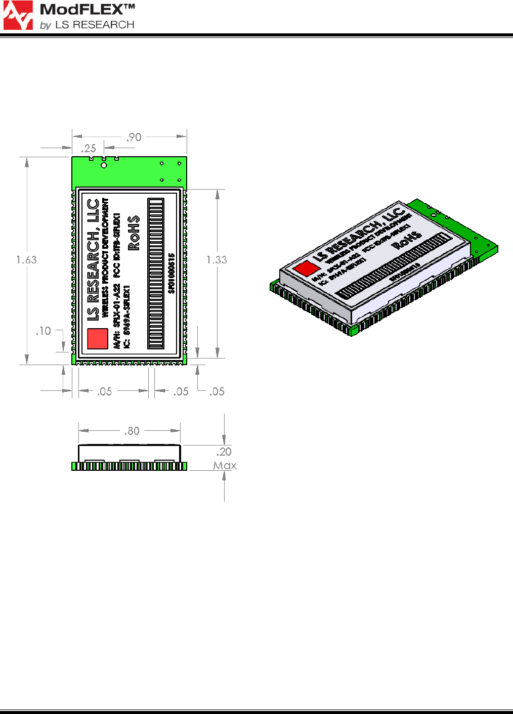
MECHANICAL DATA
General Module Dimensions
Figure 14 Basic dimensions

SiFLEX02-HP TRANSCEIVER MODULE
DATASHEET
The information in this document is subject to change without notice.
Confirm the data is current by downloading the latest revision from www.lsr.com.
330-0047-R0.7 Copyright © 2010-2011 LS Research, LLC Page 33 of 35
COMPATIBILITY
To maintain compatibility with other ModFLEX™ family transceiver modules it is important to use the
module pins in your application as they are designated in Figure 16. Since the available GPIO and
peripherals vary per micro, not all pins may be populated. For example on SiFLEX02-HP module pins
45-55 are not available (due to the number of GPIO available on the ATxMega256A3).
All attempts are made to lay out modules starting with the lowest number in the peripheral (ADC,
TMR/PWM, GPIO) series. For example if there are only two ADC’s available they will be brought out to
ADC1 and ADC2 (module pins 20 and 21).
GND 1
ModFLEX™
Generic Module Footprint
69 GND
GND 2 68 GND
GND 3 67 GND
NC 4 66 NC
NC 5 65 NC
NC 6 64 NC
NC 7 63 NC
NC 8 62 NC
JTAG - TMS 9 61 SPI - MOSI
JTAG - TDI 10 60 SPI - MISO
JTAG - TCK 11 59 SPI - SCK
JTAG - TDO 12 58 SPI - SS
JTAG/PDI/JRST 13 57 IIC - SDA
nReset 14 56 IIC - SCL
Analog REF 15 55 GPIO 16
Analog REF 16 54 GPIO 15
CMP+ 17 53 GPIO 14
CMP- 18 52 GPIO 13
CMPOUT 19 51 GPIO 12
ADC1 20 50 GPIO 11
ADC2 21 49 GPIO 10
ADC3 22 48 GPIO 9
ADC4 23 47 GPIO 8
ADC5 24 46 GPIO 7
ADC6 25 45 GPIO 6
VCC - 3V3DC 26 44 GND
27 28 29 30 31 32 33 34 35 36 37 38 39 40 41 42 43
TMR/PWM 1
TMR/PWM 2
TMR/PWM 3
TMR/PWM 4
TMR/PWM 5
TMR/PWM 6
TMR/PWM 7
TMR/PWM 8
UART - TX
UART - RX
UART - CTS
UART - RTS
GPIO 1
GPIO 2
GPIO 3
GPIO 4
GPIO 5
Figure 15 ModFLEX™ Generic Module Footprint

SiFLEX02-HP TRANSCEIVER MODULE
DATASHEET
The information in this document is subject to change without notice.
Confirm the data is current by downloading the latest revision from www.lsr.com.
330-0047-R0.7 Copyright © 2010-2011 LS Research, LLC Page 34 of 35
MODULE REVISION HISTORY
Rev 1.1
• Initial production release.

SiFLEX02-HP TRANSCEIVER MODULE
DATASHEET
The information in this document is subject to change without notice.
Confirm the data is current by downloading the latest revision from www.lsr.com.
330-0047-R0.7 Copyright © 2010-2011 LS Research, LLC Page 35 of 35
CONTACTING LS RESEARCH
Headquarters LS Research, LLC
W66 N220 Commerce Court
Cedarburg, WI 53012-2636
USA
Tel: 1(262) 375-4400
Fax: 1(262) 375-4248
Website www.lsr.com
Technical Support forum.lsr.com
Sales Contact sales@lsr.com
The information in this document is provided in connection with LS Research (hereafter referred to as “LSR”)
products. No license, express or implied, by estoppel or otherwise, to any intellectual property right is granted by
this document or in connection with the sale of LSR products. EXCEPT AS SET FORTH IN LSR’S TERMS AND
CONDITIONS OF SALE LOCATED ON LSR’S WEB SITE, LSR ASSUMES NO LIABILITY WHATSOEVER AND
DISCLAIMS ANY EXPRESS, IMPLIED OR STATUTORY WARRANTY RELATING TO ITS PRODUCTS
INCLUDING, BUT NOT LIMITED TO, THE IMPLIED WARRANTY OF MERCHANTABILITY, FITNESS FOR A
PARTICULAR PURPOSE, OR NON-INFRINGEMENT. IN NO EVENT SHALL LSR BE LIABLE FOR ANY
DIRECT, INDIRECT, CONSEQUENTIAL, PUNITIVE, SPECIAL OR INCIDENTAL DAMAGES (INCLUDING,
WITHOUT LIMITATION, DAMAGES FOR LOSS OF PROFITS, BUSINESS INTERRUPTION, OR LOSS OF
INFORMATION) ARISING OUT OF THE USE OR INABILITY TO USE THIS DOCUMENT, EVEN IF LSR HAS
BEEN ADVISED OF THE POSSIBILITY OF SUCH DAMAGES. LSR makes no representations or warranties
with respect to the accuracy or completeness of the contents of this document and reserves the right to make
changes to specifications and product descriptions at any time without notice. LSR does not make any
commitment to update the information contained herein. Unless specifically provided otherwise, LSR products
are not suitable for, and shall not be used in, automotive applications. LSR’s products are not intended,
authorized, or warranted for use as components in applications intended to support or sustain life.