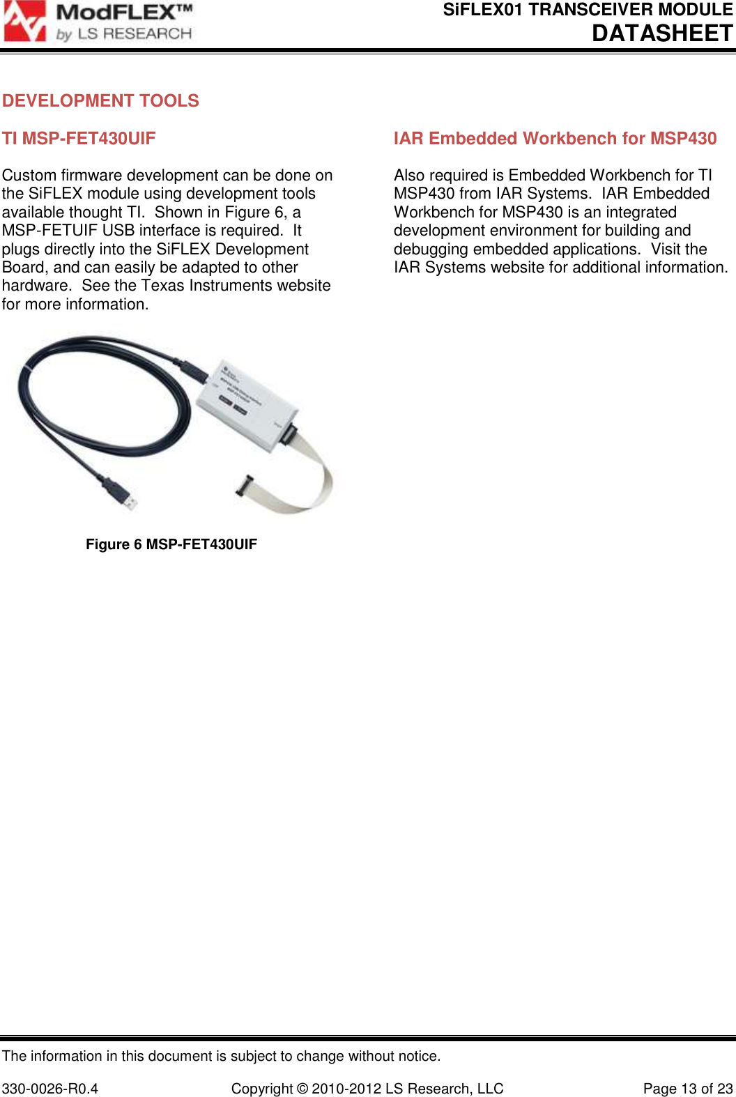
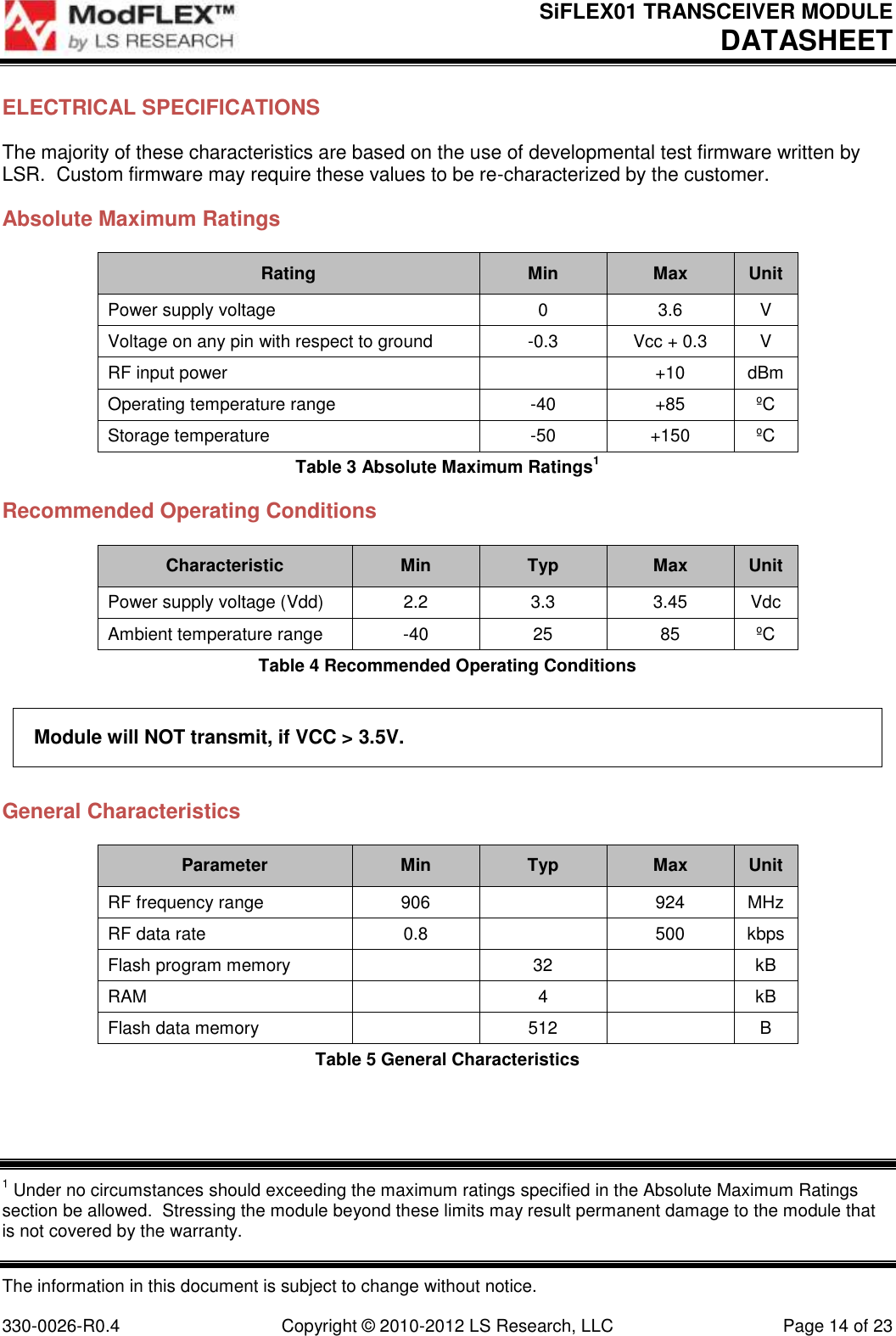
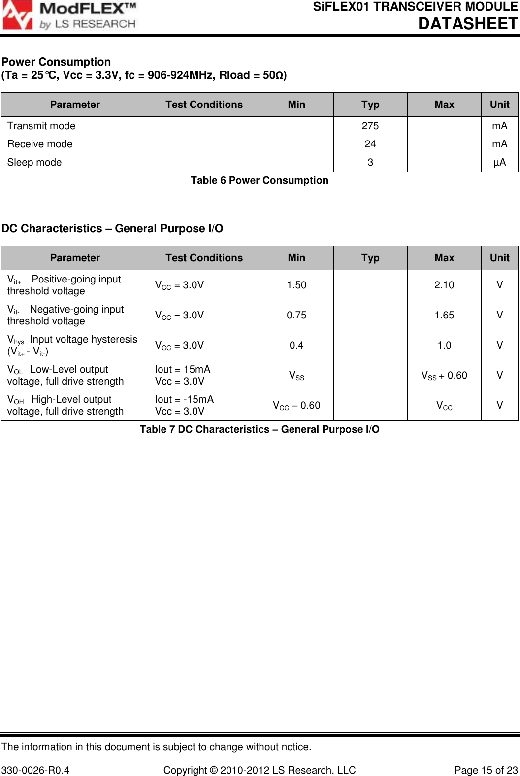
Laird Connectivity SISEN1 SiFLEX01 Module User Manual
LS Research, LLC SiFLEX01 Module
UserManual.wiki
>
Laird Connectivity
>
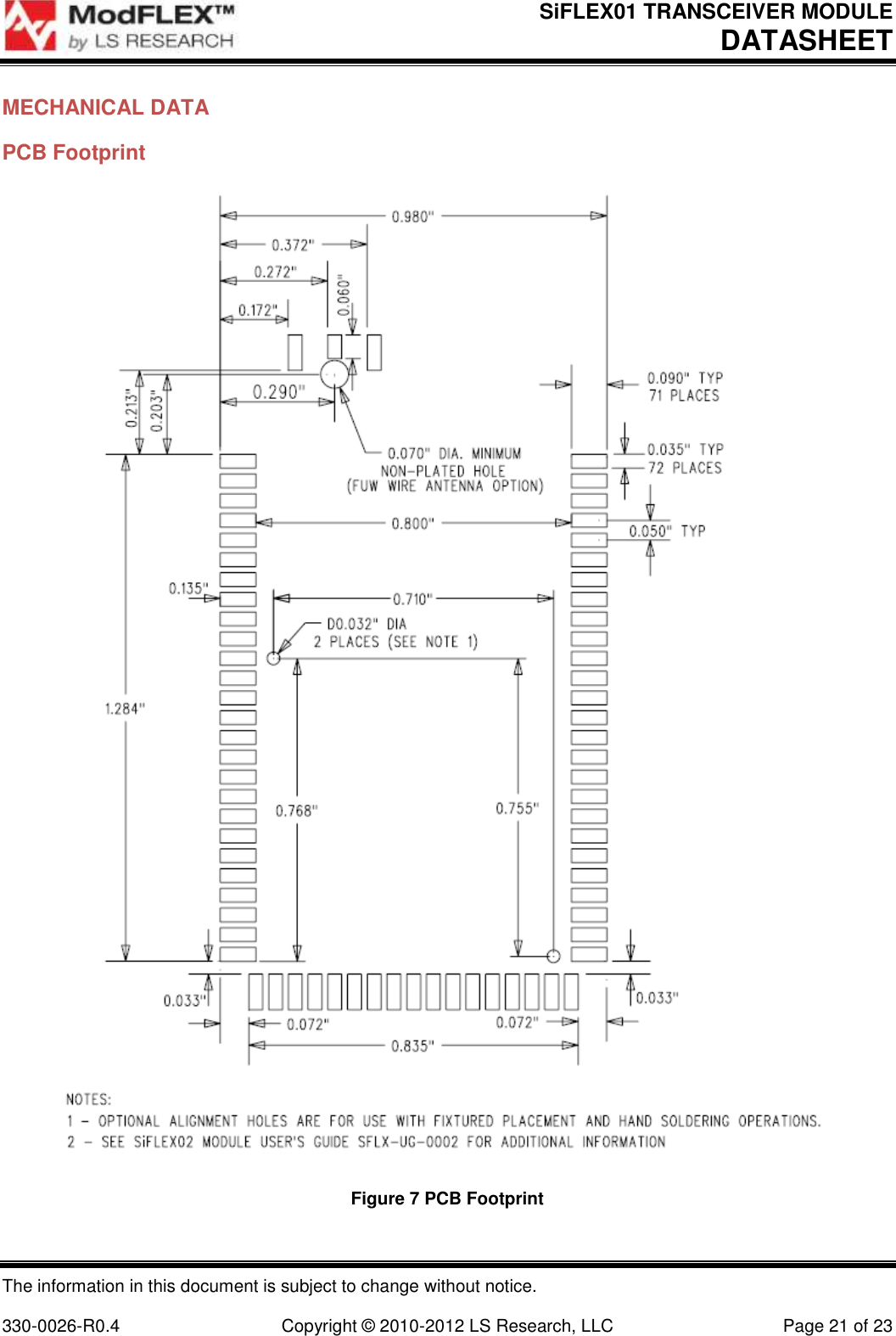
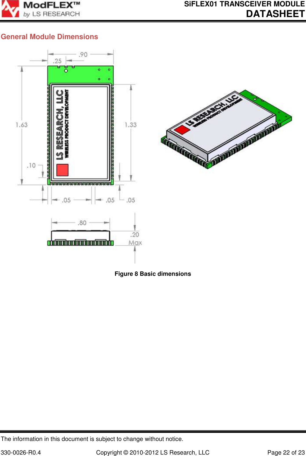
SISEN1 User Manual
User Manual
Navigation menu
Upload a User Manual
Namespaces
Wiki Guide
HTML
PDF
Info
Views
User Manual
Discussion / Help
Navigation