Laird Connectivity SISEN1 SiFLEX01 Module User Manual
LS Research, LLC SiFLEX01 Module
User Manual

SiFLEX01 TRANSCEIVER MODULE
DATASHEET
The information in this document is subject to change without notice.
330-0026-R0.4 Copyright © 2010-2012 LS Research, LLC Page 1 of 23
Integrated Transceiver Modules (900 MHz)
Development Kit Available
FEATURES
250mW output power
Long range
Up to 500 kBaud RF data rate
128 bit AES encryption available
Miniature footprint: 0.9” x 1.63”
Multiple antenna options
Certifiable for FCC and IC acceptance
MSP430 based CPU
Low power operation
RoHS compliant
Streamlined development with LSR design
services.
License options available to purchase
design or integrate design.
APPLICATIONS
Security
Lighting Control
HVAC Control
Sensor Networks
Medical
Industrial Automation
DESCRIPTION
The SiFLEX01 module is a high performance
900MHz radio based on the Texas Instruments
CC430 combined with the CC1190 front-end in
a cost effective footprint.
Need to get to market quickly? Not an expert in
frequency hopping? Need a custom antenna?
Would you like to own the design? Would you
like a custom design? Not quite sure what you
need? Do you need help with your host board?
LS Research Design Services will be happy to
develop custom hardware or software, integrate
the design, or license the design so you can
manufacture yourself. Contact us at
sales@lsr.com or call us at 262-375-4400.
SiFLEX01 TRANSCEIVER MODULE
DATASHEET
The information in this document is subject to change without notice.
330-0026-R0.4 Copyright © 2010-2012 LS Research, LLC Page 2 of 23
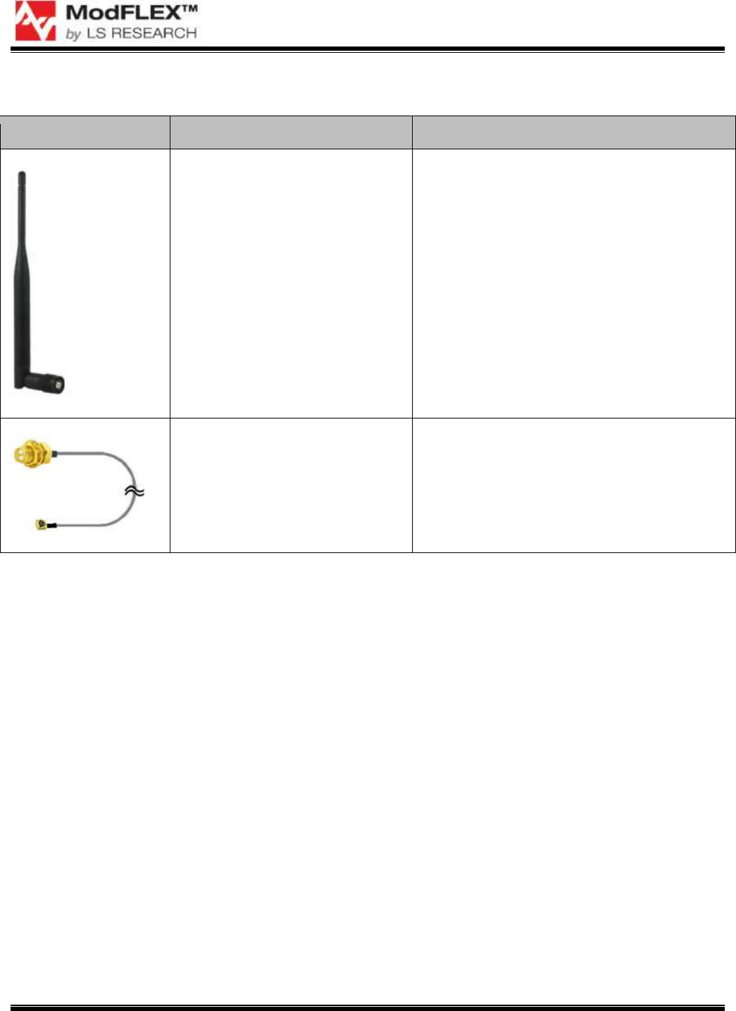
MODULE ACCESSORIES
Order Number
Description
001-0002
900 MHz Dipole Antenna with Reverse Polarity
SMA Connector
080-0001
U.FL to Reverse Polarity SMA Bulkhead Cable
105mm
SiFLEX01 TRANSCEIVER MODULE
DATASHEET
The information in this document is subject to change without notice.
330-0026-R0.4 Copyright © 2010-2012 LS Research, LLC Page 3 of 23
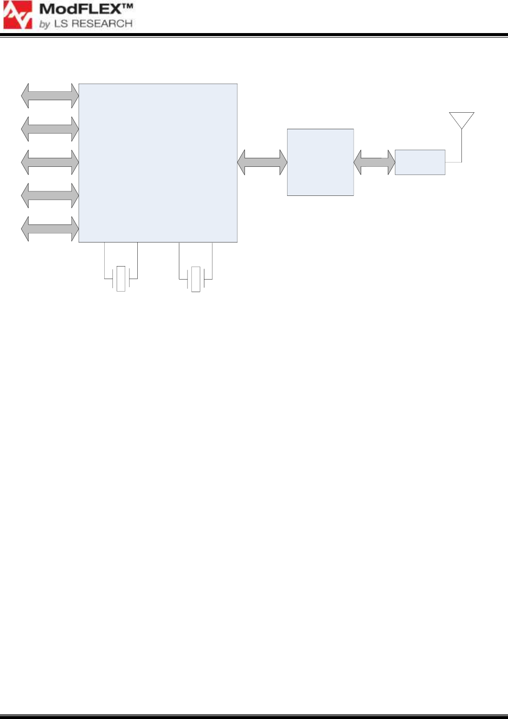
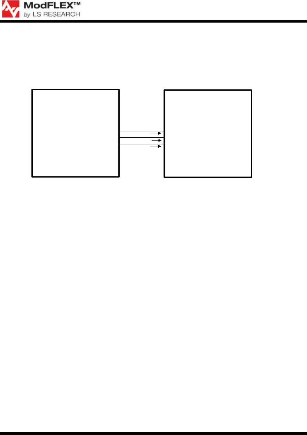
BLOCK DIAGRAM
CC430 SOC
MSP430 Microcontroller
And
900 MHz Radio Transceiver
CC1190
(PA/LNA)
Analog
JTAG
TMR/PWM
32,768 Hz 26 MHz
LPF
GPIO
Serial I/O
Figure 1 SiFLEX01 Module Block Diagram – High-Level

SiFLEX01 TRANSCEIVER MODULE
DATASHEET
The information in this document is subject to change without notice.
330-0026-R0.4 Copyright © 2010-2012 LS Research, LLC Page 4 of 23
TABLE OF CONTENTS
FEATURES .......................................................................................................................... 1
APPLICATIONS ................................................................................................................... 1
DESCRIPTION ..................................................................................................................... 1
MODULE ACCESSORIES ................................................................................................... 2
BLOCK DIAGRAM ............................................................................................................... 3
MODULE PINOUT AND PIN DESCRIPTIONS .................................................................... 5
MODULE OVERVIEW .......................................................................................................... 9
Microcontroller .......................................................................................................................................... 10
Radio .......................................................................................................................................................... 11
RF Power Amplifier ................................................................................................................................... 11
Antenna Options ....................................................................................................................................... 12
DEVELOPMENT TOOLS ................................................................................................... 13
TI MSP-FET430UIF .................................................................................................................................... 13
IAR Embedded Workbench for MSP430 ................................................................................................. 13
ELECTRICAL SPECIFICATIONS ...................................................................................... 14
Absolute Maximum Ratings ..................................................................................................................... 14
Recommended Operating Conditions .................................................................................................... 14
General Characteristics ............................................................................................................................ 14
AGENCY CERTIFICATIONS ............................................................................................. 16
AGENCY STATEMENTS ................................................................................................... 16
MECHANICAL DATA......................................................................................................... 21
PCB Footprint ............................................................................................................................................ 21
General Module Dimensions .................................................................................................................... 22
CONTACTING LS RESEARCH ......................................................................................... 23
SiFLEX01 TRANSCEIVER MODULE
DATASHEET
The information in this document is subject to change without notice.
330-0026-R0.4 Copyright © 2010-2012 LS Research, LLC Page 5 of 23
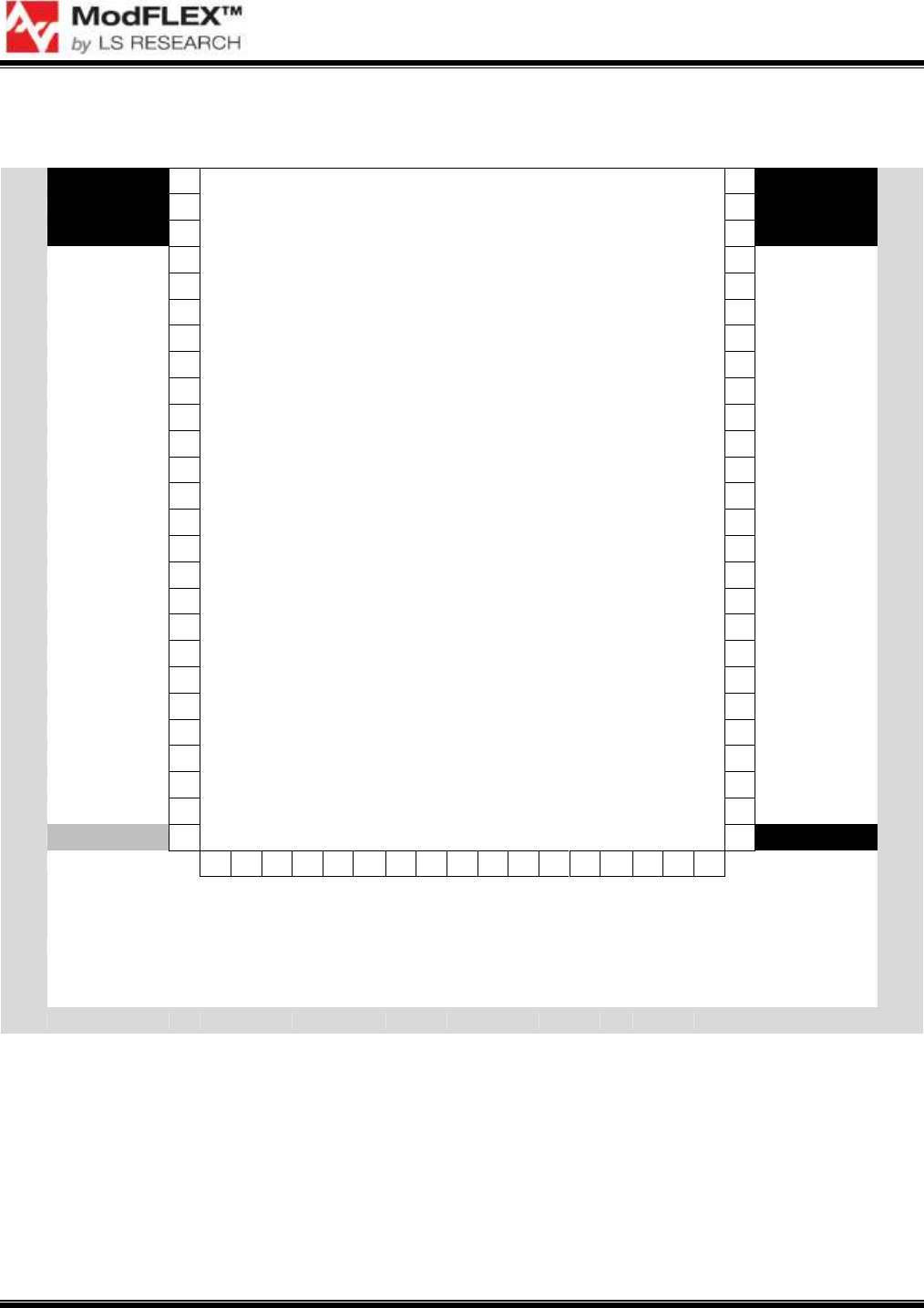
MODULE PINOUT AND PIN DESCRIPTIONS
MCU#
GND
1
Texas Instruments
CC430F6137
69
GND
MCU#
-
GND
2
68
GND
-
-
GND
3
67
GND
-
-
NC
4
66
NC
-
-
NC
5
65
NC
-
-
NC
6
64
NC
-
-
NC
7
63
NC
-
-
NC
8
62
NC
-
48
JTAG TMS
9
61
P1.3
13
47
JTAG TDI
10
60
P1.2
14
49
JTAG TCK
11
59
P1.4
12
46
JTAG TDO
12
58
P5.4
9
50
TEST
13
57
P1.3
13
51
nRESET
14
56
P1.2
14
59
P2.5
15
55
PJ.3
49
60
P2.4
16
54
PJ.2
48
58
P2.6
17
53
PJ.1
47
57
P2.7
18
52
PJ.0
46
24
P3.0
19
51
P5.3
34
64
P2.0
20
50
P5.7
6
63
P2.1
21
49
P5.6
7
62
P2.2
22
48
P4.7
26
61
P2.3
23
47
P4.6
27
60
P2.4
24
46
P4.5
28
59
P2.5
25
45
P4.4
29
-
VCC - 3V3DC
26
44
GND
-
27
28
29
30
31
32
33
34
35
36
37
38
39
40
41
42
43
P3.1
P3.2
P3.3
P3.4
P3.5
P3.6
P3.7
P3.0
P1.6
P1.5
P5.2
P5.3
P1.7
P4.0
P4.1
P4.2
P4.3
MCU#
23
22
21
20
19
18
17
24
2
3
35
34
1
33
32
31
30
MCU#
Figure 2 Module Pinout
SiFLEX01 TRANSCEIVER MODULE
DATASHEET
The information in this document is subject to change without notice.
330-0026-R0.4 Copyright © 2010-2012 LS Research, LLC Page 6 of 23
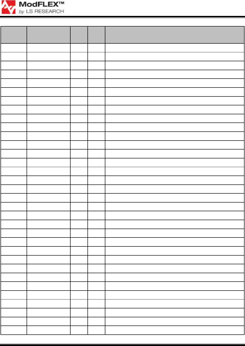
Module
Pin
Name
MCU
Pin
Type
Description
1
GND
N/A
GND
Ground
2
GND
N/A
GND
Ground
3
GND
N/A
GND
Ground
4
NC
N/A
NC
No Connect
5
NC
N/A
NC
No Connect
6
NC
N/A
NC
No Connect
7
NC
N/A
NC
No Connect
8
NC
N/A
NC
No Connect
9
JTAG TMS
48
I/O
General-purpose digital I/O (PJ.2), JTAG TMS
10
JTAG TDI
47
I/O
General-purpose digital I/O (PJ.1), JTAG TDI
11
JTAG TCK
49
I/O
General-purpose digital I/O (PJ.3), JTAG TCK
12
JTAG TDO
46
I/O
General-purpose digital I/O (PJ.0), JTAG TDO
13
TEST/SBWTCK
50
I/O
TEST / SBWTCK
14
nRESET
51
Input
/RESET / NMI / SBWTDIO
15
VREF+
59
I/O
General-purpose digital I/O (P2.5), ADC5, Analog VREF+
16
VREF-
60
I/O
General-purpose digital I/O (P2.4), ADC4, Analog VREF-
17
CMP+
58
I/O
General-purpose digital I/O (P2.6), CB6, ADC6
18
CMP-
57
I/O
General-purpose digital I/O (P2.7), CB7, ADC7
19
CMPOUT
24
I/O
General-purpose digital I/O (P3.0), CBOUT
20
ADC1
64
I/O
General-purpose digital I/O (P2.0), CB0, ADC0
21
ADC2
63
I/O
General-purpose digital I/O (P2.1), CB1, ADC1
22
ADC3
62
I/O
General-purpose digital I/O (P2.2), CB2, ADC2
23
ADC4
61
I/O
General-purpose digital I/O (P2.3), CB3, ADC3
24
ADC5
60
I/O
General-purpose digital I/O (P2.4), CB4, ADC4
25
ADC6
59
I/O
General-purpose digital I/O (P2.5), CB5, ADC5
26
VCC - 3V3DC
VCC
Supply Voltage
27
TMR/PWM1
23
I/O
General-purpose digital I/O (P3.1), TA0CCR0A
28
TMR/PWM2
22
I/O
General-purpose digital I/O (P3.2), TA0CCR1A
29
TMR/PWM3
21
I/O
General-purpose digital I/O (P3.3), TA0CCR2A
30
TMR/PWM4
20
I/O
General-purpose digital I/O (P3.4), TA0CCR3A
31
TMR/PWM5
19
I/O
General-purpose digital I/O (P3.5), TA0CCR4A
32
TMR/PWM6
18
I/O
General-purpose digital I/O (P3.6)
33
TMR/PWM7
17
I/O
General-purpose digital I/O (P3.7)

SiFLEX01 TRANSCEIVER MODULE
DATASHEET
The information in this document is subject to change without notice.
330-0026-R0.4 Copyright © 2010-2012 LS Research, LLC Page 7 of 23
Module
Pin
Name
MCU
Pin
Type
Description
34
TMR/PWM8
24
I/O
General-purpose digital I/O (P3.0), TA0CLK
35
UART TX
2
I/O
General-purpose digital I/O (P1.6), UCA0TXD
36
UART RX
3
I/O
General-purpose digital I/O (P1.5), UCA0RXD
37
UART CTS
35
I/O
General-purpose digital I/O (P5.2)
38
UART RTS
34
I/O
General-purpose digital I/O (P5.3)
39
GPIO1
1
I/O
General-purpose digital I/O (P1.7)
40
GPIO2
33
I/O
General-purpose digital I/O (P4.0)
41
GPIO3
32
I/O
General-purpose digital I/O (P4.1)
42
GPIO4
31
I/O
General-purpose digital I/O (P4.2)
43
GPIO5
30
I/O
General-purpose digital I/O (P4.3)
44
GND
GND
Ground
45
GPIO6
29
I/O
General-purpose digital I/O (P4.4)
46
GPIO7
28
I/O
General-purpose digital I/O (P4.5)
47
GPIO8
27
I/O
General-purpose digital I/O (P4.6)
48
GPIO9
26
I/O
General-purpose digital I/O (P4.7)
49
GPIO10
7
I/O
General-purpose digital I/O (P5.6)
50
GPIO11
6
I/O
General-purpose digital I/O (P5.7)
51
GPIO12
34
I/O
General-purpose digital I/O (P5.3)
52
GPIO13
46
I/O
General-purpose digital I/O (PJ.0/TDO)
53
GPIO14
47
I/O
General-purpose digital I/O (PJ.1/TDI)
54
GPIO15
48
I/O
General-purpose digital I/O (PJ.2/TMS)
55
GPIO16
49
I/O
General-purpose digital I/O (PJ.3/TCK)
56
I2C-SCL
14
I/O
General-purpose digital I/O (P1.2), UCB0SCL
57
I2C-SDA
13
I/O
General-purpose digital I/O (P1.3), UCB0SDA
58
SPI-SS
9
I/O
General-purpose digital I/O (P5.4)
59
SPI-SCK
12
I/O
General-purpose digital I/O (P1.4), UCB0CLK
60
SPI-MISO
14
I/O
General-purpose digital I/O (P1.2), UCB0SOMI
61
SPI-MOSI
13
I/O
General-purpose digital I/O (P1.3), UCB0SIMO
62
NC
N/A
NC
No Connect
63
NC
N/A
NC
No Connect
64
NC
N/A
NC
No Connect
65
NC
N/A
NC
No Connect
66
NC
N/A
NC
No Connect

SiFLEX01 TRANSCEIVER MODULE
DATASHEET
The information in this document is subject to change without notice.
330-0026-R0.4 Copyright © 2010-2012 LS Research, LLC Page 8 of 23
Module
Pin
Name
MCU
Pin
Type
Description
67
GND
N/A
GND
Ground
68
GND
N/A
GND
Ground
69
GND
N/A
GND
Ground
Table 1 SiFLEX01 Module Pin Descriptions
SiFLEX01 TRANSCEIVER MODULE
DATASHEET
The information in this document is subject to change without notice.
330-0026-R0.4 Copyright © 2010-2012 LS Research, LLC Page 9 of 23
MODULE OVERVIEW
Figure 3 shows the internal interconnects of the ICs on the SiFLEX01 module. Consult the respective
IC datasheets for details, or contact LSR sales to purchase the SiFLEX01 module schematics as part of
LSR’s ModFLEX™ design program. For a high-level block diagram of the SiFLEX01 module, see
Figure 1.
TI
CC430 TI
CC1190
HGM
LNA_EN
PA_EN
7
8
6
16
15
8
Figure 3 SiFLEX01 Module Block Diagram – Internal Interconnects
SiFLEX01 TRANSCEIVER MODULE
DATASHEET
The information in this document is subject to change without notice.
330-0026-R0.4 Copyright © 2010-2012 LS Research, LLC Page 10 of 23
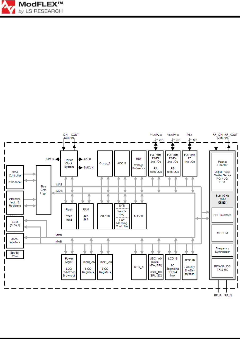
Microcontroller
The CC430 contains an MSP430 16 bit RISC core with 16 registers. The radio registers allow access
to radio functions without the bottleneck of an intermediate interface.
There are 5 modes of operation including Active Mode and 4 low power modes with progressively lower
power achieved through disabling peripherals and clocks.
RAM is organized into 2k sectors which can be powered down to save current when not in use. Data is
not retained during power-down.
A DMA controller is included to allow direct memory to memory transfers without CPU intervention.
DMA can remain active in some sleep modes for increased power savings.
A hardware AES encryption engine is included to allow 128 bit Advanced Encryption Standard (AES)
(FIPS PUB 197) to be implemented without excessive firmware burden.
Figure 4 shows a block diagram of the CC430.
Figure 4 CC430F613x Block Diagram
SiFLEX01 TRANSCEIVER MODULE
DATASHEET
The information in this document is subject to change without notice.
330-0026-R0.4 Copyright © 2010-2012 LS Research, LLC Page 11 of 23
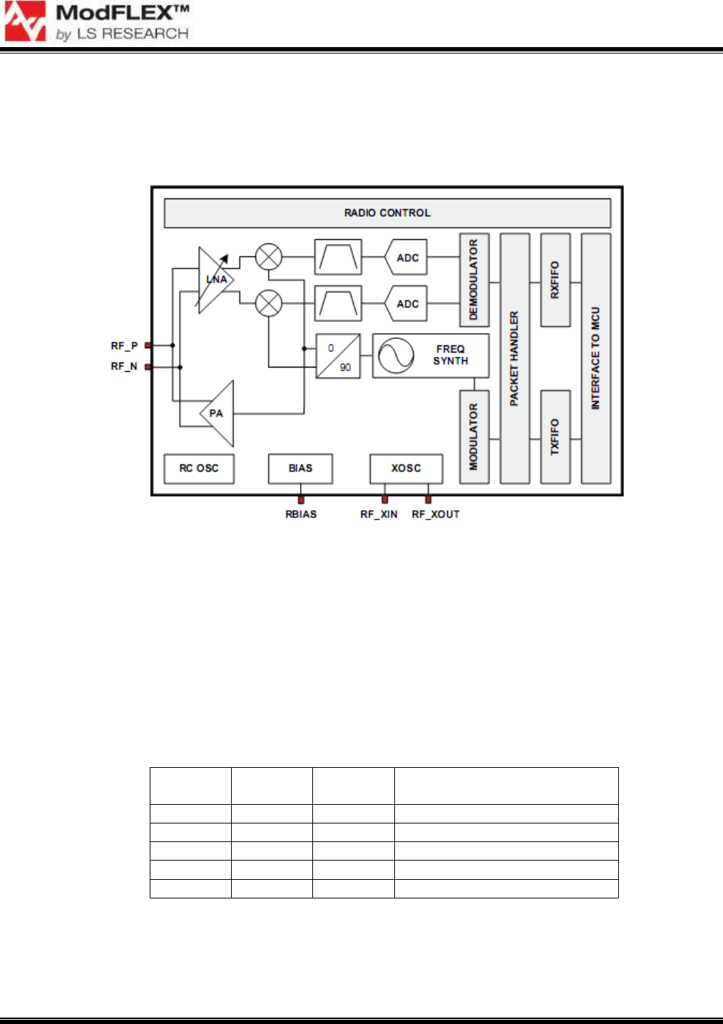
Radio
The internal radio is based on the TI CC1101. It is a low-IF type with all digital AGC and filtering.
Memory mapped registers are used for data access and controlling radio characteristics.
Figure 5 CC430 Sub 1 GHz Radio Block Diagram
RF Power Amplifier
The SiFLEX01 module contains a TI CC1190 front-end chip. It is capable of 250mW output power.
When transmitting the PA_EN signal will be high and LNA_EN will be low, which is controlled by the
firmware using GPIO pins P1.0 and P1.1. When receiving PA_EN is low and LNA_EN is high. LNA
gang is be adjusted to a high or low setting with the HGM signal controlled by P5.5.
PA_EN
P1.0
LNA_EN
P1.1
HGM
P5.5
Operation
0
0
X
Shutdown
0
1
0
RX low gain
0
1
1
RX high gain
1
0
0
TX low gain
1
0
1
TX high gain
Table 2 Front-end control functions

SiFLEX01 TRANSCEIVER MODULE
DATASHEET
The information in this document is subject to change without notice.
330-0026-R0.4 Copyright © 2010-2012 LS Research, LLC Page 12 of 23
Antenna Options
The SiFLEX01 module includes multiple antenna options. The module regulatory certification can be
completed with the following options:
Certified Antenna Options
LSR 001-0002 900 MHz Dipole Antenna with Reverse Polarity SMA Connector and LSR 080-
0001 U.FL to Reverse Polarity SMA Bulkhead Cable 105mm.
Antenna Factor ANT-916-CW-HWR-RPS 900 MHz Dipole Antenna with Reverse Polarity SMA
Connector and PanguTech JQ-0036-L4 MMCX to Reverse Polarity SMA Cable.
Non-certified Antenna Options
Integrated 3.2-inch wire monopole soldered to the board.
Off-board antenna using the castellated edge connection to a 50Ω trace on the host board
An adequate ground plane is necessary to provide good efficiency. The ground plane of the host board
on which the module is mounted increases the effective antenna ground plane size and improves the
antenna performance.
The environment the module is placed in will dictate the range performance The non-ideal
characteristics of the environment will result in the transmitted signal being reflected, diffracted, and
scattered. All of these factors randomly combine to create extremely complex scenarios that will affect
the link range in various ways.
It is also best to keep some clearance between the antenna and nearby objects. This includes how the
module is mounted in the product enclosure. Unless the items on the following list of recommendations
are met, the radiation pattern can be heavily distorted.
Whichever antenna is used, it is best to keep a few things in mind when determining its location.
Never place ground plane or copper trace routing underneath the antenna.
LSR recommends keeping metal objects as far away from the antenna as possible. At a very
minimum keep the antenna at least 5 cm from any metallic objects, components, or wiring. The
farther the antenna is placed from these interferers, the less the radiation pattern and gain will
be perturbed.
Do not embed the antenna in a metallic or metalized plastic enclosure.
If located within a plastic enclosure, keep the enclosure at least 1 cm from the antenna.
SiFLEX01 TRANSCEIVER MODULE
DATASHEET
The information in this document is subject to change without notice.
330-0026-R0.4 Copyright © 2010-2012 LS Research, LLC Page 13 of 23
DEVELOPMENT TOOLS
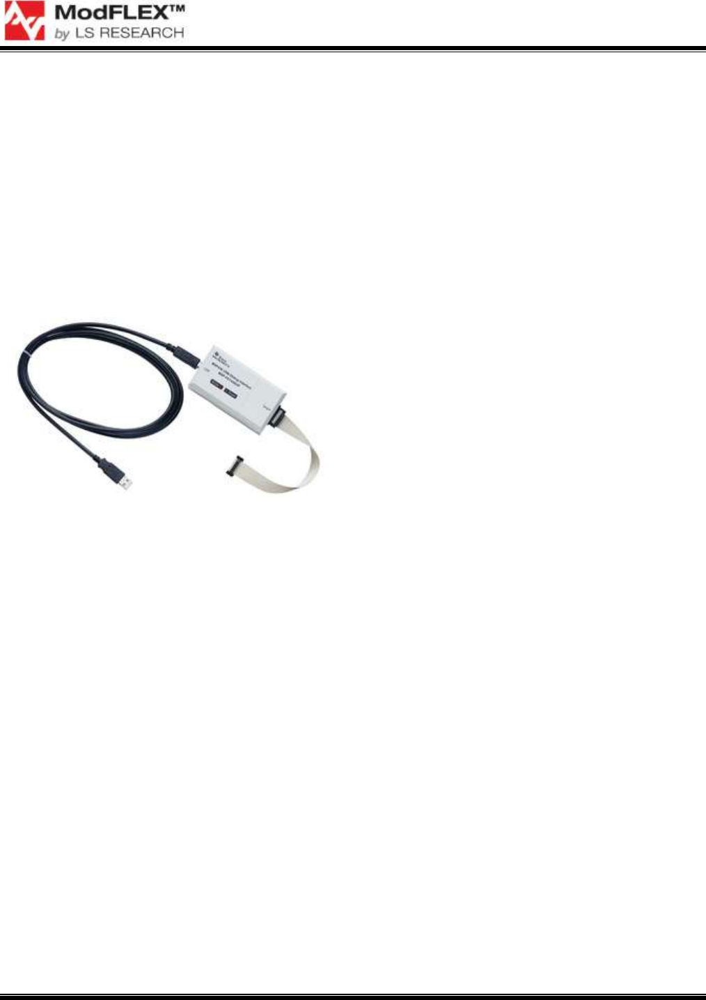
TI MSP-FET430UIF
Custom firmware development can be done on
the SiFLEX module using development tools
available thought TI. Shown in Figure 6, a
MSP-FETUIF USB interface is required. It
plugs directly into the SiFLEX Development
Board, and can easily be adapted to other
hardware. See the Texas Instruments website
for more information.
Figure 6 MSP-FET430UIF
IAR Embedded Workbench for MSP430
Also required is Embedded Workbench for TI
MSP430 from IAR Systems. IAR Embedded
Workbench for MSP430 is an integrated
development environment for building and
debugging embedded applications. Visit the
IAR Systems website for additional information.
SiFLEX01 TRANSCEIVER MODULE
DATASHEET
The information in this document is subject to change without notice.
330-0026-R0.4 Copyright © 2010-2012 LS Research, LLC Page 14 of 23
ELECTRICAL SPECIFICATIONS
The majority of these characteristics are based on the use of developmental test firmware written by
LSR. Custom firmware may require these values to be re-characterized by the customer.
Absolute Maximum Ratings
Rating
Min
Max
Unit
Power supply voltage
0
3.6
V
Voltage on any pin with respect to ground
-0.3
Vcc + 0.3
V
RF input power
+10
dBm
Operating temperature range
-40
+85
ºC
Storage temperature
-50
+150
ºC
Table 3 Absolute Maximum Ratings
1
Recommended Operating Conditions
Characteristic
Min
Typ
Max
Unit
Power supply voltage (Vdd)
2.2
3.3
3.45
Vdc
Ambient temperature range
-40
25
85
ºC
Table 4 Recommended Operating Conditions
Module will NOT transmit, if VCC > 3.5V.
General Characteristics
Parameter
Min
Typ
Max
Unit
RF frequency range
906
924
MHz
RF data rate
0.8
500
kbps
Flash program memory
32
kB
RAM
4
kB
Flash data memory
512
B
Table 5 General Characteristics
1
Under no circumstances should exceeding the maximum ratings specified in the Absolute Maximum Ratings
section be allowed. Stressing the module beyond these limits may result permanent damage to the module that
is not covered by the warranty.
SiFLEX01 TRANSCEIVER MODULE
DATASHEET
The information in this document is subject to change without notice.
330-0026-R0.4 Copyright © 2010-2012 LS Research, LLC Page 15 of 23
Power Consumption
(Ta = 25°C, Vcc = 3.3V, fc = 906-924MHz, Rload = 50Ω)
Parameter
Test Conditions
Min
Typ
Max
Unit
Transmit mode
275
mA
Receive mode
24
mA
Sleep mode
3
µA
Table 6 Power Consumption
DC Characteristics – General Purpose I/O
Parameter
Test Conditions
Min
Typ
Max
Unit
Vit+ Positive-going input
threshold voltage
VCC = 3.0V
1.50
2.10
V
Vit- Negative-going input
threshold voltage
VCC = 3.0V
0.75
1.65
V
Vhys Input voltage hysteresis
(Vit+ - Vit-)
VCC = 3.0V
0.4
1.0
V
VOL Low-Level output
voltage, full drive strength
Iout = 15mA
Vcc = 3.0V
VSS
VSS + 0.60
V
VOH High-Level output
voltage, full drive strength
Iout = -15mA
Vcc = 3.0V
VCC – 0.60
VCC
V
Table 7 DC Characteristics – General Purpose I/O

SiFLEX01 TRANSCEIVER MODULE
DATASHEET
The information in this document is subject to change without notice.
330-0026-R0.4 Copyright © 2010-2012 LS Research, LLC Page 16 of 23
AGENCY CERTIFICATIONS
FCC ID: TFB-SISEN1, 15.247
IC ID: 5969A-SISEN1, RSS 210
AGENCY STATEMENTS
Federal Communication Commission Interference Statement
This equipment has been tested and found to comply with the limits for a Class B digital device,
pursuant to Part 15 of the FCC Rules. These limits are designed to provide reasonable protection
against harmful interference in a residential installation. This equipment generates uses and can radiate
radio frequency energy and, if not installed and used in accordance with the instructions, may cause
harmful interference to radio communications. However, there is no guarantee that interference will not
occur in a particular installation. If this equipment does cause harmful interference to radio or television
reception, which can be determined by turning the equipment off and on, the user is encouraged to try
to correct the interference by one of the following measures:
Reorient or relocate the receiving antenna.
Increase the separation between the equipment and receiver.
Connect the equipment into an outlet on a circuit different from that to which the receiver is
connected.
Consult the dealer or an experienced radio/TV technician for help.
This device complies with Part 15 of the FCC Rules. Operation is subject to the following two
conditions: (1) This device may not cause harmful interference, and (2) this device must accept any
interference received, including interference that may cause undesired operation.
FCC CAUTION: Any changes or modifications not expressly approved by the party
responsible for compliance could void the user's authority to operate this equipment.

SiFLEX01 TRANSCEIVER MODULE
DATASHEET
The information in this document is subject to change without notice.
330-0026-R0.4 Copyright © 2010-2012 LS Research, LLC Page 17 of 23
Industry Canada Statements
Operation is subject to the following two conditions: (1) this device may not cause interference, and (2)
this device must accept any interference, including interference that may cause undesired operation of
the device.
To reduce potential radio interference to other users, the antenna type and its gain should be so
chosen that the equivalent isotropically radiated power (e.i.r.p.) is not more than that permitted for
successful communication.
This device has been designed to operate with the antennas listed below, and having a maximum gain
of 2 dBi (LS Research dipole) and 2 dBi (Antenna Factor dipole). Antennas not included in this list or
having a gain greater than 2 dBi and 2 dBi are strictly prohibited for use with this device. The required
antenna impedance is 50 ohms.
List of all Antennas Acceptable for use with the Transmitter
1) LS Research 001-0002 900 MHz Dipole Antenna with Reverse Polarity SMA Connector and
LS Research 080-0001 U.FL to Reverse Polarity SMA Cable.
2) Antenna Factor ANT-916-CW-HWR-RPS 900 MHz Dipole Antenna with Reverse Polarity
SMA Connector and PanguTech JQ-0036-L4 MMCX to Reverse Polarity SMA Cable.
Son fonctionnement est soumis aux deux conditions suivantes: (1) cet appareil ne peut pas provoquer
d'interférences et (2) cet appareil doit accepter toute interférence, y compris les interférences qui
peuvent causer un mauvais fonctionnement du dispositif.
Pour réduire le risque d'interférence aux autres utilisateurs, le type d'antenne et son gain doivent être
choisies de façon que la puissance isotrope rayonnée équivalente (e.i.r.p) ne dépasse pas celle admise
pour une communication réussie.
Cet appareil a été conçu pour fonctionner avec les antennes énumérées ci-dessous, et d'avoir un
gain maximum de 2 dBi (LS Research dipôle) et 2 dBi (Antenna Factor dipôle). Antennes pas inclus
dans cette liste ou d'avoir un gain plus grand que 2 et 2 dBi dBi sont strictement interdites pour
l'utilisation avec cet appareil. L'impédance d'antenne requise est de 50 ohms.
Liste de toutes les antennes acceptables pour une utilisation avec l'émetteur
1) LS Research 900 001-0002 antenne dipôle MHz avec connecteur SMA inversé la polarité et
de la LS Research LS 080-0001 U. FL à Reverse SMA à polarité du câble.
2) Antenna Factor ANT-916-CW-HWR-RPS 900 MHz Antenne dipôleavec connecteur SMA
inversé la polarité et la PanguTech JQ-0036-L4 MMCX pour câble SMA inversé la polarité.

SiFLEX01 TRANSCEIVER MODULE
DATASHEET
The information in this document is subject to change without notice.
330-0026-R0.4 Copyright © 2010-2012 LS Research, LLC Page 18 of 23
OEM Responsibilities to comply with FCC and Industry Canada Regulations
The SiFLEX01 Module has been certified for integration into products only by OEM integrators under
the following conditions:
This device is granted for use in Mobile only configurations in which the antennas used for this
transmitter must be installed to provide a separation distance of at least 20cm from all person and not
be co-located with any other transmitters except in accordance with FCC and Industry Canada multi-
transmitter product procedures.
As long as the two conditions above are met, further transmitter testing will not be required. However,
the OEM integrator is still responsible for testing their end-product for any additional compliance
requirements required with this module installed (for example, digital device emissions, PC peripheral
requirements, etc.).
IMPORTANT NOTE: In the event that these conditions cannot be met (for certain
configurations or co-location with another transmitter), then the FCC and Industry
Canada authorizations are no longer considered valid and the FCC ID and IC Certification
Number cannot be used on the final product. In these circumstances, the OEM integrator
will be responsible for re-evaluating the end product (including the transmitter) and
obtaining a separate FCC and Industry Canada authorization.
Le module SiFLEX01 a été certifiée pour l'intégration dans les produits que par les intégrateurs OEM
dans les conditions suivantes:
Ce dispositif est accordé pour une utilisation dans des configurations mobiles seule dans laquelle les
antennes utilisées pour cet émetteur doit être installé pour fournir une distance de séparation d'au
moins 20cm de toute personne et ne pas être co-localisés avec les autres émetteurs, sauf en
conformité avec FCC et Industrie Canada, multi-émetteur procédures produit.
Tant que les deux conditions précitées sont réunies, les tests de transmetteurs supplémentaires ne
seront pas tenus. Toutefois, l'intégrateur OEM est toujours responsable de tester leur produit final pour
toutes les exigences de conformité supplémentaires requis avec ce module installé (par exemple, les
émissions appareil numérique, les exigences de périphériques PC, etc.)
NOTE IMPORTANTE: Dans le cas où ces conditions ne peuvent être satisfaites (pour
certaines configurations ou de co-implantation avec un autre émetteur), puis la FCC et
Industrie autorisations Canada ne sont plus considérés comme valides et l'ID de la FCC
et IC numéro de certification ne peut pas être utilisé sur la produit final. Dans ces
circonstances, l'intégrateur OEM sera chargé de réévaluer le produit final (y compris
l'émetteur) et l'obtention d'un distincte de la FCC et Industrie Canada l'autorisation.

SiFLEX01 TRANSCEIVER MODULE
DATASHEET
The information in this document is subject to change without notice.
330-0026-R0.4 Copyright © 2010-2012 LS Research, LLC Page 19 of 23
End Product Labelling
The SiFLEX01 Module is labeled with its own FCC ID and IC Certification Number. If the FCC ID and
IC Certification Number are not visible when the module is installed inside another device, then the
outside of the device into which the module is installed must also display a label referring to the
enclosed module. In that case, the final end product must be labeled in a visible area with the
following:
“Contains Transmitter Module FCC ID: TFB-SISEN1”
“Contains Transmitter Module IC: 5969A-SISEN1”
or
“Contains FCC ID: TFB-SISEN1”
“Contains IC: 5969A-SISEN1”
The OEM of the SiFLEX01 Module must only use the approved antenna(s) listed above, which have
been certified with this module.
The OEM integrator has to be aware not to provide information to the end user regarding how to install
or remove this RF module or change RF related parameters in the user manual of the end product.
The user manual for the end product must include the following information in a prominent
location:
This device is granted for use in Mobile only configurations in which the antennas used for this
transmitter must be installed to provide a separation distance of at least 20cm from all person
and not be co-located with any other transmitters except in accordance with FCC and Industry
Canada multi-transmitter product procedures.

SiFLEX01 TRANSCEIVER MODULE
DATASHEET
The information in this document is subject to change without notice.
330-0026-R0.4 Copyright © 2010-2012 LS Research, LLC Page 20 of 23
Le SiFLEX01 Module est étiqueté avec sa propre ID de la FCC et IC numéro de certification. Si l'ID de
la FCC et IC numéro de certification ne sont pas visibles lorsque le module est installé à l'intérieur d'un
autre appareil, puis l'extérieur de l'appareil dans lequel le module est installé doit également afficher
une étiquette mentionnant le module ci-joint. Dans ce cas, le produit final doivent être étiquetés dans
un endroit visible de ce qui suit:
Module émetteur Contient FCC ID: TFB-SISEN1
Module émetteur Contient IC: 5969A-SISEN1
ou
Contient FCC ID: TFB-SISEN1
Contient IC: 5969A-SISEN1
Le constructeur d'équipements de l’ SiFLEX01 module ne doit utiliser l'antenne approuvée (s) ci-
dessus, qui ont été certifiés avec ce module.
L'intégrateur OEM doit être conscient de ne pas fournir des informations à l'utilisateur final quant à la
façon d'installer ou de supprimer ce module RF ou RF changer les paramètres liés au mode d'emploi
du produit final.
Le manuel d'utilisation pour le produit final doit comporter les informations suivantes dans un
endroit bien en vue:
Ce dispositif est accordé pour une utilisation dans des configurations mobiles
seule dans laquelle les antennes utilisées pour cet émetteur doit être installé
pour fournir une distance de séparation d'au moins 20cm de toute personne et
ne pas être co-localisés avec les autres émetteurs, sauf en conformité avec FCC
et Industrie Canada, multi-émetteur procedures produit.
SiFLEX01 TRANSCEIVER MODULE
DATASHEET
The information in this document is subject to change without notice.
330-0026-R0.4 Copyright © 2010-2012 LS Research, LLC Page 21 of 23
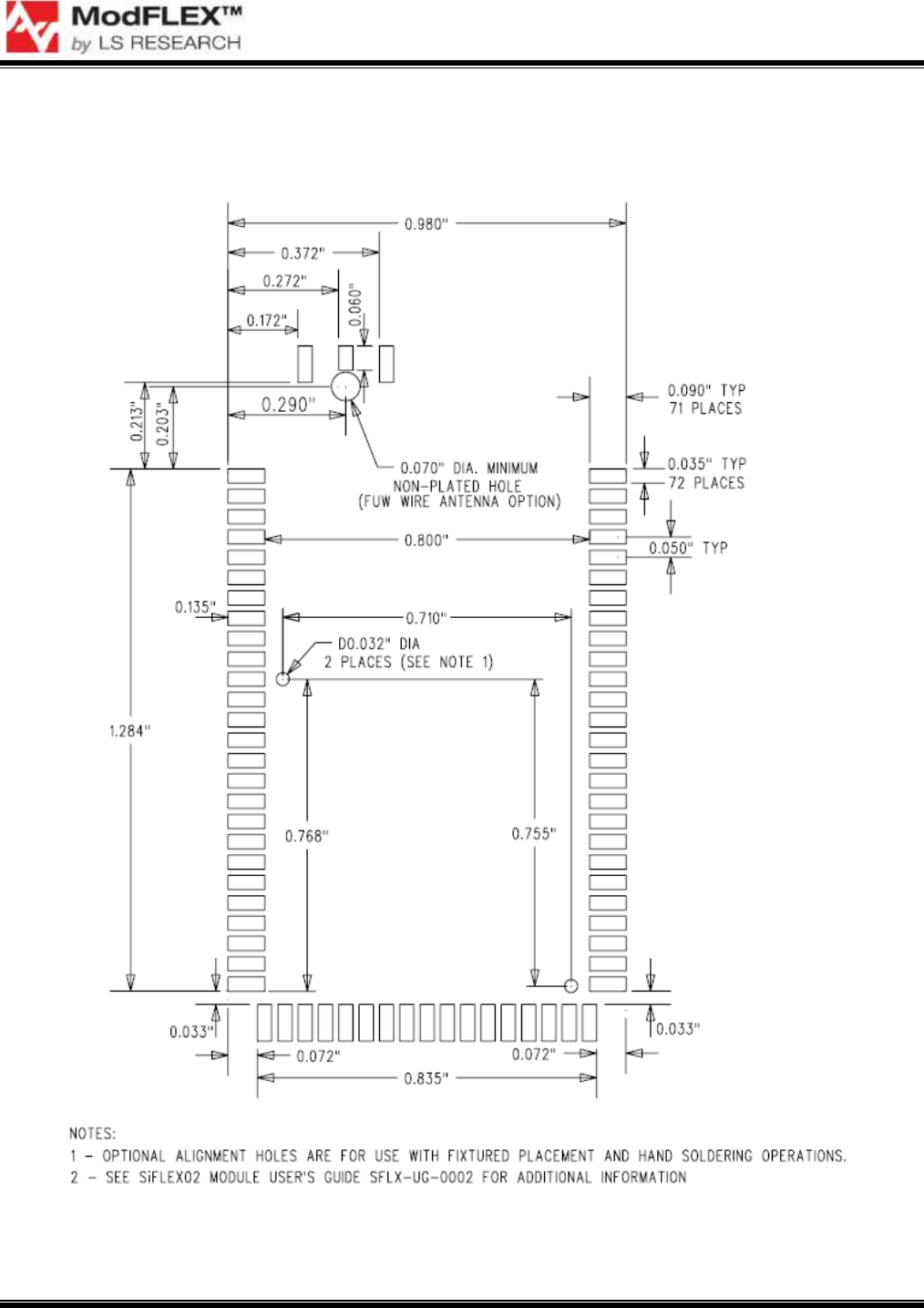
MECHANICAL DATA
PCB Footprint
Figure 7 PCB Footprint
SiFLEX01 TRANSCEIVER MODULE
DATASHEET
The information in this document is subject to change without notice.
330-0026-R0.4 Copyright © 2010-2012 LS Research, LLC Page 22 of 23
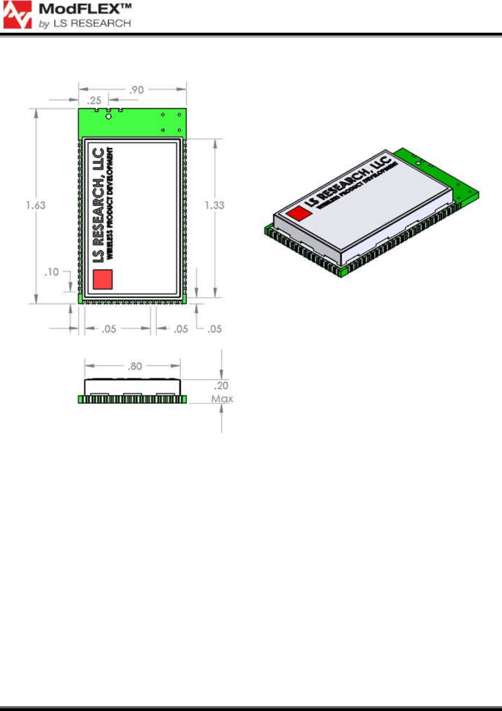
General Module Dimensions
Figure 8 Basic dimensions

SiFLEX01 TRANSCEIVER MODULE
DATASHEET
The information in this document is subject to change without notice.
330-0026-R0.4 Copyright © 2010-2012 LS Research, LLC Page 23 of 23
CONTACTING LS RESEARCH
Headquarters LS Research, LLC
W66 N220 Commerce Court
Cedarburg, WI 53012-2636
USA
Tel: 1(262) 375-4400
Fax: 1(262) 375-4248
Website www.lsr.com
Technical Support forum.lsr.com
Sales Contact sales@lsr.com
The information in this document is provided in connection with LS Research (hereafter referred to as “LSR”)
products. No license, express or implied, by estoppel or otherwise, to any intellectual property right is granted by
this document or in connection with the sale of LSR products. EXCEPT AS SET FORTH IN LSR’S TERMS AND
CONDITIONS OF SALE LOCATED ON LSR’S WEB SITE, LSR ASSUMES NO LIABILITY WHATSOEVER AND
DISCLAIMS ANY EXPRESS, IMPLIED OR STATUTORY WARRANTY RELATING TO ITS PRODUCTS
INCLUDING, BUT NOT LIMITED TO, THE IMPLIED WARRANTY OF MERCHANTABILITY, FITNESS FOR A
PARTICULAR PURPOSE, OR NON-INFRINGEMENT. IN NO EVENT SHALL LSR BE LIABLE FOR ANY
DIRECT, INDIRECT, CONSEQUENTIAL, PUNITIVE, SPECIAL OR INCIDENTAL DAMAGES (INCLUDING,
WITHOUT LIMITATION, DAMAGES FOR LOSS OF PROFITS, BUSINESS INTERRUPTION, OR LOSS OF
INFORMATION) ARISING OUT OF THE USE OR INABILITY TO USE THIS DOCUMENT, EVEN IF LSR HAS
BEEN ADVISED OF THE POSSIBILITY OF SUCH DAMAGES. LSR makes no representations or warranties
with respect to the accuracy or completeness of the contents of this document and reserves the right to make
changes to specifications and product descriptions at any time without notice. LSR does not make any
commitment to update the information contained herein. Unless specifically provided otherwise, LSR products
are not suitable for, and shall not be used in, automotive applications. LSR’s products are not intended,
authorized, or warranted for use as components in applications intended to support or sustain life.