Laird Connectivity TIWISL01 TiWi-SL User Manual
LS Research, LLC TiWi-SL
UserManual.wiki
>
Laird Connectivity
>
TIWISL01 User Manual
User Manual
Navigation menu
Upload a User Manual
Namespaces
Wiki Guide
HTML
PDF
Info
Views
User Manual
Discussion / Help
Navigation
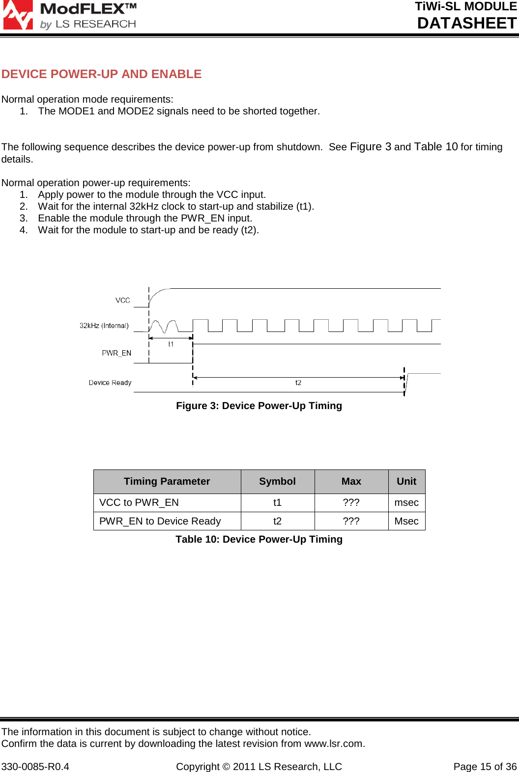
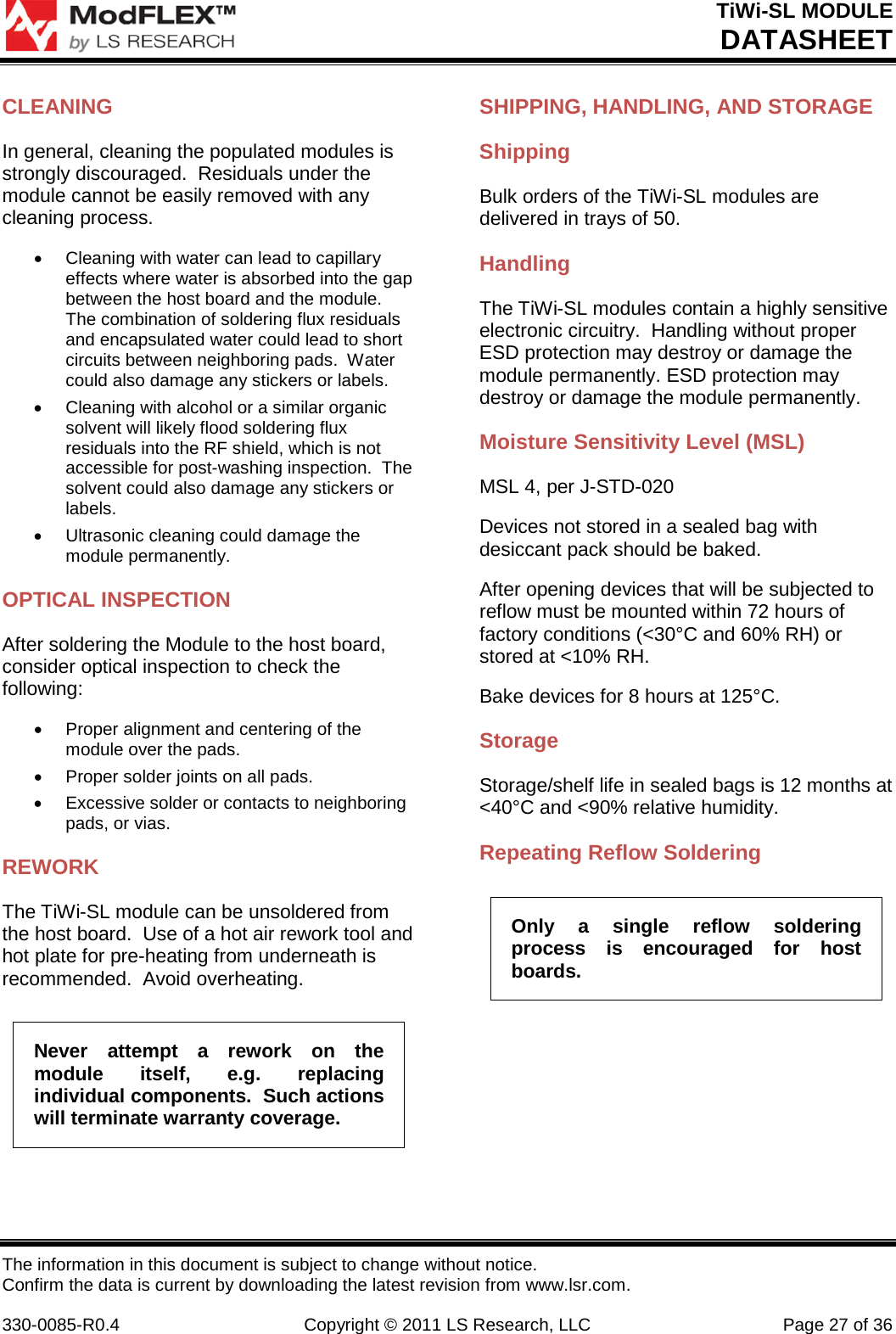
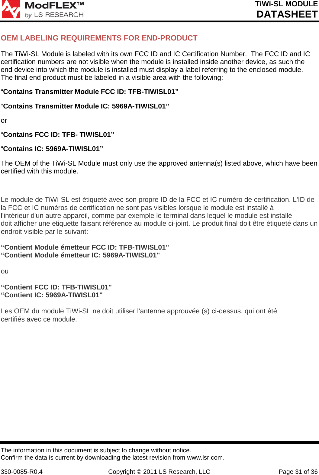
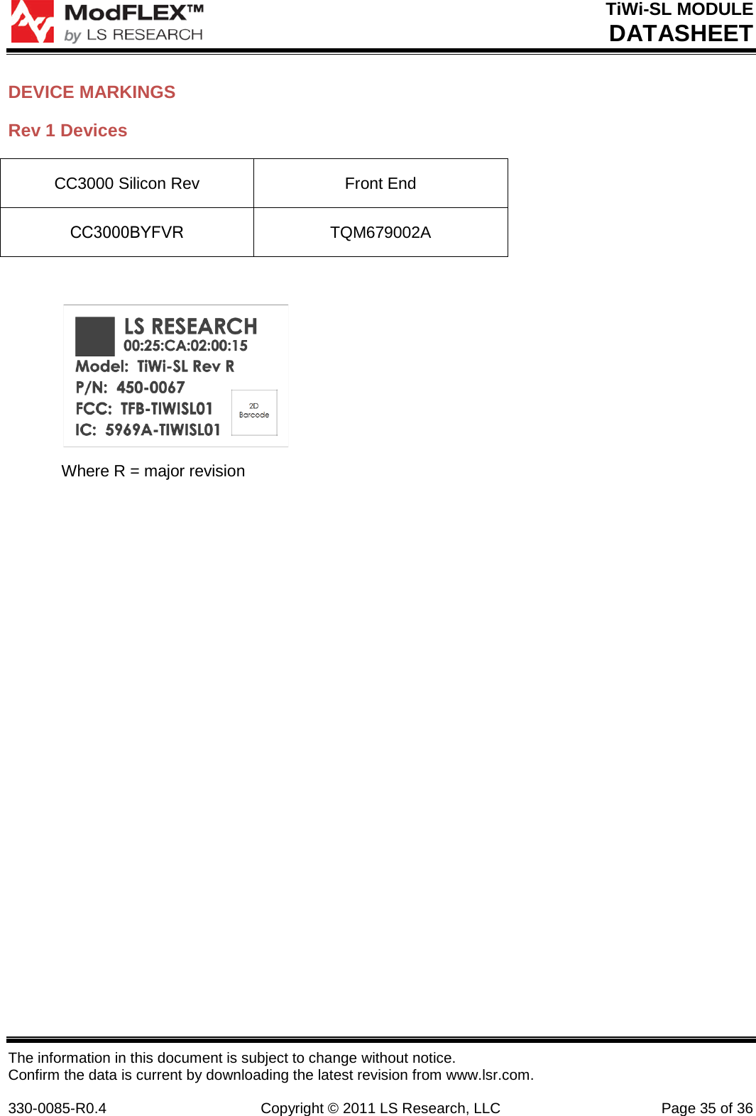
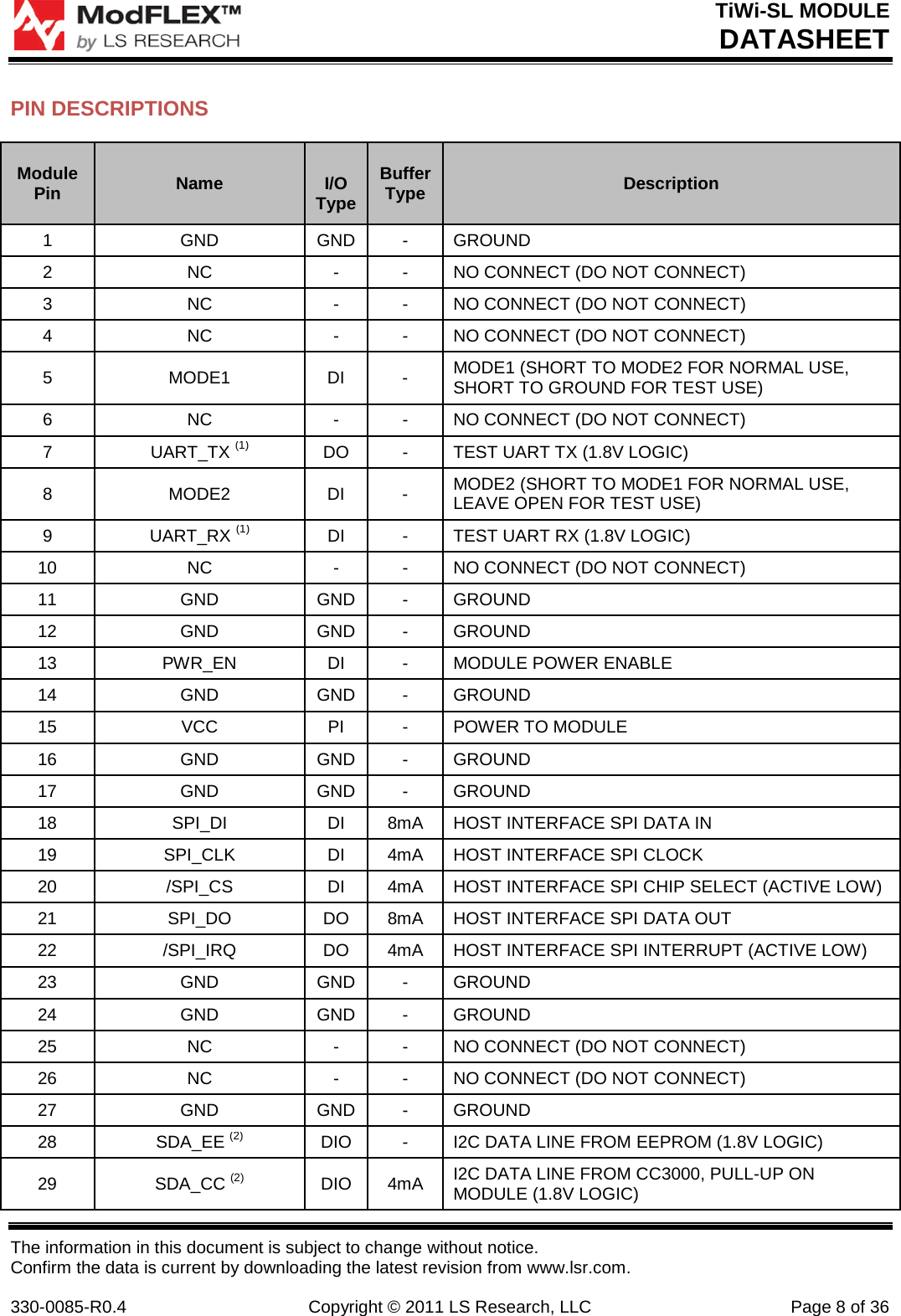
![TiWi-SL MODULE DATASHEET The information in this document is subject to change without notice. Confirm the data is current by downloading the latest revision from www.lsr.com. 330-0085-R0.4 Copyright © 2011 LS Research, LLC Page 4 of 36 FUNCTIONAL BLOCK FEATURES WLAN Features • WLAN MAC Baseband Processor and RF transceiver which is IEEE802.11b/g compliant • Accepts 26MHz reference clock Input • IEEE Std 802.11d,i PICS compliant • Supports serial debug interface • Supports Serial Peripheral Interface (SPI) Host Interface • Medium-Access Controller (MAC) o Embedded ARM™ Central Processing Unit (CPU) o Hardware-Based Encryption/Decryption Using 64-, 128-Bit WEP, TKIP or AES Keys, o Supports requirements for Wireless Fidelity (Wi-Fi) Protected Access (WPA and WPA2.0) and IEEE o Std 802.11i [Includes Hardware-Accelerated Advanced-Encryption Standard (AES)] • Baseband Processor • 2.4GHz Radio o Digital Radio Processor (DRP) implementation o Internal LNA o Supports : IEEE Std 802.11b, 802.11g, 802.11b/g Network Stack Supported Protocols • Transport layer: o TCP o UDP • Network layer: o IPv4 o Ping o DHCP o DNS Client • Link layer: o ARP Wireless Security System Features • Supported modes: o Open (no security) o WEP o WPA-personal o WPA2-personal • Supported encryption types: o WEP o TKIP o AES o Open](https://usermanual.wiki/Laird-Connectivity/TIWISL01/User-Guide-1600739-Page-4.png)
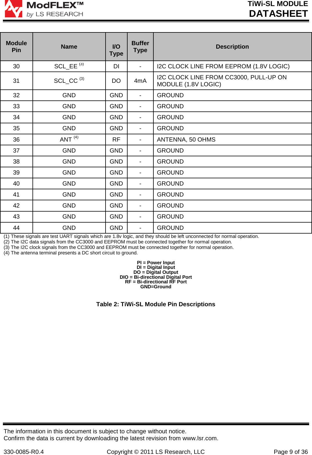
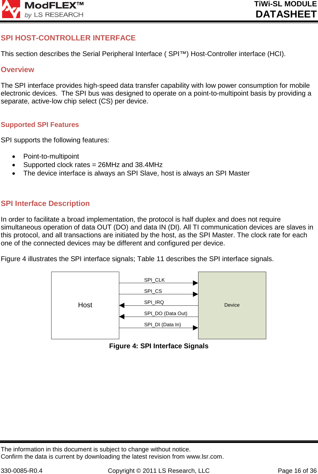
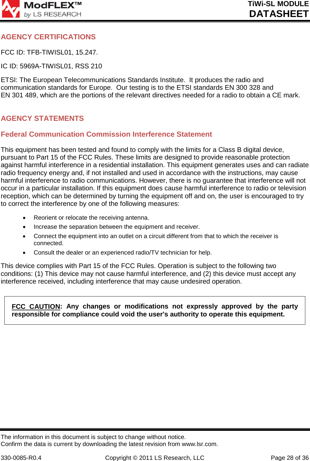
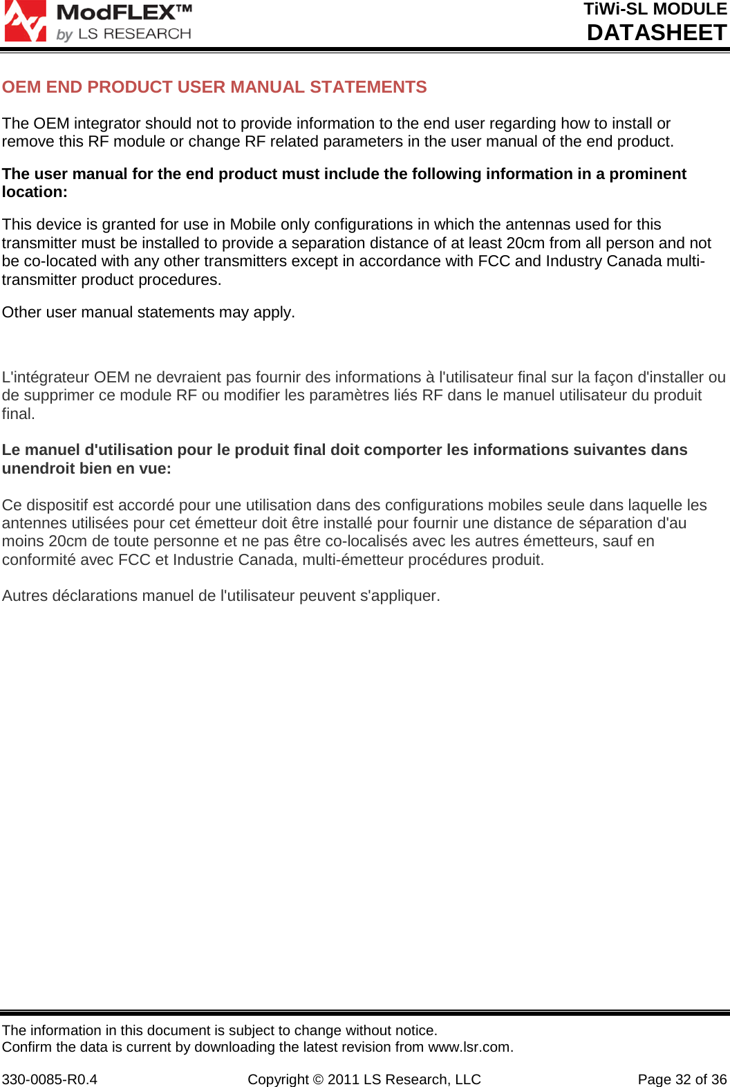
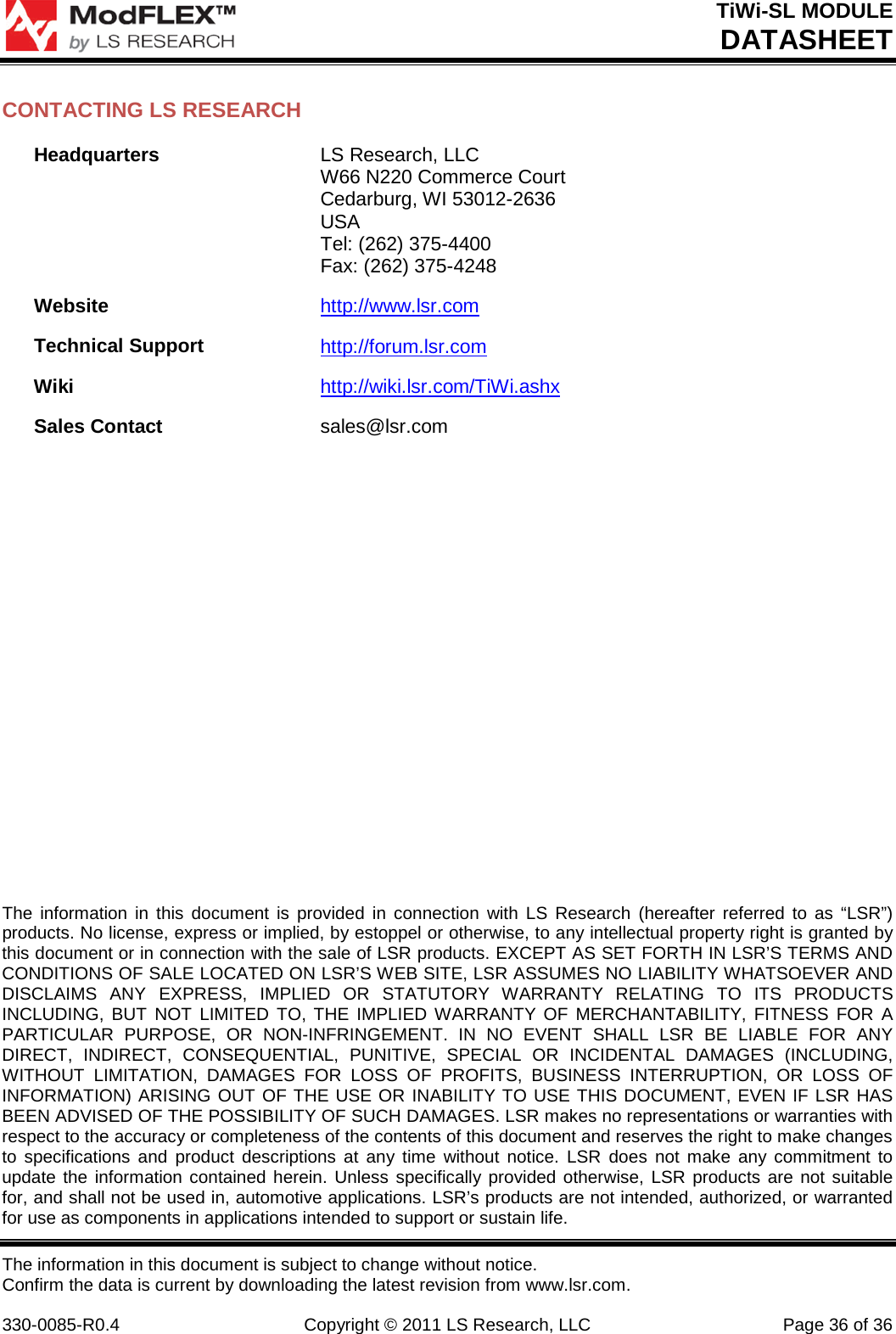
![TiWi-SL MODULE DATASHEET The information in this document is subject to change without notice. Confirm the data is current by downloading the latest revision from www.lsr.com. 330-0085-R0.4 Copyright © 2011 LS Research, LLC Page 12 of 36 Power Consumption - WLAN Parameter Test Conditions Min Typical Max Unit CCK (b) TX Current 2437 MHz, VCC=3.3V, Tamb=+25°C Po=20 dBm, 11 Mbps CCK L=1200 bytes, tdelay (idle)=4 µS. - 280 - mA OFDM (g) TX Current 2437 MHz, VCC=3.3V, Tamb=+25°C Po=14.5 dBm, 54 Mbps OFDM L=1200 bytes, tdelay (idle)=4 µS. - 185 - mA CCK (b) RX Current - 100 - mA OFDM (g) RX Current - 100 - mA Dynamic Mode [1] - <1.2 - mA Table 7: WLAN Power Consumption [1] Total Current from VCC for reception of Beacons with DTIM=1 TBTT=100 mS, Beacon duration 1.6ms, 1 Mbps beacon reception in Listen Mode.](https://usermanual.wiki/Laird-Connectivity/TIWISL01/User-Guide-1600739-Page-12.png)
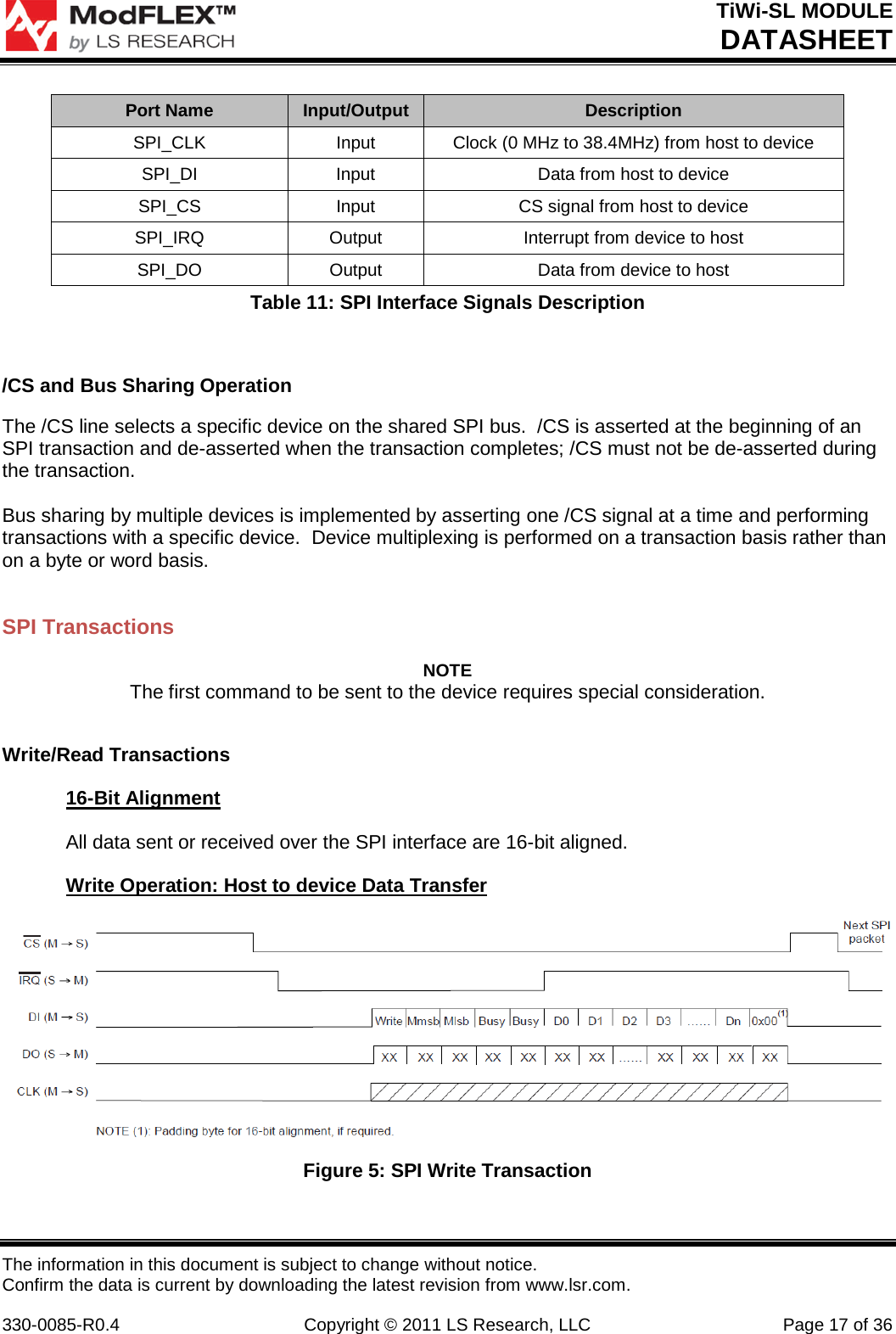
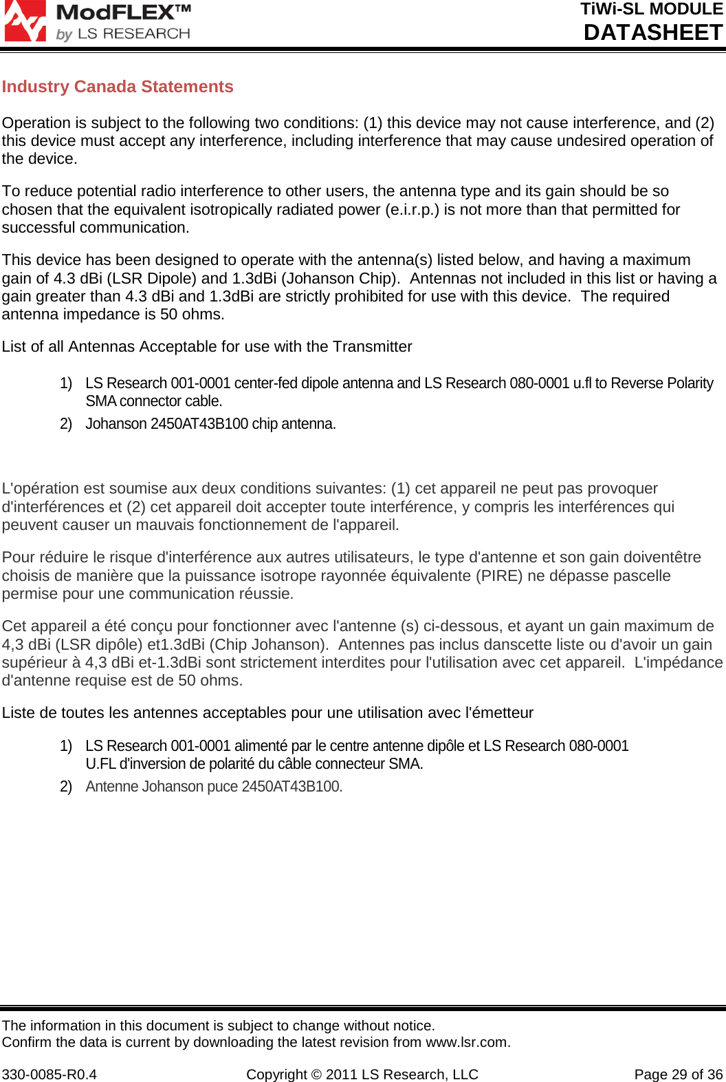
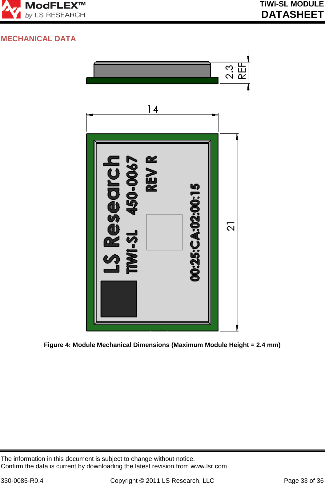
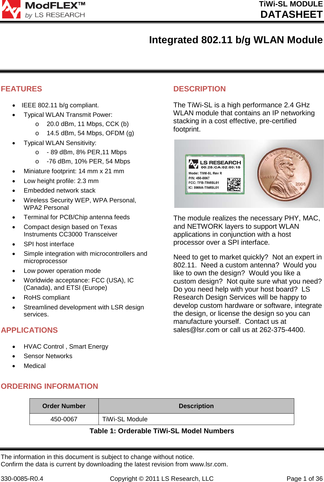
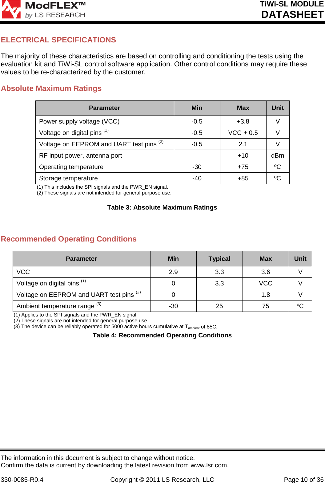
![TiWi-SL MODULE DATASHEET The information in this document is subject to change without notice. Confirm the data is current by downloading the latest revision from www.lsr.com. 330-0085-R0.4 Copyright © 2011 LS Research, LLC Page 14 of 36 WLAN Receiver Characteristics (TA =25°C, VCC=3.3V) [1] Parameter Test Conditions Min Typ Max Unit 1 Mbps CCK (b) RX Sensitivity 8% PER - -97 - dBm 11 Mbps CCK (b) RX Sensitivity 8% PER - -89 - dBm 9 Mbps OFDM (g) RX Sensitivity 10% PER - -90 - dBm 54 Mbps OFDM (g) RX Sensitivity 10% PER - -76 - dBm 11 Mbps CCK (b) RX Overload Level. 8% PER -10 - - dBm 6 Mbps OFDM (g) RX Overload Level. 10% PER -20 - - dBm 54 Mbps OFDM (g) RX Overload Level. 10% PER -20 - - dBm [1] Up to 2 dB degradation at Channel 13 for 11g modes and up to 2 dB degradation at Channel 14 for 11b/g modes. Table 9: WLAN Receiver RF Characteristics](https://usermanual.wiki/Laird-Connectivity/TIWISL01/User-Guide-1600739-Page-14.png)