Laird Connectivity TIWISL01 TiWi-SL User Manual
LS Research, LLC TiWi-SL
User Manual
TiWi-SL MODULE
DATASHEET
The information in this document is subject to change without notice.
Confirm the data is current by downloading the latest revision from www.lsr.com.
330-0085-R0.4 Copyright © 2011 LS Research, LLC Page 1 of 36
Integrated 802.11 b/g WLAN Module
FEATURES
• IEEE 802.11 b/g compliant.
• Typical WLAN Transmit Power:
o 20.0 dBm, 11 Mbps, CCK (b)
o 14.5 dBm, 54 Mbps, OFDM (g)
• Typical WLAN Sensitivity:
o - 89 dBm, 8% PER,11 Mbps
o -76 dBm, 10% PER, 54 Mbps
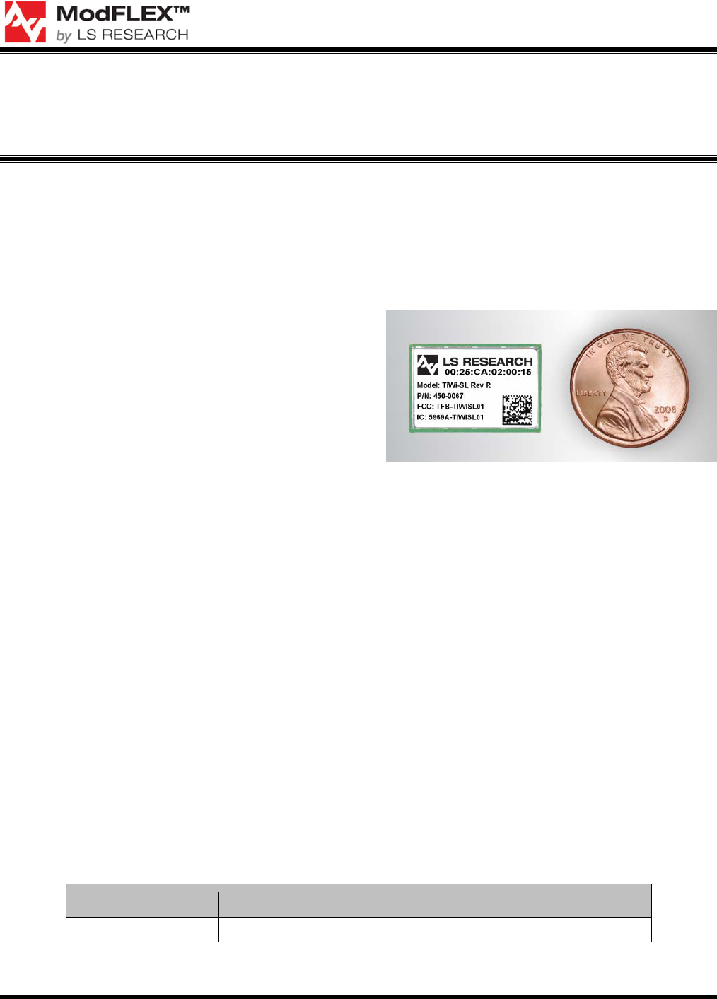
• Miniature footprint: 14 mm x 21 mm
• Low height profile: 2.3 mm
• Embedded network stack
• Wireless Security WEP, WPA Personal,
WPA2 Personal
• Terminal for PCB/Chip antenna feeds
• Compact design based on Texas
Instruments CC3000 Transceiver
• SPI host interface
• Simple integration with microcontrollers and
microprocessor
• Low power operation mode
• Worldwide acceptance: FCC (USA), IC
(Canada), and ETSI (Europe)
• RoHS compliant
• Streamlined development with LSR design
services.
APPLICATIONS
• HVAC Control , Smart Energy
• Sensor Networks
• Medical
DESCRIPTION
The TiWi-SL is a high performance 2.4 GHz
WLAN module that contains an IP networking
stacking in a cost effective, pre-certified
footprint.
The module realizes the necessary PHY, MAC,
and NETWORK layers to support WLAN
applications in conjunction with a host
processor over a SPI interface.
Need to get to market quickly? Not an expert in
802.11. Need a custom antenna? Would you
like to own the design? Would you like a
custom design? Not quite sure what you need?
Do you need help with your host board? LS
Research Design Services will be happy to
develop custom hardware or software, integrate
the design, or license the design so you can
manufacture yourself. Contact us at
sales@lsr.com or call us at 262-375-4400.
ORDERING INFORMATION
Order Number
Description
450-0067
TiWi-SL Module
Table 1: Orderable TiWi-SL Model Numbers
TiWi-SL MODULE
DATASHEET
The information in this document is subject to change without notice.
Confirm the data is current by downloading the latest revision from www.lsr.com.
330-0085-R0.4 Copyright © 2011 LS Research, LLC Page 2 of 36
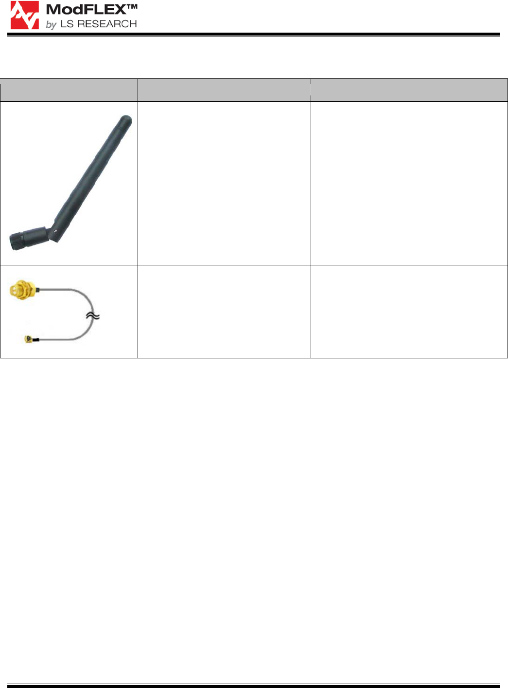
MODULE ACCESSORIES
Order Number
Description
001-0001 2.4 GHz Dipole Antenna with Reverse
Polarity SMA Connector
080-0001 u.fl to Reverse Polarity SMA Bulkhead
Cable 105mm
TiWi-SL MODULE
DATASHEET
The information in this document is subject to change without notice.
Confirm the data is current by downloading the latest revision from www.lsr.com.
330-0085-R0.4 Copyright © 2011 LS Research, LLC Page 3 of 36
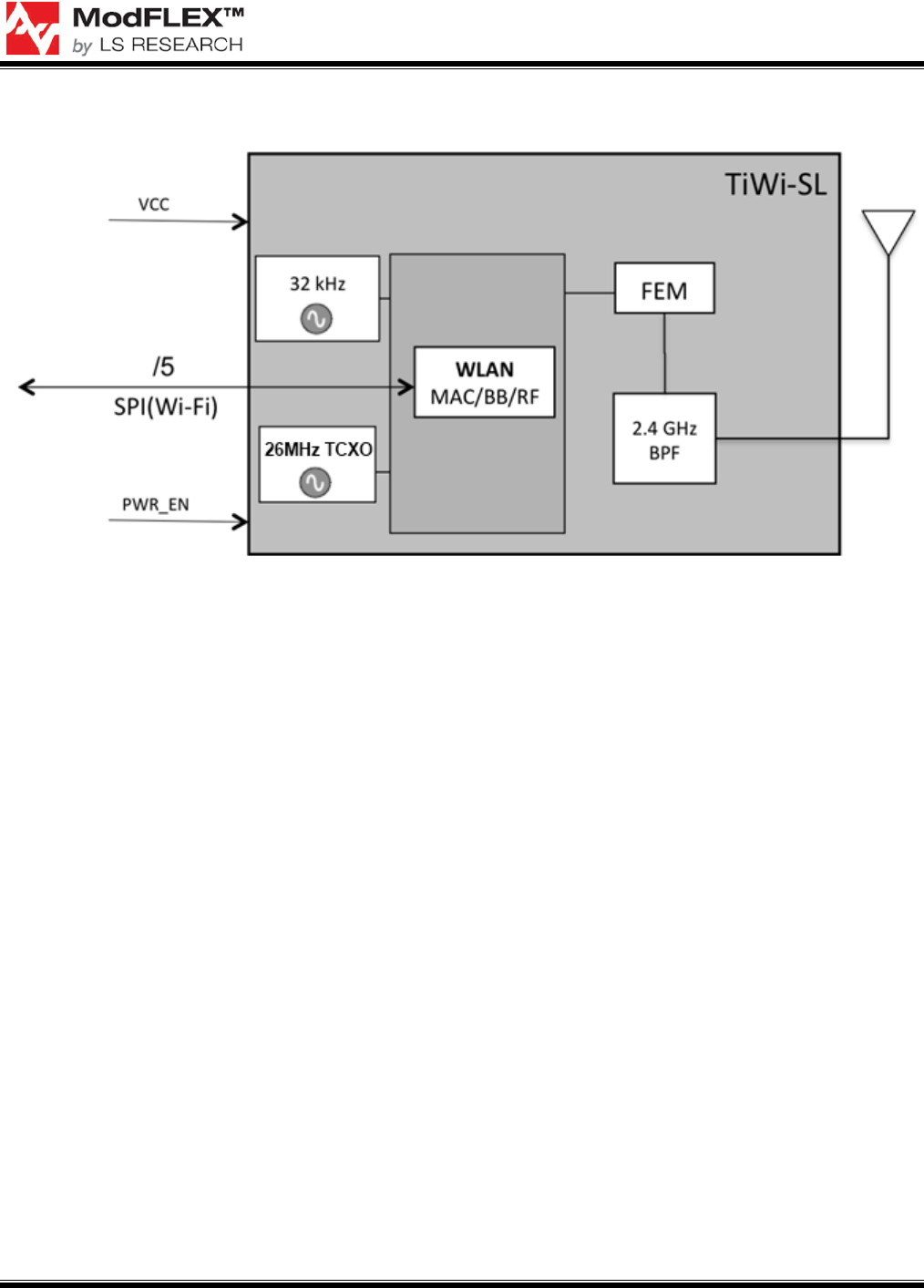
BLOCK DIAGRAM
Figure 1: TiWi-SL Module Block Diagram – Top-Level

TiWi-SL MODULE
DATASHEET
The information in this document is subject to change without notice.
Confirm the data is current by downloading the latest revision from www.lsr.com.
330-0085-R0.4 Copyright © 2011 LS Research, LLC Page 4 of 36
FUNCTIONAL BLOCK FEATURES
WLAN Features
• WLAN MAC Baseband Processor and RF transceiver which is IEEE802.11b/g compliant
• Accepts 26MHz reference clock Input
• IEEE Std 802.11d,i PICS compliant
• Supports serial debug interface
• Supports Serial Peripheral Interface (SPI) Host Interface
• Medium-Access Controller (MAC)
o Embedded ARM™ Central Processing Unit (CPU)
o Hardware-Based Encryption/Decryption Using 64-, 128-Bit WEP, TKIP or AES Keys,
o Supports requirements for Wireless Fidelity (Wi-Fi) Protected Access (WPA and
WPA2.0) and IEEE
o Std 802.11i [Includes Hardware-Accelerated Advanced-Encryption Standard (AES)]
• Baseband Processor
• 2.4GHz Radio
o Digital Radio Processor (DRP) implementation
o Internal LNA
o Supports : IEEE Std 802.11b, 802.11g, 802.11b/g
Network Stack Supported Protocols
• Transport layer:
o TCP
o UDP
• Network layer:
o IPv4
o Ping
o DHCP
o DNS Client
• Link layer:
o ARP
Wireless Security System Features
• Supported modes:
o Open (no security)
o WEP
o WPA-personal
o WPA2-personal
• Supported encryption types:
o WEP
o TKIP
o AES
o Open

TiWi-SL MODULE
DATASHEET
The information in this document is subject to change without notice.
Confirm the data is current by downloading the latest revision from www.lsr.com.
330-0085-R0.4 Copyright © 2011 LS Research, LLC Page 5 of 36
TABLE OF CONTENTS
FEATURES .......................................................................................................................... 1
APPLICATIONS ................................................................................................................... 1
DESCRIPTION ..................................................................................................................... 1
ORDERING INFORMATION ................................................................................................ 1
MODULE ACCESSORIES ................................................................................................... 2
BLOCK DIAGRAM ............................................................................................................... 3
FUNCTIONAL BLOCK FEATURES .................................................................................... 4
WLAN Features ........................................................................................................................................... 4
Network Stack Supported Protocols ......................................................................................................... 4
Wireless Security System Features .......................................................................................................... 4
TIWI-SL MODULE FOOTPRINT AND PIN DEFINITIONS ................................................... 7
PIN DESCRIPTIONS ............................................................................................................ 8
ELECTRICAL SPECIFICATIONS ...................................................................................... 10
Absolute Maximum Ratings ..................................................................................................................... 10
Recommended Operating Conditions .................................................................................................... 10
General Characteristics ............................................................................................................................ 11
WLAN RF Characteristics......................................................................................................................... 13
DEVICE POWER-UP AND ENABLE ................................................................................. 15
SPI HOST-CONTROLLER INTERFACE ........................................................................... 16
Overview .................................................................................................................................................... 16
Supported SPI Features ........................................................................................................................... 16
SPI Interface Description .......................................................................................................................... 16
SPI Transactions ....................................................................................................................................... 17
SOLDERING RECOMMENDATIONS ................................................................................ 26
Recommended Reflow Profile for Lead Free Solder ............................................................................. 26
CLEANING ......................................................................................................................... 27
OPTICAL INSPECTION ..................................................................................................... 27
REWORK ........................................................................................................................... 27

TiWi-SL MODULE
DATASHEET
The information in this document is subject to change without notice.
Confirm the data is current by downloading the latest revision from www.lsr.com.
330-0085-R0.4 Copyright © 2011 LS Research, LLC Page 6 of 36
SHIPPING, HANDLING, AND STORAGE ......................................................................... 27
Shipping ..................................................................................................................................................... 27
Handling ..................................................................................................................................................... 27
Moisture Sensitivity Level (MSL) ............................................................................................................. 27
Storage ....................................................................................................................................................... 27
Repeating Reflow Soldering .................................................................................................................... 27
AGENCY CERTIFICATIONS ............................................................................................. 28
AGENCY STATEMENTS ................................................................................................... 28
Federal Communication Commission Interference Statement ............................................................ 28
Industry Canada Statements.................................................................................................................... 29
OEM RESPONSIBILITIES TO COMPLY WITH FCC AND INDUSTRY CANADA
REGULATIONS ....................................................................................................... 30
OEM LABELING REQUIREMENTS FOR END-PRODUCT .............................................. 31
OEM END PRODUCT USER MANUAL STATEMENTS.................................................... 32
MECHANICAL DATA......................................................................................................... 33
DEVICE MARKINGS .......................................................................................................... 35
Rev 1 Devices ............................................................................................................................................ 35
CONTACTING LS RESEARCH ......................................................................................... 36
TiWi-SL MODULE
DATASHEET
The information in this document is subject to change without notice.
Confirm the data is current by downloading the latest revision from www.lsr.com.
330-0085-R0.4 Copyright © 2011 LS Research, LLC Page 7 of 36
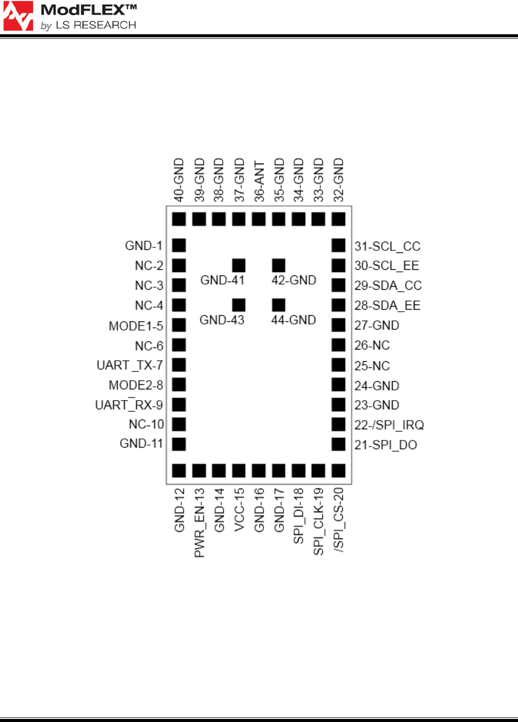
TIWI-SL MODULE FOOTPRINT AND PIN DEFINITIONS
To apply the TiWi-SL module, it is important to use the module pins in your application as they are
designated below, and in the corresponding pin definition table found on pages 7 and 8. Not all the
pins on the TiWi-SL module may be used, as some are reserved.
Figure 2: TiWi-SL Pinout
TiWi-SL MODULE
DATASHEET
The information in this document is subject to change without notice.
Confirm the data is current by downloading the latest revision from www.lsr.com.
330-0085-R0.4 Copyright © 2011 LS Research, LLC Page 8 of 36
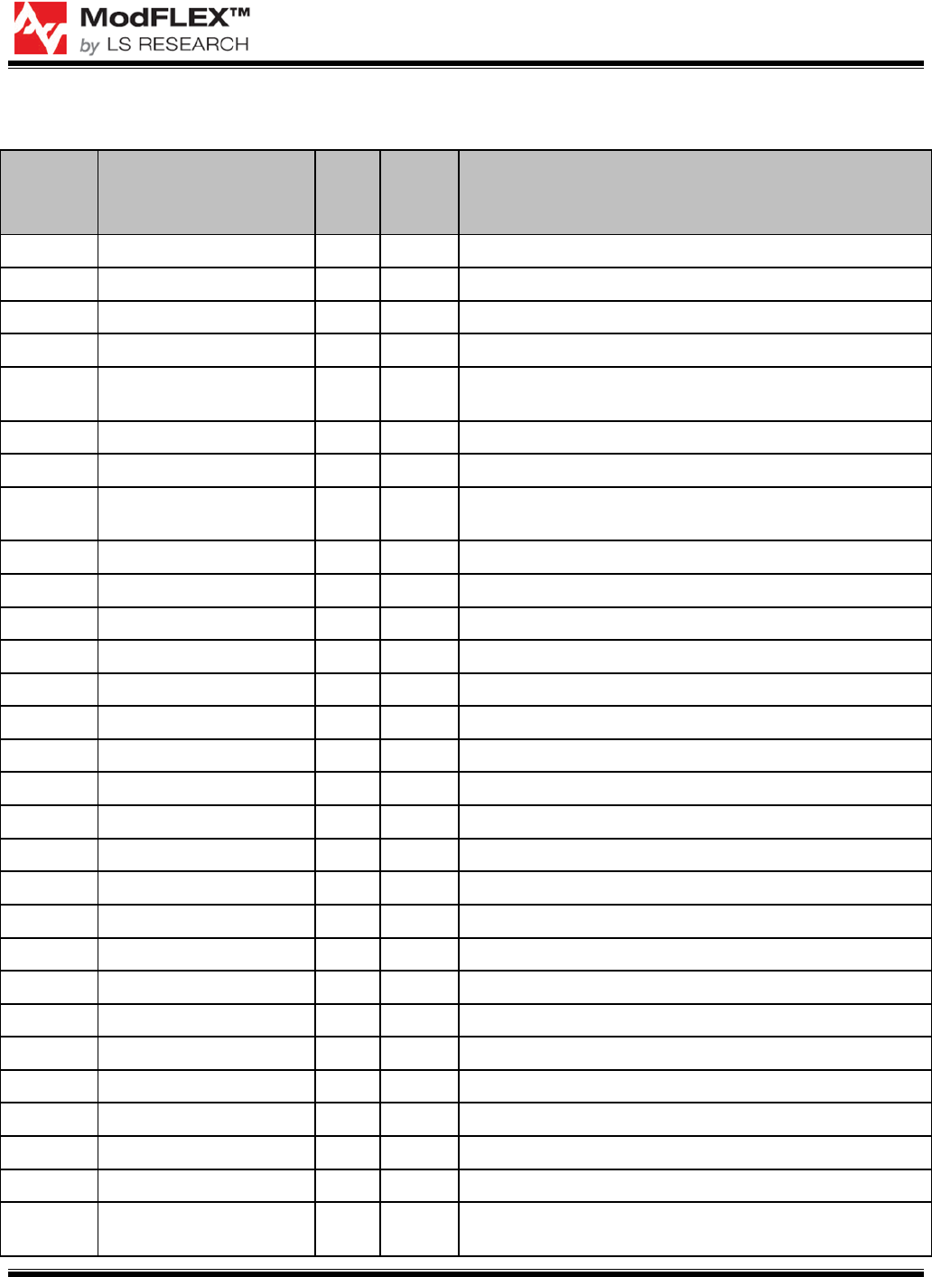
PIN DESCRIPTIONS
Module
Pin Name
I/O
Type
Buffer
Type Description
1
GND
GND
-
GROUND
2
NC
-
-
NO CONNECT (DO NOT CONNECT)
3
NC
-
-
NO CONNECT (DO NOT CONNECT)
4
NC
-
-
NO CONNECT (DO NOT CONNECT)
5 MODE1 DI - MODE1 (SHORT TO MODE2 FOR NORMAL USE,
SHORT TO GROUND FOR TEST USE)
6
NC
-
-
NO CONNECT (DO NOT CONNECT)
7
UART_TX (1)
DO
-
TEST UART TX (1.8V LOGIC)
8 MODE2 DI -
MODE2 (SHORT TO MODE1 FOR NORMAL USE,
LEAVE OPEN FOR TEST USE)
9
UART_RX (1)
DI
-
TEST UART RX (1.8V LOGIC)
10
NC
-
-
NO CONNECT (DO NOT CONNECT)
11
GND
GND
-
GROUND
12
GND
GND
-
GROUND
13
PWR_EN
DI
-
MODULE POWER ENABLE
14
GND
GND
-
GROUND
15
VCC
PI
-
POWER TO MODULE
16
GND
GND
-
GROUND
17
GND
GND
-
GROUND
18
SPI_DI
DI
8mA
HOST INTERFACE SPI DATA IN
19
SPI_CLK
DI
4mA
HOST INTERFACE SPI CLOCK
20
/SPI_CS
DI
4mA
HOST INTERFACE SPI CHIP SELECT (ACTIVE LOW)
21
SPI_DO
DO
8mA
HOST INTERFACE SPI DATA OUT
22
/SPI_IRQ
DO
4mA
HOST INTERFACE SPI INTERRUPT (ACTIVE LOW)
23
GND
GND
-
GROUND
24
GND
GND
-
GROUND
25
NC
-
-
NO CONNECT (DO NOT CONNECT)
26
NC
-
-
NO CONNECT (DO NOT CONNECT)
27
GND
GND
-
GROUND
28
SDA_EE (2)
DIO
-
I2C DATA LINE FROM EEPROM (1.8V LOGIC)
29 SDA_CC (2) DIO 4mA
I2C DATA LINE FROM CC3000, PULL-UP ON
MODULE (1.8V LOGIC)
TiWi-SL MODULE
DATASHEET
The information in this document is subject to change without notice.
Confirm the data is current by downloading the latest revision from www.lsr.com.
330-0085-R0.4 Copyright © 2011 LS Research, LLC Page 9 of 36
Module
Pin Name
I/O
Type
Buffer
Type Description
30
SCL_EE (3)
DI
-
I2C CLOCK LINE FROM EEPROM (1.8V LOGIC)
31 SCL_CC (3) DO 4mA
I2C CLOCK LINE FROM CC3000, PULL-UP ON
MODULE (1.8V LOGIC)
32
GND
GND
-
GROUND
33
GND
GND
-
GROUND
34
GND
GND
-
GROUND
35
GND
GND
-
GROUND
36
ANT (4)
RF
-
ANTENNA, 50 OHMS
37
GND
GND
-
GROUND
38
GND
GND
-
GROUND
39
GND
GND
-
GROUND
40
GND
GND
-
GROUND
41
GND
GND
-
GROUND
42
GND
GND
-
GROUND
43
GND
GND
-
GROUND
44
GND
GND
-
GROUND
(1) These signals are test UART signals which are 1.8v logic, and they should be left unconnected for normal operation.
(2) The I2C data signals from the CC3000 and EEPROM must be connected together for normal operation.
(3) The I2C clock signals from the CC3000 and EEPROM must be connected together for normal operation.
(4) The antenna terminal presents a DC short circuit to ground.
PI = Power Input
DI = Digital Input
DO = Digital Output
DIO = Bi-directional Digital Port
RF = Bi-directional RF Port
GND=Ground
Table 2: TiWi-SL Module Pin Descriptions
TiWi-SL MODULE
DATASHEET
The information in this document is subject to change without notice.
Confirm the data is current by downloading the latest revision from www.lsr.com.
330-0085-R0.4 Copyright © 2011 LS Research, LLC Page 10 of 36
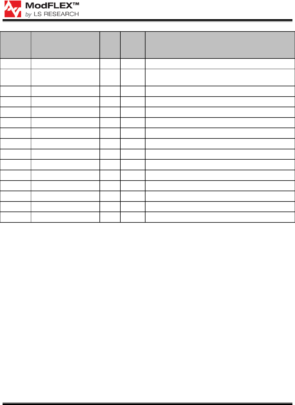
ELECTRICAL SPECIFICATIONS
The majority of these characteristics are based on controlling and conditioning the tests using the
evaluation kit and TiWi-SL control software application. Other control conditions may require these
values to be re-characterized by the customer.
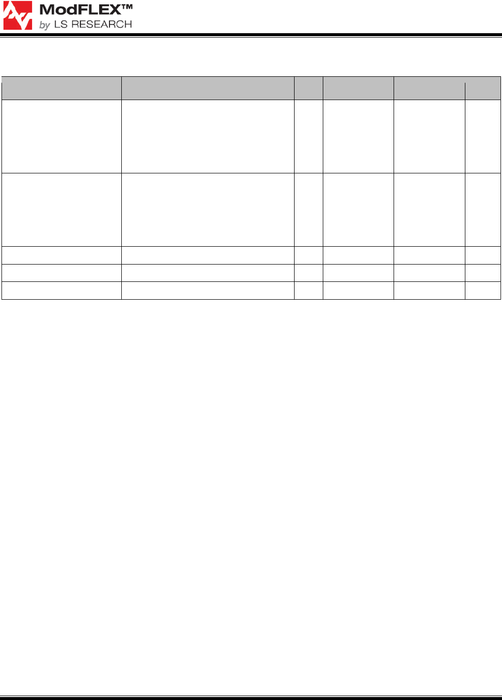
Absolute Maximum Ratings
Parameter
Min
Max
Unit
Power supply voltage (VCC)
-0.5
+3.8
V
Voltage on digital pins (1)
-0.5
VCC + 0.5
V
Voltage on EEPROM and UART test pins (2)
-0.5
2.1
V
RF input power, antenna port
+10
dBm
Operating temperature
-30
+75
ºC
Storage temperature
-40
+85
ºC
(1) This includes the SPI signals and the PWR_EN signal.
(2) These signals are not intended for general purpose use.
Table 3: Absolute Maximum Ratings
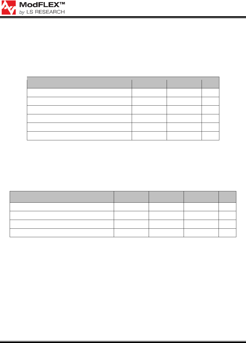
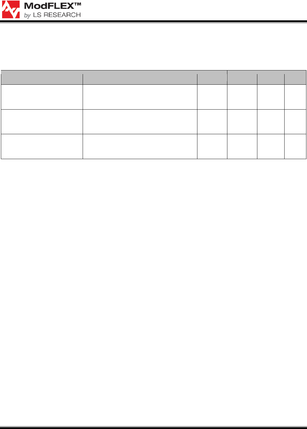
Recommended Operating Conditions
Parameter
Min
Typical
Max
Unit
VCC
2.9
3.3
3.6
V
Voltage on digital pins (1)
0
3.3
VCC
V
Voltage on EEPROM and UART test pins (2)
0
1.8
V
Ambient temperature range (3)
-30
25
75
ºC
(1) Applies to the SPI signals and the PWR_EN signal.
(2) These signals are not intended for general purpose use.
(3) The device can be reliably operated for 5000 active hours cumulative at Tambient of 85C.
Table 4: Recommended Operating Conditions
TiWi-SL MODULE
DATASHEET
The information in this document is subject to change without notice.
Confirm the data is current by downloading the latest revision from www.lsr.com.
330-0085-R0.4 Copyright © 2011 LS Research, LLC Page 11 of 36
General Characteristics
DC Characteristics – General Purpose I/O
Parameter
Test Conditions
Min
Typical
Max
Unit
Logic input low, VIL
0
-
0.8
V
Logic input high, VIH
2.0
-
VCC
V
Logic output low, VOL
8mA
0
-
.55
V
Logic output high, VOH
8mA
2.0
-
VCC
V
Applies to the SPI signals and the PWR_EN signal.
Table 5: DC Characteristics General Purpose I/O
RF Characteristics
Parameter
Min
Typical
Max
Unit
RF frequency range
2412
2472
MHz
RF data rate 1
802.11 b/g
rates supported
54 Mbps
Table 6: RF Characteristics
TiWi-SL MODULE
DATASHEET
The information in this document is subject to change without notice.
Confirm the data is current by downloading the latest revision from www.lsr.com.
330-0085-R0.4 Copyright © 2011 LS Research, LLC Page 12 of 36
Power Consumption - WLAN
Parameter
Test Conditions
Min
Typical
Max
Unit
CCK (b) TX Current
2437 MHz, VCC=3.3V, T
amb
=+25°C
Po=20 dBm, 11 Mbps CCK
L=1200 bytes, tdelay (idle)=4 µS.
- 280 - mA
OFDM (g) TX Current
2437 MHz, VCC=3.3V, T
amb
=+25°C
Po=14.5 dBm, 54 Mbps OFDM
L=1200 bytes, tdelay (idle)=4 µS.
- 185 - mA
CCK (b) RX Current
-
100
-
mA
OFDM (g) RX Current
-
100
-
mA
Dynamic Mode [1]
-
<1.2
-
mA
Table 7: WLAN Power Consumption
[1] Total Current from VCC for reception of Beacons with DTIM=1 TBTT=100 mS, Beacon duration
1.6ms, 1 Mbps beacon reception in Listen Mode.
TiWi-SL MODULE
DATASHEET
The information in this document is subject to change without notice.
Confirm the data is current by downloading the latest revision from www.lsr.com.
330-0085-R0.4 Copyright © 2011 LS Research, LLC Page 13 of 36
WLAN RF Characteristics
WLAN Transmitter Characteristics
(TA =25°C, VCC=3.3 V)
Parameter
Test Conditions
Min
Typ
Max
Unit
11 Mbps CCK (b) TX
Output Power
11 Mbps CCK , 802.11(b) Mask
Compliance, 35% EVM
RMS power over TX packet
- 20 - dBm
9 Mbps OFDM (g) TX
Output Power
9 Mbps OFDM , 802.11(g) Mask
Compliance, -8 dB EVM
RMS power over TX packet
- 19 - dBm
54 Mbps OFDM (g) TX
Output Power
54 Mbps OFDM, 802.11(g) Mask
Compliance, -25 dB EVM
RMS power over TX packet
- 14.5 - dBm
Table 8: WLAN Transmitter RF Characteristics
TiWi-SL MODULE
DATASHEET
The information in this document is subject to change without notice.
Confirm the data is current by downloading the latest revision from www.lsr.com.
330-0085-R0.4 Copyright © 2011 LS Research, LLC Page 14 of 36
WLAN Receiver Characteristics
(TA =25°C, VCC=3.3V) [1]
Parameter
Test Conditions
Min
Typ
Max
Unit
1 Mbps CCK (b) RX
Sensitivity
8% PER - -97 - dBm
11 Mbps CCK (b) RX
Sensitivity
8% PER - -89 - dBm
9 Mbps OFDM (g) RX
Sensitivity
10% PER - -90 - dBm
54 Mbps OFDM (g) RX
Sensitivity
10% PER - -76 - dBm
11 Mbps CCK (b) RX
Overload Level.
8% PER -10 - - dBm
6 Mbps OFDM (g) RX
Overload Level.
10% PER -20 - - dBm
54 Mbps OFDM (g) RX
Overload Level.
10% PER -20 - - dBm
[1] Up to 2 dB degradation at Channel 13 for 11g modes and up to 2 dB degradation at Channel 14 for
11b/g modes.
Table 9: WLAN Receiver RF Characteristics
TiWi-SL MODULE
DATASHEET
The information in this document is subject to change without notice.
Confirm the data is current by downloading the latest revision from www.lsr.com.
330-0085-R0.4 Copyright © 2011 LS Research, LLC Page 15 of 36
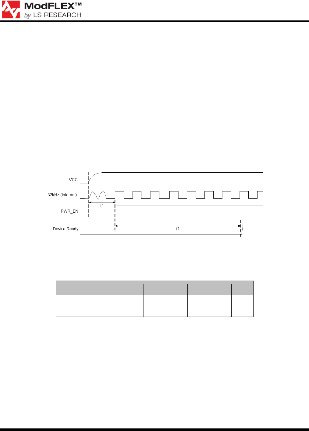
DEVICE POWER-UP AND ENABLE
Normal operation mode requirements:
1. The MODE1 and MODE2 signals need to be shorted together.
The following sequence describes the device power-up from shutdown. See Figure 3 and Table 10 for timing
details.
Normal operation power-up requirements:
1. Apply power to the module through the VCC input.
2. Wait for the internal 32kHz clock to start-up and stabilize (t1).
3. Enable the module through the PWR_EN input.
4. Wait for the module to start-up and be ready (t2).
Figure 3: Device Power-Up Timing
Timing Parameter
Symbol
Max
Unit
VCC to PWR_EN
t1
???
msec
PWR_EN to Device Ready
t2
???
Msec
Table 10: Device Power-Up Timing
TiWi-SL MODULE
DATASHEET
The information in this document is subject to change without notice.
Confirm the data is current by downloading the latest revision from www.lsr.com.
330-0085-R0.4 Copyright © 2011 LS Research, LLC Page 16 of 36
SPI HOST-CONTROLLER INTERFACE
This section describes the Serial Peripheral Interface ( SPI™) Host-Controller interface (HCI).
Overview
The SPI interface provides high-speed data transfer capability with low power consumption for mobile
electronic devices. The SPI bus was designed to operate on a point-to-multipoint basis by providing a
separate, active-low chip select (CS) per device.
Supported SPI Features
SPI supports the following features:
• Point-to-multipoint
• Supported clock rates = 26MHz and 38.4MHz
• The device interface is always an SPI Slave, host is always an SPI Master
SPI Interface Description
In order to facilitate a broad implementation, the protocol is half duplex and does not require
simultaneous operation of data OUT (DO) and data IN (DI). All TI communication devices are slaves in
this protocol, and all transactions are initiated by the host, as the SPI Master. The clock rate for each
one of the connected devices may be different and configured per device.
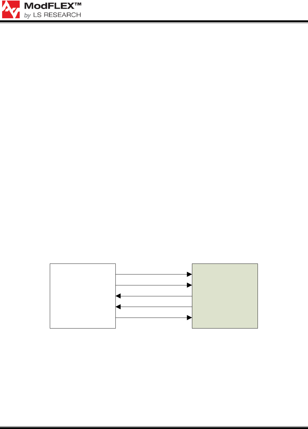
Figure 4 illustrates the SPI interface signals; Table 11 describes the SPI interface signals.
Host Device
SPI_CLK
SPI_CS
SPI_IRQ
SPI_DO (Data Out)
SPI_DI (Data In)
Figure 4: SPI Interface Signals
TiWi-SL MODULE
DATASHEET
The information in this document is subject to change without notice.
Confirm the data is current by downloading the latest revision from www.lsr.com.
330-0085-R0.4 Copyright © 2011 LS Research, LLC Page 17 of 36
Port Name Input/Output Description
SPI_CLK Input Clock (0 MHz to 38.4MHz) from host to device
SPI_DI Input Data from host to device
SPI_CS Input CS signal from host to device
SPI_IRQ Output Interrupt from device to host
SPI_DO Output Data from device to host
Table 11: SPI Interface Signals Description
/CS and Bus Sharing Operation
The /CS line selects a specific device on the shared SPI bus. /CS is asserted at the beginning of an
SPI transaction and de-asserted when the transaction completes; /CS must not be de-asserted during
the transaction.
Bus sharing by multiple devices is implemented by asserting one /CS signal at a time and performing
transactions with a specific device. Device multiplexing is performed on a transaction basis rather than
on a byte or word basis.
SPI Transactions
NOTE
The first command to be sent to the device requires special consideration.
Write/Read Transactions
16-Bit Alignment
All data sent or received over the SPI interface are 16-bit aligned.
Write Operation: Host to device Data Transfer
Figure 5: SPI Write Transaction
TiWi-SL MODULE
DATASHEET
The information in this document is subject to change without notice.
Confirm the data is current by downloading the latest revision from www.lsr.com.
330-0085-R0.4 Copyright © 2011 LS Research, LLC Page 18 of 36
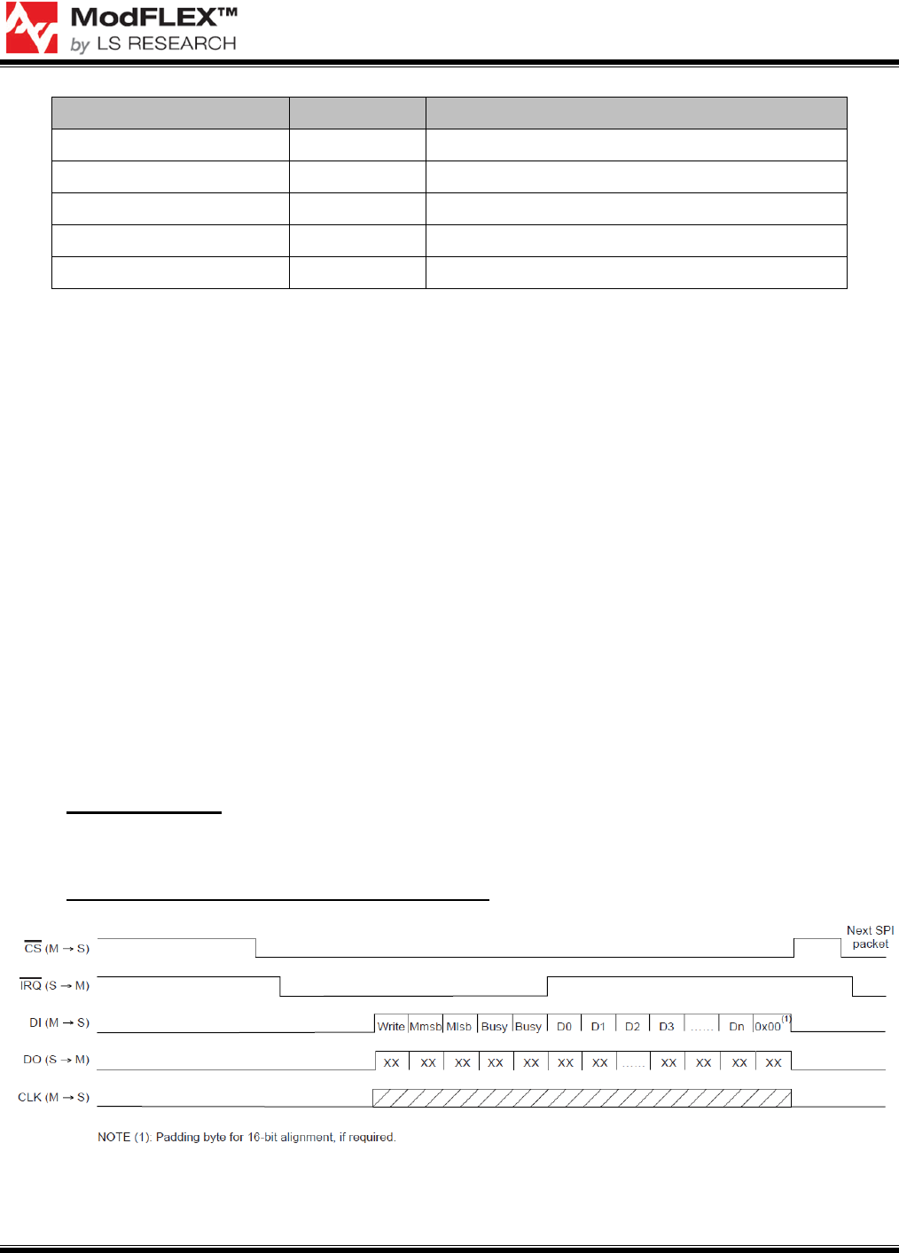
The host must assert /CS (that is, drive the signal to low) to indicate that it is about to write to the
device. Consequently, the device will assert the /IRQ line when it is ready to receive the data and after
completing its wake-up sequence. The host will wait for the /IRQ line to be asserted and then will start
driving the data on the DI line. Data on the DI line consist of a 5-byte header followed by the data
payload.
The first byte of the header is the WRITE opcode, followed by two bytes that indicate the size of the
payload length (including the alignment byte). Two BUSY bytes will then follow to conclude the header.
Directly following the last byte of the header will be the data payload.
When the device detects the HCI packet header, it de-asserts its /IRQ line during the packet data.
When the host completes the SPI transaction, it must de-assert its /CS line.
SPI Header: Write = Opcode for write is 0x01
MMSB, MLSB = 16-bit data payload length (including alignment byte)
Busy = Busy byte (0x00)
SPI Payload (equal to the HCI command + padding byte):
D(0) … D(n), 0x00 (depending on the number of bytes in SPI payload)
XX = Should be ignored by master
In order for the total SPI packet (that is, the SPI transaction) to be 16-bit aligned, the HCI command
must be padded with an additional 0x00 byte if the HCI packet is even size. Refer to Table 12 for more
information.
SPI Header SPI Payload Padding Byte
5 bytes Odd None
5 bytes Even 0x00
Table 12: SPI Read/Write Transaction: 16-bit Alignment
The write transaction is performed according to the following parameters:
• A complete HCI packet must be included within every SPI transaction.
• Pausing and resuming the SPI clock: the host may stop driving the SPI CLK during the SPI
packet. During this time, /CS will remain asserted. Upon resuming the SPI CLK the Host will
not send the header again and will simply continue driving the data from the point it was
previously stopped.
• The number of bytes for each SPI transaction is always even.
• The padding byte is added at the end of the HCI packet, but is not reflected in the HCI header
length parameter (H4 packet length ignores this byte).
• The device ignores the additional byte.
TiWi-SL MODULE
DATASHEET
The information in this document is subject to change without notice.
Confirm the data is current by downloading the latest revision from www.lsr.com.
330-0085-R0.4 Copyright © 2011 LS Research, LLC Page 19 of 36
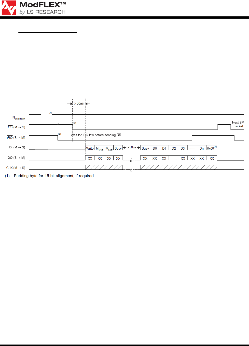
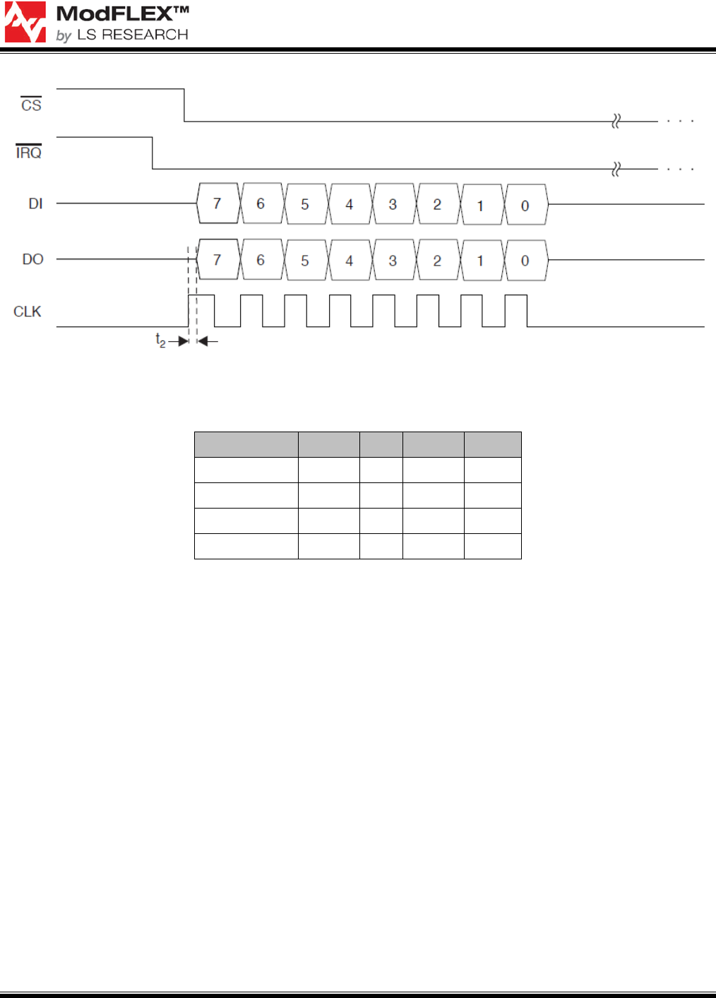
First Write Transaction
The first write transaction to occur after release of the shutdown has a slightly different timing
than the one shown in Figure 5. The normal SPI host write sequence is /CS low (host
device), followed by /IRQ low (device host), indicating that the device is ready to accept
data. However, after power-up, the sequence is slightly different, as Figure 6 illustrates.
After the release of the NSHUTDOWN pin (indicated by (A) in Figure 6 below), the /IRQ line will
assert (that is, go from high to low), as indicated by (B). The Host must wait for /IRQ to be low
before asserting /CS, as noted by (C). The Host must then wait for at least 50 μs from the
assertion of /CS (that is, 50 μs after /CS goes low) before sending the SPI packet.
Figure 6: Write First Transaction
In addition, during this command the device performs its internal processing to switch to the
required SPI mode. This processing requires an additional small amount of time. Therefore, for
the first command only, a short delay is required after the first four bytes and before the
following bytes. This delay must also be greater than 50 μs.
TiWi-SL MODULE
DATASHEET
The information in this document is subject to change without notice.
Confirm the data is current by downloading the latest revision from www.lsr.com.
330-0085-R0.4 Copyright © 2011 LS Research, LLC Page 20 of 36
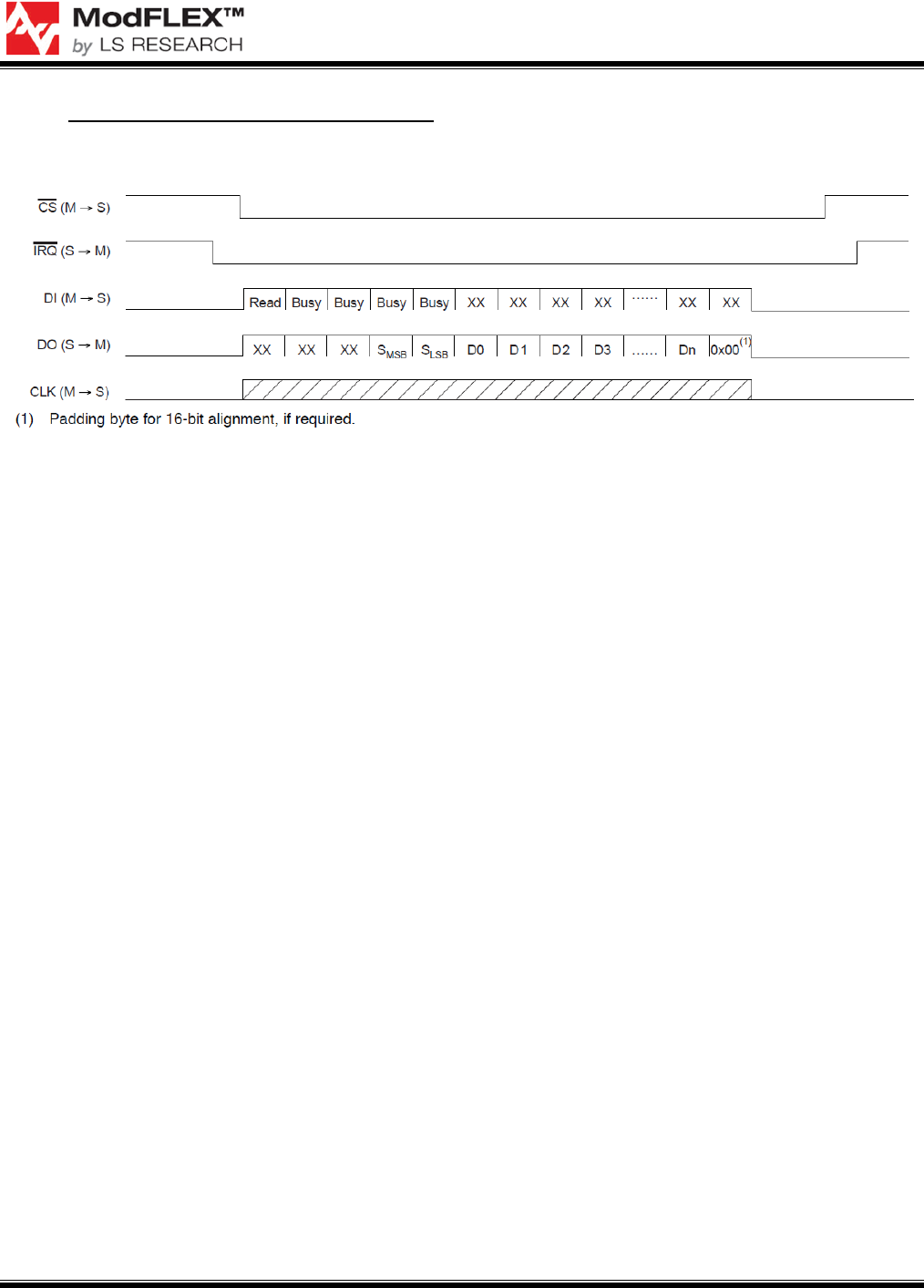
Read Operation: to Host Data Transfer
Figure 7 shows the SPI read transaction timing.
Figure 7: SPI Read Transaction
SPI Header: Read = Opcode for write is 0x03
SMSB, SLSB = 16-bit data payload length (including alignment byte)
Busy = Busy byte (0x00)
SPI Payload (equal to the HCI command + padding byte):
D(0) … D(n), 0x00 (depending on the number of bytes in SPI payload)
In order for the total SPI packet (that is, the SPI transaction) to be 16-bit aligned, the HCI event sent
from the device is padded with an additional 0x00 byte (if required). Refer to for more information. The
device signals to the host its desire to transfer data by asserting the /IRQ line. The host asserts /CS
and drives the following 3 bytes to DI line: READ opcode followed by two BUSY bytes. The device will
then drive the data on the DO line. The first two bytes will indicate the payload length, and immediately
after that, the data payload bytes will follow. Upon completing the read transaction, the host must de-
assert /CS. The Bluetooth device then de-asserts its /IRQ line immediately as a response (within ≤ 250
ns).
NOTE
The host interrupt input should be set to trigger on high to low edge.
The read transaction is performed according to the following parameters:
• A single SPI read transaction includes a full HCI packet.
• The number of bytes for each SPI transaction will always be even.
• The padded byte is added at the end of the HCI packet, but is not reflected in the HCI header
length parameter (H4 packet length ignores this byte).
• The host should read a full SPI packet (including the alignment byte) according to the SPI
packet length (SMSB and SLSB).
• The host must ignore the additional byte according to the HCI packet length.
Refer to Section “SPI Timing Information” for the SPI read and write timing diagrams.
TiWi-SL MODULE
DATASHEET
The information in this document is subject to change without notice.
Confirm the data is current by downloading the latest revision from www.lsr.com.
330-0085-R0.4 Copyright © 2011 LS Research, LLC Page 21 of 36
Clock Polarity
Data is sampled on the falling edge of the clock as shown in Figure 9.
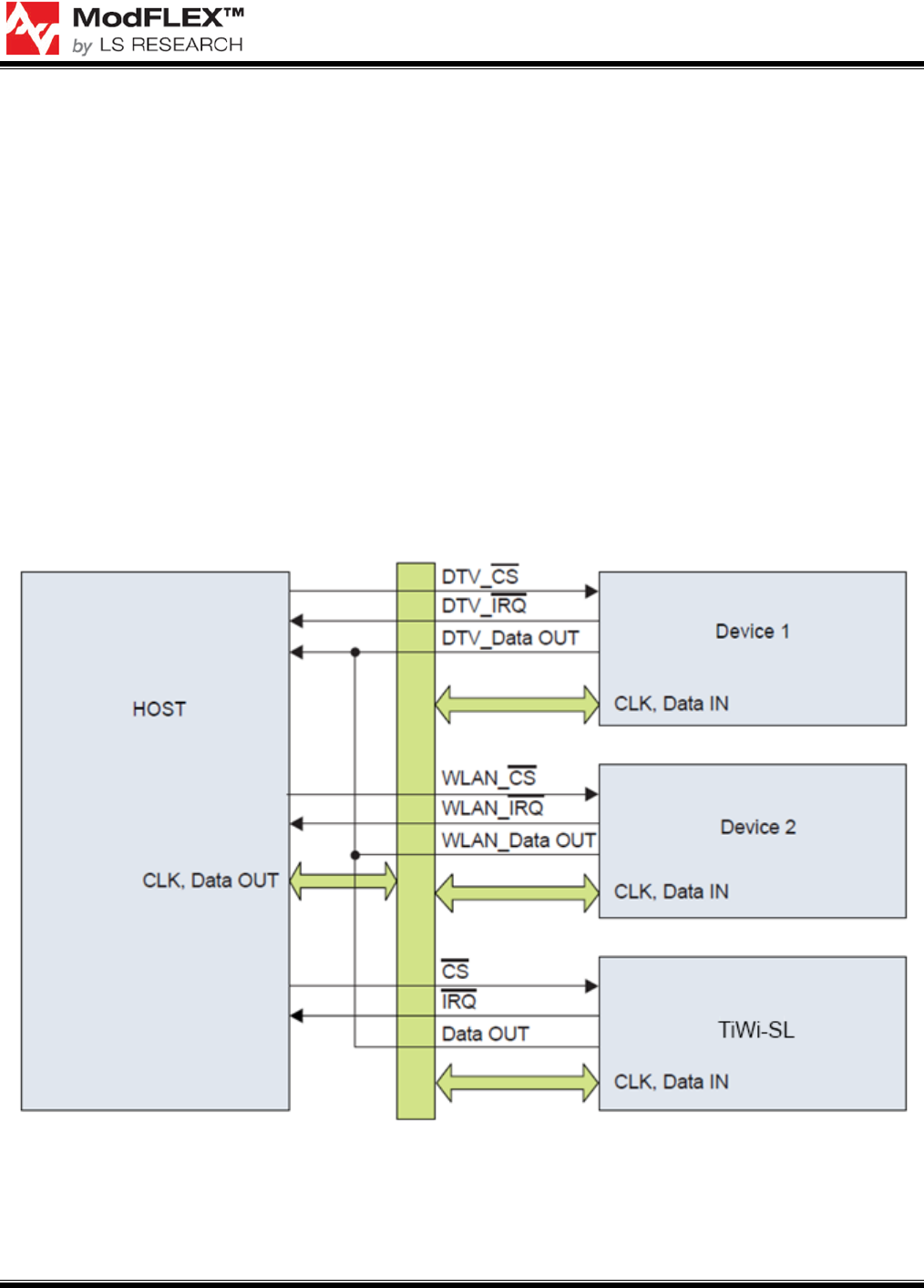
Shared SPI Bus Mode
This section describes the solution for a system in which the SPI host controller interfaces with other
SPI-compatible devices.
The topology includes one SPI master and an SPI bus shared by several slaves. The bus topology has
a single master (Host) and multiple slaves. The following lines are common to all SPI devices in the
system:
• CLK
• Data IN
• Data OUT—when this line is shared between the different devices, it must be set to go to a 3-
state output when /CS is de-asserted via the vendor-specific command,
HCI_VS_TI_SPI_Configuration (refer to TBD)
Figure 8 illustrates the shared SPI bus architecture, depicting three devices as examples.
Figure 8: Shared SPI Bus Topology
TiWi-SL MODULE
DATASHEET
The information in this document is subject to change without notice.
Confirm the data is current by downloading the latest revision from www.lsr.com.
330-0085-R0.4 Copyright © 2011 LS Research, LLC Page 22 of 36
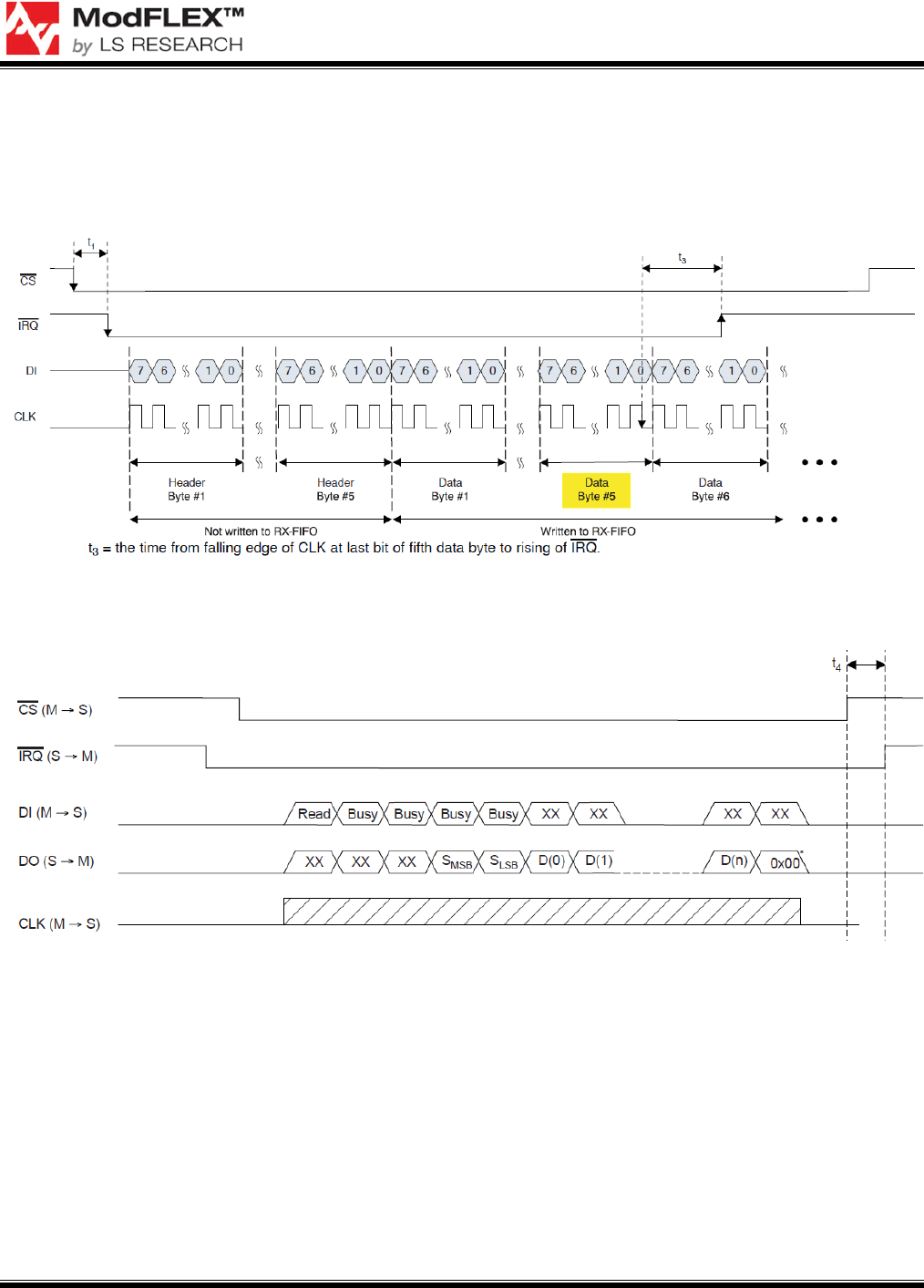
SPI Timing Information
Figure 9 through Figure 11 show the SPI write and read timing sequences, respectively. Figure 11 is
an expanded view of the first byte timing sequence for the SPI read header shown in Figure 10. Table
13 defines the SPI read/write timing parameters.
Figure 9: SPI Write Timing
Figure 10: SPI Read Transaction
TiWi-SL MODULE
DATASHEET
The information in this document is subject to change without notice.
Confirm the data is current by downloading the latest revision from www.lsr.com.
330-0085-R0.4 Copyright © 2011 LS Research, LLC Page 23 of 36
Figure 11: SPI Read Header: First Byte Timing
Time Min Typ Max Unit
t1 83 375 ns
t2 2.9 9.52 ns
t3 666 2125 ns
t4 83 375 ns
Table 13: SPI Read/Write Timing
TiWi-SL MODULE
DATASHEET
The information in this document is subject to change without notice.
Confirm the data is current by downloading the latest revision from www.lsr.com.
330-0085-R0.4 Copyright © 2011 LS Research, LLC Page 24 of 36
SPI Data Switching Characteristics
Parameter Min Max Unit
tCS Delay time, CS↓to DIN read/write command valid 0 clock cycles
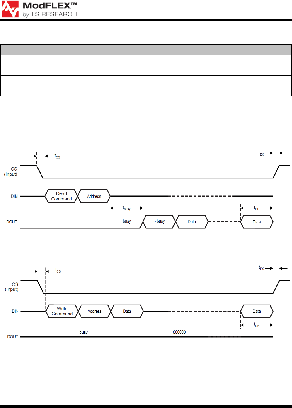
tbusy (1) Fixed busy delay till DOUT data valid 32 224 clock cycles
tEC Delay time, DOUT data valid to CS↑ 0 clock cycles
tDB (2) Data block size 32 clock cycles
Over recommended operating conditions (See Figure 12, Figure 13)
(1)The busy delay can be configured as fixed value after the address de-assertion. The values can be 1 to 7 (in multiples of 32 clock cycles).
(2) The data length can be configured as 16 or 32-bit words.
Table 14: SPI Data Switching Characteristics
Figure 12: SPI Interface Read Timing
Figure 13: SPI Interface Write Timing
TiWi-SL MODULE
DATASHEET
The information in this document is subject to change without notice.
Confirm the data is current by downloading the latest revision from www.lsr.com.
330-0085-R0.4 Copyright © 2011 LS Research, LLC Page 25 of 36
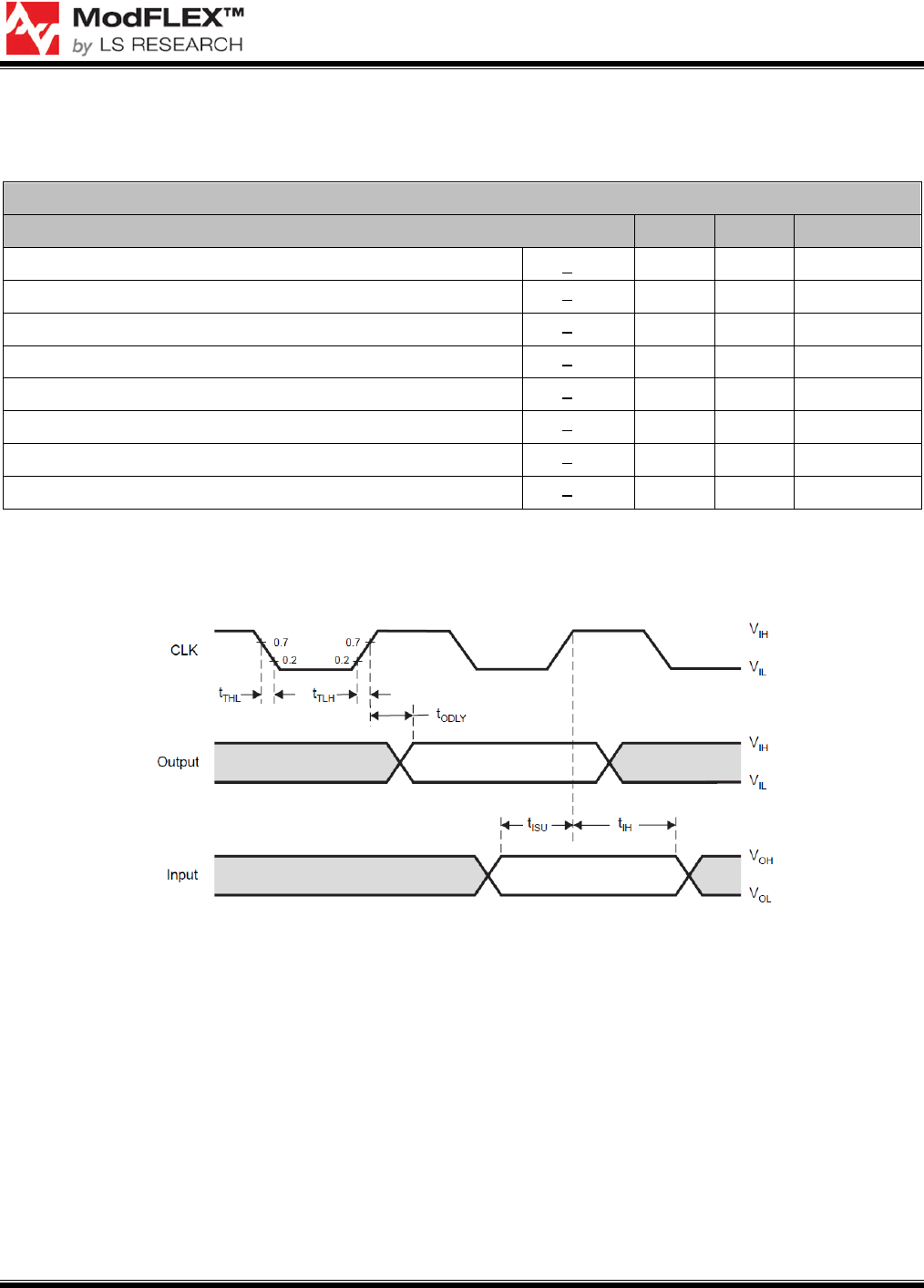
SPI Clock Switching Characteristics
This interface only supports single block reads and writes.
SPI/WSPI
Parameter Min Max Unit
fclock Clock frequency, CLK CL < 15pF 0 48 ns
DC Low/high duty cycle
C
L
< 15pF
40 60 ns
tTLH Rise time, CLK
C
L
< 15pF
4.3 ns
tTHL Fall time, CLK
C
L
< 15pF
3.5
ns
tISU Setup time, input valid before CLK↑
C
L
< 15pF
3.5
ns
tIH Hold time, input valid after CLK↑
C
L
< 15pF
5
ns
tODLY Setup time, input valid before CLK↑
C
L
< 15pF
4 15
ns
tsetupSPI_CSx CSn Delay time, CLK↑ to output invalid CL < 15pF
5.5 ns
Over recommended operating conditions (See Figure 14)
Table 15: SPI Clock Switching Characteristics
Figure 14: SPI Interface Clock Timing
TiWi-SL MODULE
DATASHEET
The information in this document is subject to change without notice.
Confirm the data is current by downloading the latest revision from www.lsr.com.
330-0085-R0.4 Copyright © 2011 LS Research, LLC Page 26 of 36
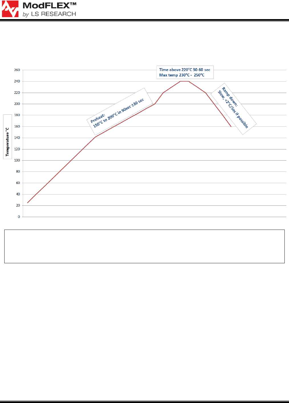
SOLDERING RECOMMENDATIONS
Recommended Reflow Profile for Lead Free Solder
Note: The quality of solder joints on the castellations (‘half vias’) where they contact the
host board should meet the appropriate IPC Specification. See IPC-A-610-D Acceptability
of Electronic Assemblies, section 8.2.4 Castellated Terminations.”

TiWi-SL MODULE
DATASHEET
The information in this document is subject to change without notice.
Confirm the data is current by downloading the latest revision from www.lsr.com.
330-0085-R0.4 Copyright © 2011 LS Research, LLC Page 27 of 36
CLEANING
In general, cleaning the populated modules is
strongly discouraged. Residuals under the
module cannot be easily removed with any
cleaning process.
• Cleaning with water can lead to capillary
effects where water is absorbed into the gap
between the host board and the module.
The combination of soldering flux residuals
and encapsulated water could lead to short
circuits between neighboring pads. Water
could also damage any stickers or labels.
• Cleaning with alcohol or a similar organic
solvent will likely flood soldering flux
residuals into the RF shield, which is not
accessible for post-washing inspection. The
solvent could also damage any stickers or
labels.
• Ultrasonic cleaning could damage the
module permanently.
OPTICAL INSPECTION
After soldering the Module to the host board,
consider optical inspection to check the
following:
• Proper alignment and centering of the
module over the pads.
• Proper solder joints on all pads.
• Excessive solder or contacts to neighboring
pads, or vias.
REWORK
The TiWi-SL module can be unsoldered from
the host board. Use of a hot air rework tool and
hot plate for pre-heating from underneath is
recommended. Avoid overheating.
Never attempt a rework on the
module itself, e.g. replacing
individual components. Such actions
will terminate warranty coverage.
SHIPPING, HANDLING, AND STORAGE
Shipping
Bulk orders of the TiWi-SL modules are
delivered in trays of 50.
Handling
The TiWi-SL modules contain a highly sensitive
electronic circuitry. Handling without proper
ESD protection may destroy or damage the
module permanently. ESD protection may
destroy or damage the module permanently.
Moisture Sensitivity Level (MSL)
MSL 4, per J-STD-020
Devices not stored in a sealed bag with
desiccant pack should be baked.
After opening devices that will be subjected to
reflow must be mounted within 72 hours of
factory conditions (<30°C and 60% RH) or
stored at <10% RH.
Bake devices for 8 hours at 125°C.
Storage
Storage/shelf life in sealed bags is 12 months at
<40°C and <90% relative humidity.
Repeating Reflow Soldering
Only a single reflow soldering
process is encouraged for host
boards.
TiWi-SL MODULE
DATASHEET
The information in this document is subject to change without notice.
Confirm the data is current by downloading the latest revision from www.lsr.com.
330-0085-R0.4 Copyright © 2011 LS Research, LLC Page 28 of 36
AGENCY CERTIFICATIONS
FCC ID: TFB-TIWISL01, 15.247.
IC ID: 5969A-TIWISL01, RSS 210
ETSI: The European Telecommunications Standards Institute. It produces the radio and
communication standards for Europe. Our testing is to the ETSI standards EN 300 328 and
EN 301 489, which are the portions of the relevant directives needed for a radio to obtain a CE mark.
AGENCY STATEMENTS
Federal Communication Commission Interference Statement
This equipment has been tested and found to comply with the limits for a Class B digital device,
pursuant to Part 15 of the FCC Rules. These limits are designed to provide reasonable protection
against harmful interference in a residential installation. This equipment generates uses and can radiate
radio frequency energy and, if not installed and used in accordance with the instructions, may cause
harmful interference to radio communications. However, there is no guarantee that interference will not
occur in a particular installation. If this equipment does cause harmful interference to radio or television
reception, which can be determined by turning the equipment off and on, the user is encouraged to try
to correct the interference by one of the following measures:
• Reorient or relocate the receiving antenna.
• Increase the separation between the equipment and receiver.
• Connect the equipment into an outlet on a circuit different from that to which the receiver is
connected.
• Consult the dealer or an experienced radio/TV technician for help.
This device complies with Part 15 of the FCC Rules. Operation is subject to the following two
conditions: (1) This device may not cause harmful interference, and (2) this device must accept any
interference received, including interference that may cause undesired operation.
FCC CAUTION: Any changes or modifications not expressly approved by the party
responsible for compliance could void the user's authority to operate this equipment.

TiWi-SL MODULE
DATASHEET
The information in this document is subject to change without notice.
Confirm the data is current by downloading the latest revision from www.lsr.com.
330-0085-R0.4 Copyright © 2011 LS Research, LLC Page 29 of 36
Industry Canada Statements
Operation is subject to the following two conditions: (1) this device may not cause interference, and (2)
this device must accept any interference, including interference that may cause undesired operation of
the device.
To reduce potential radio interference to other users, the antenna type and its gain should be so
chosen that the equivalent isotropically radiated power (e.i.r.p.) is not more than that permitted for
successful communication.
This device has been designed to operate with the antenna(s) listed below, and having a maximum
gain of 4.3 dBi (LSR Dipole) and 1.3dBi (Johanson Chip). Antennas not included in this list or having a
gain greater than 4.3 dBi and 1.3dBi are strictly prohibited for use with this device. The required
antenna impedance is 50 ohms.
List of all Antennas Acceptable for use with the Transmitter
1) LS Research 001-0001 center-fed dipole antenna and LS Research 080-0001 u.fl to Reverse Polarity
SMA connector cable.
2) Johanson 2450AT43B100 chip antenna.
L'opération est soumise aux deux conditions suivantes: (1) cet appareil ne peut pas provoquer
d'interférences et (2) cet appareil doit accepter toute interférence, y compris les interférences qui
peuvent causer un mauvais fonctionnement de l'appareil.
Pour réduire le risque d'interférence aux autres utilisateurs, le type d'antenne et son gain doiventêtre
choisis de manière que la puissance isotrope rayonnée équivalente (PIRE) ne dépasse pascelle
permise pour une communication réussie.
Cet appareil a été conçu pour fonctionner avec l'antenne (s) ci-dessous, et ayant un gain maximum de
4,3 dBi (LSR dipôle) et1.3dBi (Chip Johanson). Antennes pas inclus danscette liste ou d'avoir un gain
supérieur à 4,3 dBi et-1.3dBi sont strictement interdites pour l'utilisation avec cet appareil. L'impédance
d'antenne requise est de 50 ohms.
Liste de toutes les antennes acceptables pour une utilisation avec l'émetteur
1) LS Research 001-0001 alimenté par le centre antenne dipôle et LS Research 080-0001
U.FL d'inversion de polarité du câble connecteur SMA.
2) Antenne Johanson puce 2450AT43B100.

TiWi-SL MODULE
DATASHEET
The information in this document is subject to change without notice.
Confirm the data is current by downloading the latest revision from www.lsr.com.
330-0085-R0.4 Copyright © 2011 LS Research, LLC Page 30 of 36
OEM RESPONSIBILITIES TO COMPLY WITH FCC AND INDUSTRY CANADA
REGULATIONS
The TiWi-SL Module has been certified for integration into products only by OEM integrators under the
following conditions:
This device is granted for use in Mobile only configurations in which the antennas used for this
transmitter must be installed to provide a separation distance of at least 20cm from all person and not
be co-located with any other transmitters except in accordance with FCC and Industry Canada multi-
transmitter product procedures.
As long as the two conditions above are met, further transmitter testing will not be required.
However, the OEM integrator is still responsible for testing their end-product for any additional
compliance requirements required with this module installed (for example, digital device
emissions, PC peripheral requirements, etc.).
IMPORTANT NOTE: In the event that these conditions cannot be met (for certain
configurations or co-location with another transmitter), then the FCC and Industry
Canada authorizations are no longer considered valid and the FCC ID and IC Certification
Number cannot be used on the final product. In these circumstances, the OEM integrator
will be responsible for re-evaluating the end product (including the transmitter) and
obtaining a separate FCC and Industry Canada authorization.
Le module de TiWi-SL a été certifié pour l'intégration dans des produits uniquement par des
intégrateurs OEM dans les conditions suivantes:
Ce dispositif est accordé pour une utilisation dans des configurations mobiles seul dans lequel les
antennes utilisées pour cet émetteur doit être installé pour fournir une distance de séparation d'au
moins 20cm de toute personne et ne pas être colocalisés avec les autres émetteurs, sauf en conformité
avec la FCC et de l'Industrie Canada, multi-émetteur procédures produit.
Tant que les deux conditions précitées sont réunies, les tests de transmetteurs supplémentaires ne
seront pas tenus. Toutefois, l'intégrateur OEM est toujours responsable de tester leur produit final pour
toutes les exigences de conformité supplémentaires requis avec ce module installé (par exemple, les
émissions appareil numérique, les exigences de périphériques PC, etc.)
NOTE IMPORTANTE: Dans le cas où ces conditions ne peuvent être satisfaites (pour
certaines configurations ou de co-implantation avec un autre émetteur), puis la FCC et
Industrie autorisations Canada ne sont plus considérés comme valides et l'ID de la FCC
et IC numéro de certification ne peut pas être utilisé sur la produit final. Dans ces
circonstances, l'intégrateur OEM sera chargé de réévaluer le produit final (y compris
l'émetteur) et l'obtention d'un distincte de la FCC et Industrie Canada l'autorisation.

TiWi-SL MODULE
DATASHEET
The information in this document is subject to change without notice.
Confirm the data is current by downloading the latest revision from www.lsr.com.
330-0085-R0.4 Copyright © 2011 LS Research, LLC Page 31 of 36
OEM LABELING REQUIREMENTS FOR END-PRODUCT
The TiWi-SL Module is labeled with its own FCC ID and IC Certification Number. The FCC ID and IC
certification numbers are not visible when the module is installed inside another device, as such the
end device into which the module is installed must display a label referring to the enclosed module.
The final end product must be labeled in a visible area with the following:
“Contains Transmitter Module FCC ID: TFB-TIWISL01”
“Contains Transmitter Module IC: 5969A-TIWISL01”
or
“Contains FCC ID: TFB- TIWISL01”
“Contains IC: 5969A-TIWISL01”
The OEM of the TiWi-SL Module must only use the approved antenna(s) listed above, which have been
certified with this module.
Le module de TiWi-SL est étiqueté avec son propre ID de la FCC et IC numéro de certification. L'ID de
la FCC et IC numéros de certification ne sont pas visibles lorsque le module est installé à
l'intérieur d'un autre appareil, comme par exemple le terminal dans lequel le module est installé
doit afficher une etiquette faisant référence au module ci-joint. Le produit final doit être étiqueté dans un
endroit visible par le suivant:
“Contient Module émetteur FCC ID: TFB-TIWISL01"
“Contient Module émetteur IC: 5969A-TIWISL01"
ou
“Contient FCC ID: TFB-TIWISL01"
“Contient IC: 5969A-TIWISL01"
Les OEM du module TiWi-SL ne doit utiliser l'antenne approuvée (s) ci-dessus, qui ont été
certifiés avec ce module.

TiWi-SL MODULE
DATASHEET
The information in this document is subject to change without notice.
Confirm the data is current by downloading the latest revision from www.lsr.com.
330-0085-R0.4 Copyright © 2011 LS Research, LLC Page 32 of 36
OEM END PRODUCT USER MANUAL STATEMENTS
The OEM integrator should not to provide information to the end user regarding how to install or
remove this RF module or change RF related parameters in the user manual of the end product.
The user manual for the end product must include the following information in a prominent
location:
This device is granted for use in Mobile only configurations in which the antennas used for this
transmitter must be installed to provide a separation distance of at least 20cm from all person and not
be co-located with any other transmitters except in accordance with FCC and Industry Canada multi-
transmitter product procedures.
Other user manual statements may apply.
L'intégrateur OEM ne devraient pas fournir des informations à l'utilisateur final sur la façon d'installer ou
de supprimer ce module RF ou modifier les paramètres liés RF dans le manuel utilisateur du produit
final.
Le manuel d'utilisation pour le produit final doit comporter les informations suivantes dans
unendroit bien en vue:
Ce dispositif est accordé pour une utilisation dans des configurations mobiles seule dans laquelle les
antennes utilisées pour cet émetteur doit être installé pour fournir une distance de séparation d'au
moins 20cm de toute personne et ne pas être co-localisés avec les autres émetteurs, sauf en
conformité avec FCC et Industrie Canada, multi-émetteur procédures produit.
Autres déclarations manuel de l'utilisateur peuvent s'appliquer.
TiWi-SL MODULE
DATASHEET
The information in this document is subject to change without notice.
Confirm the data is current by downloading the latest revision from www.lsr.com.
330-0085-R0.4 Copyright © 2011 LS Research, LLC Page 33 of 36
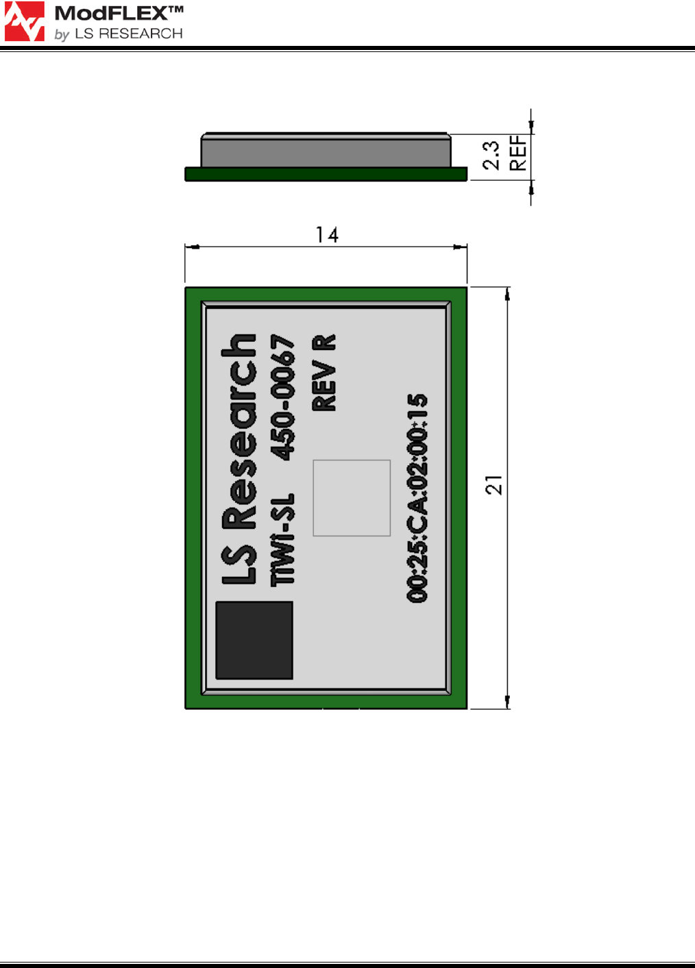
MECHANICAL DATA
Figure 4: Module Mechanical Dimensions (Maximum Module Height = 2.4 mm)
TiWi-SL MODULE
DATASHEET
The information in this document is subject to change without notice.
Confirm the data is current by downloading the latest revision from www.lsr.com.
330-0085-R0.4 Copyright © 2011 LS Research, LLC Page 34 of 36
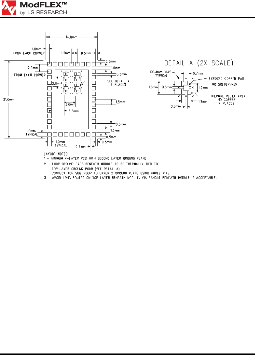
Figure 5: TiWi-SL Footprint.
TiWi-SL MODULE
DATASHEET
The information in this document is subject to change without notice.
Confirm the data is current by downloading the latest revision from www.lsr.com.
330-0085-R0.4 Copyright © 2011 LS Research, LLC Page 35 of 36
DEVICE MARKINGS
Rev 1 Devices
CC3000 Silicon Rev Front End
CC3000BYFVR TQM679002A
Where R = major revision
TiWi-SL MODULE
DATASHEET
The information in this document is subject to change without notice.
Confirm the data is current by downloading the latest revision from www.lsr.com.
330-0085-R0.4 Copyright © 2011 LS Research, LLC Page 36 of 36
CONTACTING LS RESEARCH
Headquarters LS Research, LLC
W66 N220 Commerce Court
Cedarburg, WI 53012-2636
USA
Tel: (262) 375-4400
Fax: (262) 375-4248
Website http://www.lsr.com
Technical Support http://forum.lsr.com
Wiki http://wiki.lsr.com/TiWi.ashx
Sales Contact sales@lsr.com
The information in this document is provided in connection with LS Research (hereafter referred to as “LSR”)
products. No license, express or implied, by estoppel or otherwise, to any intellectual property right is granted by
this document or in connection with the sale of LSR products. EXCEPT AS SET FORTH IN LSR’S TERMS AND
CONDITIONS OF SALE LOCATED ON LSR’S WEB SITE, LSR ASSUMES NO LIABILITY WHATSOEVER AND
DISCLAIMS ANY EXPRESS, IMPLIED OR STATUTORY WARRANTY RELATING TO ITS PRODUCTS
INCLUDING, BUT NOT LIMITED TO, THE IMPLIED WARRANTY OF MERCHANTABILITY, FITNESS FOR A
PARTICULAR PURPOSE, OR NON-INFRINGEMENT. IN NO EVENT SHALL LSR BE LIABLE FOR ANY
DIRECT, INDIRECT, CONSEQUENTIAL, PUNITIVE, SPECIAL OR INCIDENTAL DAMAGES (INCLUDING,
WITHOUT LIMITATION, DAMAGES FOR LOSS OF PROFITS, BUSINESS INTERRUPTION, OR LOSS OF
INFORMATION) ARISING OUT OF THE USE OR INABILITY TO USE THIS DOCUMENT, EVEN IF LSR HAS
BEEN ADVISED OF THE POSSIBILITY OF SUCH DAMAGES. LSR makes no representations or warranties with
respect to the accuracy or completeness of the contents of this document and reserves the right to make changes
to specifications and product descriptions at any time without notice. LSR does not make any commitment to
update the information contained herein. Unless specifically provided otherwise, LSR products are not suitable
for, and shall not be used in, automotive applications. LSR’s products are not intended, authorized, or warranted
for use as components in applications intended to support or sustain life.