Landis Gyr Technology NG0R1S3 Series 5 Single Board Radio User Manual 15 0460 Exhibit Cover
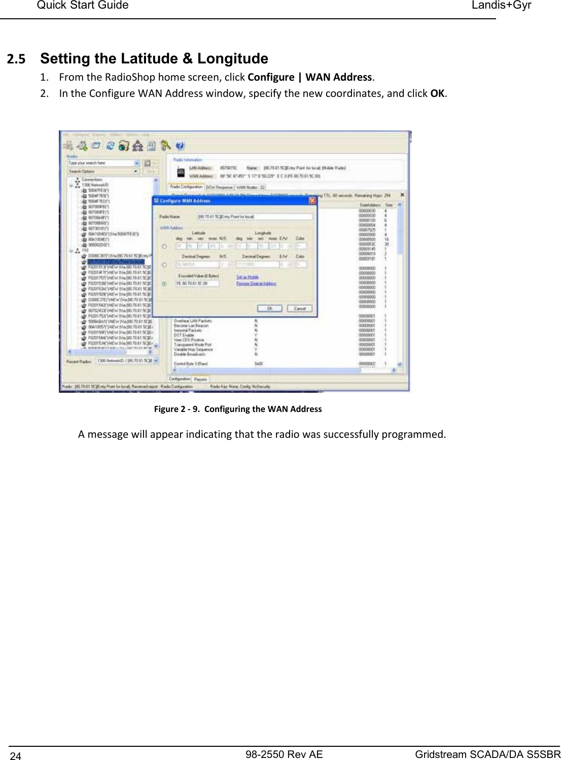
Landis+Gyr Technology, Inc. Series 5 Single Board Radio 15 0460 Exhibit Cover
UserManual.wiki
>
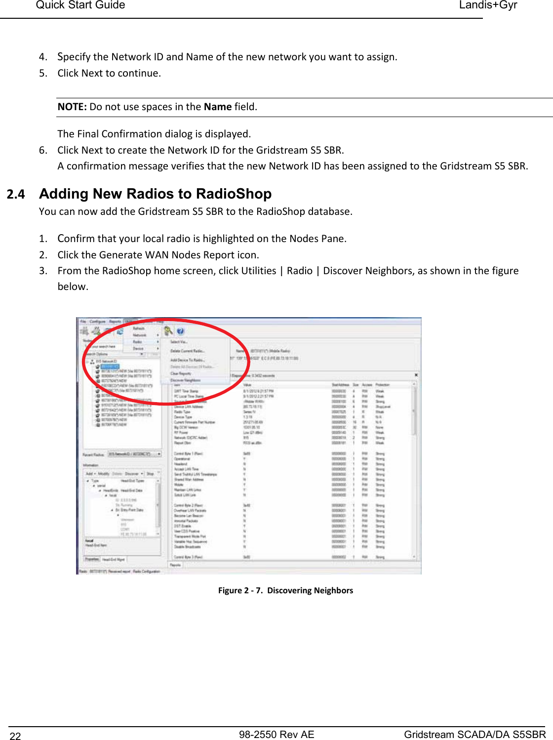
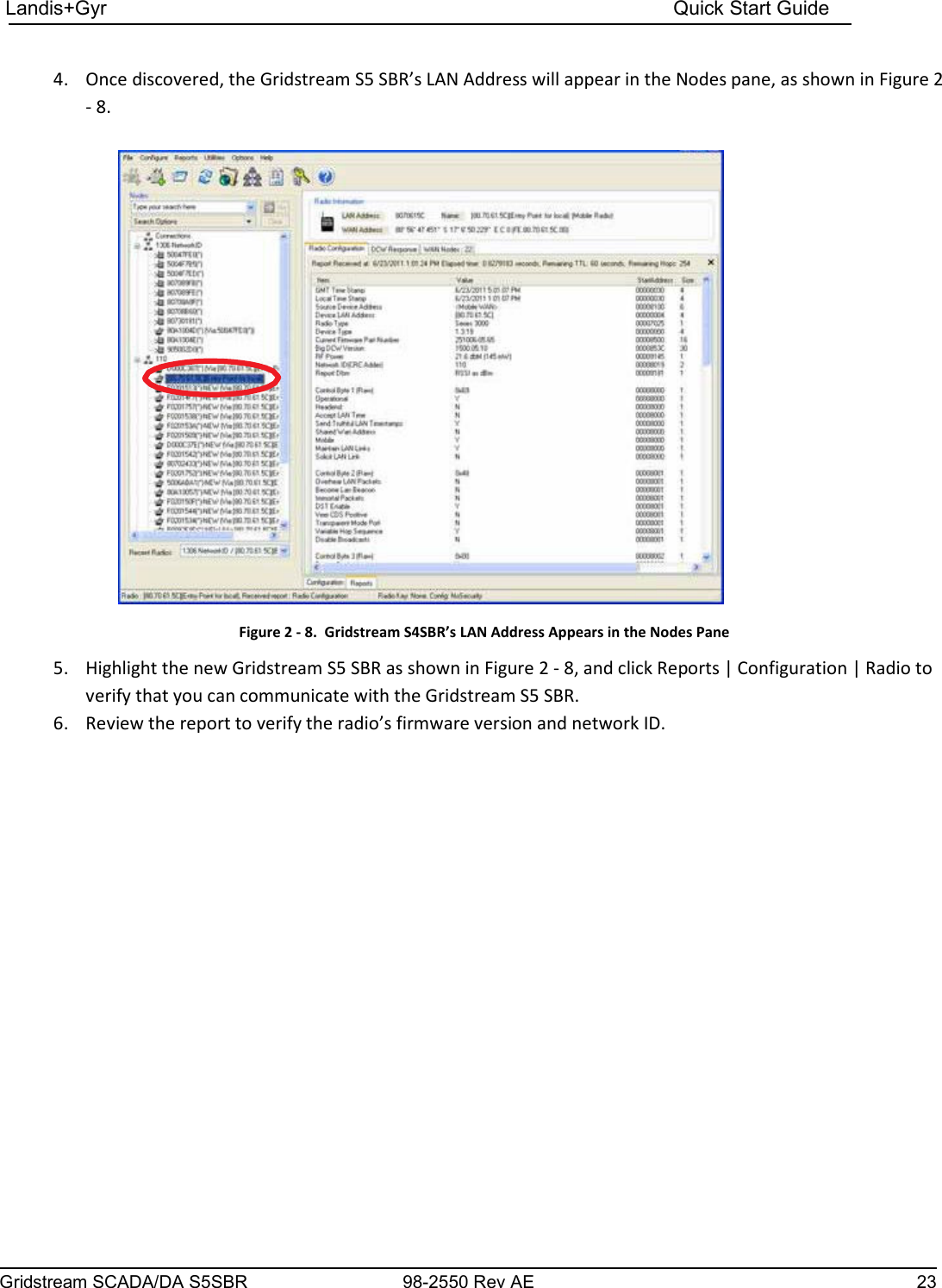
Landis Gyr Technology
>
NG0R1S3 User Manual
>
Manual
Contents
1.
Manual
2.
User Manual
Manual
Navigation menu
Upload a User Manual
Namespaces
Wiki Guide
HTML
PDF
Info
Views
User Manual
Discussion / Help
Navigation

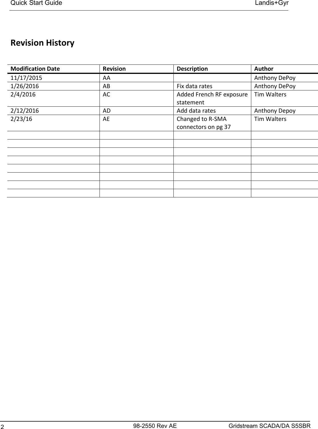
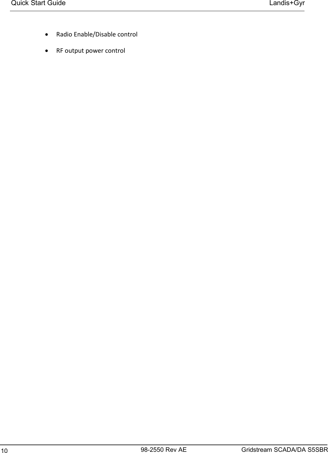
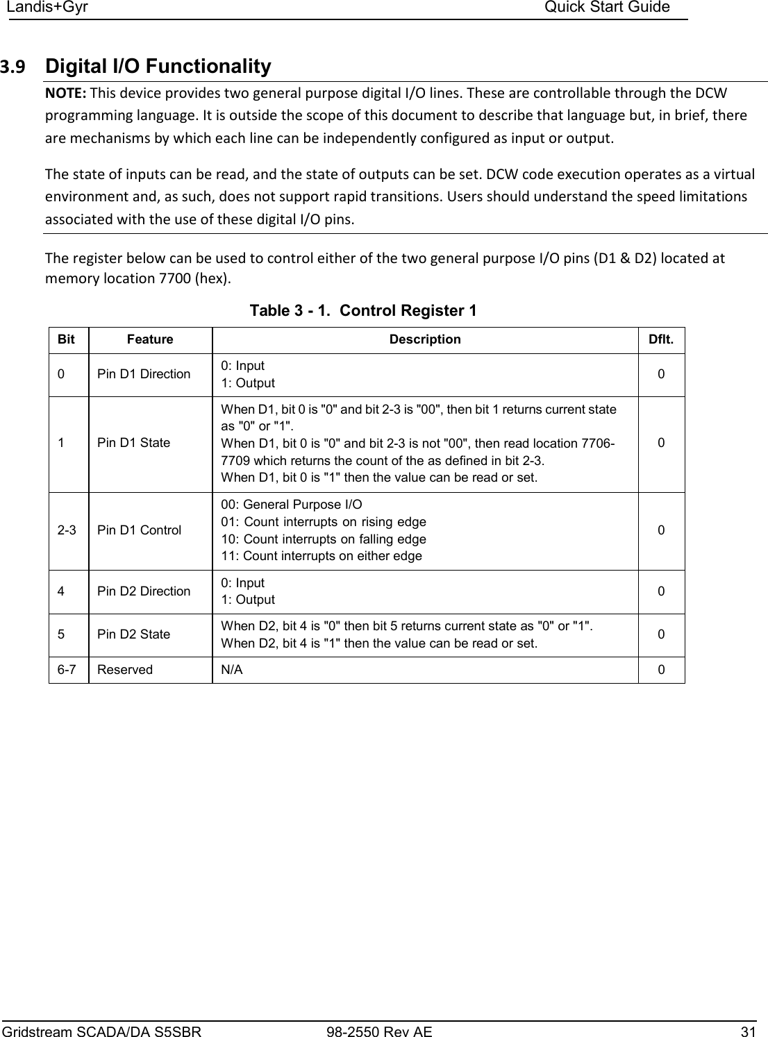
![Gridstream SCADA/DA S5SBR 98-2550 Rev AE 11 Landis+Gyr Quick Start Guide 1.3 Pin Functions Pin Outs for the connector as described below are designed to interface with developer OEM architecture. Figure 1 - 4. Pinout Diagram (Rear View) For All Board Versions) Table 1 - 4. I/O Connector Pin Functions and Acceptable Voltage Levels Pin Number Name Function Logic Level Low Logic Level High (VDC) J1-1,2,3,4,6 VIN Main supply for the board. 0 4.0 ~ 7.0 Nominal = 5.0 J1- 27 LPP TX This pin is an output from the device for connecting to RadioShop via the LAN Packet Port (LPP) interface. 0 ~ 0.5 3.1 ~ 3.6 J1- 25 LPP RX This pin is an input to the device for connecting to RadioShop via the LAN Packet Port (LPP) interface. 0 ~ 0.5 3.1 ~ 3.6 J1- 37 DIGITAL_IO1 A general purpose Digital Input / Output Pin. The application- specific DCW can use this pin as desired. 0 ~ 0.5 3.1 ~ 3.6 J1- 45 ANALOG_IO1 An input to the device’s A/D converter. The application- specific DCW can read the voltage on this pin. Note: This pin may be configured as a Digital I/O, if desired. 0 ~ 2.5 J1- 7,8,9,10, 11,12 GND Common ground for both power and communications. These two pins are tied together on the device. 0 0 J1- 15 LOW_RF_POWER Digital input used to select Low-Power Mode, an RF output power reduction to 150 mW [22 dBm]. ground 3.6V max J1- 29 Outage detect Digital input used to completely shut down the device. ground 3.1 ~ 3.6V max J1- 47 ANALOG_IO2 An input to the device’s A/D converter. The application- specific DCW can read the voltage on this pin. Note: This pin may be configured as a Digital I/O, if desired. 0 ~ 2.5 J1- 39 DIGITAL_IO2 A general purpose Digital Input / Output Pin. The application- specific DCW can use this pin as desired. 0 ~ 0.6 3.16 ~ 3.6 J1- 48 TXD_COMM This pin is an input to the Transparent Port (TPP) device. 0 ~ 0.6 2.6 ~ 3.4 J1- 48 RXD_COMM This pin is an output from the Transparent Port (TPP) device. 0 ~ 0.5 2.8 ~ 3.4](https://usermanual.wiki/Landis-Gyr-Technology/NG0R1S3.Manual/User-Guide-2920118-Page-12.png)
![98-2550 Rev AE 12 Gridstream SCADA/DA S5SBR Quick Start Guide Landis+Gyr 1.4 Pin J1-1, 2, 3, 4, 6 (VIN) This pin must be supplied with DC voltage between 4.0 and 7.0 VDC with 5.0 VDC considered nominal. The input voltage is linearly regulated on the board. While the linear regulation can remove some noise, Power Supply Rejection Ratio (PSRR) varies with frequency. If the power source is particularly noisy, filtering may be required. Landis+Gyr engineering can assist in defining radio tests to determine if power supply noise is affecting radio performance. The input voltage must be maintained between 4.0 VDC and 7.0 VDC during operation. The on- board electronics include fast-acting reset circuitry. If the voltage drops below 4.0 VDC, even transiently, the system will reboot once the voltage returns to normal range. If the voltage rises above 7.1 VDC, even transiently, the voltage-sensitive components could be damaged. Upon power up, the on-board processor and voltage regulator requires the supply voltage to have a minimum of 0.05 V/msec slew rate - which implies rising from a logic 0 to a logic 1 in no less than 66 msec. Power consumption during normal receive mode is typically 70 mA. Current consumption during 50 mW transmit mode is 200 mA, 300 mA during 150 mW transmit mode, and 700 mA during 630 mW transmit mode. 1.5 Pin J1- 27 (LPP TX) and Pin J1-25 (LPP RX) These pins are used to interface with the device's LAN Packet Port. These pins are driven at TTL level supply, 3.6 VDC. Baud rates on this port default to 9,600 bps but, using RadioShop, are configurable from 1,200 bps to 115,200 bps. To reduce chances of electrical damage, a 10Kohm series resistor is placed in-series with the pin which limits the drive current capability of this pin. Stray physical capacitance on this circuit should be kept below 250[pF]. NOTE: These pins should NOT be directly connected to an RS-232 interface on a computer. Where such a connection is necessary, the developer must connect to the unit through an externally- powered TTL to RS-232 VDC converter, NOT via the pins or the RS-232 connection on the computer.](https://usermanual.wiki/Landis-Gyr-Technology/NG0R1S3.Manual/User-Guide-2920118-Page-13.png)
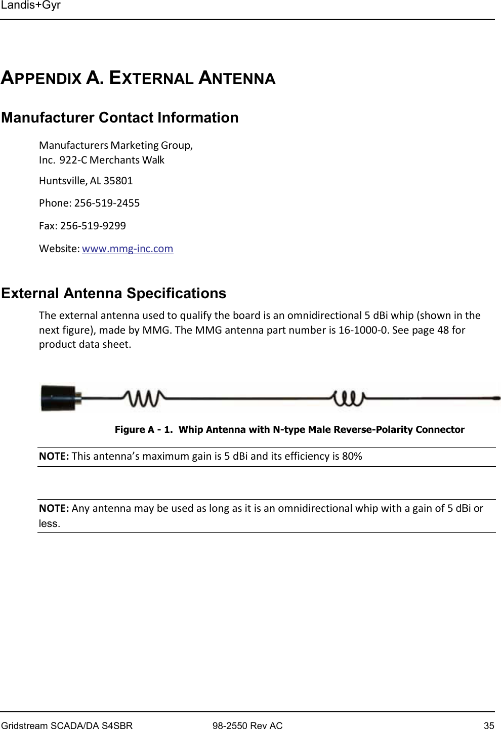
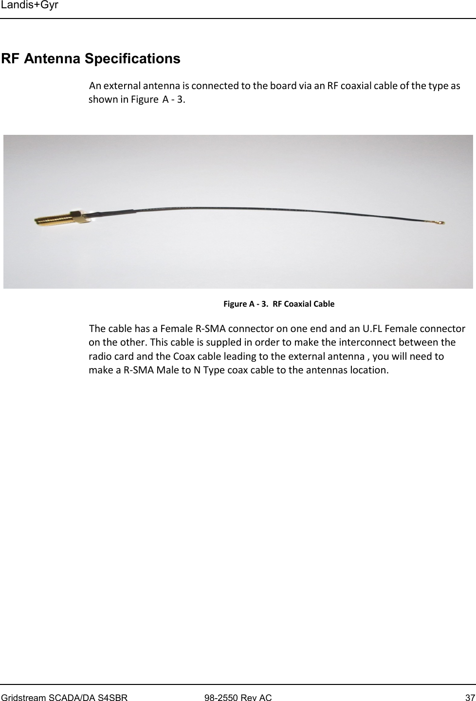
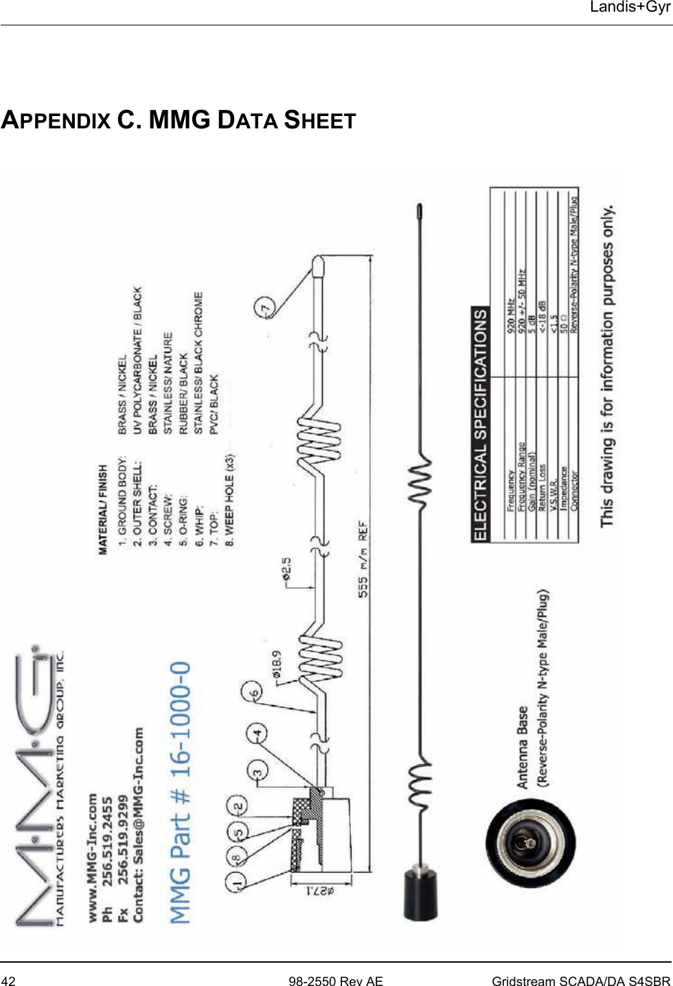
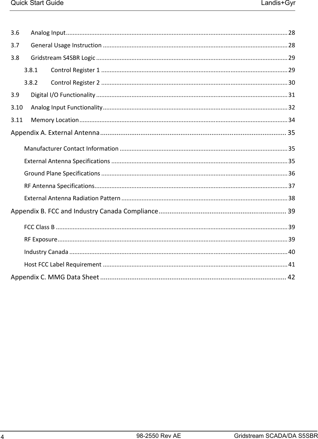
![98-2550 Rev AE 16 Gridstream SCADA/DA S5SBR Quick Start Guide Landis+Gyr 1.11 Pin 12 (TPP RX) and Pin 13 (TPP TX) These pins are used to interface with the device's Transparent Port. These pins are driven at TTL supply level. Baud rates on this port default to 9,600 bps but, using RadioShop, are configurable to 115.2Kbps. To reduce chances of electrical damage, a 1Kohm series resistor is placed in-series with the pin which limits the drive current capability of this pin. Stray physical capacitance on this circuit should be kept below 250[pF]. NOTE: These pins should NOT be directly connected to an RS-232 interface on a computer. Where such a connection is necessary, the developer must purchase a TTL to RS-32 VDC converter which is powered external and NOT via the pins or the RS-232 connection on the computer. 1.12 Antennas As with any RF device, antenna-related decisions are critical and must be made early. The RF range of the final product will depend greatly on the choice of antenna and where it is placed. 50-ohm U.FL connector to SMA female cable, for RF co-axes connection to an external antenna. 1.13 External Antenna An external antenna is connected to the board via an U.FL coaxial SMA female RF cable. This cable is provided in order to mate to a Coax cable made to specification to fit location of antenna. See Figure A - 3. RF Coaxial Cable The external antenna used to qualify the board is an omnidirectional 5 dBi whip (shown in the next figure), made by Manufacturers Marketing Group (MMG). The MMG part number for this antenna is 16-1000-0. MMG contact information is on page 35. This antenna can be used, or any other omnidirectional whip antenna with 5 dBi gain or less. Figure 1 - 7. Whip Antenna with N-type Male Reverse-Polarity Connector NOTE: See “External Antenna Specifications’ on page for antenna technical specifications.](https://usermanual.wiki/Landis-Gyr-Technology/NG0R1S3.Manual/User-Guide-2920118-Page-17.png)
![Gridstream SCADA/DA S5SBR 98-2550 Rev AE 17 Landis+Gyr Quick Start Guide 1.14 Additional Specifications Table 1 - 7. Additional Specifications Category Specification Value(s) or Range(s) Networking Number of Channels 239 (narrow channel mode), 86 (wide channel mode) 51 UW, SUN 129 and 64 Channel Spacing 100 KHz (narrow channel mode), 300 KHz (wide channel mode) 200K and 400K SUN Modulation Type 2-FSK RF Baud Rate 9.6, 19.2, 38.4, 115.2, 300 kbps. SUN 50,150 and 200kbps FCC Operation Certification Part 15.247 Spreading Technique Frequency Hopping Hopping Technique Pseudo Random Asynchronous Hopping Patterns 65,536 (Unique per network) Network Address Latitude / Longitude Coordinates Turn-Around Time 100[uS] max Programming Programming Language Device Control Word (DCW) Radio Firmware Version 5.72 later Data LAN Packet Port (LPP) Serial Interface, DCW adjustable per specs below Data Rate - 9.6, 19.2, 38.4, 115.2 kbps Transparent Port (TPP) Serial Interface, DCW adjustable per specs below Data Rate - 9.6, 19.2, 38.4, 115.2 kbps Serial Interface TTL Parity Odd, Even, or None Data bits 7 or 8 Stop bits 1 or 2 Duplex Full Protocol Any asynchronous byte-oriented protocol Environmental Operating Temperature -40°C to +85°C Storage Temperature -40°C to +85°C Humidity 85C, 85% RH Mechanical Size 1.5x1.5](https://usermanual.wiki/Landis-Gyr-Technology/NG0R1S3.Manual/User-Guide-2920118-Page-18.png)
![Landis+Gyr 32 98-2550 Rev AE Gridstream SCADA/DA S4SBR 3.10 Analog Input Functionality This device provides two general purpose analog inputs. These are filtered and connected to a 10-bit A/D converter. NOTE: The voltage reference for this A/D converter is 2.5 VDC +/- 60[mVDC] across the operating temperature range. This A/D converter has the following specifications: Table 3 - 2. A/D Converter Specifications A/D characteristic Specification Resolution 10 bit INL +/-5 LSB Absolute Accuracy +/-5 LSB DNL +/-1 LSB Offset Error +/-3 LSB Gain Error +/-3 LSB NOTE: The actual sampling time is 0.25 μS and the conversion time is 2.75 μS, but the rate at which signals on these inputs can be sampled in-practice is limited by the DCW execution. It is recommended that these channels be used only for DC voltage measurement, and that the sampling rate cannot exceed 100 mS.](https://usermanual.wiki/Landis-Gyr-Technology/NG0R1S3.Manual/User-Guide-2920118-Page-33.png)
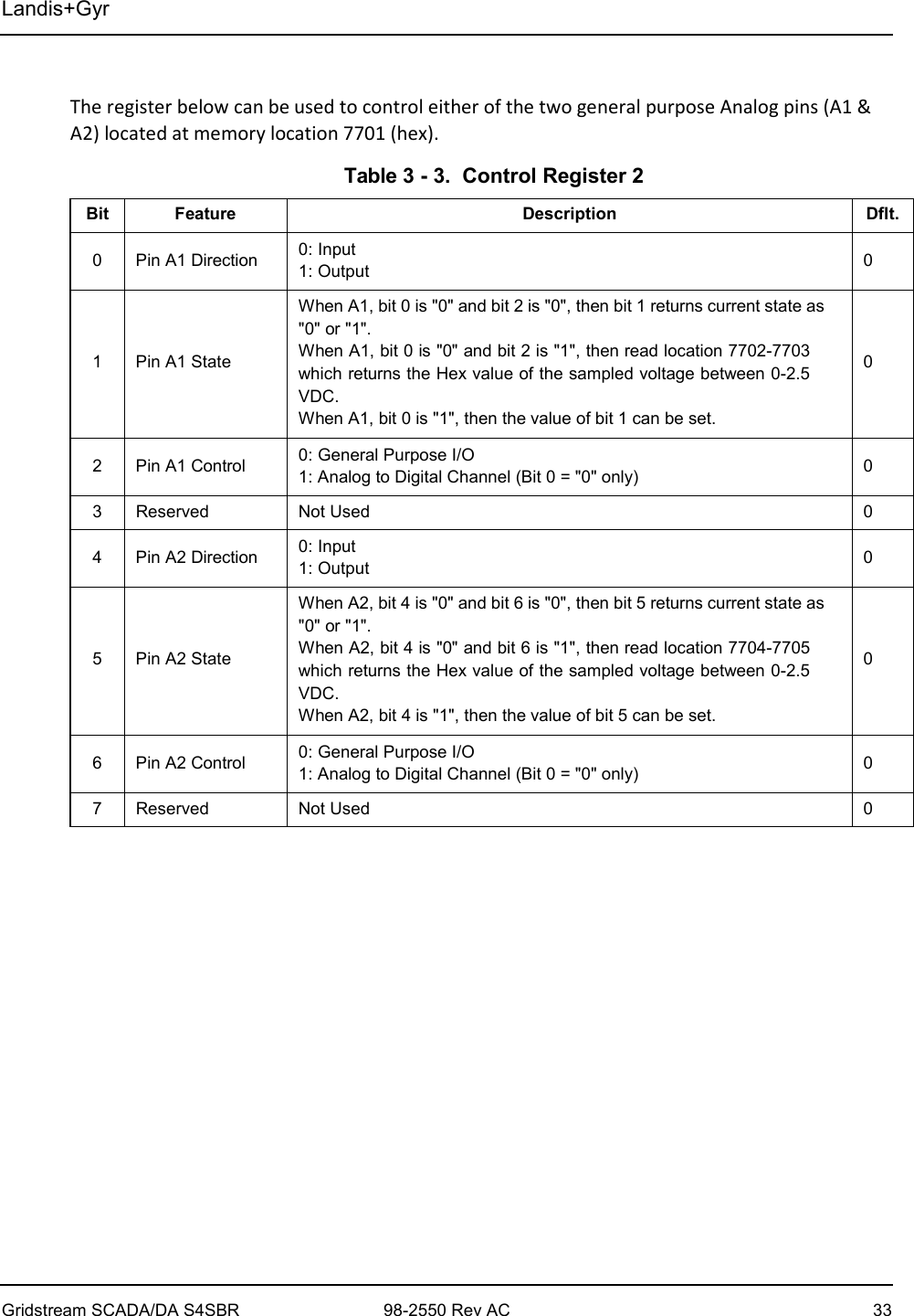
![Landis+Gyr 34 98-2550 Rev AE Gridstream SCADA/DA S4SBR 3.11 Memory Location Memory locations in the S4SBR [listed above in Table 3-3 and below as 77XX-77XXx] store commands to control (as outputs) and monitor the status (as inputs) of connected devices. [7702-7703h] Analog to Digital Channel A1. When A1 is set to “Analog to Digital” (Bit 2) this location will contain a 10-bit reading. The scale on this board is from 0 to 2.5 volts. Voltages greater than 2.5 VDC will be reported as 2.5 VDC. [7704-7705h] Analog to Digital Channel A2. When A2 is set to “Analog to Digital” (Bit 6) this location will contain a 10-bit reading. The scale on this board is from 0 to 2.5 volts. Voltages greater than 2.5 VDC will be reported as 2.5 VDC. [7706-7709h] D1 Interrupt Counter. If D1 is configured as an interrupt (Bit 2-3) then this location will count the number of interrupts that have been detected. NOTE: The interrupt counter is cleared each time interrupts are enabled.](https://usermanual.wiki/Landis-Gyr-Technology/NG0R1S3.Manual/User-Guide-2920118-Page-35.png)