Landis Gyr Technology NG0R1S3 Series 5 Single Board Radio User Manual 15 0460 Exhibit Cover
Landis+Gyr Technology, Inc. Series 5 Single Board Radio 15 0460 Exhibit Cover
Contents
- 1. Manual
- 2. User Manual
Manual

5015 B.U. Bowman Drive Buford, GA 30518 USA Voice: 770-831-8048 Fax: 770-831-8598
Certification Exhibit
FCC ID: R7PNG0R1S3
IC: 5294A-NG0R1S3
FCC Rule Part: 15.247
IC Radio Standards Specification: RSS-247
ACS Project Number: 15-0460
Manufacturer: Landis+Gyr Technology, Inc.
Model: S5 SBR
Manual
G
RIDSTREAM
M
ODULAR
SCADA/DA
S
ERIES
5
S
INGLE
B
OARD
R
ADIO
Q
UICK
S
TART
G
UIDE
Publication: 98-2550 Rev AE
Confidential & Proprietary
By accepting this document, each recipient agrees never to distribute this to others in whole or in part without the
prior written consent of Landis+Gyr. Unauthorized copies are prohibited by law. Landis+Gyr, Copyright © 2015

98-2550 Rev AE
2 Gridstream SCADA/DA S5SBR
Quick Start Guide Landis+Gyr
Revision History
Modification
Date
Revision
Description
Author
11/17/2015
AA
Anthony DePoy
1/26/2016
AB
Fix data rates
Anthony De
Poy
2/4/2016
AC
Added French RF exposure
statement
Tim Walters
2/12/2016
AD
Add data rates
Anthony Depoy
2/23/16
AE
Changed to R
-
SMA
connectors on pg 37
Tim Walters

Gridstream SCADA/DA S5SBR
98-2550 Rev AE 3
Landis+Gyr Quick Start Guide
Table of Contents
1 Introduction ............................................................................................................................. 5
1.1 Performance Specifications .............................................................................................................. 6
1.2 Electrical Interface ............................................................................................................................ 9
1.3 Pin Functions ................................................................................................................................... 11
1.4 Pin J1-1, 2, 3, 4, 6 (VIN) ................................................................................................................... 12
1.5 Pin J1- 27 (LPP TX) and Pin J1-25 (LPP RX) ...................................................................................... 12
1.6 Pin J1- 37 (DIGITAL_IO1) and Pin 39 (DIGITAL_IO2) ....................................................................... 13
1.7 Pin J1-45 (ANALOG_IO1) and Pin 47 (ANALOG_IO2) ...................................................................... 13
1.8 PinsJ1-7,8,9,10,11,12 (GND) ........................................................................................................... 14
1.9 Pin J1-15 (LOW_RF_POWER) .......................................................................................................... 15
1.10 Pin J1- 29 (Outage Detect) .............................................................................................................. 15
1.11 Pin 12 (TPP RX) and Pin 13 (TPP TX) ................................................................................................ 16
1.12 Antennas ......................................................................................................................................... 16
1.13 External Antenna ............................................................................................................................ 16
1.14 Additional Specifications ................................................................................................................. 17
2 Configuring and Testing ......................................................................................................... 18
2.1 Connecting to a Gridstream S5SBR Using RadioShop ..................................................................... 18
2.2 Assign the Network ID (CRC) of the Gridstream S5 SBR ................................................................. 19
2.3 Assigning a New Network ID to a Gridstream S5 SBR ..................................................................... 21
2.4 Adding New Radios to RadioShop ................................................................................................... 22
2.5 Setting the Latitude & Longitude .................................................................................................... 24
2.6 Troubleshooting .............................................................................................................................. 25
3 Development Environment ................................................................................................... 26
3.1 Gridstream SCADA/DA Series 5 Single Board Radio Interface Board ............................................. 26
3.2 Transparent Port (TPP) Connection ................................................................................................ 27
3.3 LAN Packet Port (LPP) Connection .................................................................................................. 27
3.4 Onboard Regulator ......................................................................................................................... 27
3.5 Digital Input ..................................................................................................................................... 28

98-2550 Rev AE
4 Gridstream SCADA/DA S5SBR
Quick Start Guide Landis+Gyr
3.6 Analog Input .................................................................................................................................... 28
3.7 General Usage Instruction .............................................................................................................. 28
3.8 Gridstream S4SBR Logic .................................................................................................................. 29
3.8.1 Control Register 1 ............................................................................................................... 29
3.8.2 Control Register 2 ............................................................................................................... 30
3.9 Digital I/O Functionality .................................................................................................................. 31
3.10 Analog Input Functionality .............................................................................................................. 32
3.11 Memory Location ............................................................................................................................ 34
Appendix A. External Antenna ...................................................................................................... 35
Manufacturer Contact Information .................................................................................................... 35
External Antenna Specifications ......................................................................................................... 35
Ground Plane Specifications ............................................................................................................... 36
RF Antenna Specifications ................................................................................................................... 37
External Antenna Radiation Pattern ................................................................................................... 38
Appendix B. FCC and Industry Canada Compliance ...................................................................... 39
FCC Class B .......................................................................................................................................... 39
RF Exposure ......................................................................................................................................... 39
Industry Canada .................................................................................................................................. 40
Host FCC Label Requirement .............................................................................................................. 41
Appendix C. MMG Data Sheet ...................................................................................................... 42
Gridstream SCADA/DA S5SBR
98-2550 Rev AE 5
Landis+Gyr Quick Start Guide
1 INTRODUCTION
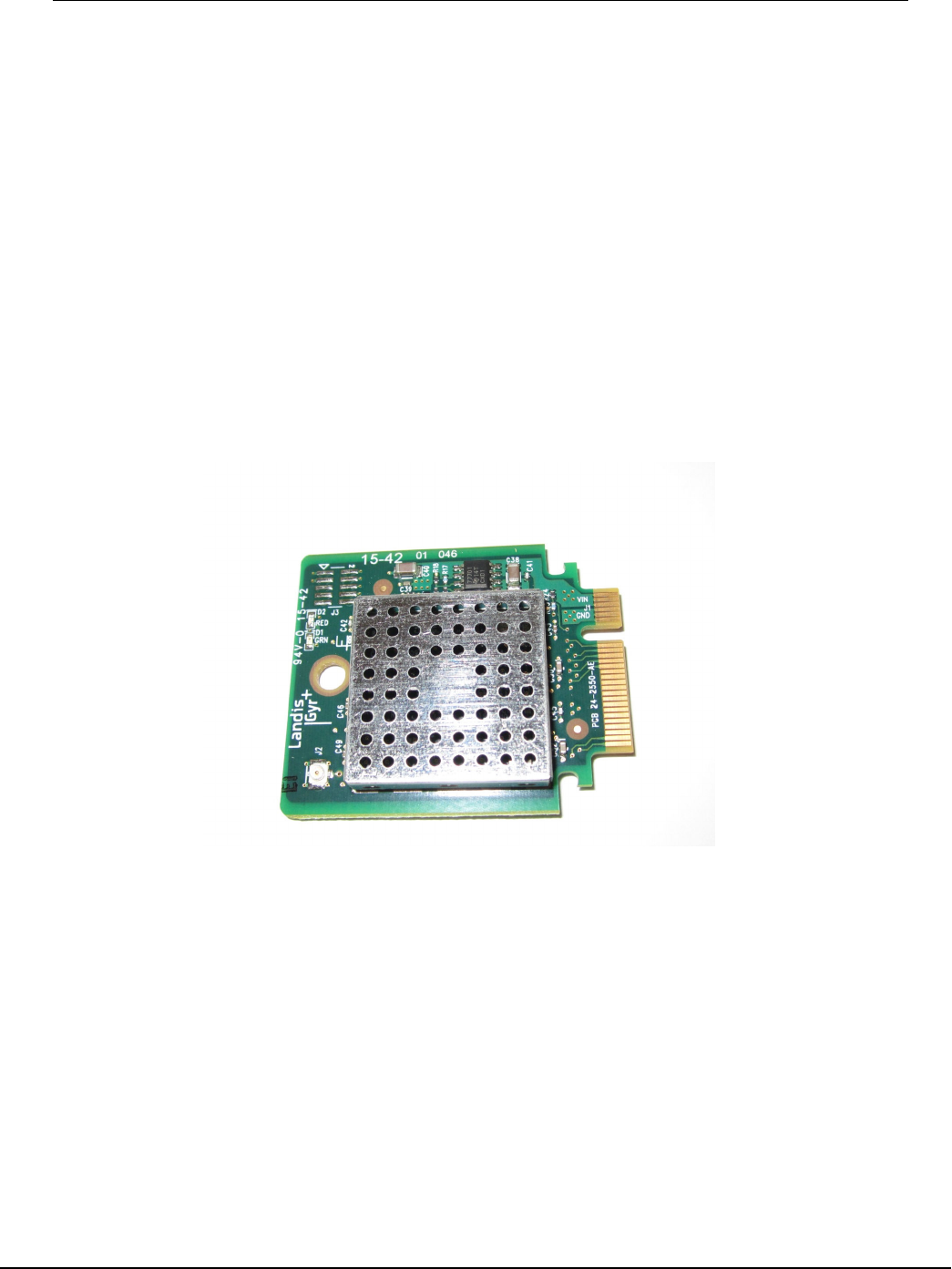
The Gridstream SCADA Series 5 Single Board Radio (Gridstream S5 SBR) is for use by OEM
vendors wanting to incorporate Gridstream capability into their SCADA/DA and similar products.
The design of the board allows integration with an OEM enclosure and communication with the
customer's equipment via a 50-pin connector. Table 1 - 4, "I/O Connector Pin Functions and
Acceptable Voltage Levels," provides details for the interface.
Figure 1-1. 40-2550 SBR S5 Radio card
The Gridstream S5 SBR is a self-contained 630 mW Integrated WanGate Radio (IWR) which
includes voltage regulation, micro-processor, and radio. Output power can be set to 50, 150, or
630mW.
Figure 1 - 2. Gridstream S5 SBR
This Gridstream S5SBR is based upon existing Gridstream architecture and will operate as a node
within a Gridstream network. It is similar in construction to a Gridstream metering endpoint, but
with an optional onboard antenna and I/O ports. It has received Modular FCC approval when
used with the approved cable and antenna.

98-2550 Rev AE
6 Gridstream SCADA/DA S5SBR
Quick Start Guide Landis+Gyr
The Gridstream S5 SBR provides two digital I/O ports and two analog input ports, which can also
be configured as two general purpose I/O ports. One of the digital ports can also be configured
as a counter by sensing either the rising end of the pulse, trailing edge of the pulse, or both.
These interfaces are accessible via the Device Control Word (DCW) programming language.
1.1 Performance Specifications
Table 1 - 1. Series 5 Gridstream S5 SBR General Electrical
Specifications
Parameter
Value
Units
Comments
Min Typ Max
Input Voltage 4.0 5.0 7.0 VDC
Current Consumption
Rx mode
Tx mode (low power)†
Tx mode (medium power)†
Tx mode (high power)†
70
200
250
600
250
330
750
mA
Current Consumption
Shut Down mode*
85
100
µA
V
in
= 5V
*PWR_DN = 0V
RF Frequency Range 902.2
927.8 MHz
RF Baud Rate
9.6
300
kbps Variable - 9.6, 19.2, 38.4,
115.2 kbps, ext
Frequency Stability -3
+3 ppm Over temperature range
Processor
Processor Type
Clock Speed
RAM (internal)
Flash (internal)
SAM 4 C
39
256
2
MHz
KB
MEG
Additional Memory
Flash
32
MBIT

Gridstream SCADA/DA S5SBR
98-2550 Rev AE 7
Landis+Gyr Quick Start Guide
Table 1 - 2. Series 5 Gridstream S5 SBR Transmitter Electrical
Specifications
Parameter
Value
Units
Comments
Min Typ Max
Modulation Type FSK/GFSK
Depends on baud rate
Baud Rates
9.6
kbps
± 4.95 kHz
19.2
38.4
± 9.9 kHz
± 19.8 kHz
115.2
50.00
300.00
150.00
200.00
± 57.6 kHz
Mod index 1
(Ultra-Wide) Mod index 0.5
(SUN Mode) Mod index 0.5
(SUN Mode) Mod index 0.5
Output Power
27
21
28
22
29
23
dBm
Over temperature range, <2:1
High Setting (6300 mW)‡
Medium Setting (150 mW)
VSWR load
Low Setting (50 mW) 16 17 18 ‡Default Factory Setting
Ruggedness +30dBm, 40% duty cycle, open
circuit on antenna port
No Damage
Conducted Spurious
Second harmonic
All other harmonics
-40
-70
dBc
At +30dBm output power,
<2:1 VSWR load
Meets FCC requirements

98-2550 Rev AE
8 Gridstream SCADA/DA S5SBR
Quick Start Guide Landis+Gyr
Table 1 - 3. Series 5 Gridstream S5SBR Receiver Electrical
Specifications
Parameter
Value
Units
Comments
Min Typ Max
Cascaded Noise Figure
5.0
dB
Input IP3
-10
dBm
Two-tone test (1 MHz tone
spacing); desired signal 3dB
above sensitivity; 9.6 kbps
operation
Sensitivity (@ 25° C)
-112
dBm
9.6 kbps
19.2 kbps -110
38.4 kbps -107
115.2 kbps -101
Image Rejection (worst-case)
30
dB
Desired signal 3dB above
sensitivity, CW jammer (at
image freq) increased until
PER = 10%; 9.6kbps baud
rate
Selectivity (In
-
ban
d blocking)
30
35
80
dB
Desired signal 3dB above
f
0
± 100 kHz
f
0
± 200 kHz
f
0
± 10 MHz
sensitivity,
CW jammer (at
image freq) increased until
PER = 10%; 9.6kbps baud
rate
Blocking (Out-of-band)
0
dBm
Desired signal 3dB above
No Pager-Reject Filter sensitivity, CW jammer (at
f < 880 MHz image freq) increased until
880 < f < 895 MHz -10 PER = 10%; 9.6kbps baud
960 < f < 3000 MHz -10 rate
Maximum input RF power
ISM Band
902.2 MHz < f < 927.8MHz
+10
dBm
Permanent damage can
occur to receiver if exposed
to RF level above this
specification
Minimum spacing between S5 SBR antenna
and any other device transmitting in the ISM
band
902.2 MHz < f < 927.8MHz
8
inches
Applies to both internal and
external antenna versions of
S5 SBR
Gridstream SCADA/DA S5SBR
98-2550 Rev AE 9
Landis+Gyr Quick Start Guide
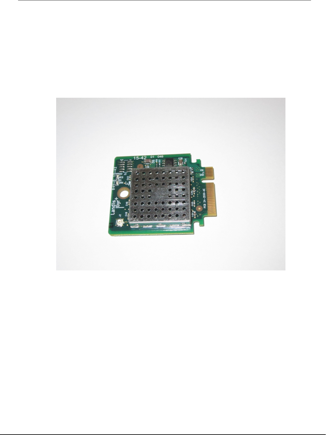
1.2 Electrical Interface
The electrical interface for power and control circuitry is provided via a 50-pin keyed connector
located on the side of the board and shown in figure below.
The Gridstream S5SBR requires a nominal 5.0 VDC supply, with a total input range of 4.0 to 7.0
VDC. Samtec right angle HSEC8 16-1720
Figure 1 - 3. Gridstream Series 5 Single Board Radio Rear View, I/O Connector, Pin 1 (Red Arrow)
The I/O connector provides seven interface connections listed below:
• Input power connections
• LAN Packet Port (LPP)
• Transparent Port (TPP)
• Digital I/O signals
• Analog I/O signals

98-2550 Rev AE
10
Gridstream SCADA/DA S5SBR
Quick Start Guide Landis+Gyr
• Radio Enable/Disable control
• RF output power control

Gridstream SCADA/DA S5SBR
98-2550 Rev AE 11
Landis+Gyr Quick Start Guide
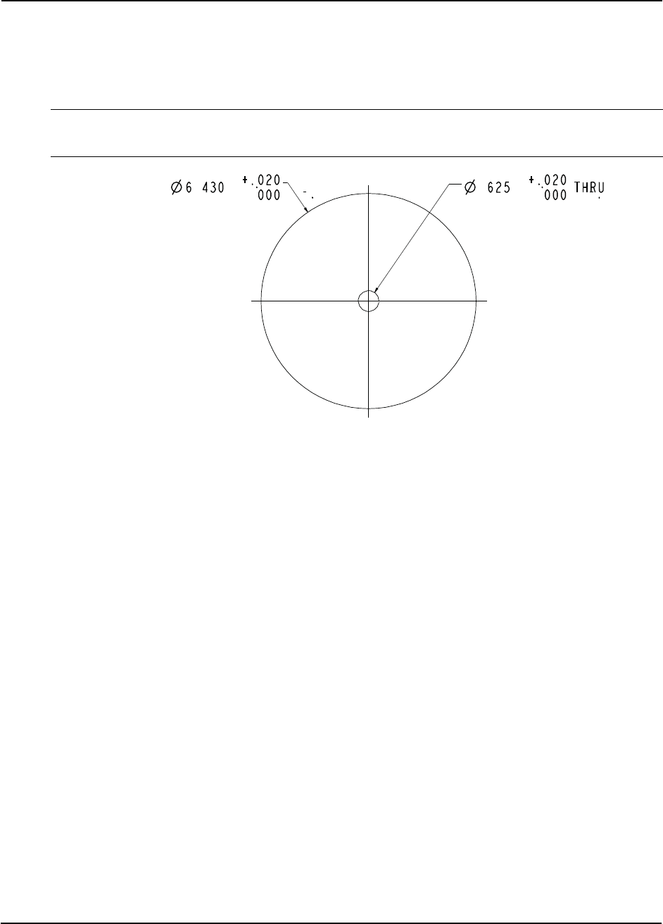
1.3 Pin Functions
Pin Outs for the connector as described below are designed to interface with developer OEM
architecture.
Figure 1 - 4. Pinout Diagram (Rear View) For All Board Versions)
Table 1 - 4. I/O Connector Pin Functions and Acceptable Voltage Levels
Pin
Number
Name
Function
Logic
Level
Low
Logic
Level High
(VDC)
J1-
1,2,3,4,6
VIN
Main supply for the board.
0
4.0 ~ 7.0
Nominal =
5.0
J1-
27
LPP TX This pin is an output from the device for connecting to
RadioShop via the LAN Packet Port (LPP) interface.
0 ~ 0.5
3.1 ~ 3.6
J1-
25
LPP RX This pin is an input to the device for connecting to
RadioShop via the LAN Packet Port (LPP)
interface.
0 ~ 0.5
3.1 ~ 3.6
J1-
37
DIGITAL_IO1 A general purpose Digital Input / Output Pin. The application-
specific DCW can use this pin as desired.
0 ~ 0.5
3.1 ~ 3.6
J1-
45
ANALOG_IO1
An input to the device’s A/D converter. The application-
specific DCW can read the voltage on this pin. Note: This pin
may be configured as a Digital I/O, if desired.
0 ~ 2.5
J1-
7,8,9,10,
11,12
GND Common ground for both power and communications. These
two pins are tied together on the device.
0
0
J1-
15
LOW_RF_POWER Digital input used to select Low-Power Mode, an RF output
power reduction to 150 mW [22 dBm].
ground
3.6V max
J1-
29
Outage detect Digital input used to completely shut down the device. ground 3.1 ~ 3.6V
max
J1-
47
ANALOG_IO2
An input to the device’s A/D converter. The application-
specific DCW can read the voltage on this pin. Note: This pin
may be configured as a Digital I/O, if desired.
0 ~ 2.5
J1-
39
DIGITAL_IO2 A general purpose Digital Input / Output Pin. The application-
specific DCW can use this pin as desired.
0 ~ 0.6
3.16 ~ 3.6
J1-
48
TXD_COMM This pin is an input to the Transparent Port (TPP) device. 0 ~ 0.6 2.6 ~ 3.4
J1-
48
RXD_COMM This pin is an output from the Transparent Port (TPP) device. 0 ~ 0.5 2.8 ~ 3.4

98-2550 Rev AE
12
Gridstream SCADA/DA S5SBR
Quick Start Guide Landis+Gyr
1.4 Pin J1-1, 2, 3, 4, 6 (VIN)
This pin must be supplied with DC voltage between 4.0 and 7.0 VDC with 5.0 VDC considered
nominal.
The input voltage is linearly regulated on the board. While the linear regulation can remove
some noise, Power Supply Rejection Ratio (PSRR) varies with frequency. If the power source is
particularly noisy, filtering may be required. Landis+Gyr engineering can assist in defining radio
tests to determine if power supply noise is affecting radio performance.
The input voltage must be maintained between 4.0 VDC and 7.0 VDC during operation. The on-
board electronics include fast-acting reset circuitry. If the voltage drops below 4.0 VDC, even
transiently, the system will reboot once the voltage returns to normal range. If the voltage rises
above 7.1 VDC, even transiently, the voltage-sensitive components could be damaged.
Upon power up, the on-board processor and voltage regulator requires the supply voltage to
have a minimum of 0.05 V/msec slew rate - which implies rising from a logic 0 to a logic 1 in no
less than 66 msec. Power consumption during normal receive mode is typically 70 mA. Current
consumption during 50 mW transmit mode is 200 mA, 300 mA during 150 mW transmit mode,
and 700 mA during 630 mW transmit mode.
1.5 Pin J1- 27 (LPP TX) and Pin J1-25 (LPP RX)
These pins are used to interface with the device's LAN Packet Port. These pins are driven at TTL
level supply, 3.6 VDC.
Baud rates on this port default to 9,600 bps but, using RadioShop, are configurable from 1,200
bps to 115,200 bps.
To reduce chances of electrical damage, a 10Kohm series resistor is placed in-series with the pin
which limits the drive current capability of this pin.
Stray physical capacitance on this circuit should be kept below 250[pF].
NOTE: These pins should NOT be directly connected to an RS-232 interface on a computer.
Where such a connection is necessary, the developer must connect to the unit through an
externally- powered TTL to RS-232 VDC converter, NOT via the pins or the RS-232 connection on
the computer.

Gridstream SCADA/DA S5SBR
98-2550 Rev AE 13
Landis+Gyr Quick Start Guide
1.6 Pin J1- 37 (DIGITAL_IO1) and Pin 39 (DIGITAL_IO2)
These pins are general purpose digital I/O lines and are driven at TTL supply levels.
If not used, they should not be left unconnected and should be held low by connecting the pin
to a common ground.
If used, these pins must be driven to a valid logic high or low and not left at intermediate
voltages as this will result in indeterminate logic values and may damage the device.
1.7 Pin J1-45 (ANALOG_IO1) and Pin 47 (ANALOG_IO2)
These pins are analog inputs to the device. Voltages must be scaled to the 0 to 2.5 VDC range.
The Gridstream S4SBR returns the DC voltage as HEX values in the memory locations as
described in “Analog Input Functionality” on page 31.
To obtain the HEX values, a DCW must be developed to read and send the HEX values to the
host computer. Once the host has the HEX values, the corresponding voltage can be derived
using the following formula:
• Voltage = (Decimal value/1023) * 2.5
98-2550 Rev AE
14
Gridstream SCADA/DA S5SBR
Quick Start Guide Landis+Gyr
The DCW that reads the memory location returns a HEX value, within range of 0x0 - 0x03FF. The
user can convert to decimal using the formula obtaining the value in VDC. The table below
shows examples of various voltages and the equivalent HEX values.
Table 1 - 5. Example Hex Values and Equivalent Voltages
NOTE: If desired, the Analog I/O pins may be configured as digital I/O pins or, alternatively, as
General Purpose I/O pins.
1.8 PinsJ1-7,8,9,10,11,12 (GND)
These pins are the ground connection for both power and communications. These two pins are
tied together on the device.
Example HEX Read Corresponding Actual Voltage
0000 0.00
0006 0.01
006B 0.25
0119 0.68
0253 1.44
0382 2.19
039F 2.26
03C7 2.36
03F1 2.46
03FD 2.49

Gridstream SCADA/DA S5SBR
98-2550 Rev AE 15
Landis+Gyr Quick Start Guide
1.9 Pin J1-15 (LOW_RF_POWER)
The purpose for this pin is to reduce the RF output power level to assure operation during
development and OEM manufacturing process. A logic high on this pin leaves the device in its
normal mode of operation, functioning with full rated RF transmitter power. This pin may also
be left unconnected and would therefore result in normal mode operation due to onboard pull-
up.
A logic low (pin connected to ground) reduces the RF output power level to approximately 150
mW for use in environments where high RF output power is not required or only low input
power is available to the device. This pin is a digital input, driven internally at TTL supply level.
This pin must be left not connected or pulled low to ground as intermediate voltages will result
in indeterminate conditions and may damage the device.
1.10 Pin J1- 29 (Outage Detect)
This pin is used to enable or disable the Gridstream S5 SBR. It is a digital input and must be
driven to a valid logic high (3.6 VDC) or low (GND), since intermediate voltages will result in
indeterminate logic values and may damage the device.
• A logic high (5VDC) provides power to the device.
• A logic low (GND) turns off the device.
Prior to turning off the device, all interface signals must be driven low and logic voltage
removed. This includes all TTL logic lines, digital and analog I/O lines.
When the device is turned off with this pin, total current consumption will be less than 100μA.
NOTE: When the board is not in use, voltage should not be applied to any interface. Applied
voltage may damage the device as destructive latch-up may occur.

98-2550 Rev AE
16
Gridstream SCADA/DA S5SBR
Quick Start Guide Landis+Gyr
1.11 Pin 12 (TPP RX) and Pin 13 (TPP TX)
These pins are used to interface with the device's Transparent Port. These pins are driven at TTL
supply level.
Baud rates on this port default to 9,600 bps but, using RadioShop, are configurable to
115.2Kbps.
To reduce chances of electrical damage, a 1Kohm series resistor is placed in-series with the pin
which limits the drive current capability of this pin.
Stray physical capacitance on this circuit should be kept below 250[pF].
NOTE: These pins should NOT be directly connected to an RS-232 interface on a computer.
Where such a connection is necessary, the developer must purchase a TTL to RS-32 VDC
converter which is powered external and NOT via the pins or the RS-232 connection on the
computer.
1.12 Antennas
As with any RF device, antenna-related decisions are critical and must be made early. The RF
range of the final product will depend greatly on the choice of antenna and where it is placed.
50-ohm U.FL connector to SMA female cable, for RF co-axes connection to an external antenna.
1.13 External Antenna
An external antenna is connected to the board via an U.FL coaxial SMA female RF cable.
This cable is provided in order to mate to a Coax cable made to specification to fit location of
antenna.
See
Figure A - 3. RF Coaxial Cable
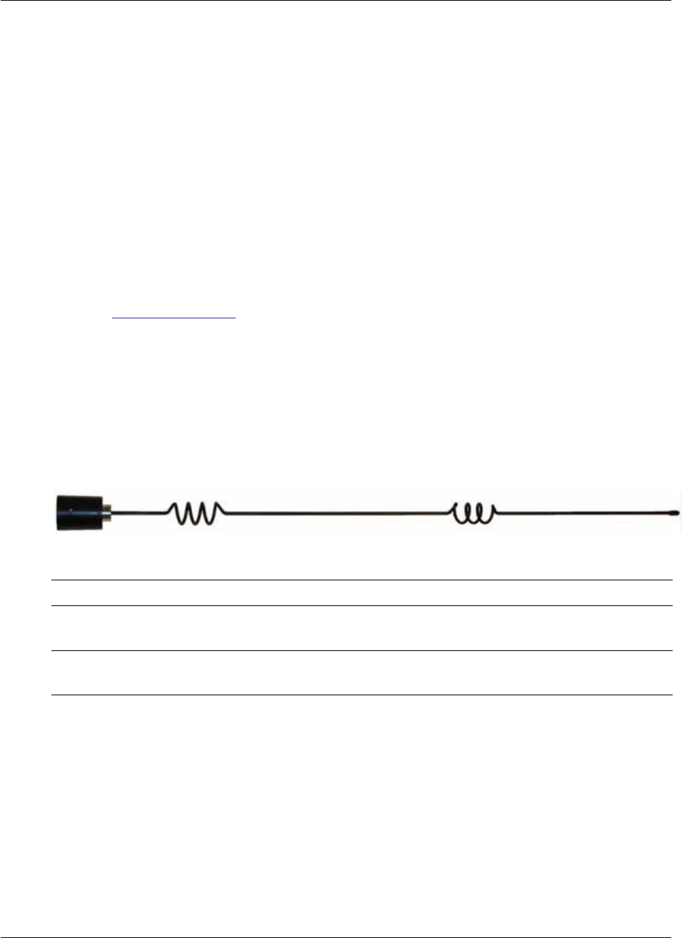
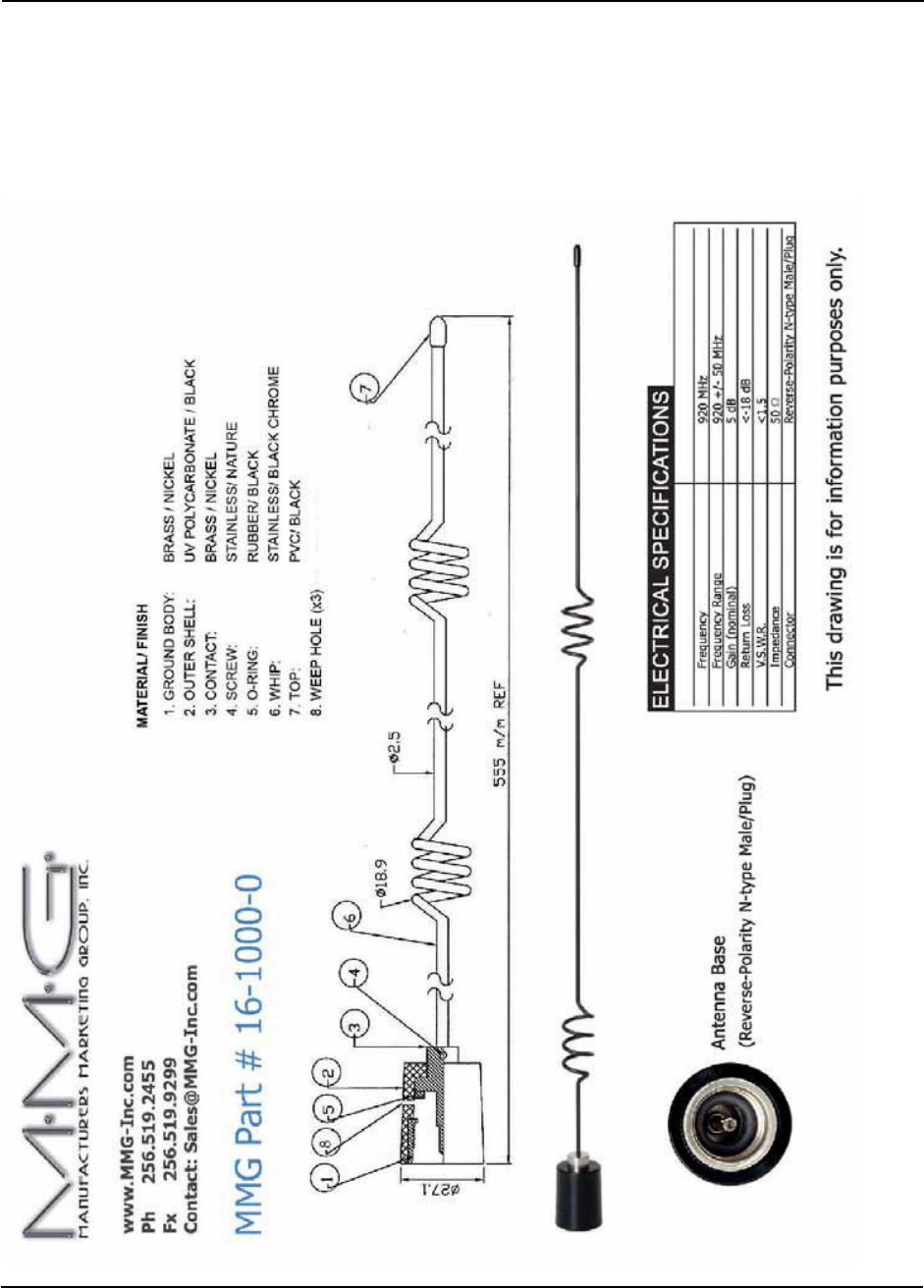
The external antenna used to qualify the board is an omnidirectional 5 dBi whip (shown in the
next figure), made by Manufacturers Marketing Group (MMG). The MMG part number for this
antenna is 16-1000-0. MMG contact information is on page 35. This antenna can be used, or any
other omnidirectional whip antenna with 5 dBi gain or less.
Figure 1 - 7. Whip Antenna with N-type Male Reverse-Polarity Connector
NOTE: See “External Antenna Specifications’ on page for antenna technical specifications.

Gridstream SCADA/DA S5SBR
98-2550 Rev AE 17
Landis+Gyr Quick Start Guide
1.14 Additional Specifications
Table 1 - 7. Additional Specifications
Category Specification Value(s) or Range(s)
Networking
Number of Channels 239 (narrow channel mode), 86 (wide channel mode) 51 UW, SUN 129
and 64
Channel Spacing 100 KHz (narrow channel mode), 300 KHz (wide channel mode) 200K
and 400K SUN
Modulation Type 2-FSK
RF Baud Rate 9.6, 19.2, 38.4, 115.2, 300 kbps. SUN 50,150 and 200kbps
FCC Operation Certification Part 15.247
Spreading Technique Frequency Hopping
Hopping Technique Pseudo Random Asynchronous
Hopping Patterns 65,536 (Unique per network)
Network Address Latitude / Longitude Coordinates
Turn-Around Time 100[uS] max
Programming
Programming Language Device Control Word (DCW)
Radio Firmware Version 5.72 later
Data
LAN Packet Port (LPP)
Serial Interface, DCW adjustable per specs below
Data Rate - 9.6, 19.2, 38.4, 115.2 kbps
Transparent Port (TPP)
Serial Interface, DCW adjustable per specs below
Data Rate - 9.6, 19.2, 38.4, 115.2 kbps
Serial Interface TTL
Parity Odd, Even, or None
Data bits 7 or 8
Stop bits 1 or 2
Duplex Full
Protocol Any asynchronous byte-oriented protocol
Environmental
Operating Temperature -40°C to +85°C
Storage Temperature -40°C to +85°C
Humidity 85C, 85% RH
Mechanical
Size
1.5x1.5
98-2550 Rev AE
18
Gridstream SCADA/DA S5SBR
Quick Start Guide Landis+Gyr
2 CONFIGURING AND TESTING
2.1 Connecting to a Gridstream S5 SBR Using Radio Shop
Connect the LAN Connect the LAN Packet Protocol port of your Gridstream S4SBR to your
computer's serial port using the USB cable. Once the Gridstream S5 SBR is powered up, you can
launch RadioShop on your computer. RadioShop will now connect to your local Gridstream S5
SBR card.
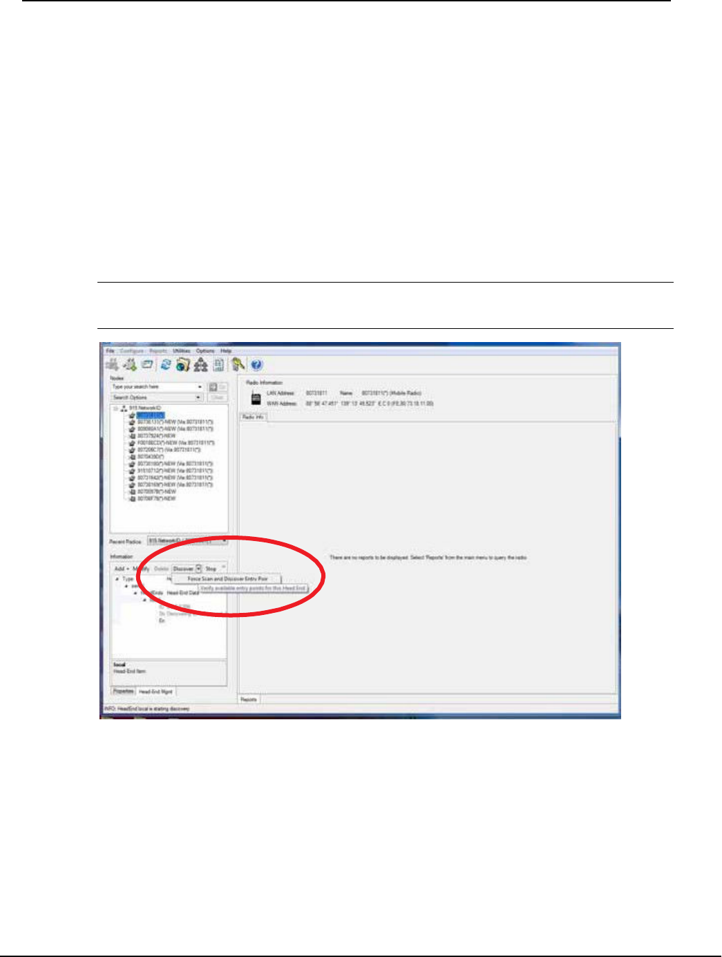
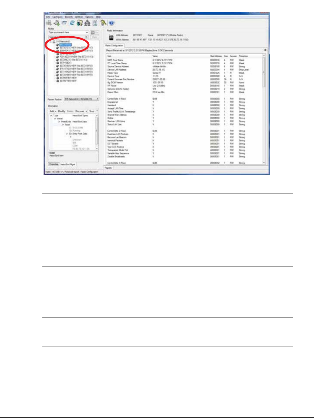
1. On the RadioShop home screen, click Discover | Force Scan and Discover Entry Ports.
NOTE: When the Select COM Ports for Discovery window opens, select the COM port on
your computer that is connected to the Gridstream S5 SBR, and then click OK.
Figure 2 - 1. Connecting to a Head-end Radio
Once connected, the local radio's LAN address will appear on the list at the top left-hand
side of the screen, and the radio configuration will be displayed in the main window
(Figure 2 - 1). This radio can now be used to communicate with the Gridstream S5 SBR
and configure it as needed.
Gridstream SCADA/DA S5SBR
98-2550 Rev AE 19
Landis+Gyr Quick Start Guide
Figure 2 - 2. Radio Configuration for Head-end Radio
NOTE: All RF Mesh radios ship with a default Network ID, or CRC, of 670. In order to
communicate with the Gridstream S5 SBR, your local radio will have to be re-configured to
match the Network ID (default 670) of the Gridstream S5 SBR.
After re-configuring the Gridstream S5 SBR to match the customer’s unique Network ID, the
local radio will need to be reset to its original Network ID. See below or see “Assigning a
New Network ID to a Gridstream S5 SBR” on page 26 for viewing the steps to re-configure
the local radio.
2.2 Assign the Network ID (CRC) of the Gridstream S5 SBR
All Gridstream SBRs ship with a default network ID, or CRC, of 670. In order to communicate
with other radios in a customer's network, the Gridstream S5 SBR will have to be re-configured
to match the customer's unique network ID.
NOTE: Prior to operation, a Network ID/CRC must be assigned. Network ID / CRC parameters
are unique and are assigned for each customer. Please call Landis+Gyr Customer Service if
you require a Network ID/CRC.
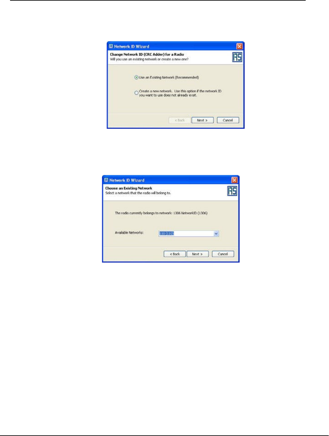
1. From the RadioShop home screen, select Configure | Change Network Id (CRC). The
Network ID Wizard dialog will open,
98-2550 Rev AE
20
Gridstream SCADA/DA S5SBR
Quick Start Guide Landis+Gyr
2. Select Use an Existing Network and click Next to continue.
Figure 2 - 3. Network ID Wizard
The Choose an Existing Network dialog is displayed.
Figure 2 - 4. Choose an Existing Network
3. Choose a Network ID from the Available Networks drop-down list.
4. Click Next to continue.
The Final Confirmation dialog is displayed.
Gridstream SCADA/DA S5SBR
98-2550 Rev AE 21
Landis+Gyr Quick Start Guide
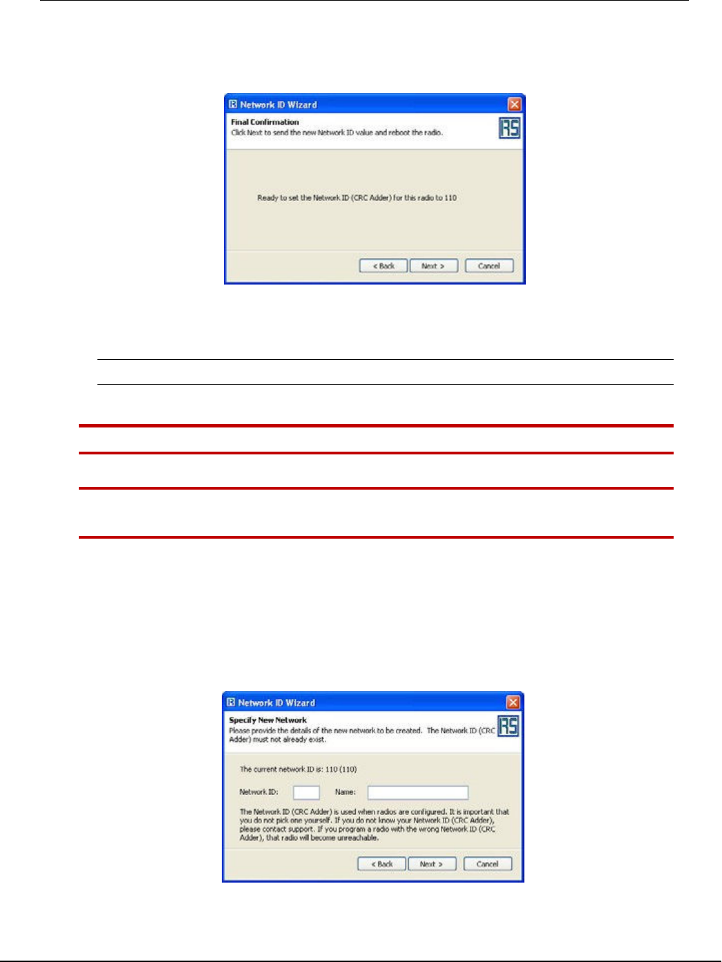
5. Click Next to change the Network ID for the Gridstream S5 SBR.
Figure 2 - 5. Final Confirmation Dialog
A confirmation message verifies that the Network ID has been changed.
NOTE: The Gridstream S5 SBR will reboot to complete the Network ID/CRC Change action.
2.3 Assigning a New Network ID to a Gridstream S5 SBR
WARNING: Assign a new Network ID only if the ID you want to use does not exist already.
WARNING: Valid values range from 1 to 65535. If 0 is displayed at startup, call Landis+Gyr
Customer Service.
To assign a new Network ID to a Gridstream S5 SBR, perform the following steps.
1. Select Configure > Network Id (CRC). The first dialog of the Network ID Wizard is displayed.
2. Select Create a New Network.
3. Click Next.
The Specify New Network dialog is displayed.
Figure 2 - 6. Specify New Network
98-2550 Rev AE
22
Gridstream SCADA/DA S5SBR
Quick Start Guide Landis+Gyr
4. Specify the Network ID and Name of the new network you want to assign.
5. Click Next to continue.
NOTE: Do not use spaces in the Name field.
The Final Confirmation dialog is displayed.
6. Click Next to create the Network ID for the Gridstream S5 SBR.
A confirmation message verifies that the new Network ID has been assigned to the Gridstream S5 SBR.
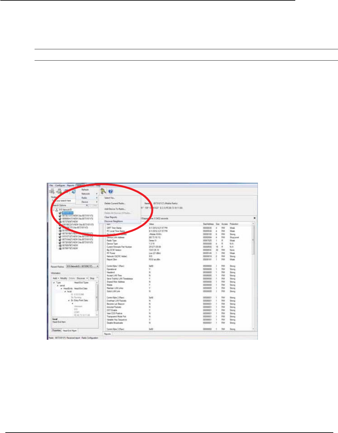
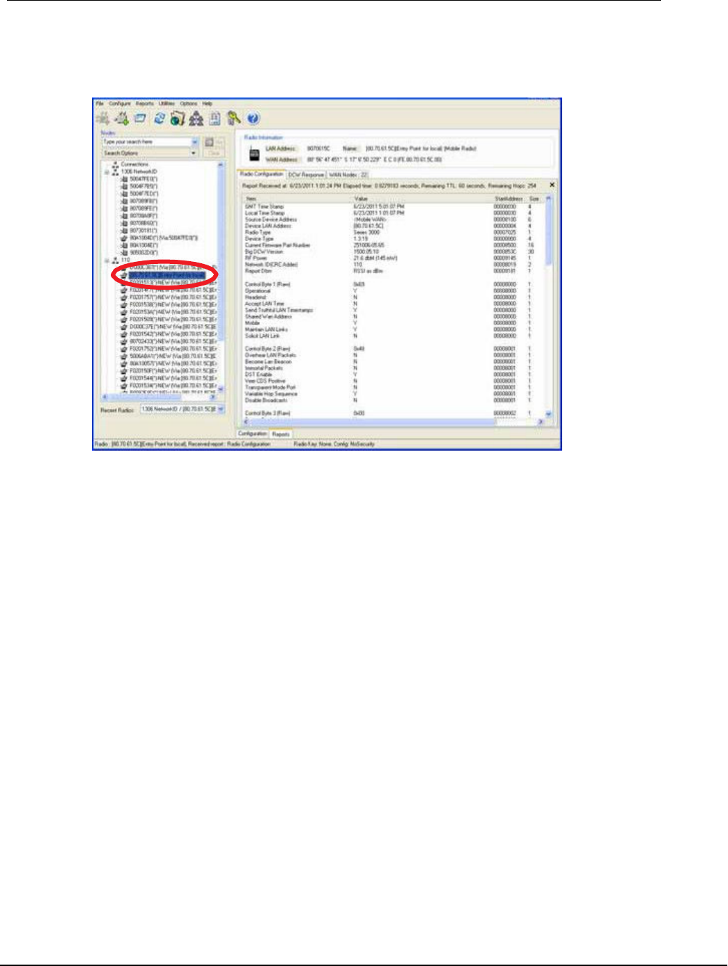
2.4 Adding New Radios to RadioShop
You can now add the Gridstream S5 SBR to the RadioShop database.
1. Confirm that your local radio is highlighted on the Nodes Pane.
2. Click the Generate WAN Nodes Report icon.
3. From the RadioShop home screen, click Utilities | Radio | Discover Neighbors, as shown in the figure
below.
Figure 2 - 7. Discovering Neighbors
Gridstream SCADA/DA S5SBR
98-2550 Rev AE 23
Landis+Gyr Quick Start Guide
4. Once discovered, the Gridstream S5 SBR’s LAN Address will appear in the Nodes pane, as shown in Figure 2
- 8.
Figure 2 - 8. Gridstream S4SBR’s LAN Address Appears in the Nodes Pane
5. Highlight the new Gridstream S5 SBR as shown in Figure 2 - 8, and click Reports | Configuration | Radio to
verify that you can communicate with the Gridstream S5 SBR.
6. Review the report to verify the radio’s firmware version and network ID.
98-2550 Rev AE
24
Gridstream SCADA/DA S5SBR
Quick Start Guide Landis+Gyr
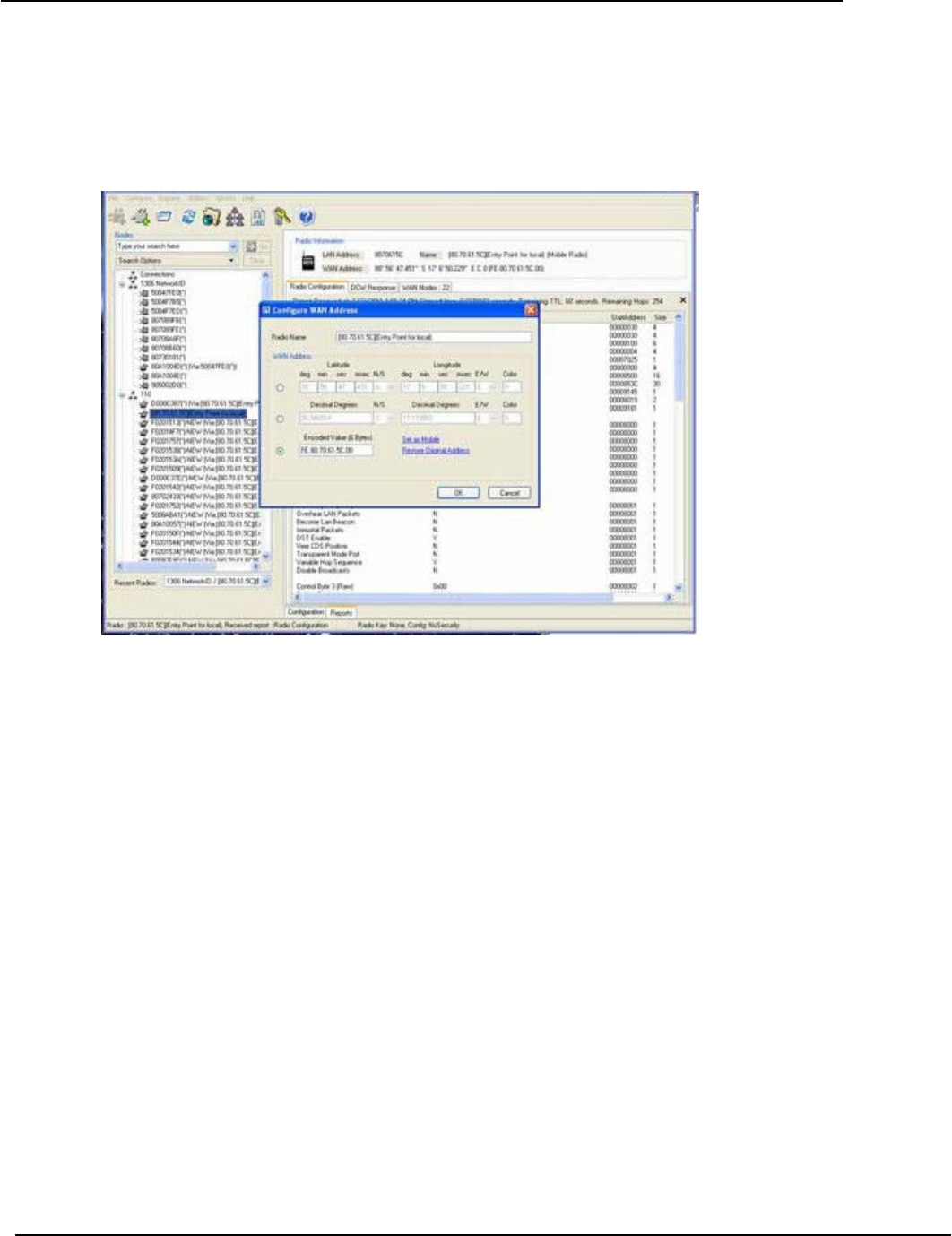
2.5 Setting the Latitude & Longitude
1. From the RadioShop home screen, click Configure | WAN Address.
2. In the Configure WAN Address window, specify the new coordinates, and click OK.
Figure 2 - 9. Configuring the WAN Address
A message will appear indicating that the radio was successfully programmed.

Gridstream SCADA/DA S5SBR
98-2550 Rev AE 25
Landis+Gyr Quick Start Guide
2.6 Troubleshooting
The Gridstream S5 SBR has been designed as a Field Replaceable Unit (FRU). As such, there are no serviceable
parts in the unit.
If you suspect parts within the Gridstream S5 SBR have failed:
1. Inspect the module to determine if there is any visual indication of damage to the unit.
2. Verify that power is being supplied to the unit. If the power is within operating parameters, proceed to
Step 3.
3. Try to connect with a locally connected Series-4 IWR configured the same as the Gridstream S5 SBR. If,
after five minutes, the locally connected Series-4 IWR does not acquire the Gridstream S5 SBR in its
neighbors list, the Gridstream S5 SBR should be replaced.
For additional assistance for this product, contact Landis+Gyr Technical Support at 1-888-390-5733 or
solutionsupport.na@landisgyr.com.
98-2550 Rev AE
26
Gridstream SCADA/DA S5SBR
Quick Start Guide Landis+Gyr
3 DEVELOPMENT ENVIRONMENT
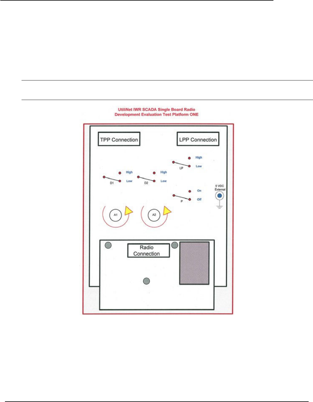
3.1 Gridstream SCADA/DA Series 5 Single Board Radio Interface Board
The Gridstream S5 SBR has been designed as a Field Replaceable Unit (FRU). As such, there are no serviceable
parts in the unit.
NOTE: The drawings provided in this section are for design reference purposes only. No interface board is
available for purchase from Landis+Gyr.
Figure 3 - 1. Board Component Layout
Gridstream SCADA/DA S5SBR
98-2550 Rev AE 27
Landis+Gyr Quick Start Guide
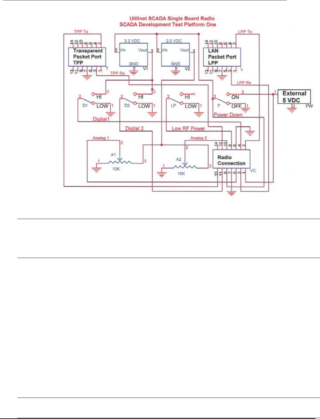
Figure 3 - 2. Board Components Schematic
NOTE: With the digital input switch tying the digital I/O pin on the Gridstream S5 SBR to either logic 0 or a logic
1 voltage level, this Development Test Platform One does not have functions to test the digital output of the
Gridstream S5 SBR. It is recommended to NOT configure the digital I/O pin as output when the Gridstream S5
SBR is connected to the test interface board.
3.2 Transparent Port (TPP) Connection
This connector is used to establish connection to the Gridstream S5 SBR through the transparent port. When
communication through the transparent port is desired, connect the USB cable to this connector.
3.3 LAN Packet Port (LPP) Connection
This connector is used to establish connection to the Gridstream S5 SBR through the LAN packet port. When
communication through the LAN packet port (using RadioShop) is desired, connect the USB cable to this
connector.
3.4 Onboard Regulator
The Gridstream S5 SBR interface board is equipped with an onboard VDC regulator. This regulator accepts a 4.0
~ 7.0 VDC input from a main power source and regulates it to power device electronics.
NOTE: The S5 SBR onboard VDC regulator is not capable of supplying power to additional devices beyond the
S5 SBR.

98-2550 Rev AE
28
Gridstream SCADA/DA S5SBR
Quick Start Guide Landis+Gyr
3.5 Digital Input
Digital input to Gridstream S5 SBR can be tested by toggling the two switches on the test board that
correspond to D1 for DIGITAL_IO1 and D2 for DIGITAL_IO2. The switch will toggle between 0V and supply VDC.
3.6 Analog Input
Analog input to the Gridstream S5 SBR can be tested by tuning the two potentiometers on the test board that
correspond to A1 for ANALOG_IN1 and A2 for ANALOG_IN2. The input voltage should lay between 0 VDC and
2.5 VDC.
NOTE: With an on-board reference 2.5 VDC, the highest analog input the Gridstream S5 SBR may sense is
limited to 2.5 VDC. Although the processor on the Gridstream S5 SBR may withstand supply VDC analog input,
users are advised not to exceed 2.5 VDC.
3.7 General Usage Instruction
Depending on the desired method used to establish communication, connect a USB cable to the Transparent
Packet Port (TPP), the LAN Packet Port (LPP) connection, or both.
NOTE: To provide power to the Gridstream S5 SBR test Platform, the power input must be supplied externally
(as shown) because the USB cable, when connected to the TPP or LPP connector, does not have provide power
for the test board.
Set the USB power input to an appropriate level by toggling the switch (P) controlling the *PWR_DN signal (pin
9) to OFF position.
Connect the Gridstream S5 SBR to the test board through the board-to-board I/O connector (located under the
SRB).
Toggle the switch (P) controlling the signal (pin 9) *PWR_DN to the ON position to turn the Gridstream S5 SBR
ON.
The switch (LP) controlling *LOW_RF_POWER may be toggled to set (pin 8) the transmit level of the Gridstream
S5 SBR under test. This switch will control whether to transmit with limited or full power.

Gridstream SCADA/DA S5SBR
98-2550 Rev AE 29
Landis+Gyr Quick Start Guide
3.8 Gridstream S5 SBR Logic
Developers planning to use the Gridstream SCADA/DA Series 5 Single Board Radio (Gridstream S5 SBR) in
their SCADA equipment as a monitoring device should be aware of the logic of the setting when writing a
DCW program. The following describes the logic for reading and writing Gridstream S5 SBR Control Registers
1 and 2 located at memory locations 7700h and 7700h in the
radio using a DCW.
3.8.1
Control Register 1
D1-Input
Pin D1 at 7700h (Bits 0-3), if 7700h (Bit 0 = “0”) Input then read Control at 7700h (Bits 2-3)
• If Control = “00” - General Purpose => Read state at 7700h (Bit 1) and report
• If Control = “01” - Rising Edge => Read count at 7706h (four bytes) and report
• If Control = “10” - Falling Edge => Read count at 7706h (four bytes) and report
• If Control = “11” - Either Edge => Read count at 7706h (four bytes) and report
D1-Output
Pin D1 at 7700h (Bits 0-3), if 7700h (Bit 4 = “0”) Output then verify Control = “00”
• If NOT “00” => Report Error in configuration
• If “00” General Purpose => Set state at 7700 (Bit 1) and report
Pin D2 at 7700h (Bits 4-5), if 7700h (Bit 4 = “0”) Input then read state at 7700 (Bit 5) and report
D2-Input
Pin D2 at 7700h (Bits 4-5), if 7700h (Bit 4 = "0") Input then read state at 7700 (Bit 5) and report
D2-Output
Pin D2 at 7700h (Bits 4-5), if 7700h (Bit 4 = “1”) Output then set state at 7700 (Bit 5) and report

98-2550 Rev AE
30
Gridstream SCADA/DA S5SBR
Quick Start Guide Landis+Gyr
3.8.2
Control Register 2
A1-Input
Pin A1 at 7701h (Bits 0-2), if 7701 (Bit 0 = “0”) Input then read Control at 7701h (Bit 2)
• If Control = “0” - General Purpose => Read state at 7701h (Bit 1) and report
• If Control = “1” - Analog to Digital Channel => Read channel at 7702h (2 bytes) and report
A1-Output
Pin A1 at 7701h (Bits 0-2), if 7701 (Bit 0 = “1”) Output then read Control at 7701h (Bit 2)
• If Control = “0” - General Purpose => Set state at 7701h (Bit 1) and report
• If Control = “1” - Analog to Digital Channel => Report Error in configuration
A2-Input
Pin A2 at 7701h (Bits 4-6), if 7701 (Bit 4 = “0”) Input then read Control at 7701h (Bit 6)
• If Control = “0” - General Purpose => Read state at 7701h (Bit 5) and report
• If Control = “1” - Analog to Digital Channel => Read channel at 7704h (2 bytes) and report
A2-Output
Pin A2 at 7701h (Bits 4-6), if 7701 (Bit 0 = “1”) Output then read Control at 7701h (Bit 6)
• If Control = “0” - General Purpose => Set state at 7701h (Bit 5) and report
• If Control = “1” - Analog to Digital Channel => Report Error in configuration

Gridstream SCADA/DA S5SBR
98-2550 Rev AE 31
Landis+Gyr Quick Start Guide
3.9 Digital I/O Functionality
NOTE: This device provides two general purpose digital I/O lines. These are controllable through the DCW
programming language. It is outside the scope of this document to describe that language but, in brief, there
are mechanisms by which each line can be independently configured as input or output.
The state of inputs can be read, and the state of outputs can be set. DCW code execution operates as a virtual
environment and, as such, does not support rapid transitions. Users should understand the speed limitations
associated with the use of these digital I/O pins.
The register below can be used to control either of the two general purpose I/O pins (D1 & D2) located at
memory location 7700 (hex).
Table 3 - 1. Control Register 1
Bit Feature Description Dflt.
0
Pin D1 Direction 0: Input
1: Output
0
1
Pin D1 State
When D1, bit 0 is "0" and bit 2-3 is "00", then bit 1 returns current state
as "0" or "1".
When D1, bit 0 is "0" and bit 2-3 is not "00", then read location 7706-
7709 which returns the count of the as defined in bit 2-3.
When D1, bit 0 is "1" then the value can be read or set.
0
2-3
Pin D1 Control
00: General Purpose I/O
01: Count interrupts on rising edge
10: Count interrupts on falling edge
11: Count interrupts on either edge
0
4
Pin D2 Direction 0: Input
1: Output
0
5
Pin D2 State When D2, bit 4 is "0" then bit 5 returns current state as "0" or "1".
When D2, bit 4 is "1" then the value can be read or set.
0
6-7 Reserved N/A 0
Landis+Gyr
32 98-2550 Rev AE Gridstream SCADA/DA S4SBR
3.10 Analog Input Functionality
This device provides two general purpose analog inputs. These are filtered and connected to a
10-bit A/D converter.
NOTE: The voltage reference for this A/D converter is 2.5 VDC +/- 60[mVDC] across the
operating temperature range.
This A/D converter has the following specifications:
Table 3 - 2. A/D Converter Specifications
A/D characteristic Specification
Resolution 10 bit
INL +/-5 LSB
Absolute Accuracy +/-5 LSB
DNL +/-1 LSB
Offset Error +/-3 LSB
Gain Error +/-3 LSB
NOTE: The actual sampling time is 0.25 μS and the conversion time is 2.75 μS, but the rate at
which signals on these inputs can be sampled in-practice is limited by the DCW execution. It is
recommended that these channels be used only for DC voltage measurement, and that the
sampling rate cannot exceed 100 mS.

Landis+Gyr
Gridstream SCADA/DA S4SBR 98-2550 Rev AC 33
The register below can be used to control either of the two general purpose Analog pins (A1 &
A2) located at memory location 7701 (hex).
Table 3 - 3. Control Register 2
Bit Feature Description Dflt.
0
Pin A1 Direction 0: Input
1: Output
0
1
Pin A1 State
When A1, bit 0 is "0" and bit 2 is "0", then bit 1 returns current state as
"0" or "1".
When A1, bit 0 is "0" and bit 2 is "1", then read location 7702-7703
which returns the Hex value of the sampled voltage between 0-2.5
VDC.
When A1, bit 0 is "1", then the value of bit 1 can be set.
0
2
Pin A1 Control 0: General Purpose I/O
1: Analog to Digital Channel (Bit 0 = "0" only)
0
3 Reserved Not Used 0
4
Pin A2 Direction 0: Input
1: Output
0
5
Pin A2 State
When A2, bit 4 is "0" and bit 6 is "0", then bit 5 returns current state as
"0" or "1".
When A2, bit 4 is "0" and bit 6 is "1", then read location 7704-7705
which returns the Hex value of the sampled voltage between 0-2.5
VDC.
When A2, bit 4 is "1", then the value of bit 5 can be set.
0
6
Pin A2 Control 0: General Purpose I/O
1: Analog to Digital Channel (Bit 0 = "0" only)
0
7 Reserved Not Used 0

Landis+Gyr
34 98-2550 Rev AE Gridstream SCADA/DA S4SBR
3.11 Memory Location
Memory locations in the S4SBR [listed above in Table 3-3 and below as 77XX-77XXx] store
commands to control (as outputs) and monitor the status (as inputs) of connected devices.
[7702-7703h] Analog to Digital Channel A1.
When A1 is set to “Analog to Digital” (Bit 2) this location will contain a 10-bit reading. The
scale on this board is from 0 to 2.5 volts. Voltages greater than 2.5 VDC will be reported as 2.5
VDC.
[7704-7705h] Analog to Digital Channel A2.
When A2 is set to “Analog to Digital” (Bit 6) this location will contain a 10-bit reading. The
scale on this board is from 0 to 2.5 volts. Voltages greater than 2.5 VDC will be reported as 2.5
VDC.
[7706-7709h] D1 Interrupt Counter.
If D1 is configured as an interrupt (Bit 2-3) then this location will count the number of
interrupts that
have been detected.
NOTE: The interrupt counter is cleared each time interrupts are enabled.
Landis+Gyr
Gridstream SCADA/DA S4SBR 98-2550 Rev AC 35
APPENDIX A. EXTERNAL ANTENNA
Manufacturer Contact Information
Manufacturers Marketing Group,
Inc.
922-C Merchants Walk
Huntsville, AL 35801
Phone: 256-519-2455
Fax: 256-519-9299
Website: www.mmg-inc.com
External Antenna Specifications
The external antenna used to qualify the board is an omnidirectional 5 dBi whip (shown in the
next figure), made by MMG. The MMG antenna part number is 16-1000-0. See page 48 for
product data sheet.
Figure A - 1. Whip Antenna with N-type Male Reverse-Polarity Connector
NOTE: This antenna’s maximum gain is 5 dBi and its efficiency is 80%
NOTE: Any antenna may be used as long as it is an omnidirectional whip with a gain of 5
dBi or
less.
Landis+Gyr
36 98-2550 Rev AE Gridstream SCADA/DA S4SBR
Ground Plane Specifications
NOTE: Please note this antenna equires a ground plane (MMG P/N 17-1000-A). The ground
plane should be at least six inches in diameter. See Figure A - 2
“
“
Figure A - 2. Ground Plane Specification
If the enclosure for the board is metal and at least 6" across, and the antenna is connected
directly to the enclosure, no ground plane is required, as the enclosure is the ground plane.
The radiation pattern of the recommended antenna is of a traditional dipole (RF pattern as a
donut). The orientation of the antenna should be in the vertical position (straight up or
straight down), such that the RF pattern is omni-directional in the horizontal plane.

Landis+Gyr
Gridstream SCADA/DA S4SBR 98-2550 Rev AC 37
RF Antenna Specifications
An external antenna is connected to the board via an RF coaxial cable of the type as
shown in Figure
A - 3.
Figure A - 3. RF Coaxial Cable
The cable has a Female R-SMA connector on one end and an U.FL Female connector
on the other. This cable is suppled in order to make the interconnect between the
radio card and the Coax cable leading to the external antenna , you will need to
make a R-SMA Male to N Type coax cable to the antennas location.
Landis+Gyr
38 98-2550 Rev AE Gridstream SCADA/DA S4SBR
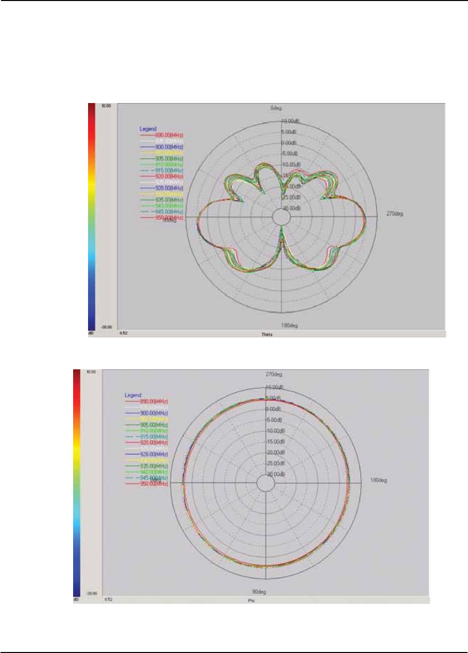
External Antenna Radiation Pattern
The antenna's radiation pattern is shown in Figure A - 4 and Figure A - 5.
Figure A - 4. External Antenna Radiation Pattern, Side View
Figure A - 5. External Antenna Radiation Pattern, Top View

Landis+Gyr
Gridstream SCADA/DA S4SBR 98-2550 Rev AC 39
APPENDIX B. FCC AND INDUSTRY CANADA COMPLIANCE
FCC Class B
This device complies with Part 15 of the FCC rules. Operation is subject to the
following two conditions:
1. This device may not cause harmful interference, and
2. This device must accept any interference received, including
interference that may cause
undesired operation.
This equipment has been tested and found to comply with the limits for a Class B
digital device,
pursuant to Part 15 of the FCC Rules. These limits are designed to
provide reasonable protection
against harmful interference in a residential
installation. This equipment generates, uses, and can
radiate radio frequency
energy and, if not installed and used in accordance with the Instructions, may
cause
harmful interference to radio communications. However, there is no guarantee that
interference will not occur in a particular installation. If this equipment does cause
harmful
interference to radio or television reception, which can be determined by
turning the equipment off and on, the user is encouraged to try to correct the
interference by one or more of the following
measures:
• Reorient or relocate the receiving antenna.
• Increase the separation between the equipment and receiver.
• Consult Landis+Gyr or an experienced radio technician for help.
Υ
WARNING: Changes or modifications to this device not expressly approved
by Landis+Gyr could void the user's authority to operate the equipment.
RF Exposure
This equipment complies with FCC/IC radiation exposure limits set forth for an
uncontrolled
environment. This equipment should be installed and operated with
minimum distance of 27 centimeters between the radiator and your body. This
transmitter must not be co-located or operating
in conjunction with any other
antenna or transmitter.
Cet équipement est conforme aux limites FCC/IC d'exposition aux radiations définies
pour un environnement non contrôlé. Cet équipement doit être installé et utilisé à
une distance minimale de 27cm entre le radiateur et votre corps. Cet émetteur ne
doit pas être co-implantés ou exploités en conjonction avec une autre antenne ou
émetteur.

Landis+Gyr
40 98-2550 Rev AE Gridstream SCADA/DA S4SBR
Industry Canada
This device complies with Industry Canada license-exempt RSS standard(s).
Operation is subject to the following two conditions: (1) this device may not cause
interference, and (2) this device must accept any interference, including
interference that may cause undesired operation of the device.
Under Industry Canada regulations, this radio transmitter may only operate using
an antenna of a type and maximum (or lesser) gain approved for the transmitter
by Industry Canada. To reduce potential radio interference to other users, the
antenna type and its gain should be so chosen that the equivalent isotropically
radiated power (e.i.r.p.) is not more than that necessary for successful
communication.
This radio transmitter (DEVICE IC 5294A-NG0R1S3) has been approved by Industry
Canada to operate with the antenna types listed below with the maximum
permissible gain and required antenna impedance for each antenna type
indicated. Antenna types not included in this list, having a gain greater than the
maximum gain indicated for that type, are strictly prohibited for use with this
device.
Approved Antenna: Omni-directional antenna, 5 dBi gain, 902-928 MHz, antenna
impedance is 50 ohms.
Le présent appareil est conforme aux CNR d'Industrie Canada applicables aux
appareils radio exempts de licence. L'exploitation est autorisée aux deux
conditions suivantes : (1) l'appareil ne doit pas produire de brouillage, et (2)
l'utilisateur de l'appareil doit accepter tout brouillage radioélectrique subi, même
si le brouillage est susceptible d'en compromettre le fonctionnement.
Conformément à la réglementation d'Industrie Canada, le présent émetteur radio
peut fonctionner avec une antenne d'un type et d'un gain maximal (ou inférieur)
approuvé pour l'émetteur par Industrie Canada. Dans le but de réduire les risques
de brouillage radioélectrique à l'intention des autres utilisateurs, il faut choisir le
type d'antenne et son gain de sorte que la puissance isotrope rayonnée
équivalente (p.i.r.e.) ne dépasse pas l'intensité nécessaire à l'établissement d'une
communication satisfaisante.
Le présent émetteur radio (DEVICE IC 5294A-NG0R1S3) a été approuvé par
Industrie Canada pour fonctionner avec les types d'antenne énumérés ci-dessous
et ayant un gain admissible maximal et l'impédance requise pour chaque type
d'antenne. Les types d'antenne non inclus dans cette liste, ou dont le gain est
supérieur au gain maximal indiqué, sont strictement interdits pour l'exploitation
de l'émetteur.

Landis+Gyr
Gridstream SCADA/DA S4SBR 98-2550 Rev AC 41
Host FCC Label Requirement
In the final installation, the following information must be visible:
• Contains FCC ID: R7PNG0R1S3
• Contains IC: 5294A-NG0R1S3
• Module Model: S5 SBR
This device complies with Part 15 of the FCC rules. Operation is subject to the
following two conditions:
1. This device may not cause harmful interference.
2. This device must accept any interference received, including interference
that may cause undesired operation.
Landis+Gyr
42 98-2550 Rev AE Gridstream SCADA/DA S4SBR
APPENDIX C. MMG DATA SHEET