Larcan DTR10SC Digital Television Translator User Manual service manual
Larcan Inc Digital Television Translator service manual
Larcan >
Contents
- 1. Installation and operating manual
- 2. service manual
service manual

PUBLICATION TSM 20-399
TECHNICAL MANUAL
10 WATT VHF AMPLIFIER
FOR FRONTIER SERIES
DIGITAL TV TRANSMITTER/TRANSLATOR
LARCAN INC.
228 AMBASSADOR DRIVE
MISSISSAUGA, ONTARIO
CANADA L5T 2J2
PHONE: (905) 564-9222
FAX: (905) 564-9244
Rev 0 Feb 2014
TSM 20-399 Rev 0, Feb 2014 1 10W VHF Amplifier
CONTENTS
1 GENERAL .......................................................................................................................................................................... 3
1.1 SAFETY NOTICES .......................................................................................................................................................... 3
1.1.1 Beryllium Oxide Warning .................................................................................................................................... 3
1.1.2 Other Toxic Materials .......................................................................................................................................... 3
1.1.3 Dangerous Voltages ............................................................................................................................................. 3
1.1.4 Switch to Safety .................................................................................................................................................... 4
1.2 STATIC AWARENESS ..................................................................................................................................................... 5
1.3 TRADEMARK INFORMATION .......................................................................................................................................... 6
1.4 PRODUCTION CHANGES ................................................................................................................................................ 6
2 INTRODUCTION.............................................................................................................................................................. 7
2.1 AMPLIFIER CHAIN ......................................................................................................................................................... 7
3 MASK FILTER AND OUPTPUT .................................................................................................................................... 8
3.1 HELICAL RESONATOR BANDPASS FILTER ...................................................................................................................... 8
3.2 LOW POWER FILTER FOR HIGH BAND ........................................................................................................................... 9
3.3 LOW PASS AND NOTCH FILTER FOR LOW BAND ............................................................................................................ 9
3.4 RF DIRECTIONAL COUPLER ......................................................................................................................................... 10
4 RF POWER AMPLIFIER AND HEATSINK ASSEMBLY ........................................................................................ 18
4.1 PREAMPLIFIER ............................................................................................................................................................. 18
4.2 OUTPUT AMPLIFIER ..................................................................................................................................................... 18
5 METERING AND CONTROL ....................................................................................................................................... 24
5.1 SYSTEM ...................................................................................................................................................................... 24
5.2 RF DETECTORS ........................................................................................................................................................... 24
5.3 RF METERING BOARD CALIBRATION .......................................................................................................................... 24
5.3.1 Forward Power Meter Calibration - Zero Adjust .............................................................................................. 24
5.3.2 Reflected Power Meter Calibration - Zero Adjust ............................................................................................. 24
5.3.3 Forward Power Calibration .............................................................................................................................. 25
5.3.4 Reflected Power Calibration .............................................................................................................................. 25
TSM 20-399 Rev 0, Feb 2014 2 10W VHF Amplifier
LIST OF FIGURES
Figure 1 Bandpass Filter Response ...........................................................................................................................8
Figure 2 Bandpass Filter Schematic ...........................................................................................................................9
Figure 3 RF Directional Coupler Schematic .............................................................................................................11
Figure 4 Generic Helical Resonator Bandpass Filter Assembly ..............................................................................12
Figure 5: Filter Schematic .........................................................................................................................................13
Figure 6 Low Band Bandpass and Notch Filter Assembly ........................................................................................14
Figure 7 Low Band Bandpass and Notch Filter Schematic .....................................................................................15
Figure 8 RF Directional Coupler ...............................................................................................................................16
Figure 9 Low Band Coupler PC Board Assembly .....................................................................................................17
Figure 10: Preamplifier Assembly .............................................................................................................................19
Figure 11: Preamplifier Schematic............................................................................................................................20
Figure 12: Final Amplifier Assembly (sht 1) ..............................................................................................................21
Figure 13: Final Amplifier Assembly (sht 2) ..............................................................................................................22
Figure 14: Final Amplifier Schematic ........................................................................................................................23
Figure 15: System Block Diagram ............................................................................................................................26
Figure 16:Metering Board Assembly.........................................................................................................................27
Figure 17: Metering Board Schematic ......................................................................................................................28
TSM 20-399 Rev 0, Feb 2014 3 10W VHF Amplifier
1 GENERAL
1.1 SAFETY NOTICES
This section has been written to provide general guidance and information for the operation, maintenance, and service
personnel who are familiar with the hazards of working with high-powered and high-voltage electronic circuits. This
manual does not detail all of the safety precautions which should be observed when servicing this or any other
electronic equipment. Service by inadequately trained or inexperienced personnel can result in personal injury
or death and/or damage to the equipment.
Important: All personnel concerned with the servicing of equipment should be thoroughly familiar with standard first
aid procedures for the treatment of electrical burns and shock, including cardio-pulmonary resuscitation (CPR).
Use the “buddy” system, with one person performing the actual service and a colleague observing. The observer must
be familiar with the work being performed and within sight and sound of the person doing the work. The observer
should not be engaged in any other work or be otherwise distracted; he must be available instantly in case of
accident.
Always have the observer with you when you work on the transmitter.
1.1.1 Beryllium Oxide Warning
Internal thermal management in certain RF devices in this equipment is accomplished through the use of Beryllium
Oxide ceramic material. Beryllium Oxide is a hard white ceramic used as insulation for heatsinking of RF power
semiconductors. It is used between the silicon die of the device and the case, or flange, to both insulate and to conduct
heat to the heatsink through the flange of the transistor. Beryllium Oxide is a poison. Do not break open any RF power
transistors or otherwise dismantle them. In case of accidental breakage of devices, do not inhale the resulting
beryllium dust and avoid getting beryllium dust in your mouth. Do not let beryllium into your blood stream
through cuts or open wounds. Seek immediate medical attention if the dust enters your body in any manner. Avoid
cuts by wearing gloves while picking up the broken pieces. Be careful – do not inhale dust while replacing or emptying
vacuum cleaner filter bags and wash your hands thoroughly afterward. Wash your hands thoroughly after replacing RF
power devices. Dispose of defective RF power devices only through approved toxic waste facilities. Wear gloves when
picking up the pieces. Wash your hands thoroughly after replacing devices. Dispose of defective devices only through
approved toxic waste facilities.
Note: the ceramic cap that makes up the visible part of an RF device is not made from Beryllium Oxide. Beryllium Oxide
is only used internally to the device. While a broken ceramic cap can be sharp and cause cuts and abrasions and it is
therefore wise to handle it with care, the Beryllium Oxide is the substance used between the die of the device and the
internal case or flange.
When cleaning up after an accidental breakage, remember to wear a respirator mask to avoid inhaling the dust while
replacing or emptying vacuum cleaner filter bags, and to wash your hands well after servicing the vacuum cleaner. If
possible, use a wet vacuum, in which the dust gets trapped in water.
1.1.2 Other Toxic Materials
The non-metallic coverings of some coaxial cables used in this equipment are flammable and can transmit fire when
ignited. Other wire coverings are not capable of supporting combustion but any non-metallic covering when heated
sufficiently can emit dense smoke and acid gases, which can be highly toxic and often corrosive.
Solvents and glues can emit toxic vapors and can be flammable. Read and understand the directions on the containers
and ensure that they are used only in well ventilated locations.
1.1.3 Dangerous Voltages
LARCAN equipment has been designed to protect operating personnel from accidental contact with dangerous voltages,
by means of shields and covers. It is extremely important that any protective covering devices be kept in place at all times.
TSM 20-399 Rev 0, Feb 2014 4 10W VHF Amplifier
While all practical safety precautions have been adopted to safeguard personnel from possible injury, both supervisory
and operating personnel are urged to ensure that the safety rules detailed below are followed as an established routine at
all times. The following four Rules are the standard safety guidelines for working with and around transmitters:
Rule #1 KILL THE AC POWER BEFORE IT KILLS YOU
Under no circumstances should any person reach within the cabinets for the purpose of servicing or adjusting the
equipment without first disconnecting the AC power or without the immediate presence of another person
capable of rendering aid. The “buddy” system is encouraged for transmitter work.
Rule #2 DO NOT TAMPER WITH INTERLOCKS OR SAFETY SHIELDS
Under normal circumstances, no safety shield should be removed.
Rule #3 REMOVE PERSONAL JEWELRY WHEN WORKING ON THE EQUIPMENT
The mains AC power to this transmitter can deliver high currents capable of melting metallic tools or personal
jewelry, such as watch bands, bracelets, or rings. Accidental short circuits from such metallic objects can cause
an explosive shower of molten metal which can result in serious personal injury.
Rule #4 KNOW FIRST AID AND KEEP FIRST AID SUPPLIES AVAILABLE
Illustrated first aid instructions for the treatment of electrical shock and burns and CPR procedures should be
displayed in a prominent location adjacent to the equipment. In rendering first aid, the timeliness and
effectiveness of the treatment are vitally important to the recovery of the injured person.
Always have a colleague with you when you work on the transmitter and make sure both of you know first aid,
including cardio-pulmonary resuscitation (CPR). This is most important.
Without exception, all personnel should thoroughly familiarize themselves with the procedures involved. One person,
whose normal duties place him or her at the transmitter site often, should be given complete responsibility and authority to
ensure that first aid supplies are kept on site and maintained. Prominently display a list of emergency phone numbers.
This list should include the numbers of the nearest police, ambulance, hospital, doctor, fire department, paramedics,
poison control center, public works (roads) department, and the utility (power and phone) companies.
Do not try to work on the transmitter if you are tired or drowsy; you could make a fatal error in judgment. Antihistamines
and decongestants for colds or allergies, and some prescription medications, can make you drowsy; ask your pharmacist
if you do not know for sure. Avoid alcohol, even in moderate amounts, before working on the transmitter.
1.1.4 Switch to Safety
Here are some safety suggestions, based partially on the knowledge of experts familiar with high-powered tubed
equipment, and partially on the procedures used at a typical utility company and at a company which makes and tests
high voltage devices. A few of these suggestions apply primarily to factory environments and require some modification
to be applied in transmitter settings.
Our thanks to the Varian Corporation for sharing its "Electrical Safety Training Program" notes. Our thanks also to
Ontario Hydro for its information booklets dealing with high voltage.
MAKE SURE YOU HAVE IN PLACE A COMPREHENSIVE SAFETY PROGRAM AND HAVE DEFINED
PROCEDURES FOR EVERY ACTIVITY IN IT. KNOW FIRST AID AND CPR.
Use the “buddy” system, with one person performing the actual service and a colleague observing. The observer must
be familiar with the work being performed and within sight and sound of the person doing the work. The observer
should not be engaged in any other work or be otherwise distracted; he must be available instantly in case of
accident. Always have the observer with you when you work on the transmitter.
Keep the area neat and tidy, free of any interfering conductive material and free of any sharp objects. Remember that
reaction to a shock could cause you to strike nearby objects.
Avoid wearing loose clothing and personal jewelry such as rings, watches, and chains when working near energized
TSM 20-399 Rev 0, Feb 2014 5 10W VHF Amplifier
circuits. Make a habit of removing all jewelry and storing it in a safe place as soon as you enter the transmitter building.
Before beginning work, shut off all AC to the transmitter power supplies. Tag and lockout the switches. Your
safety routine must ensure that the person placing the tag and locking the switch is be the only person who removes it
and reactivates the switch. You might want to include the AC to the remote control as well, if there is any possibility that
a studio worker could unknowingly activate the transmitter while you are working on it. One way of ensuring that the
lockout "placer and remover" are the same person is to issue individual padlocks to each person on the transmitter
technical staff.
You might want to include your tower contractor's rigging crew in the list of people who are allowed to use tags and
padlocks. As an alternative, Dielectric™ makes a transmission line lockout switch intended for riggers to turn off and
lock out any RF before climbing over the antenna to replace light bulbs, etc.
Proper grounding is vital. Make ground inspection a part of your maintenance program; someone's life could depend
on it!
1.2 STATIC AWARENESS
Care must be taken at all times because this equipment contains static-sensitive MOS and FET devices. The following
information on static is particularly pertinent to CMOS and other MOS device handling.
1. It is important to avoid surroundings or situations in which static can be generated. The building floor should have
grounded conductive floor coverings or a grounded conductive mat placed on the floor in front of the bench. The
bench itself should also have a grounded conductive mat on which the equipment is placed. Anybody working on
the equipment should wear either a grounded wrist strap (preferable) or conductive overshoes. Vacuum cleaner
tools should all be conductive and grounded to avoid static from air motion. (Vacuum cleaners made for computer
servicing would be suitable). Soldering iron tips must be grounded. Use properly maintained soldering equipment
that has a three-wire grounding plug, verifying low path resistance between ground and the tip with an ohmmeter
every time this equipment is used.
2. The average person wearing rubber-soled shoes and walking across a woolen or synthetic carpet or untreated
vinyl tiled floor is able to generate voltages in excess of 15 to 20kV. Most MOS devices will suffer puncture of the
oxide insulating their gates, at 20 to 40V. Many CMOS devices are fabricated with built-in Zeners which will clamp
foreign voltages, but the amount of energy that must be dissipated can easily exceed the rating of this protection.
You should therefore assume that little or no static protection exists in a CMOS device and that you must provide
your own.
3. A typical unprotected gate of a CMOS logic IC has an input capacitance of about 5pF and can self-immolate at
20V, so the energy to destroy the IC is given by the expression W = CV2/2, where W is in watt-seconds, C is in
farads, and V is in volts. One watt-second is also known as a Joule. Substituting numeric quantities results in W =
5 x 10-12 x 20 x 20 ¸ 2 = 1 x 10⁻⁹ Joule per gate. Stored energy in the approximately 100pF capacitance of the
human body charged to 15kV, becomes W = 100 x 10-12 x 15000 x 15000 /2 = 11.25 x 10⁻³ Joule. Eleven and a
quarter million times more energy than is needed to destroy one gate input!
4. To avoid destroying CMOS devices, the human body must be grounded first. This is the reason for all the
"grounded surroundings" suggested in paragraph 1. Always ground yourself first, then the board.
5. Avoidance of static exposure of circuits and CMOS devices is easier. Ensure that board assemblies are always
kept in conductive bags or boxes when not in place in the equipment, and that spare CMOS ICs and devices are in
conductive chip carriers or plugged into conductive foam. Be careful about this point; many plastic foams can be
colored black, but may still be an insulator. Use an ohmmeter to be sure.
6. Identical statements to those made in the above paragraphs apply to RF power MOSFETs and although the gates
of these devices might appear to be considerably more robust than those of the average CMOS logic device, this
is due only to the much greater gate area and consequently greater input capacitance. The same order of
magnitude of gate oxide breakdown voltage exists for RF power FETs as for small CMOS devices, therefore use
the same care in handling.

TSM 20-399 Rev 0, Feb 2014 6 10W VHF Amplifier
1.3 TRADEMARK INFORMATION
All material in this manual is copyright LARCAN INC. and reproduction in whole or in part in any form for any purpose
other than exclusive use of the equipment owner, without prior written authorization from LARCAN INC., is prohibited.
Trademarks used in this document are the property of their respective owners and are mentioned in the text for
discussion purposes; any such mention is not necessarily an endorsement of the trademark or its owner.
Although the following pages contain as much information as is reasonably possible to provide, these instructions do
not purport to cover all details or variations in equipment nor to provide for every possible contingency to be met. It is
assumed that fully competent technical personnel will be responsible for the maintenance and repair of the equipment
that is described in this manual. If more information is required, contact:
LARCAN INC.
228 Ambassador Drive,
Mississauga, Ontario, Canada L5T-2J2.
Telephone (905) 564-9222, FAX (905) 564-9244
www.larcan.com
1.4 PRODUCTION CHANGES
From time to time, it becomes necessary to make changes to the equipment described in this manual. Such changes are
usually made either to provide improved performance or to accommodate component substitutions necessitated by
vendor product availability. A revision number might follow the model or group number marked on the nameplate, chassis,
or circuit board; or on a parts list. In a parts list, an "R" a number indicates the parts list revision status. This revision
number should be quoted whenever contacting LARCAN Customer Service, especially if renewal parts are needed.
TSM 20-399 Rev 0, Feb 2014 7 10W VHF Amplifier
2 INTRODUCTION
This manual describes the LARCAN 10 Watt VHF amplifier designed for ATSC channels 2 through 13. Model part
number 21B2935G2 is for channels 7 through 13, 21B2935G1 for channels 2 through 6. These amplifiers are used in
the LARCAN MXi FRONTIER series transmitters and translators.
LARCAN all-solid-state 10W VHF amplifier were designed to operate conservatively at 10W average digital ATSC
power with superb performance, reliability and operating economy. This amplifier accepts an on-channel ATSC 8VSB
driving signal of about 1mW, as input to its RF chain.
The 10W amplifier and transcoder chassis are designed to fit in a single 19" customer-provided cabinet rack, and
require 8.75" (5RU) of vertical panel space for a complete transmitter or translator system.
The RF amplifier is entirely convection cooled. The simplicity of design, the deployment of all modular and other
subassemblies, and the use of standard readily available components, also enhance serviceability.
Forward power is displayed on an LCD readout on the front panel of the unit.
2.1 AMPLIFIER CHAIN
The RF output of the transcoder/modulator is fed to a conservatively designed broadband solid-state amplifier. This
amplifier requires no tuning or adjustment. Simplicity of operation, reduced maintenance costs and increased reliability
are a few of the major benefits derived from this amplifier.
The amplifier chain consists of two stages of amplification.
The preamplifier uses high gain, broadband, integrated circuit amplifier(s) operating Class A.
The PA stage consists of a pair of push-pull FETs, operating in Class AB as a linear amplifier. This amplifier is capable
of providing 10W of digital ATSC power at the output of the system Mask Filter.
The amplifier output is fed through a directional coupler, which provides a small sample of forward and reflected
output power for AGC, over drive and VSWR supervisory functions. The transmitter output then passes to the
bandpass filter and then the antenna system.
TSM 20-399 Rev 0, Feb 2014 8 10W VHF Amplifier
3 MASK FILTER AND OUPTPUT
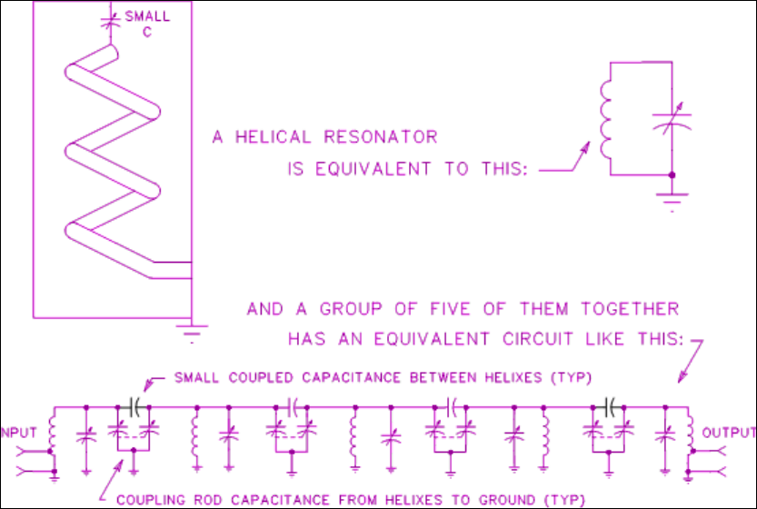
3.1 HELICAL RESONATOR BANDPASS FILTER
LARCAN bandpass filter implementations generally consist of a cascaded series of coupled resonators. Some use
helical resonators; essentially a self supporting high Q coil (the helix) mounted inside a metallic shield enclosure. One
end of the coil is solidly connected to the shield enclosure and the other end is open circuited except for a small
trimmer capacitance to ground. The dimensions of the coil are critical to the frequency of operation; the assembly
behaves as though it were a quarter wave coaxial transmission line resonator. Several sizes of coils and enclosures
are necessary to cover the desired frequency ranges.
Figure 4 indicates the generic assembly of a coupled helical resonator bandpass filter.
The referenced drawing in Figure 4 is a low band filter. The high band unit is laid out identically and appears almost the
same, except the high band helixes have fewer turns of coarser winding pitch and their shield enclosure dimensions
are somewhat smaller.
The desired response shape is presented as Figure 1 below, and the filter electrical equivalents are presented on the
next page as Figure 2. When we examine the assembly, and take capacitances into account, the equivalent circuit of a
helical resonator becomes simply a parallel resonant LC tank circuit having low (trimmer) capacitance and relatively
high inductance. Adjustment of the trimmer produces a change of capacitance and the trimmer's moveable slug is
shaped to appear as a shorted turn, which alters the inductance of the helix.
Matching from and to 50 ohm transmission lines is accomplished with taps on the input and output helixes.
Coupling between sections is electrically a bridged T network of capacitors and is made up of the small capacitance
between the free ends of the coils, controllable by the amount of capacitance to ground that is introduced by the
coupling adjustment screws; the coupling is maximum when the screws are backed out fully from the enclosure.
Shielding partitions placed inside the enclosure between helixes, produce fixed area apertures which affect the
coupling capacitance between helixes. Helix #3 in the Figure 4 drawing has taller partitions on both sides of it, giving
lower capacitance and less coupling than the others.
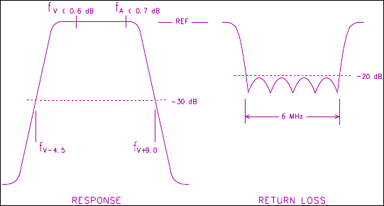
For system use, the tuning and coupling is adjusted for a flat topped response with steep sides, and the desired shape
is such that fV - 4.5 MHz and fV + 9.0 MHz are both 30 dB down, but the carriers must be fV < 0.6 dB and fA < 0.7 dB
departure from flatness. Input and output return loss must be 20dB or better over the full 6 MHz bandwidth. These
sweep curves are shown below as Figure 1.
Figure 1 Bandpass Filter Response
There are nine screw adjustments and two I/O matching (with soldering iron) adjustments that need to be made
simultaneously, and all of them interact with each other. To make these adjustments properly, a network analyzer is
mandatory, and because this is an expensive piece of test equipment not likely to be available in the field, for this
reason we say the unit is not user-adjustable.
Our recommendation is to not adjust the filters at all.
TSM 20-399 Rev 0, Feb 2014 9 10W VHF Amplifier
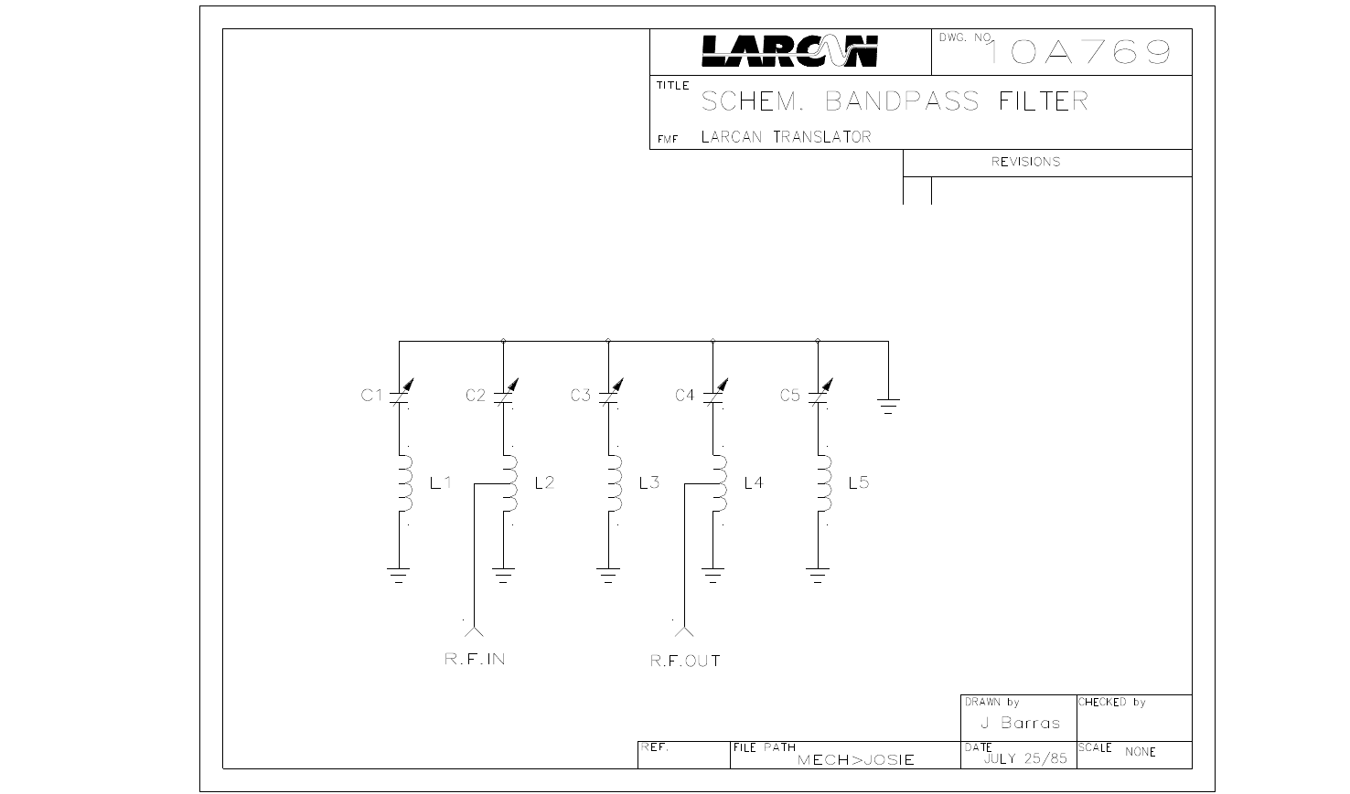
Figure 2 Bandpass Filter Schematic
This is the electrical equivalent of a series of five coupled helical resonators. Similar lower power filters are built using
conventional air wound coils and ceramic trimmer capacitors, and these will be described next.
3.2 LOW POWER FILTER FOR HIGH BAND
The configuration of this filter is similar to the previously described helical resonator type in that it uses five LC
resonant circuits, but it differs in that two of these resonant circuits behave as high Q traps for frequencies outside the
band edge (–4.5 and +9 MHz). The overall response has a reasonably flat top and steep sides. Factory adjustment is
made to achieve the same in-band response (carriers must be fV < 0.6 dB and fA < 0.7 dB departure from flatness) as
described for the helical resonator filter. (We would have preferred to use this 20B704G1 filter for the 50 watt high
band system as well, except that the ceramic trimmers overheated due to the higher RF currents at the 50 watt level,
so the decision was made to go with the higher power helical resonator filter for 50 watt high band transmitters).
Like the helical resonator filter, there are nine screw adjustments and two I/O matching (with soldering iron)
adjustments that need to be made simultaneously, and all of them are interactive. Accurate adjustment is impossible
without the aid of a network analyzer, and because of the expense of this gear it is not as likely to be available in the
field; for this reason we say the filter is not user-adjustable.
It is possible to use a sweep generator and detector for setting the response of either filter, but unless an accurate 50
ohm return loss bridge is used with the sweep generator, there is no way to properly set up the input and output
matching.
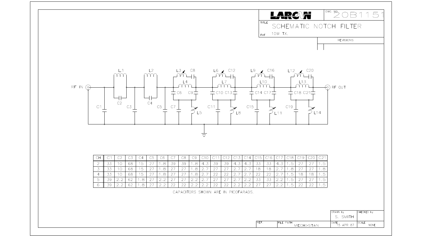
3.3 LOW PASS AND NOTCH FILTER FOR LOW BAND
Ten adjustable inductors, four fixed inductors (which also can be adjusted slightly by spreading their turns with a
suitable tool), and twenty-one fixed capacitors, make up the complete filter. Functionally, it consists of two sections of
shunt m-derived low pass network, followed by four bridged-tee notch networks. Its signal direction is intended to be
TSM 20-399 Rev 0, Feb 2014 10 10W VHF Amplifier
one way only, as indicated in Figure 6.
The low pass section (L1, L2, C1 through C5) of the filter is designed to cut off at a frequency lower than the second
harmonic, so that only the fundamental is able to pass through, but harmonics are blocked.
The four notch sections are tuned to reject fV–9, fV–4.5, fV+9, and fV+13.5 MHz (down typically 18, 30, 24, and 26dB
respectively - sometimes one of the tuned circuits at fV–9, either L3 or L5, is readjusted to fV–4.5 in order to make that
notch deep enough that the fV–3.58 MHz component is sufficiently attenuated).
L4, L7, L10, and L13 are adjusted to set the width and depth of the notch. A typical network analyzer transfer function
plot of the filter indicates the four notches at the values stated above, and the band pass of the fV and fA frequencies
and the channel between, having less than 0.1dB of ripple.
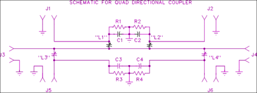
3.4 RF DIRECTIONAL COUPLER
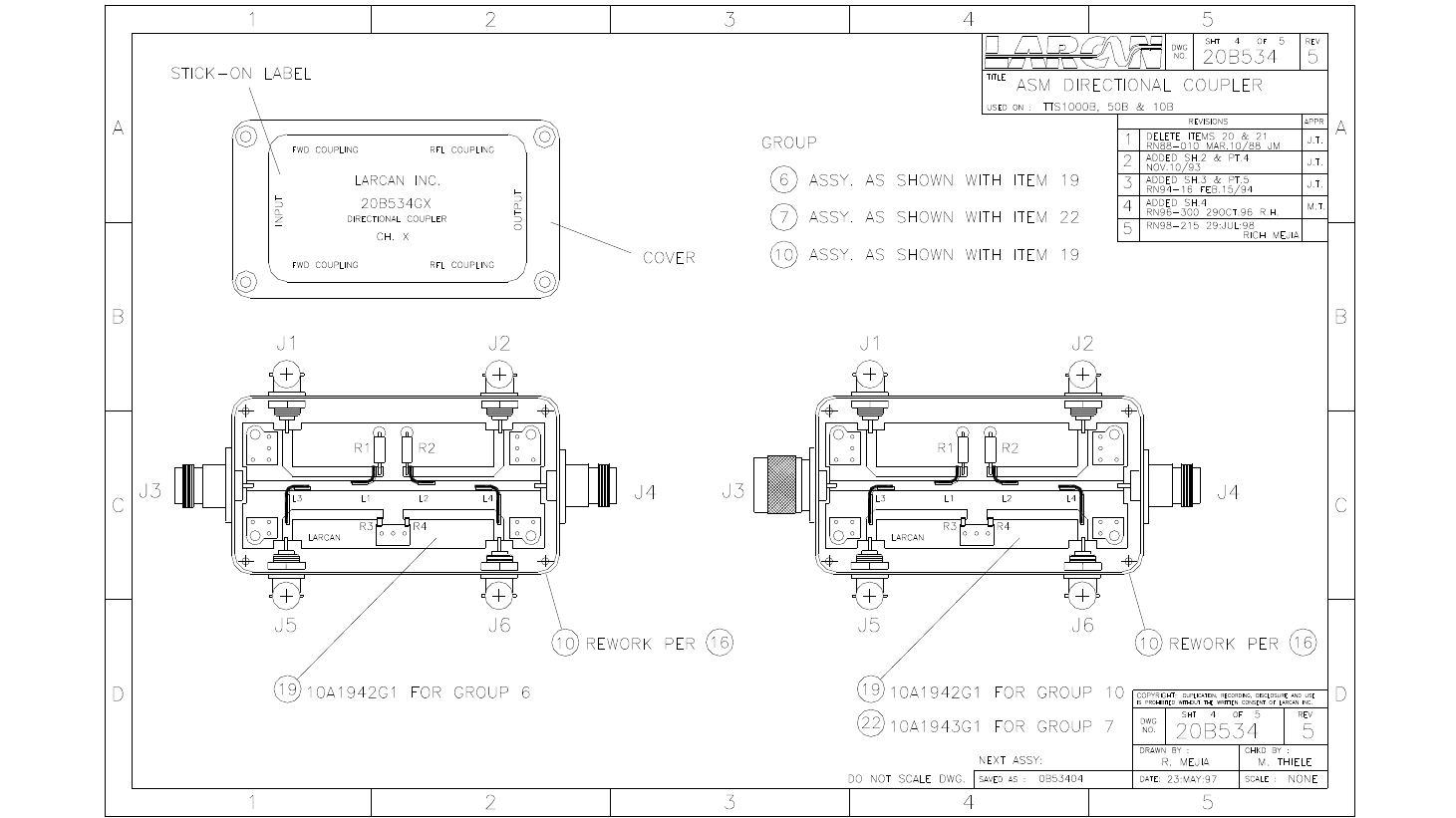
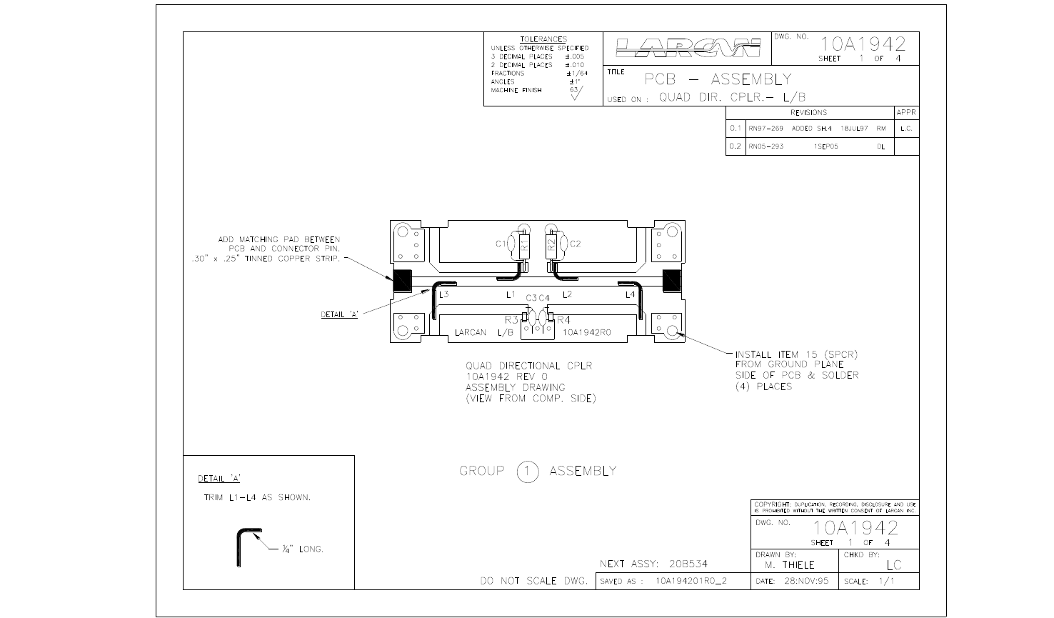
A directional coupler is based on the principles of inductive (magnetic) coupling and capacitive coupling.
In the LARCAN quad directional coupler implementation as shown in Figure 3 (schematic equivalent), the RF to be
sampled passes through a microstrip transmission line that is connected between the transmitter output filter at J3 and
the antenna system at J4. The magnetic field surrounding the hot conductor of this transmission line induces a small
RF current flow in other conductors situated parallel to it. One end of each sampling conductor is terminated by a
resistor to ground. Sometimes small capacitors are connected across these resistors to provide a termination that
remains resistive over the band. The other end of each sampling conductor connects to an external load, usually a 50Ω
input of something such as an RF detector for AGC, the station demodulator, or an RF detector for VSWR sensing.
If the sampling system as described in the forgoing paragraph were dependent only on magnetic coupling and
absolutely no capacitance were present, the external loads would be driven with RF samples regardless of the
direction they came from. Our objective is that the system should be directional. A signal coming from the transmitter
should be seen by the "forward" ports, and a signal reflected back from the antenna should be seen by the "reflected"
ports. At the same time, as little as possible of the forward signal from the transmitter should be seen on these
reflected ports.
The desired directivity is achieved by the capacitance between the main line and each sampling line. The presence of
this capacitance changes the relative phase of the RF signal seen in the sampling line such that the capacitively
coupled signal adds to the inductively coupled signal at the end of the line nearest the signal source, and subtracts
from it at the other end, thus the sample becomes directive.
This capacitance is trimmed by small "gimmick" capacitors designated L1 throughL4. They are short pieces of Teflon
sleeved magnet wire which possess a fraction of a nanohenry of inductance and are mainly small capacitors. They are
factory adjusted by bending the wire to control the amount of coupling capacitance between the transmission line and
the sampling loop concerned. The position of the capacitor along the loop does not seem to matter.
Terminations are provided at the subtractive ends of each of the four sampling lines.
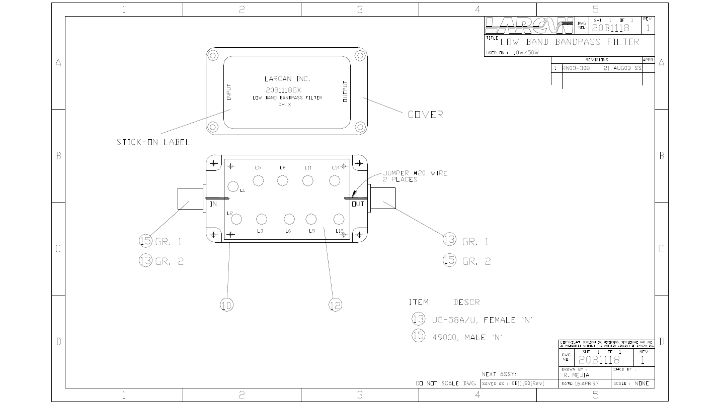
In the enclosure shown in Figure 4, J3 and J4 are the filter and antenna ports respectively, and J1, J5 are "forward"
samples which are maximum amplitude for signals incident on J3; while J2, J6 are "reflected" samples which are
maximum amplitude for signals incident on J4.
Different coupling values are obtained from the spacing of conductors; the nearer the spacing, the greater the coupling.
Coupling is also greater according to frequency, and rises at a rate of about 6dB per octave. In the boards shown in
Figure 4, the J1 and J2 signals will be about 10dB greater amplitude (about 36dB below the generator level at 70MHz
on low band or 200MHz on high band) than the signals sampled from J5 and J6 (about -46dB). Generally for system
purposes the reflected signal sample to the VSWR supervisory system should be taken from the J2 connector
because it has greater coupling and we need to measure a much smaller signal in a detector having finite small-signal
sensitivity. System forward signals can be taken from J1 for the AGC detector, and J5 for the system monitoring
demodulator.
A network analyzer and extremely accurate terminations are required for setting up the directional coupler. The
adjustments are made to the trimming capacitances "L1" through "L4", and the capacitors in parallel with resistors R1
TSM 20-399 Rev 0, Feb 2014 11 10W VHF Amplifier
through R4. Our target is directivity of 30dB or better on each sampling port, and coupling (forward direction) for J1 and
J2 about 36dB down, J5 and J6 about 46dB down.
No user adjustments are possible nor recommended. Very little can go wrong with the directional coupler other than
from the antenna being hit by lightning, and inspection is all that is recommended.
Figure 3 RF Directional Coupler Schematic
TSM 20-399 Rev 0, Feb 2014 12 10W VHF Amplifier
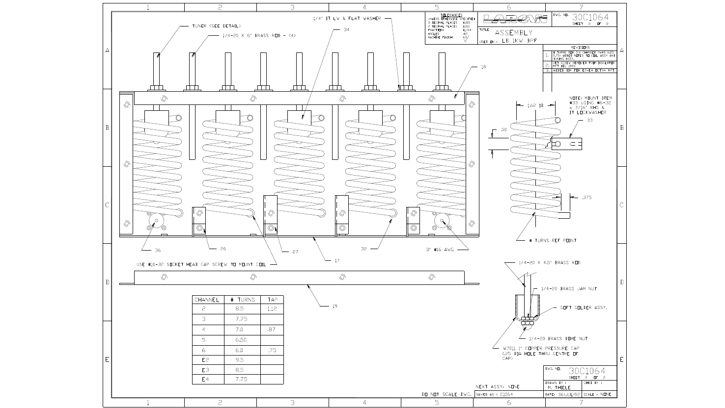
Figure 4 Generic Helical Resonator Bandpass Filter Assembly
TSM 20-399 Rev 0, Feb 2014 13 10W VHF Amplifier
Figure 5: Filter Schematic
TSM 20-399 Rev 0, Feb 2014 14 10W VHF Amplifier
Figure 6 Low Band Bandpass and Notch Filter Assembly
TSM 20-399 Rev 0, Feb 2014 15 10W VHF Amplifier
Figure 7 Low Band Bandpass and Notch Filter Schematic
TSM 20-399 Rev 0, Feb 2014 16 10W VHF Amplifier
Figure 8 RF Directional Coupler
TSM 20-399 Rev 0, Feb 2014 17 10W VHF Amplifier
Figure 9 Low Band Coupler PC Board Assembly
TSM 20-399 Rev 0, Feb 2014 18 10W VHF Amplifier
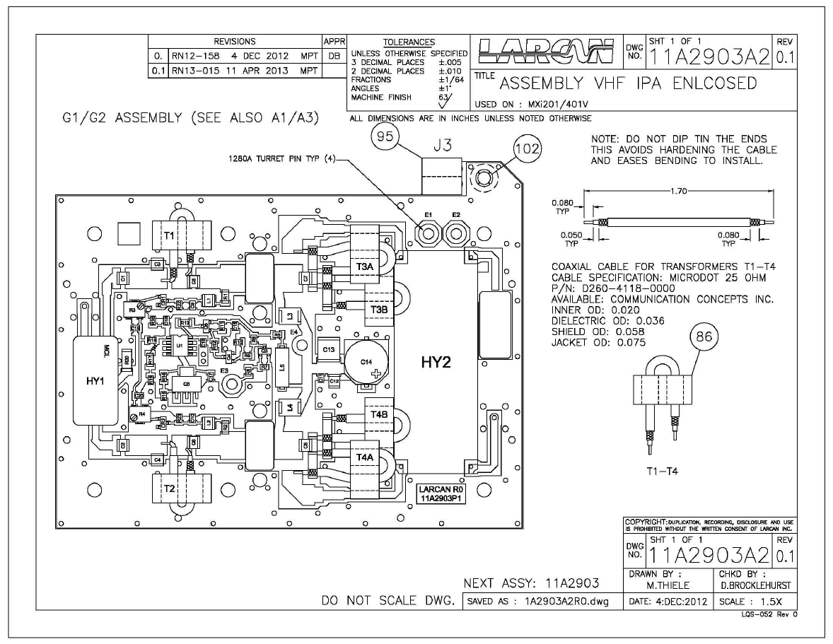
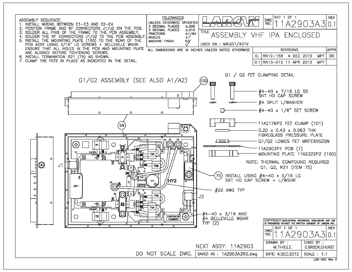
4 RF POWER AMPLIFIER AND HEATSINK ASSEMBLY
The complete RF amplifier chain consists of a preamplifier and a final output amplifier mounted on a convection-
cooled heatsink on the front panel of the unit.A thermal cutout switch removes the power to the drive stages
should the temperature of the heatsink exceed a safe operating level.
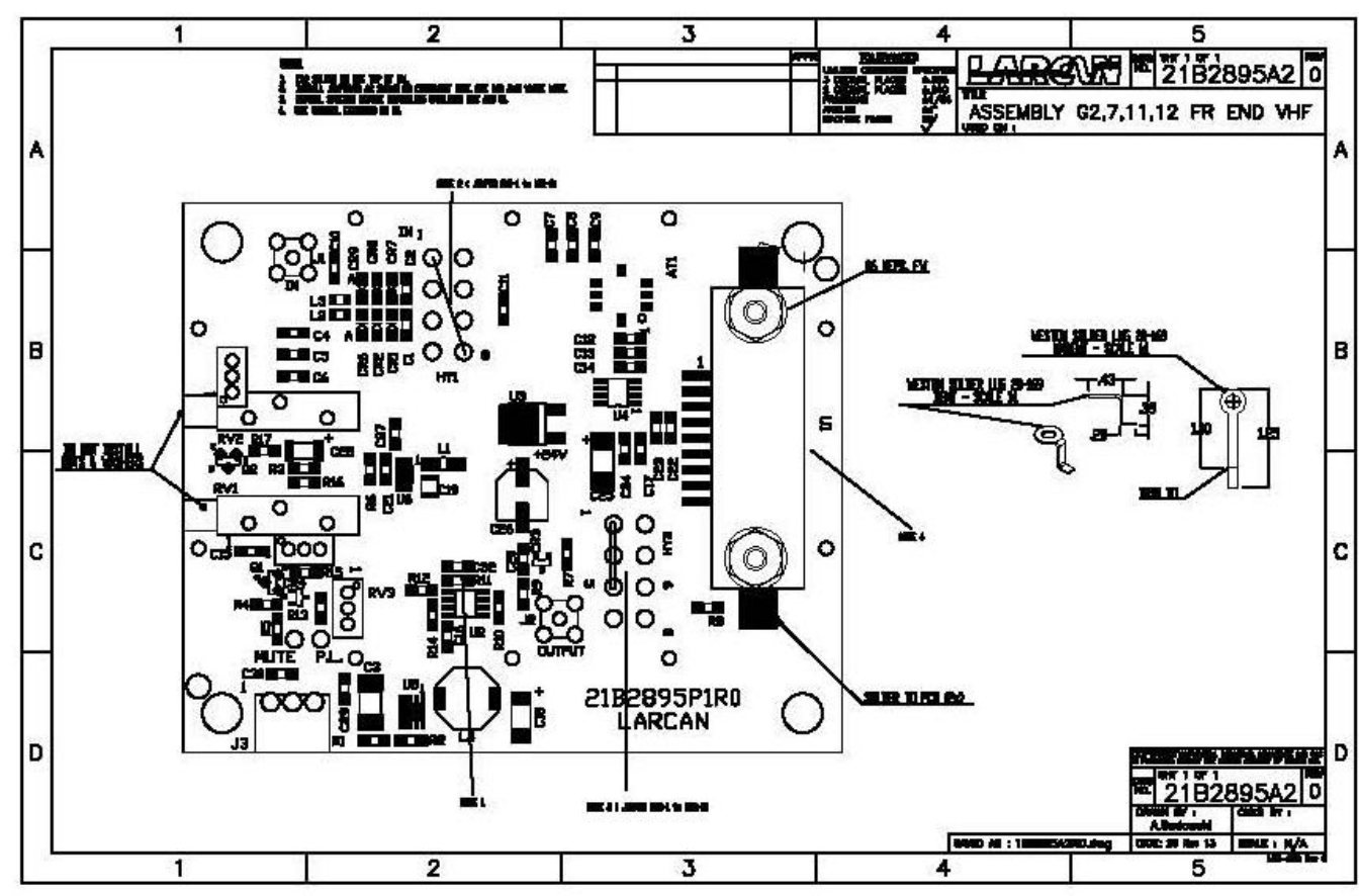
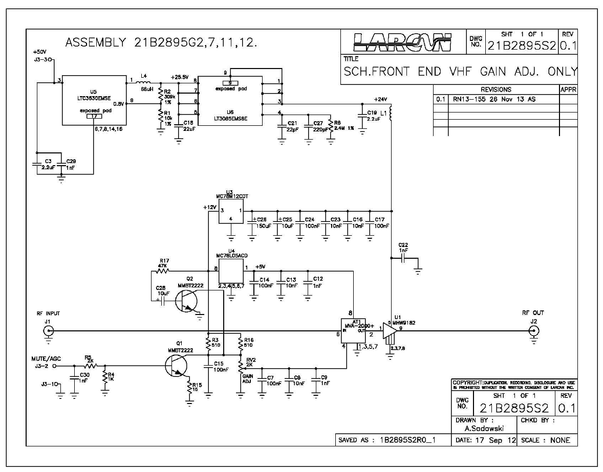
4.1 PREAMPLIFIER
The preamplifier stage consists of a gain-block hybrid amplifier. This simple board has a regulator circuit to supply
the hybrid as well as a PIN attenuator module which is controlled by the VSWR limiter circuitry on the
detector/metering board. Refer to figures 10 and 11. This board has no user adjustments and is broadband,
covering both VHF high and low band.
4.2 OUTPUT AMPLIFIER
The output amplifier is a dual amplifier with FET transistors in quadrature parallel operation. The input signal is
split via hybrid 3dB coupler, and the output from each transistor amplifier is recombined with a similar (higher
power handling) 3dB hybrid. These hybrid couplers are the only components that differ between the Band I and
the Band III amplifiers.
A matching network consisting of a combination of circuit traces and impedances, lumped components and
transmission line transformers converts the input 50 ohm to the low impedance required at the input of the FET. A
similar matching network is used to match the output impedance of the FET to the required 50 ohms. There are
no tuneable circuits in these matching networks.
A thermally compensated biasing network is provided to maintain constant idle current throughout the amplifiers
operating temperature range. The bias adjustments are provided by R3 and R4. Should there be a device failure,
only the bias current should be re-verified upon replacement of the FET. Note – the circuit has a bias shutdown
feature which is not used in this application. Refer to figures 12 through 14
TSM 20-399 Rev 0, Feb 2014 19 10W VHF Amplifier
Figure 10: Preamplifier Assembly
TSM 20-399 Rev 0, Feb 2014 20 10W VHF Amplifier
Figure 11: Preamplifier Schematic
TSM 20-399 Rev 0, Feb 2014 21 10W VHF Amplifier
Figure 12: Final Amplifier Assembly (sht 1)
TSM 20-399 Rev 0, Feb 2014 22 10W VHF Amplifier
Figure 13: Final Amplifier Assembly (sht 2)
TSM 20-399 Rev 0, Feb 2014 23 10W VHF Amplifier
Figure 14: Final Amplifier Schematic
TSM 20-399 Rev 0, Feb 2014 24 10W VHF Amplifier
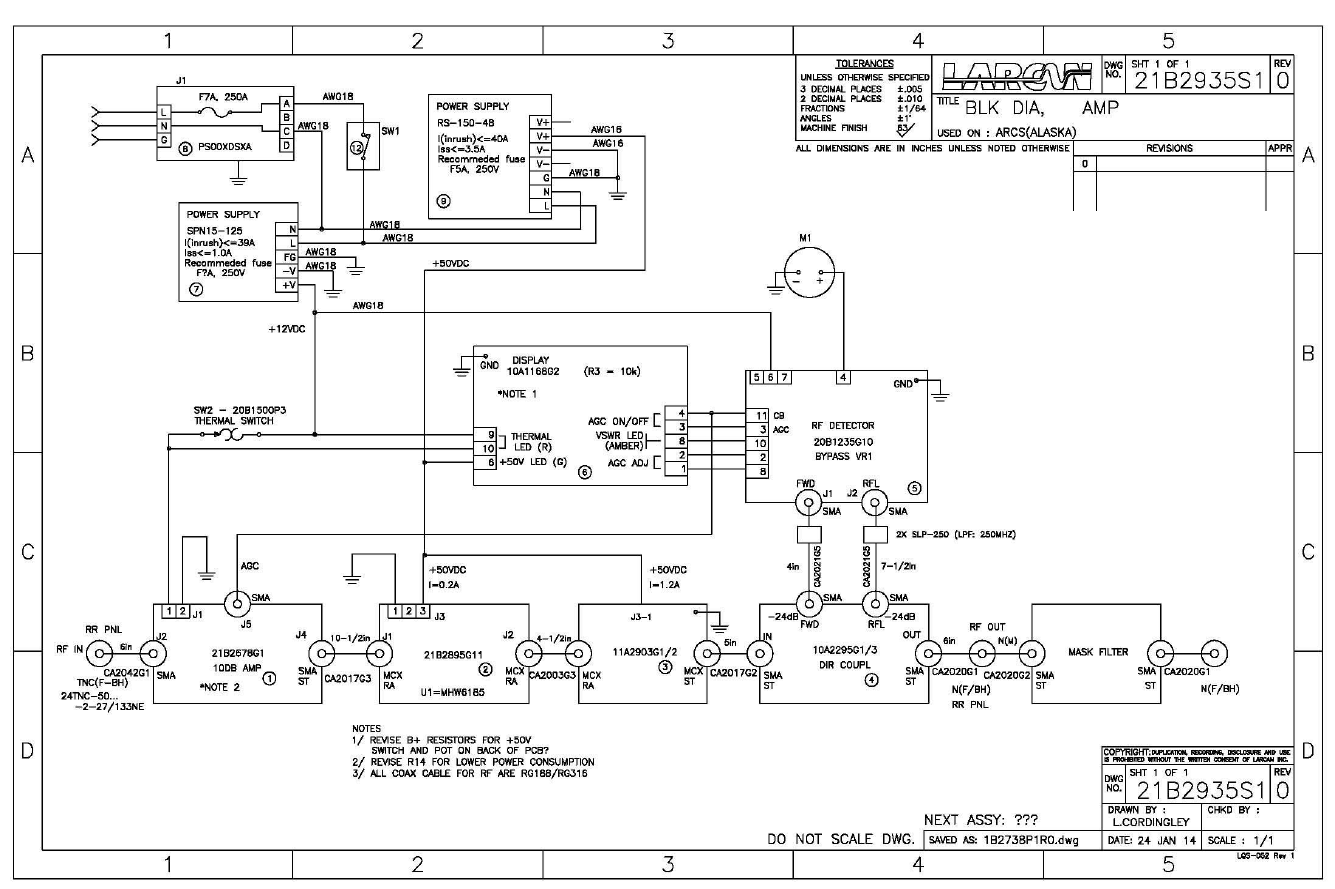
5 METERING AND CONTROL
5.1 SYSTEM
The Amplifier unit is very straightforward in operation. A front panel switch is provided to turn on and off the 48V (also
herein referred to as 50V) power supply. Voltage is applied to the amplifier and preamp, and via a thermal switch to a
small gain stage. The output samples of forward and reflected power are fed to the RF Detector circuit which feeds
the output power meter and also provides a protection and monitoring circuit in case of VSWR. Only the cutback
function from this protection circuit is utilized, feeding a cutback voltage to the drive stages to reduce the output power
to a safe level. Once the VSWR problem is removed and the load is acceptable, the drive power will be once again
increased to normal level.
Indicators are provided on the front panel to indicate that power supplies are turned on, VSWR cutback is occurring,
and if the thermal cutout has opened. Refer to figure 15
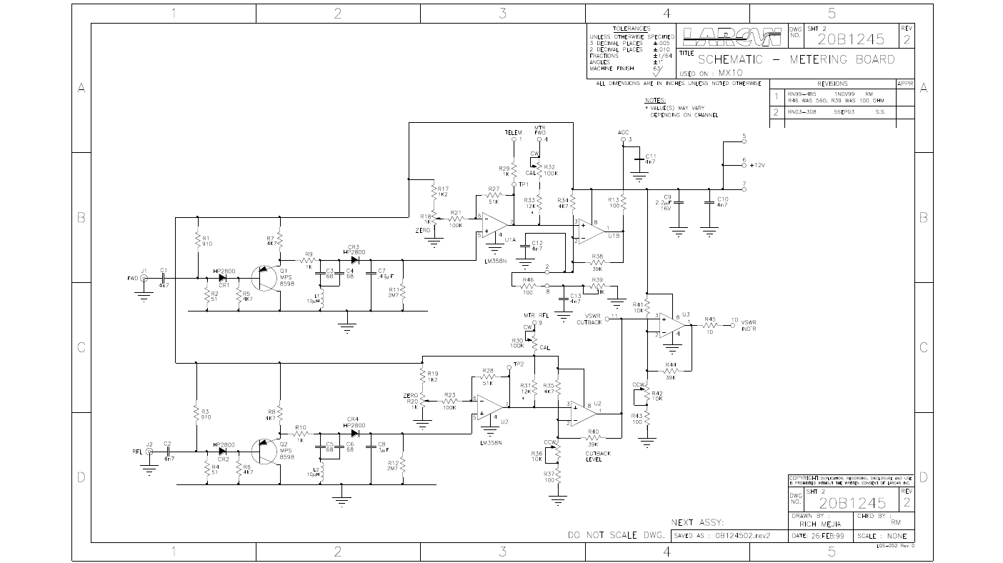
5.2 RF DETECTORS
The #1 Forward (#2 Reflected) RF power sample is applied to J1 (J2) and is terminated by R2 (R4). A small amount of
forward bias is applied to CR1 (CR2) via R1 and R5 (R3, R6) to overcome the threshold voltage of the diode and
enhance its detection linearity at low signal levels. The opposing connection of CR1 (CR2) diode junction and Q1 (Q2)
emitter-base junction provides temperature compensation.
CR3 (CR4) is a detector with a time constant set by C7 and R11 (C8, R12). The signal from this peak detector is fed to
op-amp U1 (U2) pin 5. The gain of this stage is 0.5x (0.5x), and its output on pin 7 feeds the meter, which is located on
the front panel of the amplifier.
U1 (U2) output pin 7 zero-offset voltage is controlled by R18 (R20). This pot should be set with no RF input, while you
watch the voltage on TP1 (TP2) you are setting the pot and you will observe the decrease of the voltage towards zero.
When the voltage stops decreasing, stop your adjustments as well. Expect about 50mV offset voltage when the
op-amp output is almost touching ground. If the pot is turned beyond this point, the output stage of the op-amp will be
driven into saturation and be unable to respond to low power levels.
The output of U1-7 (U2-7) drives the RF power meter through R32 (R30) which set the meter deflection with a known
RF signal. U1-7 (U2-7) drives. Forward calibration is done with full rated power and a forward RF sample from the
directional coupler applied to J1. R32 is adjusted for a 100% reading on the forward power meter position.
For Reflected calibration, the same forward RF sample is then applied to J2, R30 is set for a 100% reading on the
Reflected Power meter. Refer to figures 16 and 17.
5.3 RF METERING BOARD CALIBRATION
5.3.1 Forward Power Meter Calibration - Zero Adjust
With no RF input connected, measure the DC voltage at U1-7 (or TP1) and adjust R18 until the output voltage at U1-7
(TP1) drops to a minimum, approximately 10 to 50mVDC. A DC coupled scope will make the adjustment easier to see.
The objective is to place the U1 output as near the op-amp ground rail as possible without the op-amp going into
saturation. Turning the pot farther will decrease the sensitivity of the system for small signals. Once this minimum
voltage has been reached, do not re-adjust R18.
5.3.2 Reflected Power Meter Calibration - Zero Adjust
With no RF input connected, measure the DC voltage at U2-7 (or TP2) and adjust R20 for a minimum, which should
be approximately 50 mVDC. Once this minimum voltage has been reached, do not re-adjust R20. This adjustment is
done in precisely the same way as in step above.
TSM 20-399 Rev 0, Feb 2014 25 10W VHF Amplifier
5.3.3 Forward Power Calibration
Set the exciter RF output for the transmitter to run at its operating power. Adjust R32 for a forward power meter
reading of 100%.
NOTE: Before proceeding to the next step, ensure that the Pin Attenuator Board has been setup according to the
procedure on the Pin Attenuator Board section of this manual.
5.3.4 Reflected Power Calibration
1. Temporarily defeat the VSWR cutback protection (if it has been initially setup) by adjusting R36 fully clockwise
(CW). With the transmitter still at "full power”, disconnect the RF input cable from J1 and connect it instead to the
reflected power input J2. Switch to position „RFL‟ and adjust R30 so that the reflected power reads 100. This now
corresponds to a reflected power of 100%.
2. Enable the VSWR cutback by turning R36 counter clockwise until the meter indicates 10% output. This means that
in severe VSWR conditions such as in an open circuit, the amplifier will automatically cut back to 10% in order to
protect itself.
3. Replace the cables in their proper connections. RFL meter reading should be zero and the FWD meter reading
should be back to 100%. If the FWD reading is much less than 100%, R36 was probably over adjusted.
TSM 20-399 Rev 0, Feb 2014 26 10W VHF Amplifier
Figure 15: System Block Diagram
TSM 20-399 Rev 0, Feb 2014 27 10W VHF Amplifier
Figure 16:Metering Board Assembly
TSM 20-399 Rev 0, Feb 2014 28 10W VHF Amplifier
Figure 17: Metering Board Schematic
TSM 20-399 Rev 0 Feb. 2014 10W VHF Amplifier