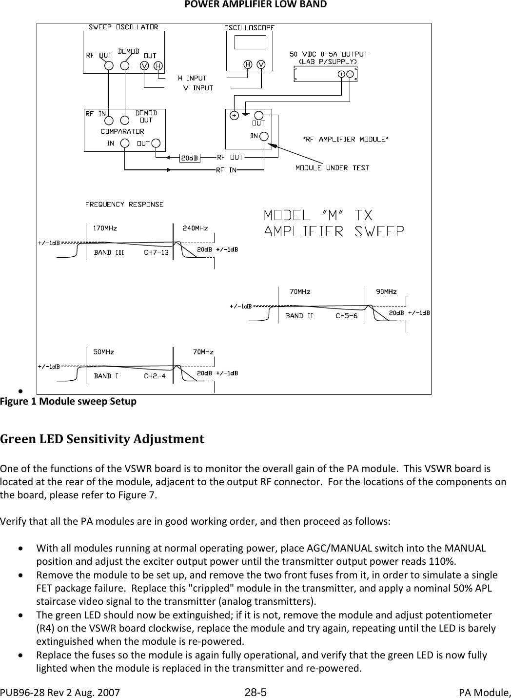
Larcan DTT250M Digital Television Broadcast Translator User Manual
Larcan Inc Digital Television Broadcast Translator Users Manual
UserManual.wiki
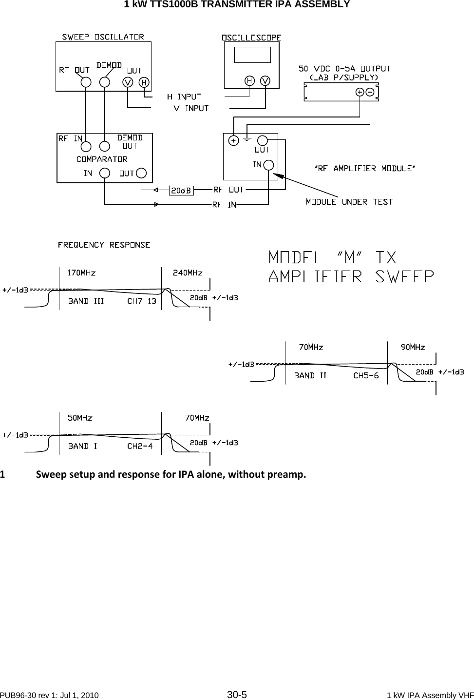
>
Larcan
>
DTT250M User Manual
Users Manual
Navigation menu
Upload a User Manual
Namespaces
Wiki Guide
HTML
PDF
Info
Views
User Manual
Discussion / Help
Navigation