Larcan DTT250M Digital Television Broadcast Translator User Manual
Larcan Inc Digital Television Broadcast Translator Users Manual
Larcan >
Users Manual
GENERAL DESCRIPTION
TSM 20-275D rev 0: Jul 1, 2010 1 DTT250M
DTT250M
–
250W Di
g
ital Television Transmitte
r
INTRODUCTION
ThismanualdescribestheLARCANmodelDTT250MVHFDigitalTelevisionTransmitter.
LARCANall‐solid‐state250WVHFtransmittersaredesignedtooperateconservativelyat250Waverage
DTVpowerwithsuperbperformance,reliabilityandoperatingeconomy.
Thetransmitterandexciterortranslatorchassisarepackagedinasingle19"cabinet.Thesimplicityof
design,thedeploymentofallmodularandothersubassemblies,andtheuseofstandardreadily
availablecomponents,enhancesserviceability.
Importanttransmitterparametersaremonitored,andcanbedisplayedonthemeterbuiltintothe
amplifier.Additionally,allmeterreadingsaremadeavailableasDCsignalsfortelemetrybyremote
controlsystems.TheDTT250M,likeallotherLARCANtransmittingequipment,issuitablefor
automaticorremote‐controloperation.
AMPLIFIERCHAIN
TheRFoutputoftheexciterisfedtoaconservativelydesignedbroadbandsolid‐stateamplifier.This
amplifierrequiresnotuningoradjustmentwithinitsbandofoperation.Simplicityofoperation,
reducedmaintenancecostsandincreasedreliabilityareafewofthemajorbenefitsderivedfromthis
modularamplifier.Thismoduleisoperatedwellbelowitsmaximumratings.
Theamplifierchainconsistsofthreestagesofamplification.
Thepreamplifierstageisahighgain,broadband,thin‐filmintegratedcircuitamplifieroperatingclassA.
TheIPAstageconsistsofapairofpush‐pullFETsinasinglecase,operatinginclassABasalinear
amplifier.ThisamplifierusestheidenticaldualFETdevicethatisusedbythePAmodule.
Thefinalamplifierstageconsistsofsixpush‐pullFETamplifiersthatoperateinclassAB,inthreegroups
oftwoinquadrature,andarecombinedinquadratureandthenina3‐waycombiner.Theamplifier
moduleisratedfor250wattsaverageATSCoutput.Themoduleisprovidedwithsoft‐start,VSWR
protection,andamonitorport.
Theamplifieroutputisfedtothebandpassfilterandthedirectionalcoupler,whichprovidesasmall
sampleofforwardandreflectedoutputpowerforAGCandVSWRsupervisoryfunctions.The
transmitteroutputthenpassestotheantennasystem.
GENERAL DESCRIPTION
TSM 20-275D rev 0: Jul 1, 2010 2 DTT250M
DTT250M
–
250W Di
g
ital Television Transmitte
r
TRANSMITTERCONTROL
Thecontrolcircuitryinthissolidstatetransmitterissimple.Interlockingconsistsoftheenabling
circuitrynecessarytoensurethatanyexternalpatchpanellinkoperation,orRFswitching,canonlybe
donewithRFturnedoff.
nableJ5‐5.
Allcontrolwiringofthetransmitterpassesthroughacontrolcircuitboard(prefix5B),andfacilitiesare
providedonthisboardfortelemetry,status,andcontrolconnectionstoandfromaremotecontrol
system.Theseareavailableon15contactD‐shellconnectorJ5.
Forlocaloperation,simplyplacetheLOC‐REMswitchintheLOCposition.Forremotecontrol
operationtheLOC‐REMswitchmustbeintheREMposition.Thisplaces+12VonRemoteE
TheRemoteEnable+12VappearsasanarmingsignalatJ5‐5,andthemomentaryconnectionofthis
+12VtoJ5‐13turnsthetransmitterON,andmomentaryconnectionofthe+12VtoJ5‐8turnsthe
transmitterOFF.
ThetransmittercontrolandinterlockwiringisalsobroughtoutonJ3,whichisprovidedwithaterminal
blockstyleofconnectorinterface.RemoteEnable,RemoteOn,RemoteOff,andExternalInterlocks1
and2areallbroughtoutonJ3forconnectionasrequired.
AthermostatisprovidedinthePAheatsinktoopentheinterlockchainshouldanunlikelyoverheating
conditionoccur.
CONTENTS
1BANDPASS FILTER ........................................................................................................................................................ 2
2RF DIRECTIONAL COUPLER ...................................................................................................................................... 4
PUB96-26 Rev 1 September 13, 2005 26-1 RF Output: BP Filter & Directional Coupler
1 BANDPASS FILTER
Drawing References: Figure 1 and Figure 4.
The LARCAN bandpass filter implementation consists of a cascaded series of coupled helical resonators. A
helical resonator is essentially a self supporting high Q coil (the helix) mounted inside a metallic shield enclosure.
One end of the coil is solidly connected to the shield enclosure and the other end is open circuited except for a
small trimmer capacitance to ground. The dimensions of the coil are critical as to frequency of operation; the
assembly behaves as though it were a quarter wave coaxial transmission line resonator. Several sizes of coils
and enclosures are necessary to cover the desired frequency ranges. Figure 4 indicates the generic assembly of
a coupled helical resonator bandpass filter.
The referenced drawing in Figure 4 is a low band filter, but the high band unit is laid out identically and appears
almost the same, except the high band helixes have fewer turns of coarser winding pitch, and their shield
enclosure dimensions are somewhat smaller.
The desired response shape is presented as Figure 1, and the filter electrical equivalents are presented as Figure
2. When we examine the assembly, and take capacitances into account, the equivalent circuit of a helical
resonator becomes simply a parallel resonant LC tank circuit having low (trimmer) capacitance and relatively high
inductance. Adjustment of the trimmer produces a change of capacitance, and the trimmer's moveable slug is
shaped to appear as a shorted turn, which alters the inductance of the helix.
Matching from and to 50 ohm transmission lines is accomplished with taps on the input and output helixes.
Coupling between sections is electrically a bridged T network of capacitors, and is made up of the small
capacitance between the free ends of the coils, controllable by the amount of capacitance to ground that is
introduced by the coupling adjustment screws; the coupling is maximum when the screws are backed out fully
from the enclosure. Shielding partitions placed inside the enclosure between helixes, produce fixed area
apertures which affect the coupling capacitance between helixes. Helix #3 in Figure 4 has taller partitions on both
sides of it, giving lower capacitance and less coupling than the others.
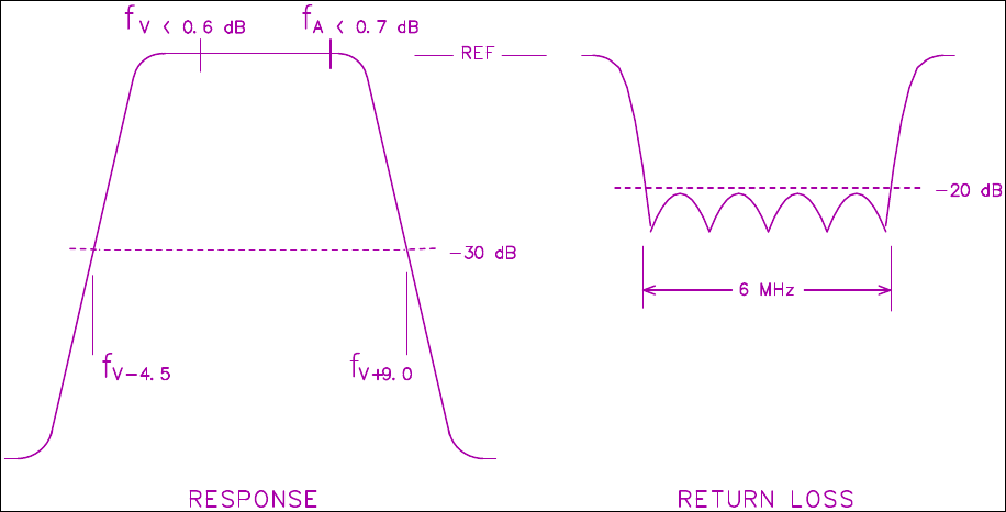
For system use, the tuning and coupling is adjusted for a flat topped response with steep sides, and the desired
shape is such that fV - 4.5 MHz and fV + 9.0 MHz are both 30 dB down, but the carriers must be fV < 0.6 dB and
fA < 0.7 dB departure from flatness. Input and output return loss must be 20 dB or better over the full 6 MHz
bandwidth. These sweep curves are shown below as Figure 1A.
There are nine screw adjustments and two I/O matching (with soldering iron) adjustments that need to be made
simultaneously. Factory adjustment is never attempted without the aid of a network analyzer, and for this reason
we say the unit is not user-adjustable.
PUB96-26 Rev 1 September 13, 2005 26-2 RF Output: BP Filter & Directional Coupler
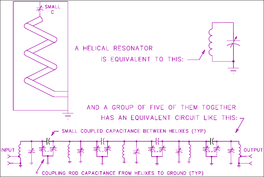
Figure 1 5-Pole Bandpass Filter Curves
Figure 2 5-Pole Bandpass Filter Used in the TTS1000B
PUB96-26 Rev 1 September 13, 2005 26-3 RF Output: BP Filter & Directional Coupler
2 RF DIRECTIONAL COUPLER
A directional coupler is based on the principles of inductive (magnetic) coupling and capacitive coupling.
In the LARCAN quad directional coupler implementation as shown in Figure 3 (schematic equivalent) and Figure
5 (assembly), the RF to be sampled passes through a microstrip transmission line that is connected between the
transmitter output filter at J3 and the antenna system at J4. The magnetic field surrounding the hot conductor of
this transmission line induces a small RF current flow in other conductors situated parallel to it. One end of each
sampling conductor is terminated by a resistor to ground. Sometimes small capacitors are connected across
these resistors to provide a termination that remains resistive over the band. The other end of each sampling
conductor connects to an external load, usually a 50 Ω input of something such as an RF detector for AGC, the
station demodulator, or an RF detector for VSWR sensing.
If the sampling system as described in the forgoing paragraph were dependent only on magnetic coupling and
absolutely no capacitance were present, the external loads would be driven with RF samples regardless of the
direction they came from. Omnidirectionality is not wanted; our objective is that the system should be directional,
that is, a signal coming from the transmitter should be seen by the "forward" ports, and a signal reflected back
from the antenna should be seen by the "reflected" ports, but at the same time as little as possible of the forward
signal from the transmitter should be seen on these reflected ports.
The desired directivity is achieved by the capacitance between the main line and each sampling line. The
presence of this capacitance changes the relative phase of the RF signal seen in the sampling line such that the
capacitively coupled signal adds to the inductively coupled signal at the end of the line nearest the signal source,
and subtracts from it at the other end, thus the sample becomes directive.
This capacitance is trimmed by small "gimmick" capacitors designated L1 through L4. They are in reality short
pieces of Teflon sleeved magnet wire which, although they may possess a fraction of a nanohenry of inductance,
are mainly small capacitors which are factory adjusted by bending the wire to control the amount of coupling
capacitance between the transmission line and the sampling loop concerned. The position of the capacitor along
the loop does not seem to matter.
Terminations are provided at the subtractive ends of each of the four sampling lines.
In the enclosure shown in Figure 5, J3 and J4 are the filter and antenna ports respectively, and J1, J5 are
"forward" samples which are maximum amplitude for signals incident on J3; while J2, J6 are "reflected" samples
which are maximum amplitude for signals incident on J4.
Different coupling values are obtained from the spacing of conductors; the nearer the spacing, the greater the
coupling. Coupling is also greater according to frequency, and rises at a rate of about 6dB per octave. In the
boards shown in Figure 5, the J1 and J2 signals will be about 10dB greater amplitude (about 36dB below the
generator level at 70 MHz on low band or 200 MHz on high band) than the signals sampled from J5 and J6
(about -46dB). Generally for system purposes the reflected signal sample to the VSWR supervisory system
should be taken from the J2 connector because it has greater coupling and we need to measure a much smaller
signal in a detector having finite small-signal sensitivity. System forward signals can be taken from J1 for the
AGC detector, and J5 for the system monitoring demodulator.
A network analyzer and extremely accurate terminations are required for setting up the directional coupler. The
adjustments are made to the trimming capacitances L1 through L4, and the capacitors in parallel with resistors
R1 through R4. Our target is directivity of 30dB or better on each sampling port, and coupling (forward direction)
for J1 and J2 about 36dB down, J5 and J6 about 46dB down.
No user adjustments are possible or recommended. Very little can go wrong with the directional coupler other
than from the antenna being hit by lightning, and inspection is all that is recommended, nothing more.
PUB96-26 Rev 1 September 13, 2005 26-4 RF Output: BP Filter & Directional Coupler
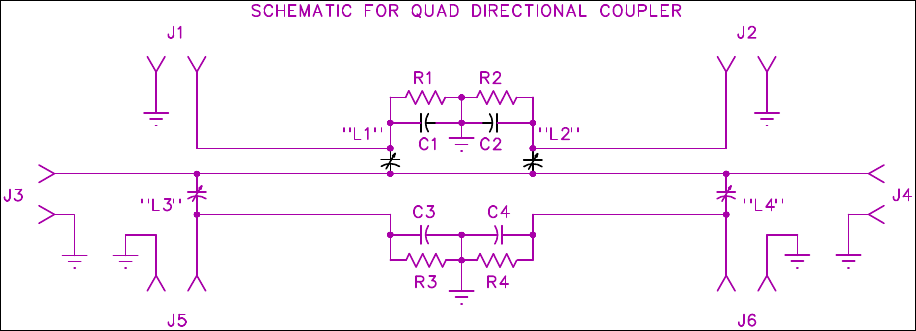
Figure 3 Quad Directional Coupler Equivalent Schematic
PUB96-26 Rev 1 September 13, 2005 26-5 RF Output: BP Filter & Directional Coupler
POWERAMPLIFIERLOWBAND
PUB96‐28Rev2Aug.2007 PAModule,
CONTENTS
FUNCTIONAL DESCRIPTION .....................................................................................................................................1
6-WAY SPLITTER/INPUT BOARD .............................................................................................................................1
FET RF AMPLIFIERS ...............................................................................................................................................1
6-WAY COMBINER/OUTPUT BOARD .......................................................................................................................2
VSWR CONTROL BOARD .......................................................................................................................................2
GREEN LED SENSITIVITY ADJUSTMENT.................................................................................................................5
POWERAMPLIFIERLOWBAND
PUB96‐28Rev2Aug.2007 28-1PAModule,
FunctionalDescription
ThePowerAmplifiermoduleconsistsofasix‐waypowersplitter,sixFETamplifiers,asix‐waypowercombiner,a
VSWRprotectionboard,andpower&I/Oconnectors.Twofull‐sizeheatsinksprovidethecoolingfortheactive
devices.Itisdesignedfor1.5kWsyncpeakpoweroutputinLowBand54‐88MHzAnalogtelevisionsystems,
andprovidespowergainofapproximately20dB,with1.5kWpeaksyncvisualor900Wauraloutput.The
modulecanprovideupwardsof250Wofaveragedigitalpowerwhenusedwithappropriatepredistortion.Itis
fullyhot‐pluggable,incorporatingprotectivecircuitryforexcessVSWRpowercutback.
6‐WaySplitter/InputBoard
Partnumber:40D1474G1/40D1474G2
References:Figure3andFigure4.
The6‐WaypowersplitterreceivesitsRFinputsignalfromthedrivestageandprovidessixinputsignalsto
integralinputmatchingnetworksforthesixFETamplifiers.Theincomingsignalisfirstsplitinthreebya3‐way
Wilkinsonsplitter,andthethreeresultantsignalsaresplitagainbythree2‐wayWilkinsonsplitterstoprovide
thesixoutputsrequired.Terminationsforthe3‐waysplitterareprovidedbyR109,R110,andR111,with
reactivetrimmingbyL109,L110,andL111;andforthetwo‐waysplitters,terminationsareR101,R103andR105,
withreactivetrimmingbyC106,C116,andC126.ImpedancematchisprovidedbyC145,C142,C138,C144,
C145,C139,andC140whichmakethepathfromthe50Ωinputtothesixquarter‐wavematchingsections,into
alow‐passπnetwork.C148providesinputmatchingforthetransitionfromtheinputconnectortotheinput
transmissionline.
Abuilt‐indetector(CR102andC147)isfedfromadirectionalcouplerontheinputtransmissionline,toprovidea
sampleoftheinputsignalformodulegainmonitoring.R117andR118terminatethedirectionalcoupler.
FETRFAmplifiers
References:Figure3,Figure4,Figure5,Figure6.
Eachofthesixamplifiersinthemoduleconsistsoftwo,sourcegroundedN‐channel,insulatedgateFieldEffect
Transistors(FETs)packagedinasinglecase,operatingclassABinapush‐pullconfiguration.BecausetheseFETs
are"enhancementmode"devices,theyrequirepositivegate‐to‐sourcebiasvoltageoneachgatetocause
source‐drainconduction.AquiescentClassABidlingbiascurrentissetindependentlyforeachhalf.Thegate
voltagerequiredtoproducethisidlingcurrentmayvarybetween2Vand5Vaccordingtothedevice
specificationsheet,andtheidlingcurrentused.FETgatethresholdvoltagesalsoaretemperaturesensitive,so
thermalcompensationisprovidedbyR9,RT1,andR10,RT2.Biascurrentissetto500mAperhalfofthedevice
foranalogoperationand750mAperhalffordigitaloperation.
Gatebiasissuppliedfromanadjustablevoltagedividerfromthe+39Vregulatedbiasrail.ResistorsR1,R2,R3,
R4providegatebiasforonehalfoftheamplifier;R5,R6,R7,R8providebiasfortheotherhalf.
TheRFinputsignalisappliedtobalunT1toprovidetwosignals180˚out‐of‐phase.Thesesignalsarestepped
downtomatchthelowinputimpedanceoftheFETdevicethroughaπ‐networkconsistingofC1,C2,C3,L1,L2,
C4,andthedeviceCG‐S.Thegateinputimpedanceattheoperatingfrequencyislowcomparedwiththevalues
ofR3andR6,whichhavelittleornoeffectatRF.
POWERAMPLIFIERLOWBAND
PUB96‐28Rev2Aug.2007 28-2PAModule,
R3andR6provideaDCpathforbias,andprovideloadingatlowerfrequencieswheregateimpedanceishigh,in
ordertoassistinmaintainingamplifierstability.ThechoiceofC6andC7values,andtheseriesinductanceof
boardtraces,alsoensureseffectivebypassingatcriticalfrequenciesofinterest.
Theoutputmatchingπ‐network,consistingofinductorsL3thruL8,andcapacitancesC13thruC16,transforms
theverylowoutputimpedanceoftheFET,to12.5Ω.Thetwoantiphaseoutputsignalsarefinallycombinedin
balunT2,L9.JumpersplacedacrosspartsofL7andL8,plusthechangedvaluesofC13,C14,C15andC16,
configuresthesystemforchannels5&6operation.
DCisappliedtotheFETdrainsthroughL3,L4fortheQ1Ahalf,andL5,L6fortheQ1Bhalf.L3andL6areshort
sectionsofmicrostriplinewhichtransformtheimpedancesofL4andL5tohighervaluesasseenbytheFET.RF
andlowerfrequenciesarebypassedwithparalleledC5,C9,C10foronehalfoftheamplifier,andC8,C11,C12
fortheotherhalf.Thesegroupsofcapacitorsareselectedinvalueandfortheirinternalequivalentseries
inductancessothattheywillbeaneffectivebypassatcriticalfrequenciesofinterest,includingvideo,toassistin
maintainingstability.
NotethatfusesareprovidedforthevoltagesuppliedtotheFETdrainconnections.Theintentofthesefusesis
toprotectthesurroundingcircuitryintheeventofadevicefailure.Thenormalfailuremodeofactivedevices
suchastheseisshort‐circuit,andthefusewillblowinthiscase,isolatingthedefectivedevicefromtherestof
themoduleandtransmitterpowersupply,allowingtheremainingdevicestokeepoperatingnormally.Ablown
fusecanserveasavaluabletroubleshootingaid,whentryingtoidentifyfaileddevices.
6‐WayCombiner/OutputBoard
Partnumber:40D1472G1/40D1472G2
References:Figure6andFigure3.
Thesixamplifieroutputsareappliedtothree2‐wayWilkinsoncombinersandphasedelayedtocorrectthe
quadratureconditionimposedbytheinputsplitterboard.ThethreeoutputsoftheseWilkinsoncombinersare
againcombinedbya3‐wayWilkinsoncombinerintoasingle50ohmoutput.TerminationsfortheWilkinson
networksaresimilartothoseprovidedontheInputboarddescribedabove,andconsistofR100,C105,R102,
C115,R104,C125forthe2‐ways;andR106,L106,R107,L107,andR108,L108forthe3‐waycombiner.An
outputmatchingπnetworkisformedbyC131thruC134,C136,C137,andC141,alongwiththeseries
inductanceoftheboardtrace.
AdirectionalcouplerfeedsaBNCconnectoronthemodulefrontpanel,andcanbeusedforoutputmonitoring.
Thebi‐directionalcouplerprovidesDCsamplescorrespondingtobothforwardandreflectedpowertotheVSWR
protectionboardformonitoringmodulegainandVSWRprotection.Terminationsforthesecouplerlinesections
areprovidedbyR113,R114,andR115;theRFsamplesforVSWRmonitoringaredetectedbyCR100,C143,and
R112for"forward"andbyCR101,C146,andR116for"reflected".
VSWRControlBoard
Partnumber:20B1549G1
References:Figure7andFigure8.
TheVSWRcontrolboardperformsanumberoffunctions:itprovidesregulatedbiasvoltagestotheFETpower
amplifierstages,itprovideshot‐plug‐incapabilitytoprotecttheamplifiermodulewhenpluggedintoan
POWERAMPLIFIERLOWBAND
PUB96‐28Rev2Aug.2007 28-3PAModule,
operatingtransmitter,itprovidesprotectiontotheFETsagainstover‐dissipationduetohighVSWR,andit
monitorsthemoduleRFpowergain.
Ifthemoduleispluggedintoapoweredtransmitterusingseveralmodulesrunninginparallel,thepowersupply
connectionsarefirstmadethroughthelongercontactsofthemodule’sDCpowerconnectorandintoVSWR
boardJ1pin8.Thisallowstheelectrolyticbypasscapacitorsofallamplifierstochargethroughcurrentlimiting
resistorR5,preventingoverstressofallamplifierfusesduetochargecurrentofthebypasscapacitors.Whenthe
moduleisfullyseated,thehighcurrentcontactsareconnectedandthemodulecanoperatenormally.
InnormaloperationthepowersupplyentersJ1viapin2,andisregulatedto+39VDCbyseriesresistorR10and
zenerdiodeVR1.RegulatorU1providesconstantB+voltageforop‐ampsU2,U3,U4,andthecomparator
referencevoltages.Whenthemoduleisfirstturnedon(orpluggedin)andU1beginsregulating,thecharging
currentofC7turnsonQ1whichpullsthebiaslinelowforabriefperiodoftime.Thisprovidesaslowstartfor
themoduleafterDCpowerisapplied.
TheoverallRFsystemofthetransmitterprovidesoverallVSWRprotectionviatheexternalRFdetectorboards
discussedinothersectionsofthismanual,butVSWRsensingisalsoprovidedinthemoduleforitsownsafety.
Inthetransmittersutilisingmodulesinparallel,oneormorefailedordisconnectedmodulesorafaultinthe
six‐waycombinerorsubsequent3dBcoupler,maycauseamoduleoutputmismatch.
Tothemodule,anymismatchwhichappearsasreflectedpowerisdetectedandsensedatpin11ofJ1to
comparatorcircuitU2B.
R21setsthelevelatwhichVSWRprotectionbegins.Ifthelevelofdetectedreflectedpoweronpin5ofU2B
exceedsthecontrolvoltagesetonpin6,theoutputonpin7willgohigh.R22,C10,andCR1provideafast
attack,slowreleasecontrolvoltagetoQ2whenahighVSWRconditionsuddenlyoccurs.ThiswillturnonQ2
whichturnsonQ4whichquicklyreducesthebiasappliedtothepoweramplifierFETs;thisreducedbiasalso
reducestheirgainandthereforetheirRFoutputandkeepstheamplifieratsafelevels.
Whenamoduleispluggedintoanoperatingtransmitter,theslowstartcircuitryconsistingofC7andQ1will
initiallykeepthemoduleturnedoff.Powerfromtheothermodulesworkingintothecombinerwillenterthe
moduleandbedetectedbythereflectedpowerdetector.Thiswouldpreventthemodulefromeveroperating
properly,unlesstheVSWRcircuitismomentarilyover‐ridden.
ThecircuitofU4producesapulseapproximately2secondsafterpowerisappliedtothemodule.Atpower‐up,
pin2ofU4willbepulledhighbyC11.R26chargesthiscapacitor,andwhenthepin2voltagegoesbelowthe
voltageonpin3,theoutputofU4willgohigh.ApulsewhosedurationiscontrolledbyC9andR18willthenbe
appliedtopin3ofU2A.U3Bdetectsthatthemoduleisnotproducingforwardpowerandthatthereverse
powerishigh.UndertheseconditionstheoutputofU2Agoeshigh,turningonQ3,momentarilydisablingVSWR
protection,andallowingthemoduletocomeon.
DCsamplescorrespondingtoforwardpowerintoandoutofthemoduleareappliedtoU3Apins2and3
respectively.Whenpin3voltageishigherthanthatofpin2,correspondingto"RFgainisokay"thecomparator
outputU3Apin1ishigh,causingthegreenLEDonthefrontpanelofthemoduletolight.Thecomparison
threshold(ie.modulegainisok)issetbyadjustmentofR4.
AdjustmentofbiasvoltagetoestablishproperquiescentFETbiascurrent
Important:50Ωinputandoutputterminationsarenecessarytoachieveconsistentresultsandprevent
damagetothedeviceswhentestingmodules.Supplementalcoolingisnotrequiredwhenperformingbias
adjustmentsorlowpowersweepofthePAmodules.
POWERAMPLIFIERLOWBAND
PUB96‐28Rev2Aug.2007 28-4PAModule,
• Removeallfusesfromthemoduletobetested.(Thereare12fusesintotal).
• Adjustallbiaspotstomaximumresistance,forminimumbiasvoltage.(Again,thereare12).
• UseaclipleadtoshortthejunctionofC7,R6,R7andR10toground.ThisshutsoffsideBofthe
amplifiersoitwillnotinterferewithmeasurementofbiascurrentfromsideA.
• TerminatetheRFinputandoutputintoa50Ωload.
• Apply+50VDCfromthefrontpaneltestpointonthetransmitter,throughanammeter,tothepositive
copperbusbar,anditsnegativetochassis.Caution:Observepolarity!
• Checkthevoltageonthebiasterminals,itshouldbe39V±2V.(Thebiasterminalsareconnected
togetherviainsulatedbuswire).
• ReadthecurrentdrawnbytheVSWRboardandbiasregulator.Next,installafuseinsideA(nearestthe
panel)ofamplifier#1;adjustthecorrespondingbiaspotfora500mAincreaseinthepowersupply
current;thisincreasecorrespondstoanidlingbiascurrentof0.5A(750mAfordigitaloperation).
Removethefuse.RemovethesideBbiasshortandplaceitonsideAatthejunctionofC6,R2,R3and
R9.PlacethefuseinsideB.AdjustthesideBbiaspotforthepropercurrent.
• Movethefusetotheremainingfuseholders,oneatatime,andadjusteachcompanionbias
potentiometerinthesamemannerfortheproperbiascurrent.
• Installremainingfusesandremovethebiasshortafterallbiasadjustmentshavebeenmade.
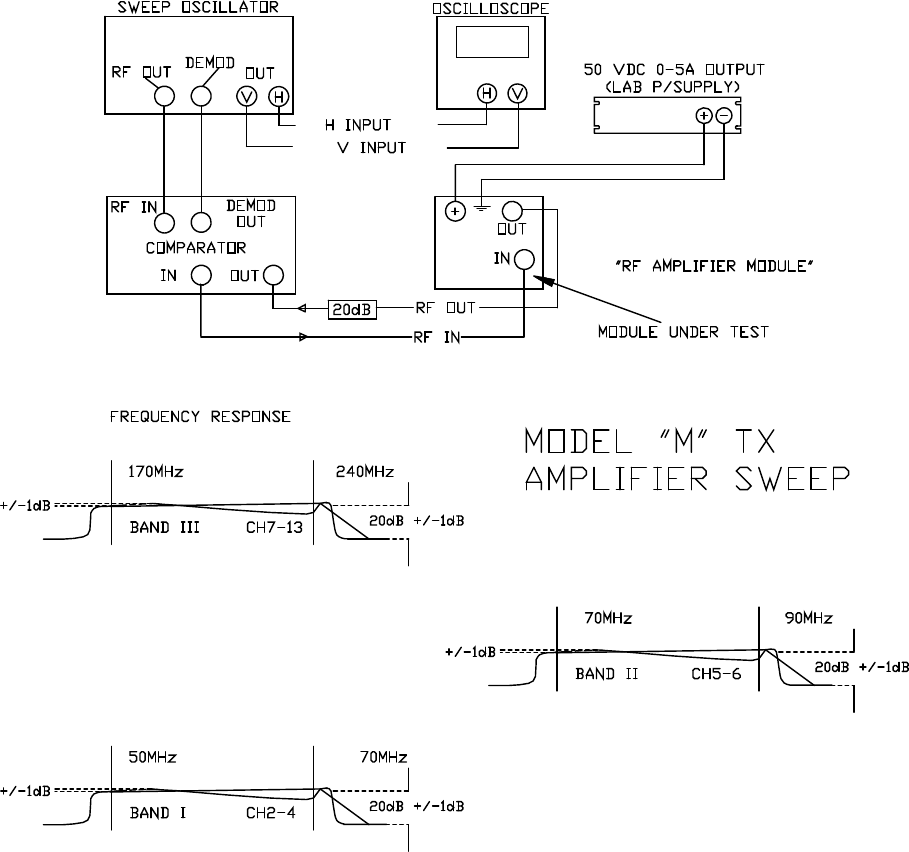
Lowpowersweepofamplifiers
Note:LowpowersweepofPAmodulesshouldnotberequiredundernormalcircumstances–evenwhen
replacingFETdevices.Therearenotuningadjustmentsonthesemodules.
• Ensurethatterminationsareinplaceinthetestsetup.Allmodulesrequire50Ωsourceandload
impedancestopreventdamageandforconsistentresultsduringtesting.
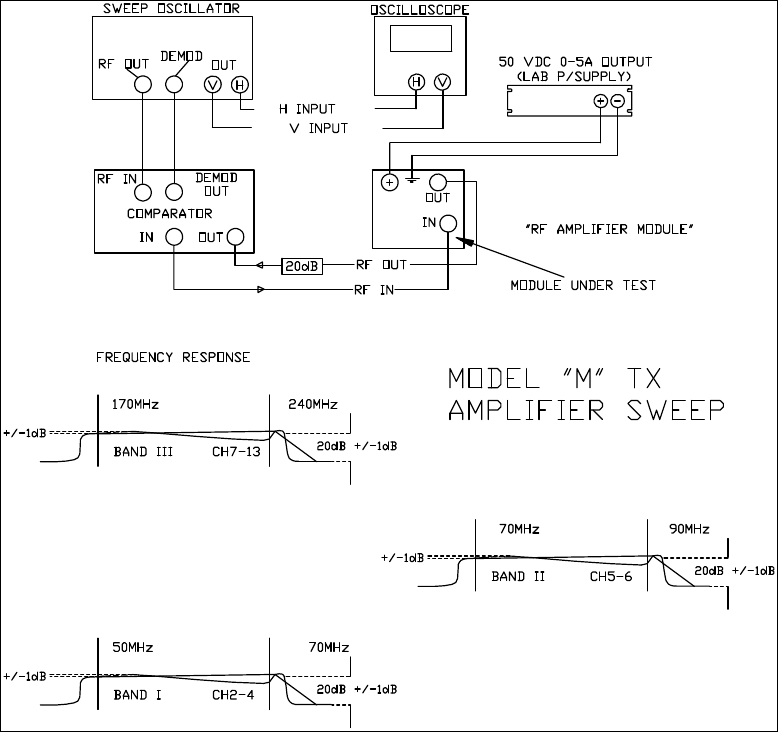
• Connectthemoduletoasweepsystem,typicallyasshowninFigure1.Thesweepgeneratorshouldbe
adjustedtogivealinearsweepfromabout45to75MHz,orfrom65to95MHz,tosweepthepartof
LowBandthatthemoduleisintendedfor,withasmallamountofout‐of‐bandsignalonbothends.
Ensurethatacoaxial20dBattenuatorpadisconnectedtotheRFoutputoftheamplifier,inorderto
preventpossibledamagetothesweepcomparator.
• Connectthelabpowersupply+50Vtothepositivesupplybusbar,andthenegativetothechassisofthe
amplifier.Thecurrentshouldbelimitedto7or8Aforthistest.Caution:observepolarity!
• Withthepowersupplyswitchedon,thecurrentdrawnshouldbenotmorethanthebiascurrentforall
thedevicestogether‐about6amperes(12x0.5A)forthePAmodule.
• Thesweptin‐bandfrequencyresponse,forLowBandmodules,shouldbeessentiallyflatwithin±1dBas
showninFigure1,withgainapproximately20±1dB.
POWERAMPLIFIERLOWBAND
PUB96‐28Rev2Aug.2007 28-5PAModule,
•
Figure1ModulesweepSetup
GreenLEDSensitivityAdjustment
OneofthefunctionsoftheVSWRboardistomonitortheoverallgainofthePAmodule.ThisVSWRboardis
locatedattherearofthemodule,adjacenttotheoutputRFconnector.Forthelocationsofthecomponentson
theboard,pleaserefertoFigure7.
VerifythatallthePAmodulesareingoodworkingorder,andthenproceedasfollows:
• Withallmodulesrunningatnormaloperatingpower,placeAGC/MANUALswitchintotheMANUAL
positionandadjusttheexciteroutputpoweruntilthetransmitteroutputpowerreads110%.
• Removethemoduletobesetup,andremovethetwofrontfusesfromit,inordertosimulateasingle
FETpackagefailure.Replacethis"crippled"moduleinthetransmitter,andapplyanominal50%APL
staircasevideosignaltothetransmitter(analogtransmitters).
• ThegreenLEDshouldnowbeextinguished;ifitisnot,removethemoduleandadjustpotentiometer
(R4)ontheVSWRboardclockwise,replacethemoduleandtryagain,repeatinguntiltheLEDisbarely
extinguishedwhenthemoduleisre‐powered.
• Replacethefusessothemoduleisagainfullyoperational,andverifythatthegreenLEDisnowfully
lightedwhenthemoduleisreplacedinthetransmitterandre‐powered.
POWERAMPLIFIERLOWBAND
PUB96‐28Rev2Aug.2007 28-6PAModule,
o ItisrecommendedthatR4beadjustedonehalfturnatatime,toestablishaknownreference
point.
• PlacetheAGC/MANUALswitchintheAGCposition,andwiththeRAISE/LOWERswitch,readjustthe
transmitteroutputpowerto100%.
• Similarly,theauralamplifiermaybeadjustedinthesamemanner,butbeinganFMsignalthe
modulationofthecarrierisnotcritical.
POWERAMPLIFIER1.5KWHIGHBAND40D1493G3
PUB96‐29Rev2i24Oct2008
CONTENTS
FUNCTIONAL DESCRIPTION .....................................................................................................................................1
6-WAY SPLITTER/INPUT BOARD .............................................................................................................................1
FET RF AMPLIFIERS ...............................................................................................................................................1
6-WAY COMBINER/OUTPUT BOARD .......................................................................................................................2
VSWR CONTROL BOARD G1 ..................................................................................................................................2
GREEN LED SENSITIVITY ADJUSTMENT.................................................................................................................5
POWERAMPLIFIER1.5KWHIGHBAND40D1493G3
PUB96‐29Rev2August2007 29-1PAModule
FunctionalDescription
Drawingreferences:Figure2throughFigure7
ThePowerAmplifiermoduleconsistsofasix‐waypowersplitter,six250WFETamplifiers,asix‐waypower
combiner,aVSWRprotectionboard,andpower&I/Oconnectors.Twofull‐sizeheatsinksprovidethecooling
fortheactivedevices.Itisdesignedfor1.5kWsyncpeakpoweroutputinHighBand174‐230MHzAnalog
televisionsystems,andprovidespowergainofapproximately15‐16dB,with1.5kWpeaksyncvisualor900W
auraloutput.Themodulecanprovideupwardsof250Wofaveragedigitalpowerwhenusedwithappropriate
predistortion.Itisfullyhot‐pluggable,incorporatingprotectivecircuitryforexcessVSWRpowercutback.
6‐WaySplitter/InputBoard
Partnumber:40D1496G1
DrawingReferences:Figure3andFigure4
TheSix‐WaypowersplitterreceivesitsRFinputsignalfromthedrivestageandprovidessixinputsignalsto
integralinputmatchingnetworksforthesixFETamplifiers.Theincomingsignalisfirstsplitinthreebya
three‐wayWilkinsonsplitterandthethreeresultantsignalsaresplitagainbythreetwo‐wayWilkinsonsplitters
toprovidethesixoutputsrequired.Terminationsforthethree‐waysplitterareprovidedbyR109,R110,and
R111,andforthetwo‐waysplitters,terminationsareR101,R103andR105.C115providesinputmatchingfor
thetransitionfromtheinputconnectortotheinputtransmissionline.
Abuilt‐indetector(CR102andC147)isfedfromadirectionalcouplerontheinputtransmissionline,toprovidea
sampleoftheinputsignalformodulegainmonitoring.R113andR117terminatethedirectionalcoupler,
FETRFAmplifiers
DrawingReferences:Figure3throughFigure6
Eachofthesixamplifiersinthemoduleconsistsoftwo,sourcegroundedN‐channel,insulatedgateFieldEffect
Transistors(FETs)packagedinasinglecase,operatingclassABinapush‐pullconfiguration.BecausetheseFETs
are"enhancementmode"devices,theyrequirepositivegate‐to‐sourcebiasvoltageoneachgatetocause
source‐drainconduction.AquiescentClassABidlingbiascurrentissetindependentlyforeachhalf.Thegate
voltagerequiredtoproducethisidlingcurrentmayvarybetween2Vand5Vaccordingtothedevice
specificationsheet,andtheidlingcurrentused.FETgatethresholdvoltagesalsoaretemperaturesensitive,so
thermalcompensationisprovidedbyR9,RT1,andR10,RT2.Biascurrentissetto500mAperhalfofthedevice
foranalogoperationand750mAperhalffordigitaloperation.
Gatebiasissuppliedfromanadjustablevoltagedividerfromthe+39Vregulatedbiasrail.ResistorsR1,R2,R3,
R4providegatebiasforonehalfoftheamplifier;R5,R6,R7,R8providebiasfortheotherhalf.
TheinputRFisappliedtobalunT1/L1toprovidetwosignaloutputs180˚outofphase.Thesesignalsarestepped
downtomatchthelowinputimpedanceofthedevicethroughadualsection,twinπnetworkconsistingofC1,
C2,L2,L3,C7,andthedeviceCG‐S.ThegateimpedanceattheoperatingfrequencyismuchlowerthanR3and
R6,sotheseresistorshavenoeffectatRF.
POWERAMPLIFIER1.5KWHIGHBAND40D1493G3
PUB96‐29Rev2August2007 29-2PAModule
R3andR6provideaDCpathforbias,andprovideloadingatlowerfrequenciesinordertoassistinmaintaining
amplifierstability.ThechoiceofC4andC5values,andtheirinternalequivalentseriesinductances,alsoensures
effectivebypassingatallfrequencies.
Theoutputmatchingπnetwork,consistingofinductorsL5throughL10,andcapacitancesC12throughC16,
tunesouttheFETdraincapacitanceandtransformstheverylowoutputimpedanceoftheFETto12.5ohms.The
two180˚antiphaseoutputsignalsarecombinedinbalunT2,L11.
DCisappliedtothedrainsthroughL4,L5forthe"A"half,andL6,L7forthe"B"half.L5andL6arealsoshort
sectionsofmicrostriptransmissionlinewhichtransformtheapparentRFimpedancesofL4andL7tohigher
valuesasseenbytheFET.RFandlowerfrequenciesarebypassedwithC3,C8,C9,C6,C10,C11.
Thesegroupsofcapacitorsareselectedinvalueandfortheirinternalequivalentseriesinductancessothatthey
willbeaneffectivebypassatallfrequenciesofinterestincludingvideo,toassistinmaintainingstability.Towards
thisobjectiveofstability,inadditiontoresonatingwiththedevicedrain‐to‐draincapacitanceatRF,inductorL9
placesaheavyloadontheFEToutputatlowfrequencies,whereitbehavesasadeadshort.
NotethatfusesareprovidedforthevoltagesuppliedtotheFETdrainconnections.Theintentofthesefusesis
toprotectthesurroundingcircuitryintheeventofadevicefailure.Thenormalfailuremodeofactivedevices
suchastheseisshort‐circuit,andthefusewillblowinthiscase,isolatingthedefectivedevicefromtherestof
themoduleandtransmitterpowersupply,allowingtheremainingdevicestokeepoperatingnormally.Ablown
fusecanserveasavaluabletroubleshootingaid,whentryingtoidentifyfaileddevices.
6‐WayCombiner/OutputBoard
Partnumber:40D1468G1
DrawingReferences:Figure3andFigure6
Thesixamplifieroutputsareappliedtothreetwo‐wayWilkinsoncombinersandphasedelayedtocorrectthe
quadratureconditionimposedbytheinputsplitterboard.ThethreeoutputsoftheseWilkinsoncombinersare
thencombinedbyathree‐wayWilkinsoncombinerintoone50ohm,output.TerminationsfortheWilkinson
networksconsistofR100,R102,andR104forthethreetwo‐way;andR106,R107,R108forthethree‐way
combiner,whichalsorequiresreactivetrimmingfromL100thruL102inorderthatthematchingnetworkcan
accommodatethebandwidthfromchannel7through13.
AdirectionalcouplerfeedsaBNCconnectoronthemodulefrontpanelandcanbeusedforoutputmonitoring.
Thebi‐directionalcouplerprovidesDCsamplesproportionaltoforwardandreflectedpowertotheVSWR
protectionboardformonitoringmodulegainandVSWRprotection.Terminationsforthesecouplerlinesections
areprovidedbyR114,R115,andR118;theRFsamplesforVSWRmonitoringaredetectedbyCR100,C112,and
R112for"forward"andbyCR101,C113,andR116forthe"reflected"direction.
VSWRControlBoardG1
Partnumber:20B1549G1
Refs:20B1594&30C1418(Figure6).
TheVSWRcontrolboardperformsanumberoffunctions:itprovidesregulatedbiasvoltagestotheFETpower
amplifierstages,itprovideshot‐plug‐incapabilitytoprotecttheamplifiermodulewhenpluggedintoan
POWERAMPLIFIER1.5KWHIGHBAND40D1493G3
PUB96‐29Rev2August2007 29-3PAModule
operatingtransmitter,itprovidesprotectiontotheFETsagainstover‐dissipationduetohighVSWR,andit
monitorsthemoduleRFpowergain.
Ifthemoduleispluggedintoapoweredtransmitterusingseveralmodulesrunninginparallel,thepowersupply
connectionsarefirstmadethroughthelongercontactsofthemodule’sDCpowerconnectorandintoVSWR
boardJ1pin8.Thisallowstheelectrolyticbypasscapacitorsofallamplifierstochargethroughcurrentlimiting
resistorR5,preventingoverstressofallamplifierfusesduetochargecurrentofthebypasscapacitors.Whenthe
moduleisfullyseated,thehighcurrentcontactsareconnectedandthemodulecanoperatenormally.
InnormaloperationthepowersupplyentersJ1viapin2,andisregulatedto+39VDCbyseriesresistorR10and
zenerdiodeVR1.RegulatorU1providesconstantB+voltageforop‐ampsU2,U3,U4,andthecomparator
referencevoltages.Whenthemoduleisfirstturnedon(orpluggedin)andU1beginsregulating,thecharging
currentofC7turnsonQ1whichpullsthebiaslinelowforabriefperiodoftime.Thisprovidesaslowstartfor
themoduleafterDCpowerisapplied.
TheoverallRFsystemofthetransmitterprovidesoverallVSWRprotectionviatheexternalRFdetectorboards
discussedinothersectionsofthismanual,butVSWRsensingisalsoprovidedinthemoduleforitsownsafety.
Inthetransmittersutilisingmodulesinparallel,oneormorefailedordisconnectedmodulesorafaultinthe
six‐waycombinerorsubsequent3dBcoupler,maycauseamoduleoutputmismatch.
Tothemodule,anymismatchwhichappearsasreflectedpowerisdetectedandsensedatpin11ofJ1to
comparatorcircuitU2B.
R21setsthelevelatwhichVSWRprotectionbegins.Ifthelevelofdetectedreflectedpoweronpin5ofU2B
exceedsthecontrolvoltagesetonpin6,theoutputonpin7willgohigh.R22,C10,andCR1provideafast
attack,slowreleasecontrolvoltagetoQ2whenahighVSWRconditionsuddenlyoccurs.ThiswillturnonQ2
whichturnsonQ4whichquicklyreducesthebiasappliedtothepoweramplifierFETs;thisreducedbiasalso
reducestheirgainandthereforetheirRFoutputandkeepstheamplifieratsafelevels.
Whenamoduleispluggedintoanoperatingtransmitter,theslowstartcircuitryconsistingofC7andQ1will
initiallykeepthemoduleturnedoff.Powerfromtheothermodulesworkingintothecombinerwillenterthe
moduleandbedetectedbythereflectedpowerdetector.Thiswouldpreventthemodulefromeveroperating
properly,unlesstheVSWRcircuitismomentarilyover‐ridden.
ThecircuitofU4producesapulseapproximately2secondsafterpowerisappliedtothemodule.Atpower‐up,
pin2ofU4willbepulledhighbyC11.R26chargesthiscapacitor,andwhenthepin2voltagegoesbelowthe
voltageonpin3,theoutputofU4willgohigh.ApulsewhosedurationiscontrolledbyC9andR18willthenbe
appliedtopin3ofU2A.U3Bdetectsthatthemoduleisnotproducingforwardpowerandthatthereverse
powerishigh.UndertheseconditionstheoutputofU2Agoeshigh,turningonQ3,momentarilydisablingVSWR
protection,andallowingthemoduletocomeon.
DCsamplescorrespondingtoforwardpowerintoandoutofthemoduleareappliedtoU3Apins2and3
respectively.Whenpin3voltageishigherthanthatofpin2,correspondingto"RFgainisokay"thecomparator
outputU3Apin1ishigh,causingthegreenLEDonthefrontpanelofthemoduletolight.Thecomparison
threshold(ie.modulegainisok)issetbyadjustmentofR4.
POWERAMPLIFIER1.5KWHIGHBAND40D1493G3
PUB96‐29Rev2August2007 29-4PAModule
AdjustmentofbiasvoltagetoestablishproperquiescentFETbiascurrent
Important:50Ωinputandoutputterminationsarenecessarytoachieveconsistentresultsandprevent
damagetothedeviceswhentestingmodules.Supplementalcoolingisnotrequiredwhenperforming
biasadjustmentsorlowpowersweepofthePAmodules.
• Removeallfusesfromthemoduletobetested.(Thereare12fusesintotal).
• Adjustallbiaspotstomaximumresistance,forminimumbiasvoltage.(Again,thereare12).
• UseaclipleadtoshortthejunctionofC5,R6,andR7toground.ThisshutsoffsideBoftheamplifierso
itwillnotinterfere(throughL9)withmeasurementofquiescentcurrentfromsideA.
• TerminatetheRFinputandoutputintoa50Ωload.
• Apply+50VDCfromthefrontpaneltestpointonthetransmitter,throughanammeter,tothepositive
copperbusbar,anditsnegativetochassis.Caution:Observepolarity!
• Checkthevoltageonthebiasterminals,itshouldbe39V±2V.(Thebiasterminalsareconnected
togetherviainsulatedbuswire).
• ReadthecurrentdrawnbytheVSWRboardandbiasregulator.Next,installafuseinsideA(nearestthe
panel)ofamplifier#1;adjustthecorrespondingbiaspotfora500mAincreaseinthepowersupply
current;thisincreasecorrespondstoanidlingbiascurrentof0.5A(750mAfordigitaloperation).
Removethefuse.RemovethesideBbiasshortandplaceitonsideAatthejunctionofC6,R2,R3and
R9.PlacethefuseinsideB.AdjustthesideBbiaspotforthepropercurrent.
• Movethefusetotheremainingfuseholders,oneatatime,andadjusteachcompanionbias
potentiometerinthesamemannerfortheproperbiascurrent.
• Installremainingfusesandremovethebiasshortafterallbiasadjustmentshavebeenmade.
Lowpowersweepofamplifiers
Note:LowpowersweepofPAmodulesshouldnotberequiredundernormalcircumstances–even
whenreplacingFETdevices.Therearenotuningadjustmentsonthesemodules.
• Ensurethatterminationsareinplaceinthetestsetup.Allmodulesrequire50Ωsourceandload
impedancestopreventdamageandforconsistentresultsduringtesting.
• Connectthemoduletoasweepsystem,typicallyasshowninFigure1.Thesweepgeneratorshouldbe
adjustedtogivealinearsweepfrom160to240MHzsothatallofHighBandorBandIIIisswept,witha
smallamountofout‐of‐bandsignalonbothends.
• Connectthelabpowersupply+50Vtothepositivesupplybusbar,andthenegativetothechassisofthe
amplifier.Thecurrentshouldbelimitedto7or8Aforthistest.Caution:observepolarity!
• Withthepowersupplyswitchedon,thecurrentdrawnshouldbenotmorethanthebiascurrentforall
thedevicestogether‐about6amperes(12x0.5A)forthePAmodule.
• Thesweptin‐bandfrequencyresponse,forHighBandmodules,shouldbeessentiallyflatwithin±1dBas
showninFigure1,withgainapproximately15to16dB.

POWERAMPLIFIER1.5KWHIGHBAND40D1493G3
PUB96‐29Rev2August2007 29-5PAModule
Figure1ModuleSweepSetup
GreenLEDSensitivityAdjustment
OneofthefunctionsoftheVSWRboardistomonitortheoverallgainofthePAmodule.ThisVSWRboardis
locatedattherearofthemodule,adjacenttotheoutputRFconnector.
VerifythatallthePAmodulesareingoodworkingorder,andthenproceedasfollows:
• Withallmodulesrunningatnormaloperatingpower,placeAGC/MANUALswitchintotheMANUAL
positionandadjusttheexciteroutputpoweruntilthetransmitteroutputpowerreads110%.
• Removethemoduletobesetup,andremovethetwofrontfusesfromit,inordertosimulateasingle
FETpackagefailure.Replacethis"crippled"moduleinthetransmitter,andapplyanominal50%APL
staircasevideosignaltothetransmitter(analogtransmitters).
• ThegreenLEDshouldnowbeextinguished;ifitisnot,removethemoduleandadjustpotentiometer
(R4)ontheVSWRboardclockwise,replacethemoduleandtryagain,repeatinguntiltheLEDisbarely
extinguishedwhenthemoduleisre‐powered.
• Replacethefusessothemoduleisagainfullyoperational,andverifythatthegreenLEDisnowfully
lightedwhenthemoduleisreplacedinthetransmitterandre‐powered.
POWERAMPLIFIER1.5KWHIGHBAND40D1493G3
PUB96‐29Rev2August2007 29-6PAModule
o ItisrecommendedthatR4beadjustedonehalfturnatatime,toestablishaknownreference
point.
• PlacetheAGC/MANUALswitchintheAGCposition,andwiththeRAISE/LOWERswitch,readjustthe
transmitteroutputpowerto100%.
• Similarly,theauralamplifiermaybeadjustedinthesamemanner,butbeinganFMsignalthe
modulationofthecarrierisnotcritical.
IntermediatePowerAmplifier
30C1892G1‐G2‐G3:
Figures1,2,and7.
The30C1892IntermediatePowerAmplifierbasicallyconsistsofafan‐cooledheatsinkandthreecircuit
boards.TheseboardsarethePreamplifierboard,theAmplifierInputboard,andtheAmplifierOutput
board.Thissubassemblyisequippedwithshieldingcoversandismountedonastandard19"panel.
Figure1showsthebasicconstructionoftheIPAassembly,althoughthedrawingwasoriginallymadefor
asystemusinganadditionalAGCmoduleshownasitem50onthedrawing.AGCintheTTS1000B
transmitterisimplementedintheexciterinstead,soitem50isnotusedandnon‐existentinthepresent
system.
Adirectionalcoupler(showninFigure12)isalsomountedonthepanelandprovidesameteringDC
signalcorrespondingtotheoutputRFfromtheIntermediatePowerAmplifier.
Figures2and7forLowBandandHighBandrespectively,illustratethearrangementofboardsonthe
amplifierheatsink.Drawing30C1474isforour250wattRFpoweramplifier,deratedforIPAservice.
CoolingfortheIPAheatsinkisprovidedbyasmall(approx100cfm)axialflowRotron™fanwhichis
mountedonabracketsituatedsothatthefanblowsaironthefinnedportionoftheheatsink.
RFPreamplifier
10A1453G2(LowBand)and10A1453G3(HighBand):
Figures3and8.
ThispreamplifierdesignoriginallywasusedinthetwoIPAsoftheaural/soundsectionofadualRFchain
transmitterwhichoperatestwosingleRFchainsinquadratureandthereforerequiresphaseandgain
controloftheinputtoeachchain.ItthereforehascomponentsinplaceforadjustmentofRFgainand
phasetoenablesettinguptheseparalleledtransmitters.Inasinglechaintransmittersuchasthe
TTS1000B,norequirementexistsforcontrolofRFphasenorconsequentlyitscomponents,butour
designstandardizationresultsinloweroverallexpensebeingincurredbysimplyleavingthecomponents
onthePCboard.
Thefollowingdiscussiondealswiththephasingcomponentsbecausetheyareapartofthesignalpath
throughthepreamplifier,butfunctionallytheyareinconsequentialexceptfortechnicalinterest.
TheRFinputsignalfromtheexciterisfedviaJ1intoaquadraturehybridU1configuredasaphase
shifter,whichisabletoproduceaphaseshiftinexcessof90°betweenitspin1(input)andpin6
(output).AvaluablepropertyofaquadraturehybridnetworkconnectedasshowninFigures3and8,
isthatitcanintroduceavariablephasedelaythatdependsonthevalueofcapacitanceatits0°and90°
ports.Theseports(U1pins2and5)eachseeapairofvariablecapacitancediodesCR1,CR2andCR3,
CR4.Thecapacitanceofthesediodesdependsontheamountofreversebiasvoltageappliedtothem
fromthearmofR2.Inalltransmitters,R2isadjustablefromthefrontpanelandismarkedPHASE.
IntheLowBandunit,theoutputofthehybridisthenfedviaanattenuatorR5(markedGAIN)toampli‐
fierU2whichisoutputtoterminalJ2.C12andtheleadinductanceofU2performoutputmatchingto
50Ω.ThegainofU2isspec'das18dBandthereareafewdBoflosses,sotheeffectivegainofthe
LowBandpreampboardisabout12to14dBwhenR5isturneduptoitsmaximumoutputposition.
1 kW TTS1000B TRANSMITTER IPA ASSEMBLY
PUB96-30 rev 1: Jul 1, 2010 30-2 1 kW IPA Assembly VHF
IntheHighBandunit,theoutputofthehybridisalsofedviaanattenuatorR5(GAIN)butthistimetoan
additionalpreamplifierstageU4,whoseoutputappearsattheinputofU2,whichfeedsterminalJ2.
Thespec'dgainoftypeMWA330intheU4positionis6dB,andtypeMHW6185orCA2885(U2)is18dB.
AfewdBoflossesexistontheboard,sotheeffectivegainoftheHighBandpreampboard10A1453G3
withR5atmaximumisabout18to20dB.(HighBandpreamps10A1453G1inhigherpowered
externallydiplexedtransmitterauralservice,useatypeMWA130asU4.Specifiedgainisabout12dB,
butsubstitutionofU4intheinternallydiplexedsystemsisnotrecommendedduetooveralllinearity
considerations).
AttheoutputofU2,amatchto50ΩisprovidedbyC12andthedeviceleadinductance,whichtogether
createamatchingnetworkinboardswhereatypeCA2885deviceisused;converselyatypeMHW6185
devicewilldrive50Ωdirectlythereforenospecialoutputmatchingisnecessary,andC12isnotpresent.
MostLARCANexcitersproducetheirbestlinearityatorneartheirmaximumratedoutputlevels,and
oftentheoverallsystemgainissufficienttoresultinoverdriveoflaterstagesofthetransmitter.The
transmitterortranslatorlineupmaythereforeincludeanin‐lineattenuatorintheRFchainaheadofthe
IPAmodule,inordertopreventoverdrivefromcertainmodelsofexciter‐modulator.
U3isavoltageregulatorprovidingB+totheamplifier,andbiasingforthevaractordiodes.
RFisolationisprovidedbyinductorsL1andL2whilecapacitorsC1andC2actasDCblockers.
SRF3943‐2IntermediatePowerAmplifier:
Figures4,5,6,9,10,and11.
TheIntermediatePowerAmplifier(IPA)inboththeLowBandandHighBandversions,isconfiguredin
push‐pull,usingdualN‐channelenhancementmodeFieldEffectRFpowertransistorswhichare
operatedinclassAB.TheIPAcircuitisverysimilartothecircuitofasingleamplifierofthe1.5kWPA
moduledescribedinanotherSectionofthismanual.
TheLowBandandHighBandversionsoftheIPAdifferslightlyduetothefrequencyrangestobe
covered.
LowBandIPACircuitDescription
TheIPAconsistsoftwo,sourcegroundedN‐channel,insulatedgateFieldEffectTransistors(FETs)
packagedinasinglecase,operatingclassABinapush‐pullconfiguration.Theoriginalschematic
indicatesatypeMRF‐151‐GasthedualFETused;actuallywenowusea"selectedMRF‐151‐Gtotightly
controlledspecifications"whichisproprietarytoLARCANanddesignatedtypeSRF3943‐2.The
1 kW TTS1000B TRANSMITTER IPA ASSEMBLY
PUB96-30 rev 1: Jul 1, 2010 30-3 1 kW IPA Assembly VHF
MRF‐151‐Gcouldbeusedasareplacementincaseofdireemergency,buttherearenoguaranteesasto
itsperformance.
BecausetheseFETsare"enhancementmodeN‐channel"devices,theyrequirepositivegate‐to‐source
biasvoltageoneachgatetocausesource‐drainconduction.ThequiescentClassABidlingbiascurrent
issetat0.6ampereforeachhalf.Thegatevoltagerequiredtoproducethisidlingcurrentmayvary
between2Vand5Vaccordingtothedevicespecificationsheet,andtypicallyis3to4V.FETgate
thresholdvoltagesalsoaretemperaturesensitive,sothermalcompensationisprovidedbyRT1andRT2.
Gatebiasissuppliedoutofadjustablevoltagedividersfrom+20VregulatedbiassourcesCR1andCR2.
CurrentlimitingtothesezenerdiodesisprovidedthroughR1andR8.ResistorsR9,R2,R3,R4,andRT1
providegatebiasforthe"A"halfoftheamplifier;R10,R7,R6,R5,andRT2providebiasforthe"B"half.
TheRFinputsignalarrivinginJ1isappliedtobalunT1toprovidetwosignals180°out‐of‐phase.These
antiphasesignalsaresteppeddowntomatchthelowinputimpedanceoftheFETthroughaπ‐network
consistingofC1,C2,C3,L1,L2,C4,andthedeviceinputcapacitance,andthenappliedtothegates.
ThecapacitancevalueofC4ischangedforoperationonchannels5&6.Thegateinputimpedanceat
theoperatingfrequencyislowcomparedwiththevaluesofR3andR6,whichhavelittleornoeffectat
RF.
R3andR6provideaDCpathforbias,andprovideloadingatlowerfrequencieswheregateimpedanceis
high,inordertoassistinmaintainingamplifierstability.ThechoiceofC6,C7,C20,andC21values,
theirseriesinductances,andthatofboardtraces,alsoensureseffectivebypassingatcritical
frequencies.
Theoutputmatchingπ‐network,consistingofinductorsL3thruL8,andcapacitancesC13thruC16,
transformstheverylowoutputimpedanceoftheFET,upwardstoastandard50Ω.Thetwoantiphase
outputsignalsarefinallycombinedinbalunT2,L9.JumpersplacedacrosspartsofL7andL8,plusthe
changedvaluesofC13,C14,C15andC16,configuresthesystemforchannels5&6operation.
DCisappliedtotheFETdrainsthroughL3,L4fortheQ1Ahalf,andL5,L6fortheQ1Bhalf.L3andL6
areshortsectionsofmicrostriplinewhichtransformtheapparentRFimpedancesofL4andL5tohigher
valuesasseenbytheFET.RFandlowerfrequenciesarebypassedwithparalleledC9,C10,andC17for
the"A"halfoftheamplifier,andC11,C12,andC18forthe"B"half.Thesegroupsofcapacitorsare
selectedinvalueandfortheirinternalequivalentseriesinductancessothattheywillbeaneffective
bypassatcriticalfrequenciesofinterest,includingvideo,toassistinmaintainingstability.The
connectionsforC20andC21alsoassistinstabilityduetotheirreturnpathsthroughthegroundplaneof
theoutputboard.Thisconnectionprovidesasmallamountofnegativefeedbackasaprimitivemeans
ofneutralizingtheamplifier.
TheRFoutputleavestheboardfromJ2.
LBIPASetupProcedures
1 kW TTS1000B TRANSMITTER IPA ASSEMBLY
PUB96-30 rev 1: Jul 1, 2010 30-4 1 kW IPA Assembly VHF
1.Setupa50Vpowersupply,currentlimitedtoalittlemorethan1.2amps.
2.Turnbothbiaspotentiometerstotheirmaximumresistanceposition.Removebothfuses.
3. SRF3943‐2IntermediatePowerAmplifier:LBSetup,continued.
3.Applythe50Vsupplytoonetransistoratatime(onehalfpackage)andadjustthecorrespondingbias
resistorfor600mAdraincurrent.Thesesettingsareastartingvalue,whichwillbereadjustedduring
systemtest,forminimumintermodsandFMnoise.
4.Connecta30dB,20Wattenuatortotheoutputoftheamplifier.Thiswillabsorbamplifieroutput
andprotectthesweepdetector.Useitinsteadofthe20dBpadshowninthediagrambelow.
5.ReinstallfusesandapplyB+tobothsupplyconnectionsoftheamplifiermodule.
6.ApplyalowlevelsweeptotheamplifierandmeasuretheDCinputcurrent(notmorethan1.2amps)
andgain.Gainoftheamplifieraloneshouldbeabout20to24dB,andwiththepreamp(R5at
maximum)thecombinedgainshouldbebetween32and38dB.Flatnessoverthebandshouldbe
betterthan1dB,asshowninthefollowingdiagram.Curvesforchs2‐4and5,6arecorrect:
PUB96-30 rev 1: Jul 1, 2010 30-5 1 kW IPA Assembly VHF
1 kW TTS1000B TRANSMITTER IPA ASSEMBLY
1SweepsetupandresponseforIPAalone,withoutpreamp.
1 kW TTS1000B TRANSMITTER IPA ASSEMBLY
PUB96-30 rev 1: Jul 1, 2010 30-6 1 kW IPA Assembly VHF
HighBandIPACircuitDescription
TheIPAconsistsoftwo,sourcegroundedN‐channel,insulatedgateFieldEffectTransistors(FETs)
packagedinasinglecase,andoperatinginapush‐pullconfigurationinclassAB.TheseN‐channelFETs
are"enhancementmode"devices,sorequireapositivegate‐to‐sourcebiasvoltageoneachgateto
causesource‐drainconduction.QuiescentClassABidlingbiascurrentissetat0.6ampereforeach
half.
Thegatevoltagerequiredtoproducethisidlingcurrentmayvarybetween2and5Vduetovariances
amongFETs,andtypicallyis3to4V.Gatevoltagesalsoaretemperaturesensitive,sotemperature
compensationisprovidedbyRT1andRT2.
Gatebiasissuppliedoutofadjustablevoltagedividersfrom+20VregulatedbiassourcesCR1andCR2.
CurrentlimitingtothesezenerdiodesisprovidedthroughR2andR8.ResistorsR9,R1,R3,R4,andRT1
providegatebiasforthe"A"halfoftheamplifier;R10,R7,R5,R6,andRT2providebiasforthe"B"half.
TheinputRFarrivinginJ1isappliedtobalunT1,L1toprovidetwosignaloutputs180°outofphase.
Thesesignalsaresteppeddowntomatchthelowinputimpedanceofthedevicethroughadualsection,
twinπnetworkconsistingofC1,C2,L2,L3,C3,andthedeviceinputcapacitance,andthenappliedtothe
gates.ThegateimpedanceattheoperatingfrequencyismuchlowerthanR3andR5,sothese
resistorshavelittleornoeffectatRF.
R3andR5provideaDCpathforbias,andprovideloadingatlowerfrequenciesinordertoassistin
maintainingamplifierstability.ThechoiceofC2andC6values,andtheirinternalequivalentseries
inductances,alsoensureseffectivebypassingatcriticalfrequencies.
Theoutputmatchingπnetwork,consistingofinductorsL5thruL10,andcapacitancesC12thruC16,
tunesouttheFETdraincapacitanceandtransformstheverylowoutputimpedanceoftheFET,upwards
toastandard50ohms.Thetwo180°antiphaseoutputsignalsarefinallycombinedinbalunT2,L11.
DCisappliedtothedrainsthroughL4,L5forthe"A"half,andL6,L7forthe"B"half.L5andL6arealso
shortsectionsofmicrostriptransmissionlinewhichtransformtheapparentRFimpedancesofL4andL7
tohighervaluesseenbytheFET.RFandlowerfrequenciesarebypassedwithC1,C10,C11,andC8,
C9,C7.
Thesegroupsofcapacitorsareselectedinvalueandfortheirinternalequivalentseriesinductancesso
thattheywillbeaneffectivebypassatallfrequenciesofinterestincludingvideo,toassistinmaintaining
stability.Towardsthisobjectiveofstability,inadditiontoresonatingwiththedevicedrain‐to‐drain
capacitanceatRF,inductorL9placesaheavyloadontheFEToutputatlowfrequencies,whereit
behavesasadeadshort.
HBIPASetUpProcedures
1.Setupa50Vpowersupply,currentlimitedtoalittlemorethan1.2A.
1 kW TTS1000B TRANSMITTER IPA ASSEMBLY
PUB96-30 rev 1: Jul 1, 2010 30-7 1 kW IPA Assembly VHF
2.Turnbothbiaspotentiometerstotheirmaximumresistanceforminimumbias.ShortC6withaclip
lead.Thiszero‐biasesthe"B"halfsoitdoesnotinterfere(viaL9)withthe"A"halfbeingadjusted.
3.ApplythesupplytotheB+terminalsandadjustR1bias‐adjustpotentiometerfor600mAdraincurrent
onside"A".Turnoffthesupply,changetheclipleadtoshortC2insteadofC6,turnonthesupply
again,andadjustR7bias‐adjustpotentiometerfor600mAdraincurrentonside"B".
Thesewillbethestartingpoints;thebiascurrentsettingsandL9willbereadjustedduringsystemtest,
forminimumintermodsandFMnoise.Disconnecttheclipleadafteradjustingbiascurrents.
4.Connecta30dB20Wattenuatortotheoutputoftheamplifier.
5.ApplyB+tobothsupplyconnectionsoftheamplifier.
6.ApplyalowlevelsweeptothemoduleandmeasuretheDCinputcurrent(about1.2amps)andgain.
Amplifiergainbyitselfshouldbe15to17dB,andwithpreampincludedandR5atmaximum,overall
gainshouldbebetween33and37dB.Sweepresponseshouldbeflatwithin1dBoverthebandas
showninthesweepdiagramfrompage4,repeatedbelow.Notethatthesweepcurvesareapplicable
tothepush‐pullFETamplifieronlyandthepreampisnotincluded.
CONTENTS
CONTROL AND METERING PANEL...........................................................................................................................1
TRANSMITTER CONTROL CIRCUIT BOARD ASSEMBLY ...........................................................................................1
ControlandMeteringPanel
40D1985G1
TransmittercontrolandmonitoringisperformedbytheControlandMeteringPanel.This19"wide,3unit(53")
panelservesprimarilyasamechanicalmountingforthetransmitter'scontrolswitches,statusindicatorlights,
andamultifunctionmeter.Italsoisthemountingforthecontrolcircuitboarddescribedbelow,andforan
outputmeteringcircuitboard.
Thetransmittercontrolpanelfeaturesasseenfromthefront,are:
• Apanelmetercalibrated0‐125percent,anda0‐100linearscale;
• Themeterinputselectorswitchforforwardandreflectedpower,IPAoutputlevel,andAGCvoltage;
• PushbuttonsforON,OFF,REMOTE/LOCAL,AGCON/OFF,TXRESET;
• AscrewdriveradjustedpotentiometerforthedesiredAGClevel,hencetransmitteroutputpower;
• FiveLEDsprovidingindications(fromlefttoright)whenlighted:
o EXT1interlockisclosed,
o theoutputamplifierTEMPthermostatiscool,
o EXT2interlockisclosed.
o VSWRL/OwhenlightedmeansthreemajorVSWReventshaveoccurredduringashorttimeand
thetransmitterisnowofftheair,and
o VSWRC/BlightsupduringaVSWReventthatissufficienttocausethetransmitterpoweroutput
todecrease,oreventomomentarilyturnoffthetransmitter.
ThetransmitterisprovidedwithaVSWRcutbackfunctionthateitherreducesitspoweroutputtosaveitfrom
harmintheeventofgradualoccurrencessuchasantennaicebuild‐up,ormomentarilytakesitofftheairfrom
randomevents.
ThreeVSWReventsoccurringrapidlyinashorttimewillcausetheVSWRLockoutmodetoturnthetransmitter
offuntilitisreset.RandomVSWReventsnormallydonotcauselockoutunlessthereflectionissustained,
causingrepeatedmomentarytrippingandultimatelockout.Antennaorlinedamageoccasionallycanbeafactor,
butusuallyiceaccumulationontheantennacausessustainedhighVSWR.
TransmitterControlCircuitboardAssembly
30C1829G1
SeeFigure1andFigure2.
TherearesevenconnectorsontheControlcircuitboard.Theseconnectorsperformthefollowingfunctions:
• J1interconnectswithJ3oftheMeteringboardviaa34‐wireribboncable.
• J2connectselsewhereinthetransmitter,suchastheexciterandthePA,andtothemeter.
• J3connectstotheexternalinterlocks,andanyspeciallocalcontrolsforTXoffandonfunctions.
• J4interconnectswithJ4oftheMeteringboardfortheAGCpotentiometerandswitchwiring.
• J5isa15‐contactD‐shellconnectorprovidedforuserremotecontrolsystem.
PUB96-32 Rev 2 August 29, 2005 32-1 TX Control Panel 40D1985G1
• J6interconnectswithJ5oftheMeteringboardfortheAGC,VSWRcutback,andVSWRshutdownsignals.
• J7istheconnectiontotheAGCfeedbackinputoftheexciter.
Thetransmitterinterlockchainbeginswiththe+12VatK1‐7.WhenK1issetONbyenergizingitscoilK1‐1,
contacts7and12closeandcontacts7and10open,turningofftheLEDinsidetheOFFbuttonS4.The+12Vfrom
closedcontact7‐12lightstheLEDinsidetheONbuttonS3andlightstheopto‐diodeinU3D,whichprovidesa
logicalactivelowoutofitspin10foraremotecontrolstatusinterface.Thisstatussignalsimplytellstheremote
controlthroughJ5‐6thatthetransmitterwasinstructedtobeON,nothingmore.
The+12Vfromcontact7‐12alsocomesoutoftheboardonJ3‐5,whichisonesideoftheEXT1interlock.EXT1
inlargertransmittersisoftenusedwithafirealarmsystemtostopallblowers,andinlowerpowertransmitters
itisstillworthwhilethatanormallyclosedfirealarmcontactbeconnectedtoEXT1becausethefan(s)inthe
transmittercouldcauseenoughaircurrentsinthetransmitterroomtofantheflames.
WhentheEXT1interlockisclosedandthe+12VappearsonJ3‐4,the+12VisnowatDS5(markedEXT1)andthe
opto‐diodeofU3CwhichbothlightuptosayEXT1isclosed.TheactivelowfromU3Cpin11informstheremote
controlviaJ5‐14thatEXT1interlockisclosed.
The+12VnowisappliedtoJ2‐8whichconnectstoanormallyclosedcontactinathermostatthatrespondsto
thetemperatureoftheRFpoweramplifier.Ifacoolingfanshouldstopandtheamplifiershouldoverheat,this
contactwillopenandpreventthe+12VfromappearingatJ2‐3.Thisofcoursebreaksthechainandremovesthe
12Vfromthesolenoidofthepowersupplycontactor.
Assumingthethermostatiscool,DS4andtheopto‐diodeinU3Barelighted,confirmingTEMPisokay.The
logicalactivelowoutofU3Bpin14informstheremotecontrolofthisfactthroughJ5‐7.
Nextstopforthe+12VisanormallyclosedVSWRlockoutrelaycontactconnectedviaJ1‐5andJ1‐9fromthe
MeteringBoard(Prefix5A,K2).Thisrelayoperatesandtheinterlockchainisopened,ifforsomereasonthe
transmitterhasseenalargeamountofreflectedpowerandtheMeteringBoardVSWRsupervisorycircuithas
repeatedlytriedandretriedtokeepthetransmitteronandfinallydecided"Enough!"TheVSWRlockoutrelay
canberesetfromRESETbuttonS6,orbytheVOREnableand/orRemoteONviajumpersE1,E3.
AssumingtheVSWRislowand5A‐K2contactsareclosed,the+12VnextappearsatJ3‐3,whichisEXT2
interlock.ThisistheplacewhereRFpatchpanellinkcontactsorcoaxialswitchauxiliarycontacts,and/ordummy
loadthermostatcontactswouldbeconnectedsothatthetransmittercanonlybeONwhenvalidRFpathsare
present,consequentlytheEXT2pathfromJ3‐3toJ3‐7willbeintact.
Finally,whentheinterlockchainiscomplete,the+12Visappliedtothesolenoidofthepowersupplyprimary
contactorthroughJ2‐10,andthecoolingfansandpowersupplyareallturnedon.TheDS3LEDmarkedEXT2is
lighted,asistheopto‐diodeinU3A.TheoutputactivelowfromU3Aatpin15informstheremotecontrolvia
J5‐15thattheEXT2interlockisintact.
Theinterlocked+12VisalsoavailableatJ3‐6soitcanbeusedforspecialon‐sitecontrolfunctions.
ThetransmittercontrolcircuitpermitsthetransmitteralwaystobeturnedOFF.Any+12VappliedtotheK1
Resetcoilatpin6willcausethe+12Vtoberemovedfromtheinterlockchaindiscussedabove,anddiverted
insteadtotheLEDinsidetheOFFbuttonS4.Thefactthatturnoffispossibleregardlessofthepositionofthe
REMOTE/LOCALswitch,isavaluablesafetyfeatureprovidedinallLARCANtransmitters.
ThetransmitterAGCsystemisbasedonanRFattenuatorlocatedneartheoutputstageoftheexciter,andthisis
controlledbyDCvoltagesuppliedfromRFdetectorswhichsampletheRFoutputfromthetransmitter.Ifthe
PUB96-32 Rev 2 August 29, 2005 32-2 TX Control Panel 40D1985G1
PUB96-32 Rev 2 August 29, 2005 32-3 TX Control Panel 40D1985G1
outputrises,theDCvoltageincreases,andthisincreasestheamountofattenuation,thustheoutputis
maintainedataconstantlevel.TheAGCprocessingisdonebyanalogop‐ampcircuitsintheMeteringBoard,but
theinitialthresholdsettingisdoneintheControlboardfromAGCswitchS5andAGCpotentiometerR9.These
simplyprovideanadjustablereferencebiasvoltagetotheAGCcircuit,whichadjuststhepoweroutputinversely
accordingtothisbiasvoltage.WhenS5isopen(theLEDinS5isoffandAGCisDisabled),R9risestothe+12Vrail
oftheMeteringBoardandtheAGCprocessingstageinvertsthishighvoltagesoitsoutputandthustheAGC
voltageisverylow,resultinginmaximumexciteroutput.ExciteroutputispreadjustedwithAGCoff,tomake
110%transmitterpower.
IntheeventofaVSWRthatexceedsapresetamount,theAGCvoltagebecomesmodifiedalittletoreducethe
transmitteroutputbyanamountproportionaltothereflectedsignal.This"VSWRCutback"permitsthe
transmittertoremainontheairatreducedpoweriftheantennashouldgraduallyaccumulatealayerofice.If
thereflectedpowershouldexceedamuchlargeramountcausingrepeatedmomentarytrippingoffairandthe
VSWRsupervisorycircuitattemptstorestoretransmitteroperationbutcannotandthenlocksout,thentheAGC
voltageiscutdownevenmore.Thisiscalled"VSWRShutdown."
TheAGCvoltageandmodificationstoitfromVSWR,aresummedinU2Awhichisbasicallyabufferamplifierthat
alsoprovidesatelemetryoutputtotheremotecontrolsystemthroughJ5‐3.
R15setsthecalibrationofthemeterwhenitreadsfromtheAGCpositionofthemeterselectorswitchS1.
R1setsthecalibrationofthemeterwhenitreadstheIPAoutputlevelfromtheIPApositionofS1.
ForwardandReflectedmetercalibrationisdonewithpotentiometersontheMeteringBoard.
VHF OUTPUT RF METERING & AGC CIRCUIT BOARD
PUB96-33 rev 1: May 16, 1997 33-1 RF Output Metering 20B1299G3
).
.
er
carriers.
1kW
this
Contents:
Sec TopicPage
1 RFMetering&AGCBoardDescription1
2 RFMeteringBoardTestandCalibration3
RFMetering&AGCBoard
20B1299G3:
Figures1and2.
Thisboardservesseveralfunctions:AGC,VSWRsupervision,forward&reflectedpowermetering,and
telemetry.Exceptfortheirfunctionsandinputnames,meteringboardshaveidenticalRFdetectors.
Forthisreason,Detector#1for"Forward"willbedescribed,and#2for"Reflected"willbereferencedby
itscomponentnumbersinsideparentheses(
RFDetectors:
The#1Forward(#2Reflected)RFpowersampleisappliedtoJ1(J2)andisterminatedbyR2(R4).A
smallamountofforwardbiasisappliedtoCR1(CR2)viaR1andR5(R3,R6)toovercomethethreshold
voltageofthediodeandenhanceitsdetectionlinearityatlowsignallevels.Theopposingconnection
ofCR1(CR2)diodejunctionandQ1(Q2)emitter‐basejunctionprovidestemperaturecompensation
Q1(Q2)bufferamplifierprovidesalowimpedancesourcetodrivethetrapC3,C4,andL1(C5,C6,L2),
throughR9(R10).Thistrapisbroadlyresonantto4.3MHz,andsignificantlyattenuates3.58MHz
NTSCcolorsubcarrieraswellasany4.5MHzintercarrierthatmaybegeneratedinCR1orCR2dueto
thepresenceofvisualandauralRFsignalstogetherinthesystem.Removalofthesesubcarrier
componentsbeforethesignalispeakdetected,enablesthecircuittoberesponsivetosyncpeakpow
only(forvisual)orjustCW(aural)power,andrelativelyimmunetoundesired
CR3(CR4)isapeakdetectorwithatimeconstantsetbyC7andR11(C8,R12).Thesignalfromthis
peakdetectorisfedtoop‐ampU1(U2)pin5.Thegainofthisstageis2x(4x),anditsoutputonpin7
feedstelemetryandmeteringsignalstotheoutsideworld.IntheboardusedasPrefix5Ainthe
transmitter,pin7alsofeedsvoltagesforAGC(VSWRsupervision)tothepin3secondhalfofU1(U2).
Theseop‐ampsareusedinthemainAGCandVSWRfunctionsofthetransmitter.
U1(U2)outputpin7zero‐offsetvoltageiscontrolledbyR18(R20).ThispotshouldbesetwithnoRF
input,sothatwhileyouwatchthevoltageonTP1(TP2)asyouaresettingthepot,youwillobservethe
decreaseofthevoltagetowardszero.Whenitceasesdecreasing,stopadjusting.Expectabout20
mVoffsetvoltagewhentheop‐ampoutputisalmosttouchingground.Ifthepotisturnedbeyond
point,theoutputstageoftheop‐ampwillbedrivenintosaturationthusunabletorespondtolow
powerlevels.
VHF OUTPUT RF METERING & AGC CIRCUIT BOARD
PUB96-33 rev 1: May 16, 1997 33-2 RF Output Metering 20B1299G3
is
output.
d
ve.
TheoutputofU1‐7(U2‐7)drivestheRFpowermeterthroughR32(R30)whichsetthemeterdeflection
withaknownRFsignal.U1‐7(U2‐7)drivesthetelemetrybufferU4throughR29(R47)whichare
adjustedtocalibratethetelemetrytoastandardvoltagewithaknownRFsignal.Forwardcalibration
isdonewithfullratedpowerandaforwardRFsamplefromtheprobesectionappliedtoJ1.R29
adjustedfor3.0VDCdeliveredtoJ3‐6,andR32isadjustedfora100%readingontheforwardpower
meterposition.
ForReflectedcalibration,thesameforwardRFsampleisthenappliedthrougha16dBpadtoJ2,and
R47isadjustedfor1.5VDCatJ3‐10,andR30issetfora2.5%readingontheReflectedPowermeter.
Becauseoftheextra16dB,thecalibrationautomaticallygetsax40multiplier,sotheactualreadingof
themeteris2.5%onafullscaleof12.5%.Thefirstscalemarkofthemeteristhen0.5%.Ifyouwere
tosubstitutea10dBpadforthe16dBandadjustR36andR49togettheVSWRsupervisionlevelsoutof
theway,youwouldseeameterdeflectionof100%whichcorrespondstoactual10%reflectedpower,
andatelemetryoutputvoltageof3.0VDC.Itissimplytheinsertionofthepadandthesubsequent
calibration,thatprovidesthemetermultiplierscalefactor.
Whenyouaresettinguptheadjustmentsonthisboard,disabletheAGC,andsettheexciterlevelfor
100%RFoutputfromthetransmitter.ThisisespeciallytrueforthereflectedorVSWRsettings,
becausethesearedoneataforcedRFlevelthatishighenoughthattheAGCsystemwillbedriveninto
cutbackmodewhichiswhatwillneedtobesetupbecauseitaffectstheexciter
AGCandVSWRsupervision:
TheoutputfromU1(U2)pin7isalsoappliedtoasecondop‐ampU1(U2)pin3.Ifthedetectedlevel
atU1pin3risesabovethelevelsetbytheAGCpot(ontheControlboard)atU1pin2,theoutputonpin
1willrise.ThisAGCoutputisappliedviaJ5‐1toafinalbufferamplifier(U2AontheControlboard)an
fromtheretoaPINattenuatorintheexciter,therebyreducingthetransmitterpoweraccordingly.
ThereflectedpowerdetectorCR2,Q2,CR4,U2issimilarinoperationtotheforwardpowerdetector
CR1,Q1,CR3,U1.Ifthereflectedpowerrisestoavaluehigherthanacalibratedvalueof17to18dB
belowtheforwardpowerlevel,thenpin3ofU2risesabovethevoltageonpin2thatissetbythe
adjustmentofR36,U2pin1willgohigher,whichappliesadrivecutbacksignalviaJ5‐2toU2Ainthe
ControlboardandfromtheretothePINattenuatorintheexciter.Atthesametime,U3pins3and6
arealsodrivenmorepositi
WhenthevoltageonU3‐3exceedsthevoltageonU3‐2thatisdeterminedbytripthresholdcontrolR42,
U3‐1goesHIGH,tooutputastatussignalHIGHthroughbufferQ4,andtoenergizeVSWRtriprelayK1
thrubufferQ3.ThebaseofQ3insometransmittersmayhaveatimedelayR61,C21added,toavoid
falseVSWRtrippingafterpowerfailureandrestoration.Thecomponentpartsforthis"fix"maybe
solderedtothebackoftheboardinRev4andearlier.
Ifthereflectedpowerincreasesstillfurther,thevoltageonU3‐6risespastthevoltagethresholdsetby
R49onU3‐5,thenU3‐7willswitchLOW,whichtriggersthe"555"timerU5.ThisICwillproducean
outputpulseatU5pin3ofapproximatelyonesecondduration.ThispulseisalsoappliedtothePIN
attenuatortotemporarilyremoveRFdrive.Restorationofthetransmittershouldnormallyhappen
VHF OUTPUT RF METERING & AGC CIRCUIT BOARD
PUB96-33 rev 1: May 16, 1997 33-3 RF Output Metering 20B1299G3
kout.
‐adjustR18.
,
ached,donot
‐adjustR20.Thisadjustmentisdoneinpreciselythesamewayasinstepa)above.
lPower"),thenadjustR29foratelemetry
utputreadingof3.0VDCmeasuredatU4pin7orJ3‐6.
dpowermeterupperscale
ads25.Thisnowcorrespondstoanactualreflectedpowerof1/40(2.5%).
s
orrespondingto10%powerlevelwillthenbe2.0VDC.Mostremotecontrolsystemscan
afteroneortwooccurrences.Thethirdoccurrencewithinapredeterminedtime(C20,R51)should
causeloc
IfenoughVSWReventswithinashorttime,oronesustainedoccurrence,causesU5toproducethree
pulsesinrapidsuccession,C20acquiresasufficientchargethruR51toraisethevoltageofpin5of
comparatorU6higherthanitsreferencevoltageonpin6,thenQ5willbedrivenHIGHwhichenergizes
relayK2,thuslockingoutthetransmitter.
When+12Vregulatedpoweristakenfromthecompanionexciter,regulatorVR1isnotneedednorused.
RFMeteringBoardTestandCalibration:
ForwardPowerMeterCalibration‐ZeroAdjust
WithnoRFinputconnected,measuretheDCvoltageatU1‐7(orTP1)andadjustR18untiltheoutput
voltageatU1‐7(TP1)dropstoaminimum,approximately10to20mVDC.ADCcoupledscopewill
maketheadjustmenteasiertosee;theobjectiveistoplacetheU1outputasneartheop‐ampground
railaspossiblewithouttheop‐ampgoingintosaturation.Turningthepotfartherwilldecreasethe
sensitivityofthesystemforsmallsignals.Oncethisminimumvoltagehasbeenreached,donot
re
ReflectPowerMeterCalibration‐ZeroAdjust
WithnoRFinputconnected,measuretheDCvoltageatU2‐7(orTP2)andadjustR20foraminimum
whichshouldbeapproximately20mVDC.Oncethisminimumvoltagehasbeenre
re
ForwardPowercalibrationandTelemetry
TurnofftheAGCandsettheexciterRFoutputforthetransmittertorunatratedpeaksync(orat
maximumlicensedpower,whicheverisless;callthis"Ful
o
ReflectedPowercalibrationandVSWRTripSettings
Withthetransmitterstillat"fullpower",disconnecttheRFinputcablefromJ1andconnectitinsteadto
thereflectedpowerinputJ2viaa16dBpad.AdjustR30sothatthereflecte
re
AdjustR47sothatthetelemetryoutputatU4pin1reads1.5VDC.Thisisthevoltagethatcorrespond
to2.5%power.Fullscale10%powerwillbe3.0VDC.Wearereadingafront‐panelmeterwhose
scaleiscalibratedtoasquarelawsoitdisplayspower,andwewantthecorrespondingvoltage.Inthe
eventthatthecircuitcannotdeliver1.5VDC,gofor1.0VDCinstead.Thetelemetryvoltage
c
accommodatethis.
VHF OUTPUT RF METERING & AGC CIRCUIT BOARD
PUB96-33 rev 1: May 16, 1997 33-4 RF Output Metering 20B1299G3
djustR36tocutbacktheoutputofthetransmitteruntilthereflectedpowermeterupperscalenow
iththe16dBpadstillincircuit,adjustR42untilK1energizes,andthe"VSWRC/B"indicatorLEDon
ulse.Afterthreepulses(visibleonthemeter),lockoutandared"VSWRL/O"indicationonthe
ontrolPanelshouldoccur.CheckthatRESETispossibleusingtheRESETbuttonS6ontheControl
Panel.
A
reads20(2.0%).Thisisabout17to18dBbelowthefullforwardpoweroutputofthetransmitter.
W
theControlPanellightsup.
Replacethe16dBpadwitha10dBpad,andadjustR49slowlyuntilU3‐7goesLOW,causingU5to
p
C