Larcan MXI1002U Digital Television Translator User Manual Heading 3
Larcan Inc Digital Television Translator Heading 3
UserManual.wiki
>
Larcan
>
MXI1002U User Manual
>
Amplifier Control PUB
Contents
1.
Amplifier Chassis PUB
2.
Power Amplifier PUB
3.
Controller PUB
4.
Operations/Maintenance PUB
5.
Combiner PUB
6.
Power Supply PUB
7.
Amplifier Control PUB
Amplifier Control PUB
Navigation menu
Upload a User Manual
Namespaces
Wiki Guide
HTML
PDF
Info
Views
User Manual
Discussion / Help
Navigation
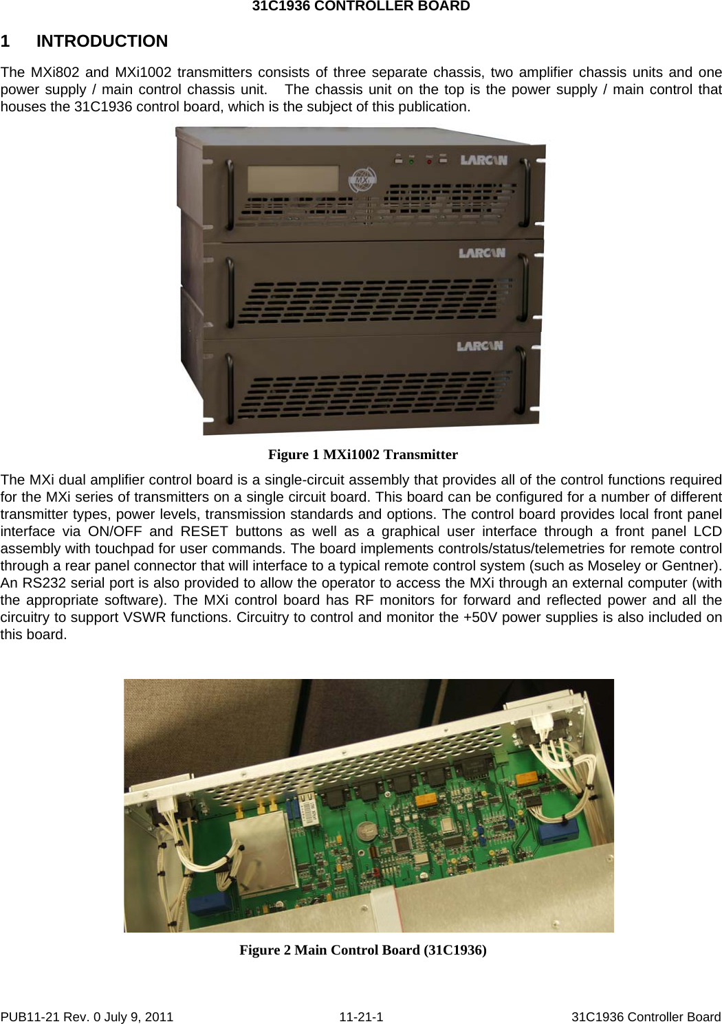
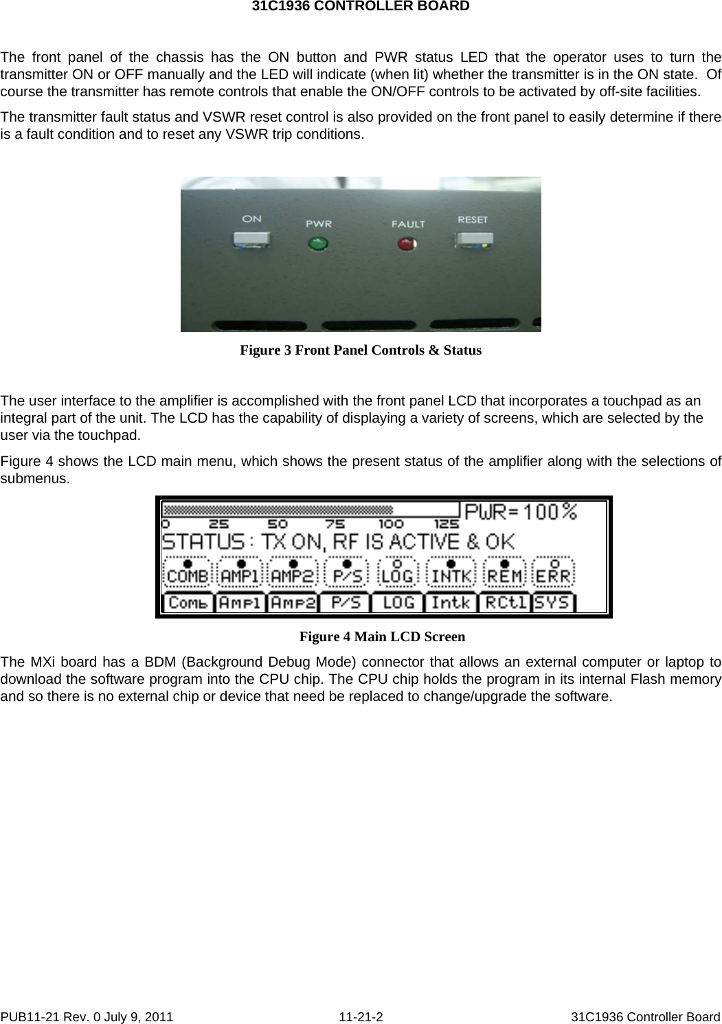
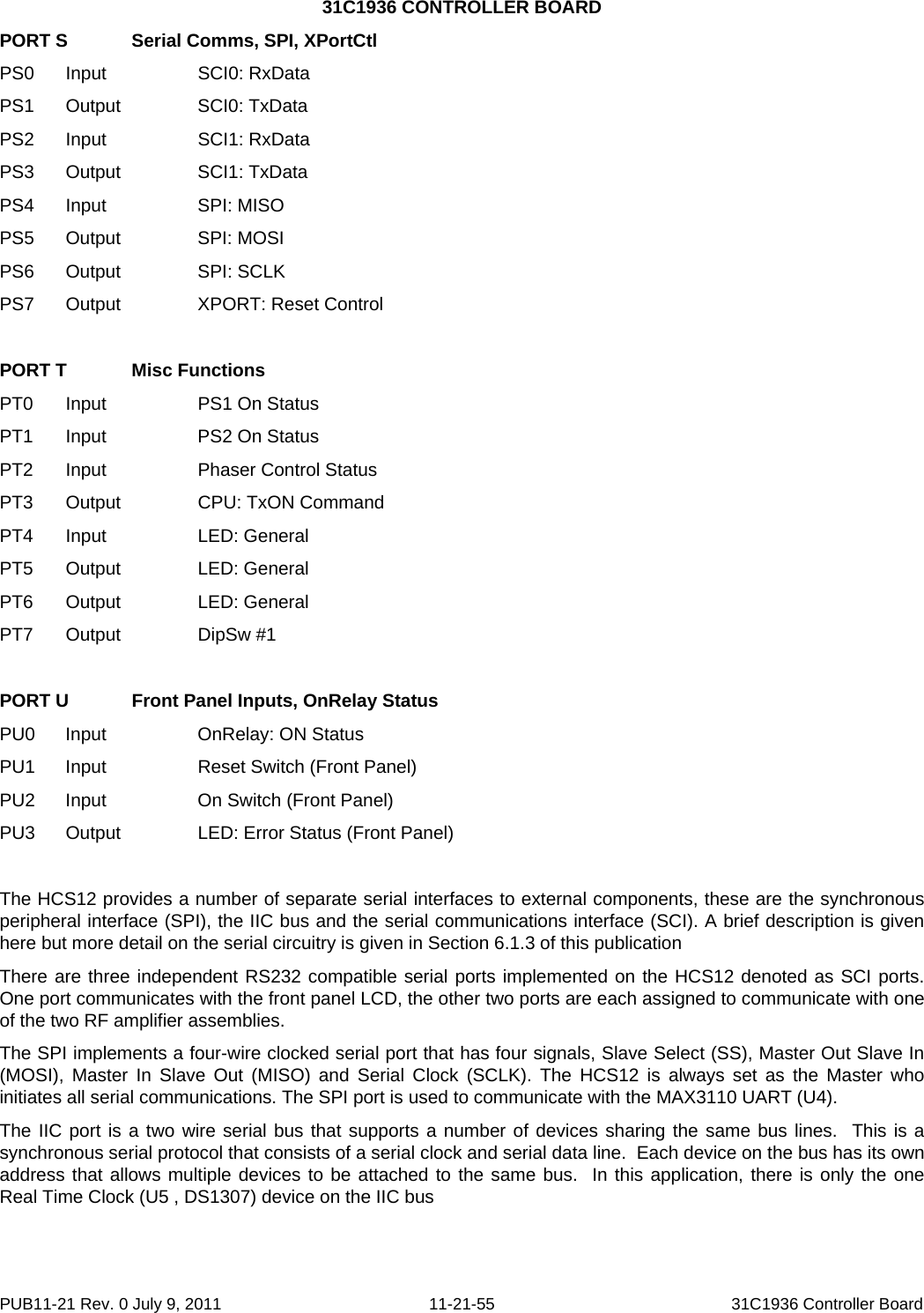
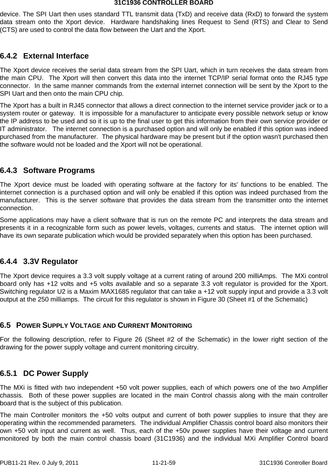
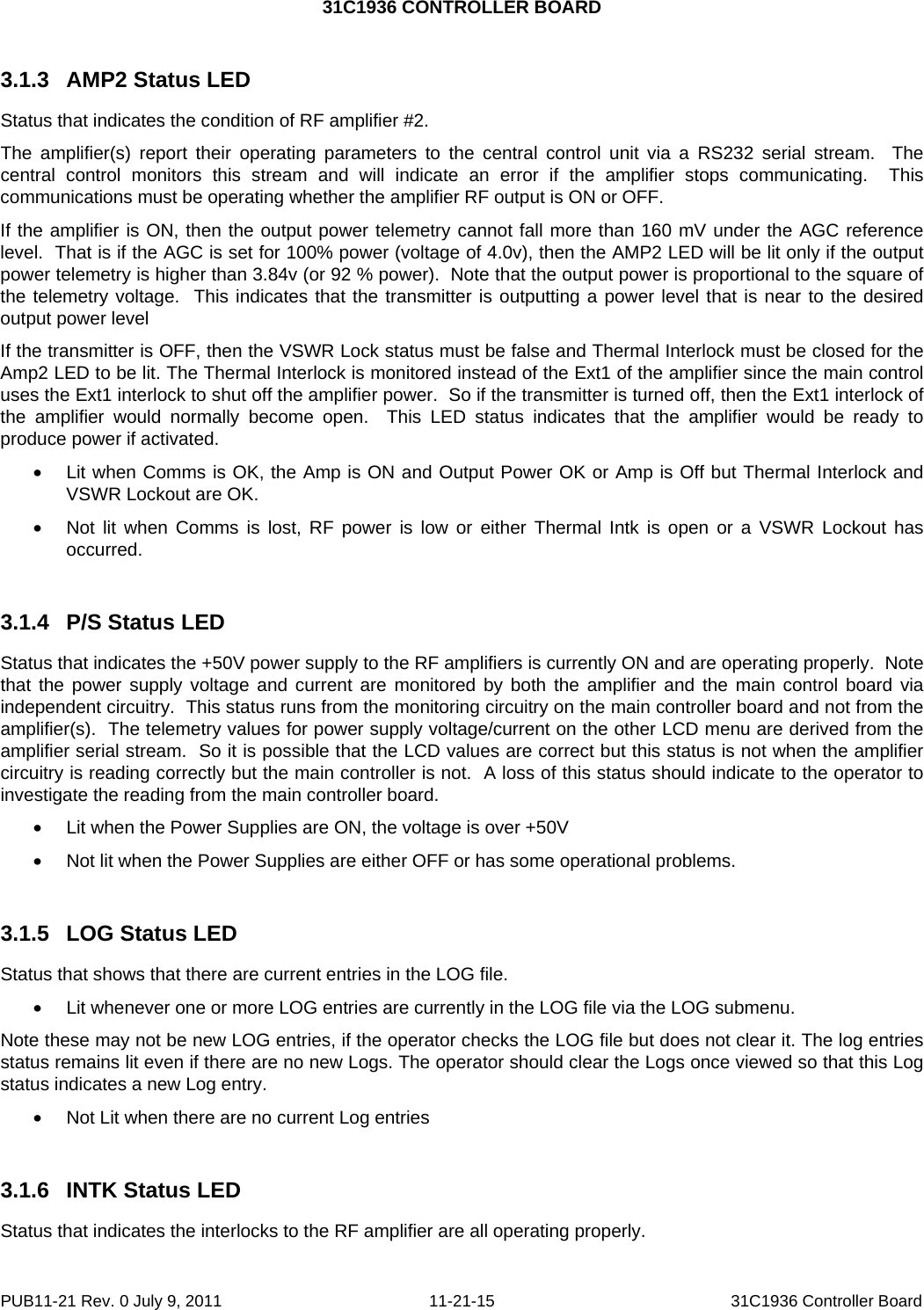
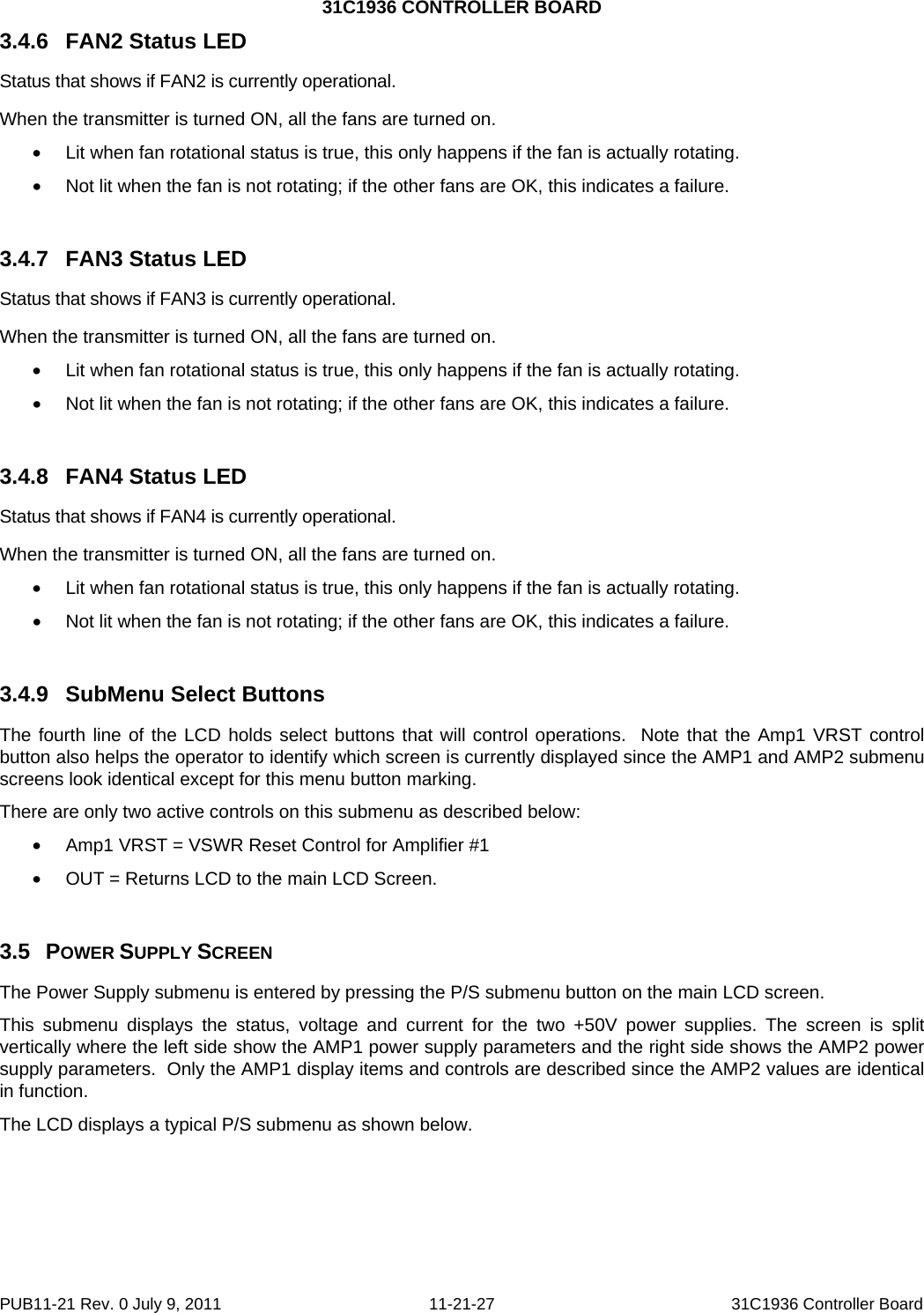
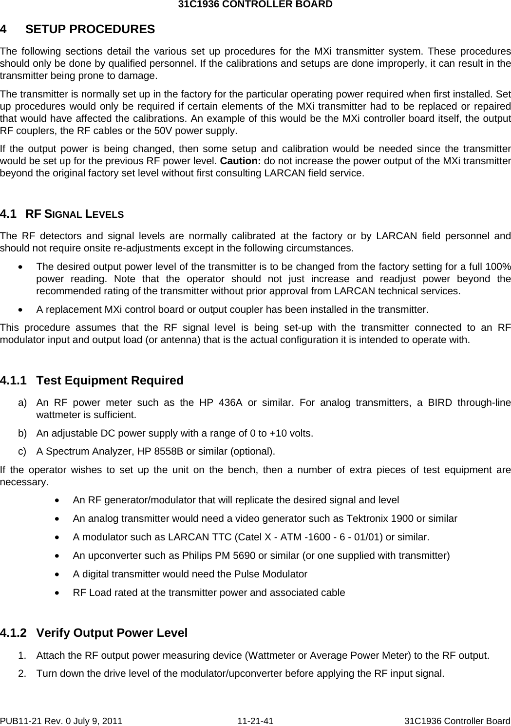
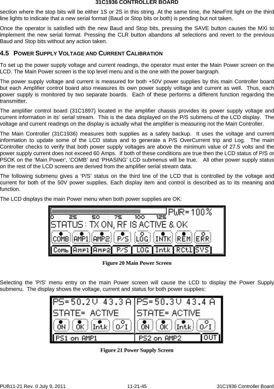
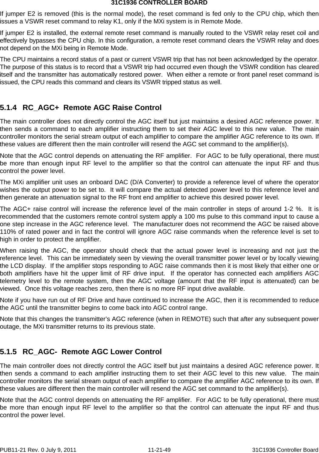
![31C1936 CONTROLLER BOARD 3 3.1 LCD GUI INTERFACE AND TOUCHPAD The user interface to the transmitter is mainly accomplished with the front panel LCD that incorporates a touchpad as an integral part of the unit. The touchpad consists of a thin membrane attached to the LCD surface which implements a software-driven menu selection system. The LCD has the capability of displaying a number of different screens, which are selected by the operator via the touchpad. Each of the separate display screens (called Menus) is detailed in the following subsections along with their respective touchpad menu options. When the MXi transmitter is first powered on or returns from an AC power outage, the LCD displays a screen [Power Up Screen] that only shows for a few seconds and describes the particular transmitter that this MXi is configured for. The same MXi controller board, LCD and software is used for a number of different transmitter configurations. The one specific Power Up Screen reflects the current transmitter configuration. This same information is available on the General Menu screen described in a later subsection. Note that there are no touchpad menu options on this screen, since it only displays for a few seconds. After these seconds have passed, the MXi proceeds into the Main Menu screen described in the next section. MAIN SCREEN AND TOUCHPAD OPERATIONS The Main Menu screen as shown below gives the operator all of the most pertinent values and status to verify the operation of the transmitter. This screen is the one that is normally left displayed when no maintenance or diagnostic checks are being performed. It is from this Main screen that all of the other submenu screens can be accessed. If the operator has switched to another submenu, it is recommended that the LCD is returned to the Main screen, since this shows an overview of the system operation. Figure 5 Main Menu Screen The Main screen can be subdivided into four distinct sections, the main forward RF power at the top line, the transmitter status on the second line, the individual subsystem status on the third line and the submenu options on the fourth and last line. The first line shows the forward RF power that the transmitter is currently generating. This is the power that is actually being sent out to the antenna or system load. There are two elements that show the same information but in different formats. The bar graph gives a graphic display of the RF power output level and is calibrated for 100% at the transmitter’s rated output power. The bar graph will display up to 125% but it is not recommended that the operator increase the power beyond the rated power without prior approval from LARCAN field service. When the power exceeds 110%, the bar graph becomes more solid and darker in the area above 110% to indicate that an overpower condition is present. The same information is provided to the left of the bar graph in a three-digit display, which shows the current power output. When calibrating or setting up the transmitter, this three-digit display value should be used as a reference for the current transmitter power (not the bar graph). This display has a maximum value of 169% power when the transmitter detectors are set up for a DC output of 4.0 at full power. This value is derived from the fact that the detector can output a maximum of 5.0VDC to the telemetry circuits, which translates to an output power of 169%. Of course, this is a maximum display value on the LCD fixed by circuit constraints and the operator should never be approaching this type of power level with the transmitter. If a display of 169% is indeed shown, then either there is a problem with the detector or the power of the transmitter is in fact exceeding 169% and should be attended to immediately. PUB11-21 Rev. 0 July 9, 2011 11-21-13 31C1936 Controller Board](https://usermanual.wiki/Larcan/MXI1002U.Amplifier-Control-PUB/User-Guide-1708509-Page-17.png)
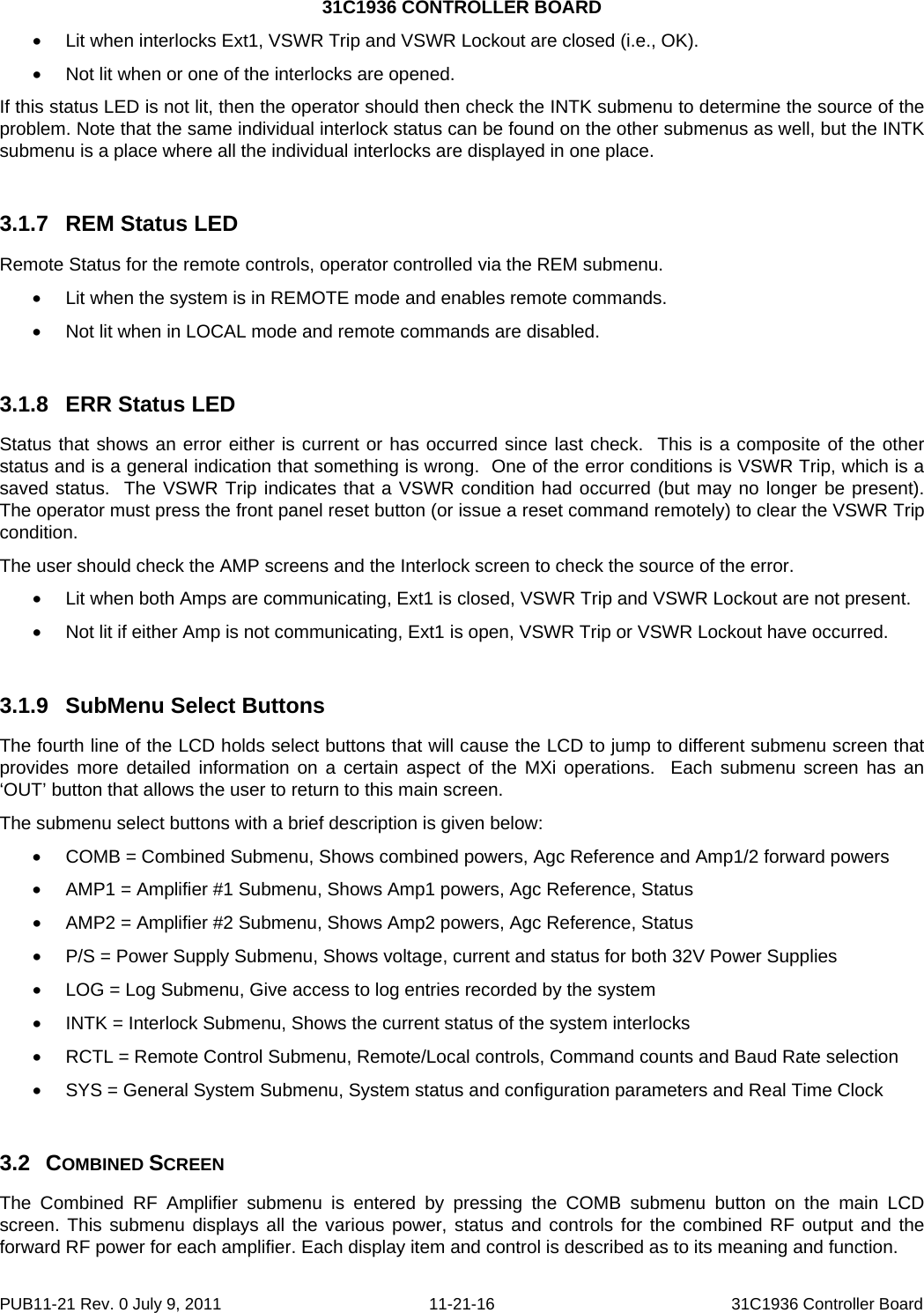
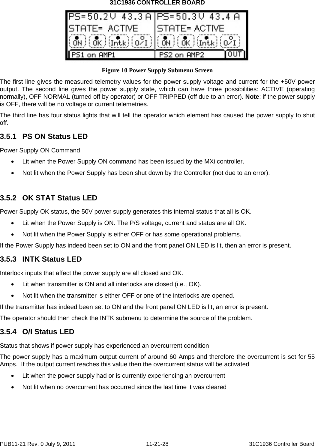
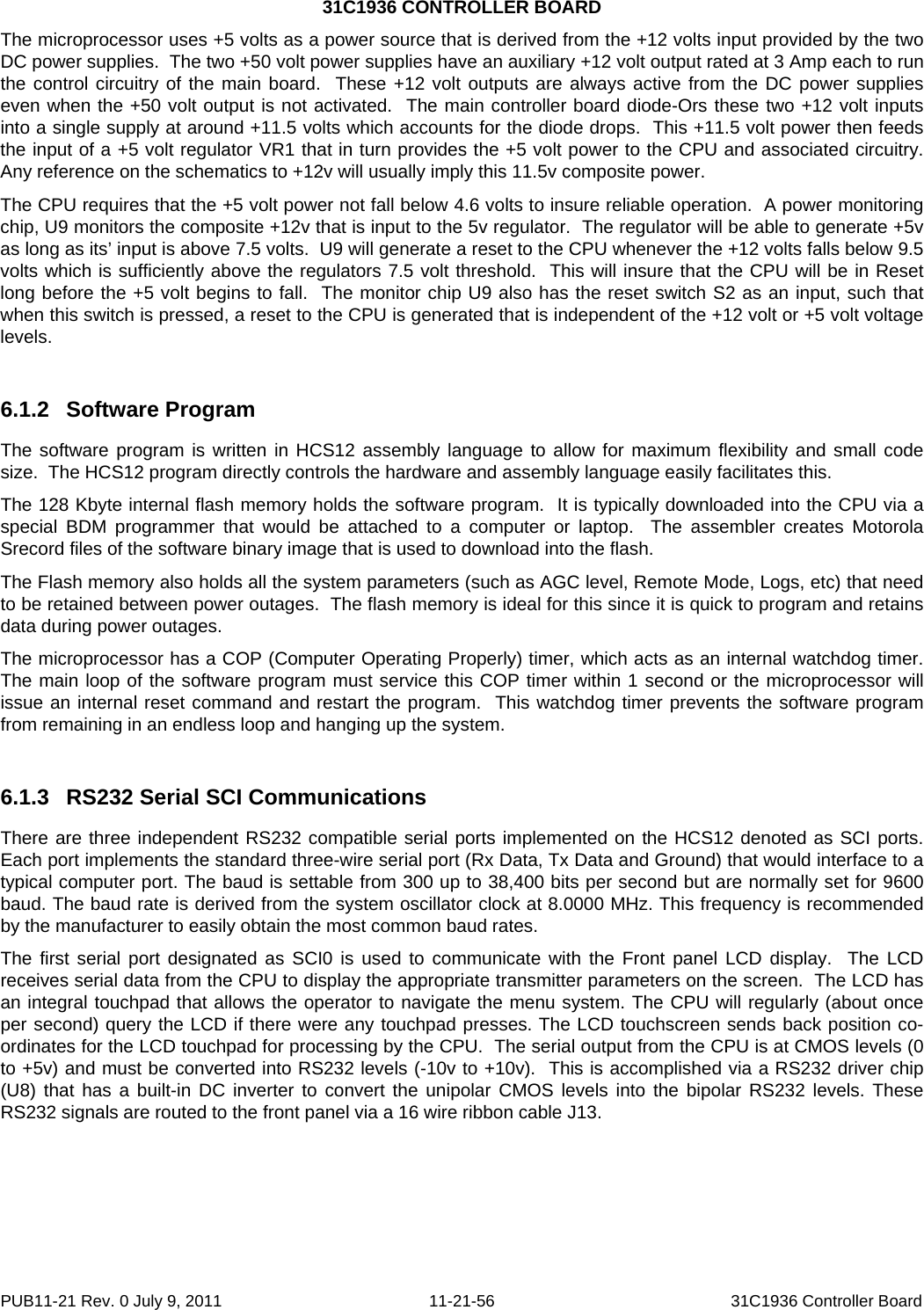
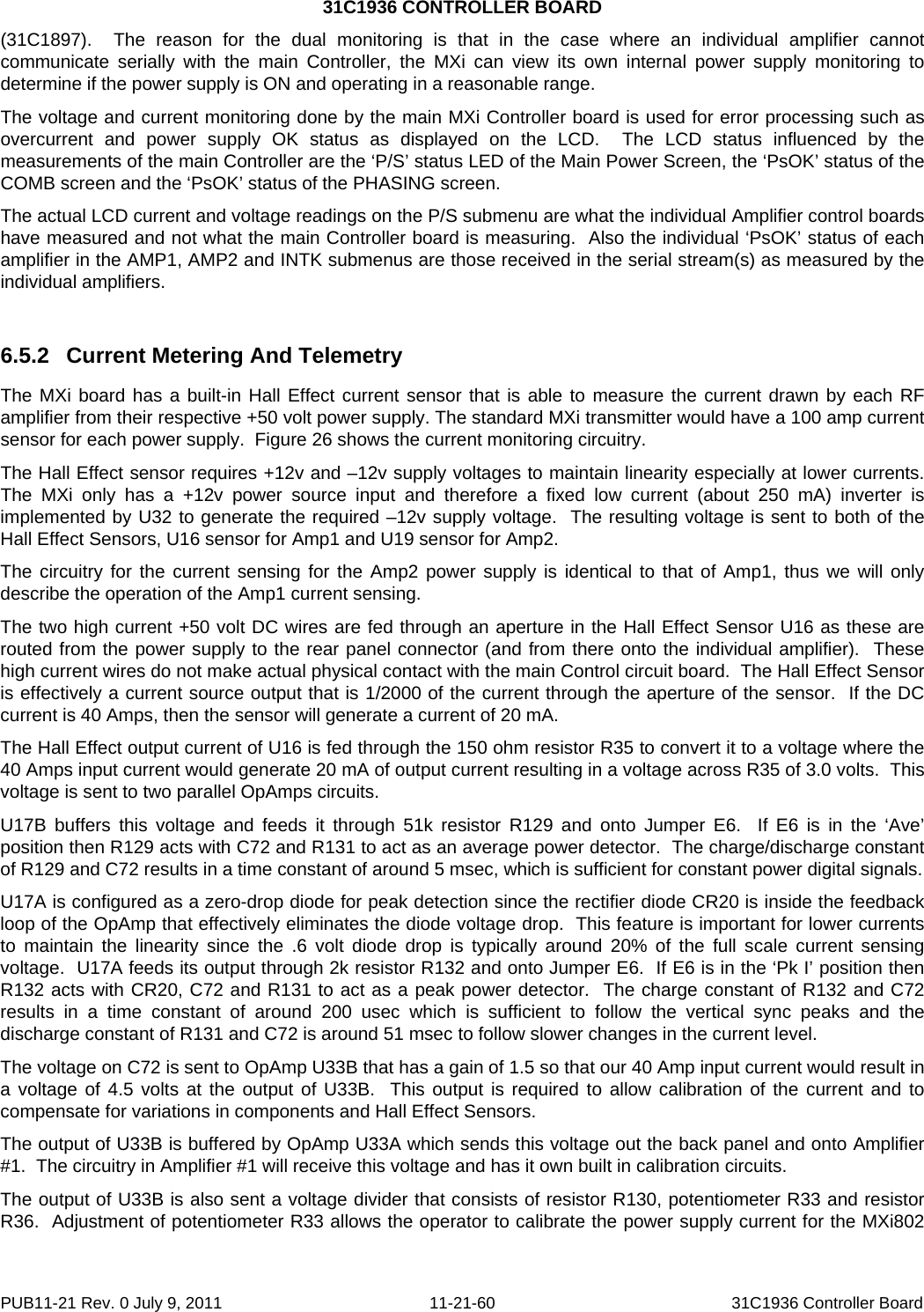
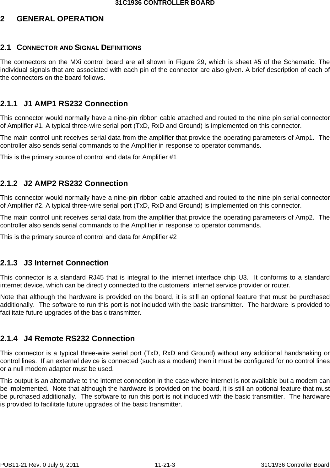
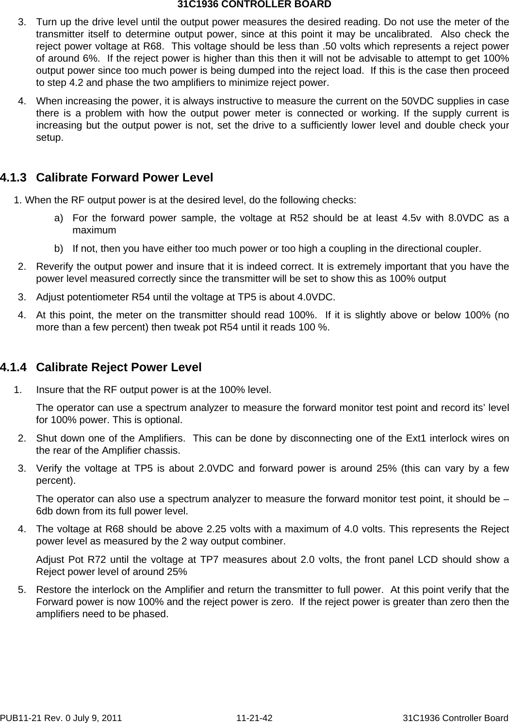
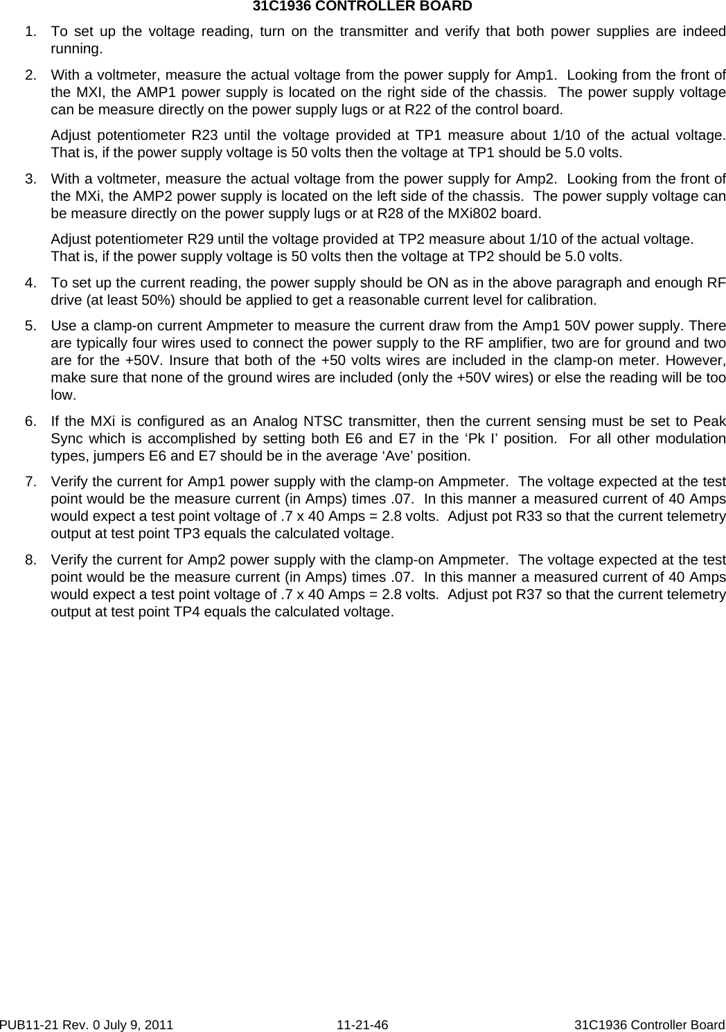
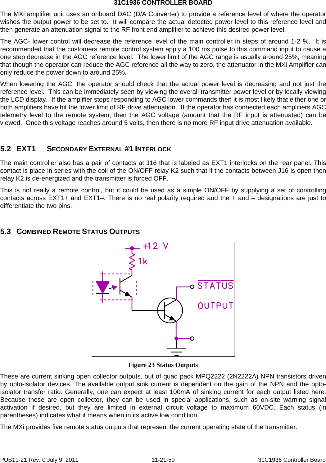
![31C1936 CONTROLLER BOARD 3.5.5 3.6 SubMenu Select Buttons The fourth line of the LCD has a label ‘PS1 on AMP1’ and ‘PS2 on AMP2’ that has no control function but is only displayed to indicate which values are associated with PS1 and PS2. There is only one menu button selection for the Power supply menu and that is the rightmost button labeled OUT which exits this submenu. When the operator is finished in the submenu, an OUT command returns to the Main LCD screen. • OUT = Returns LCD to the main LCD Screen. LOGS SCREEN The LOGS submenu is entered by pressing the LOGS submenu button on the main LCD screen. This submenu begins by displaying the first three log entries that are stored in the internal log table. If there are fewer than three entries, only those one or two log entries are displayed. The first three lines of the display are used to display log entries and the last line is used for menu button options. The LCD displays a typical LOGS submenu as follows: Figure 11 Logs Submenu Screen The logs are displayed up to three at a time, in the order in which they were detected in the controller. That is, the logs are in chronological order from the time they were received. The seventh menu button on the fourth line of the LCD shows the total number of log entries [our example shows entries #=01]. A maximum of 99 log entries can be held in the log table. If the log table already contains 99 entries and a new log has occurred, the oldest log is discarded and the new log is entered into the table. In this manner the log table will hold the 99 most recent logs. In the fourth menu button line of the LCD, the first four button selections (from the left side) allow the operator to navigate through the log table when there are more than three logs. If there are three logs or less, all the entries are already displayed on the LCD. The first menu button is labeled 1ST and causes the display to return to the beginning of the log table and display the first three entries. The second menu button is labeled LAST and causes the display to jump to the end of the log table and display the last three entries. The third menu button is labeled NEXT and causes the display to scroll down one log entry. If the LCD was displaying LOGS 2-4, then pressing NEXT displays LOGS 3-5. The fourth menu button is labeled PREV and causes the display to scroll up one log entry. If the LCD was displaying LOGS 2-4, then pressing PREV displays LOGS 1-3. The fifth menu button is labeled CLR and causes the log table to be cleared and the LCD will have no logs to display and the count will revert back to zero #=00. As noted previously, the log count is located in the seventh menu button position. Pressing this button does not perform any function. The eighth menu button is labeled OUT and causes the LCD screen to return to the Main Menu. PUB11-21 Rev. 0 July 9, 2011 11-21-29 31C1936 Controller Board](https://usermanual.wiki/Larcan/MXI1002U.Amplifier-Control-PUB/User-Guide-1708509-Page-33.png)
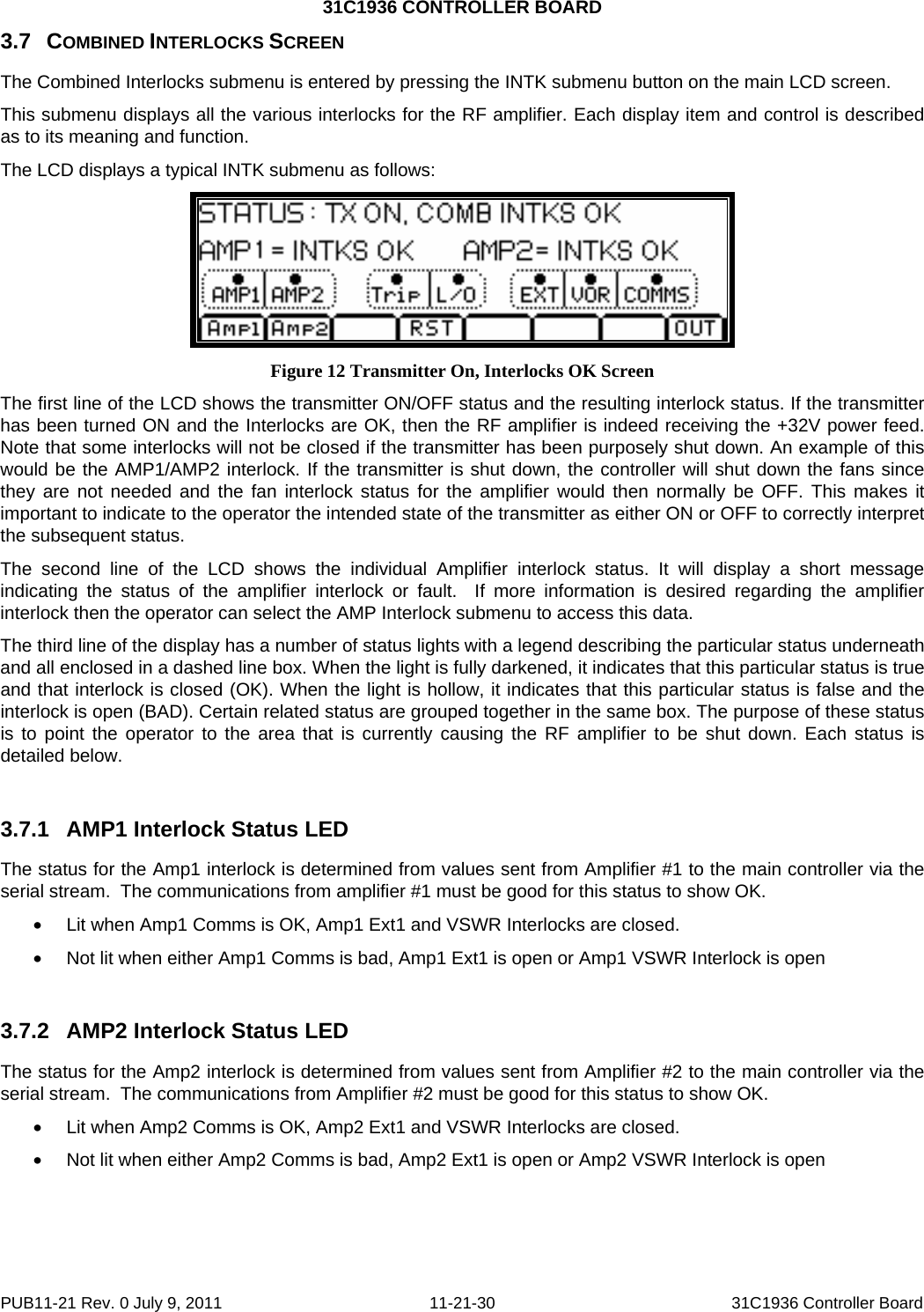
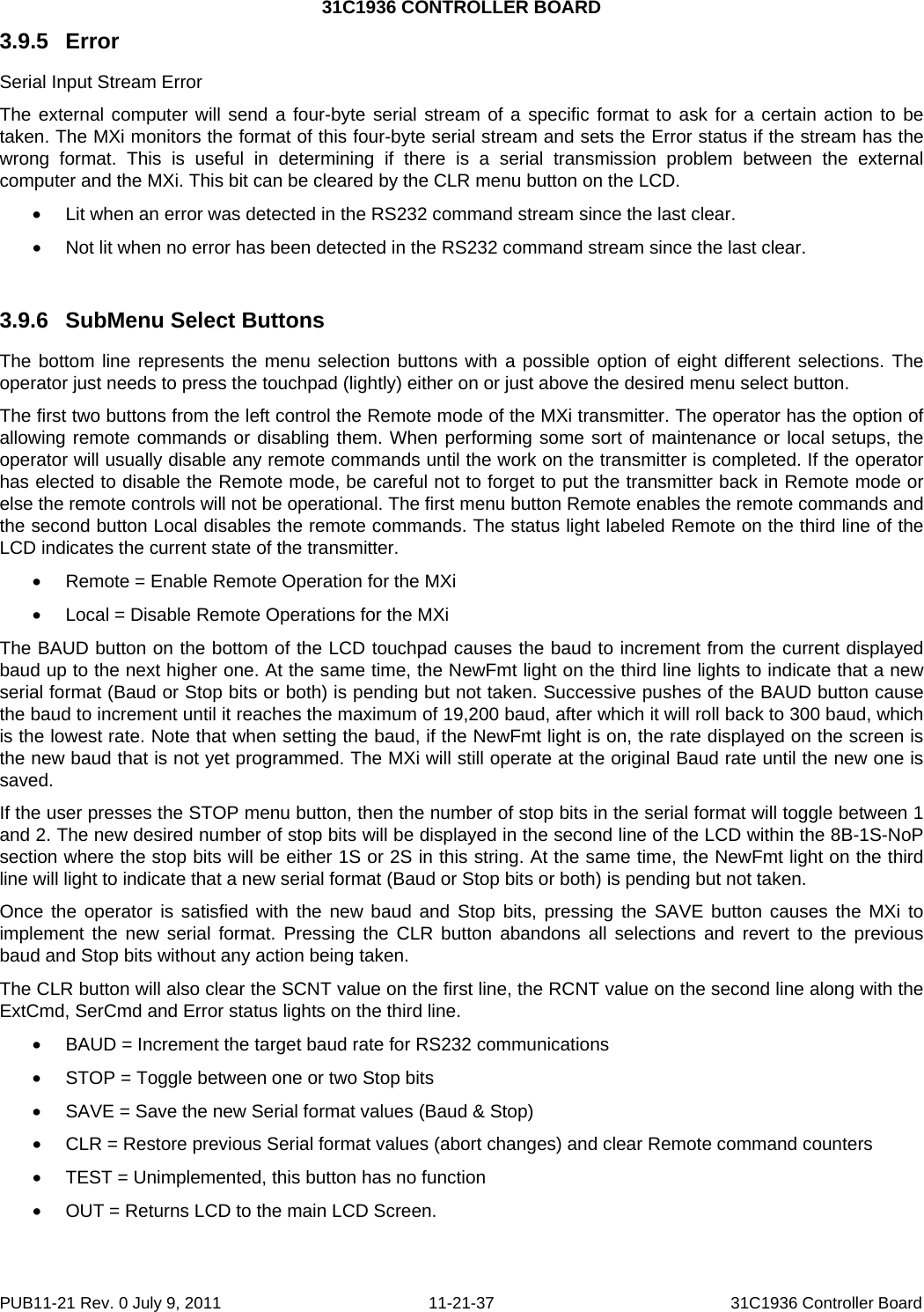
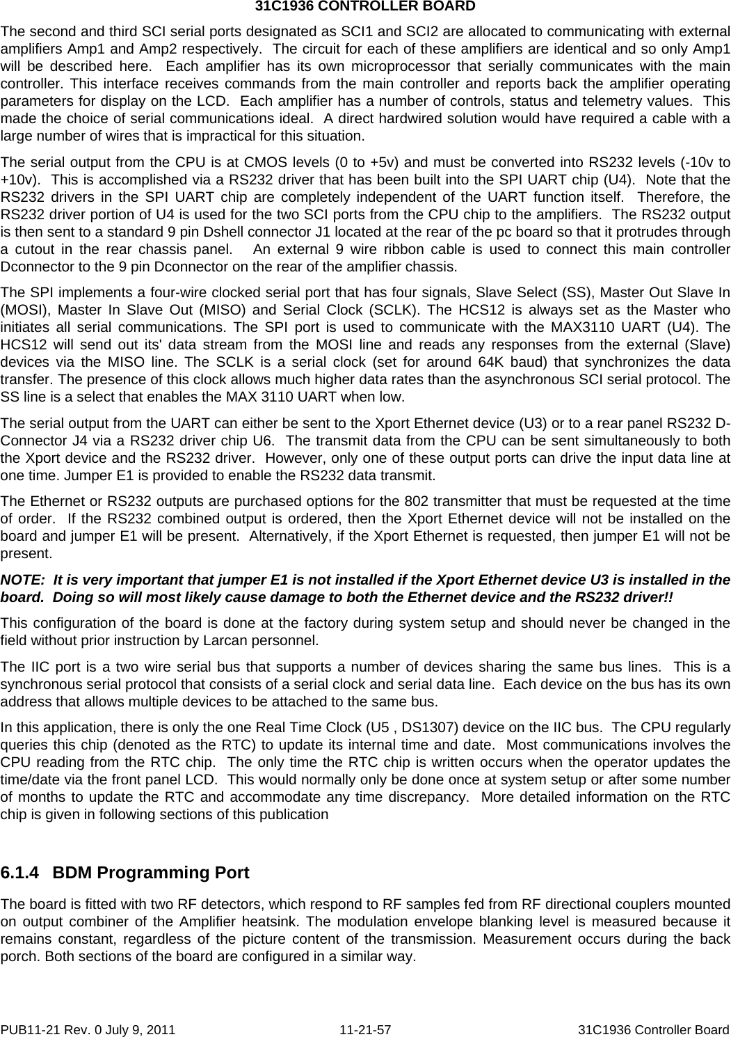
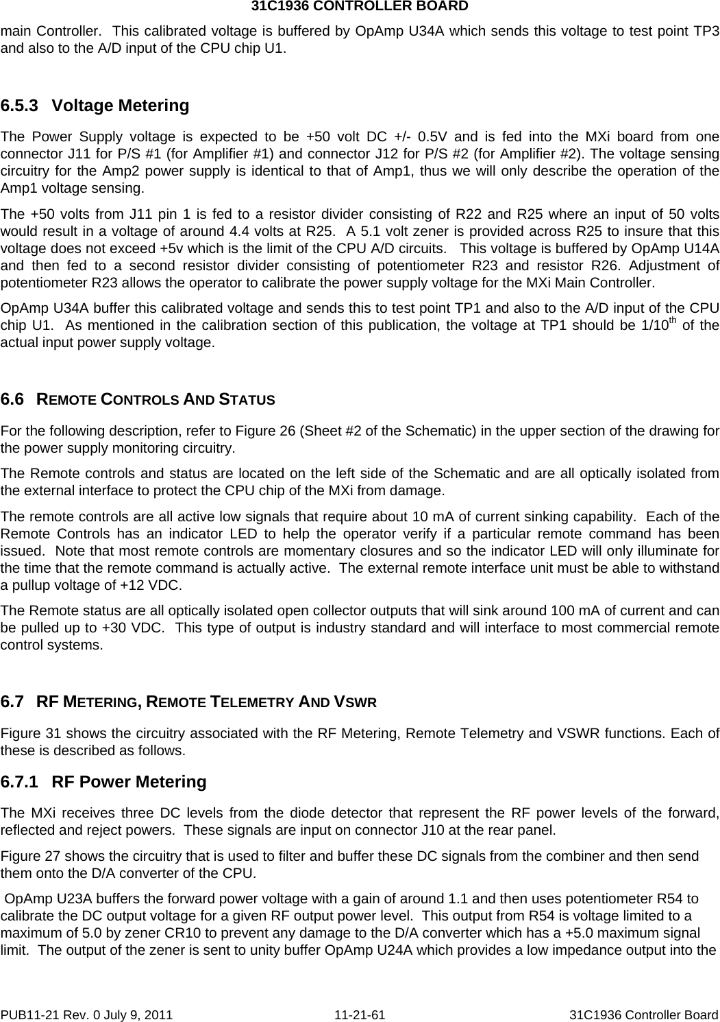
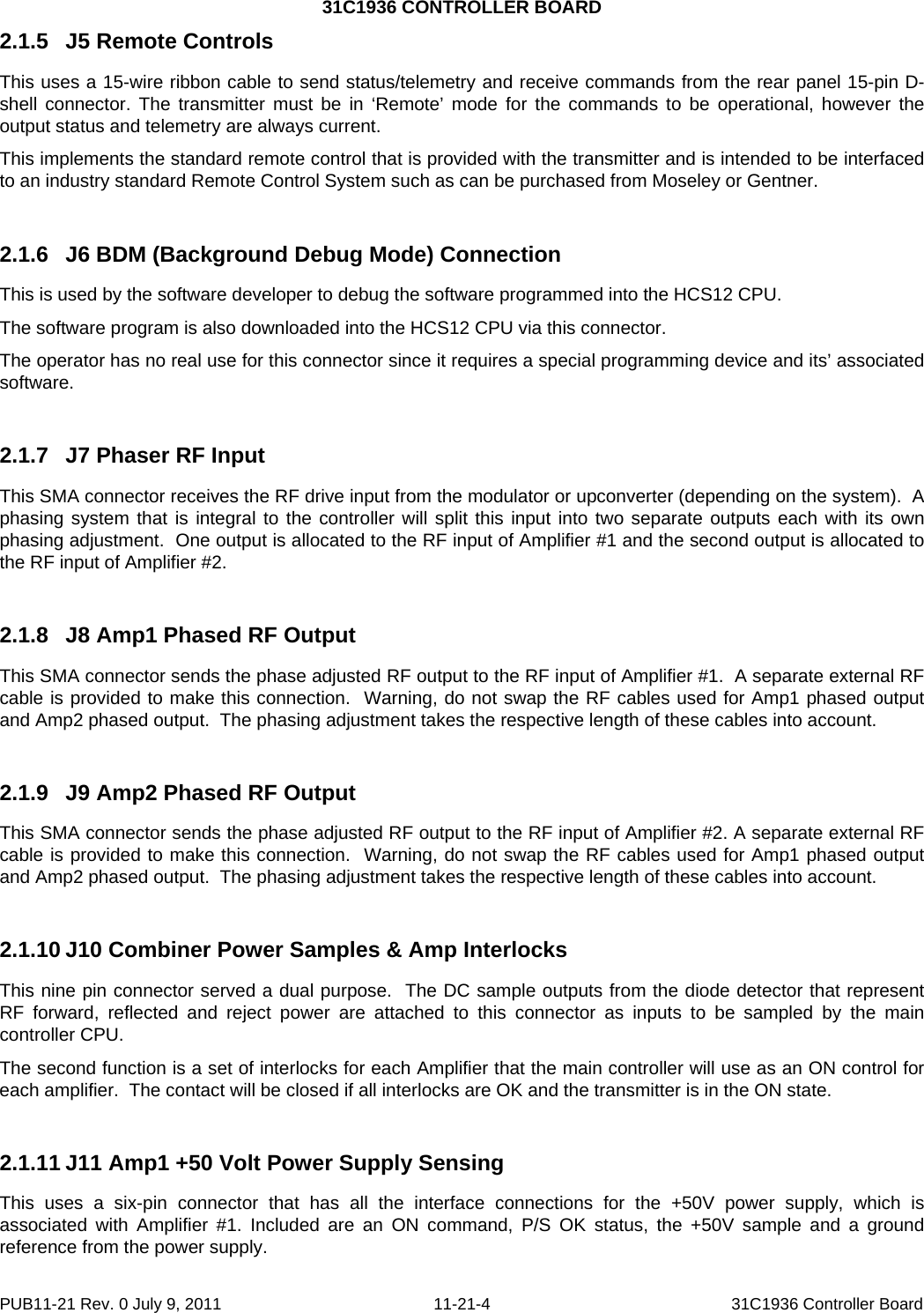
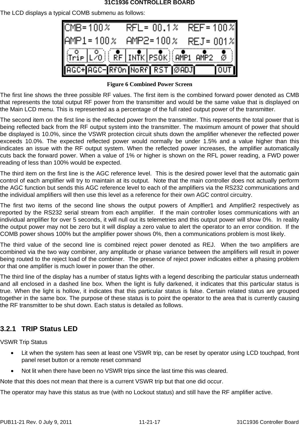
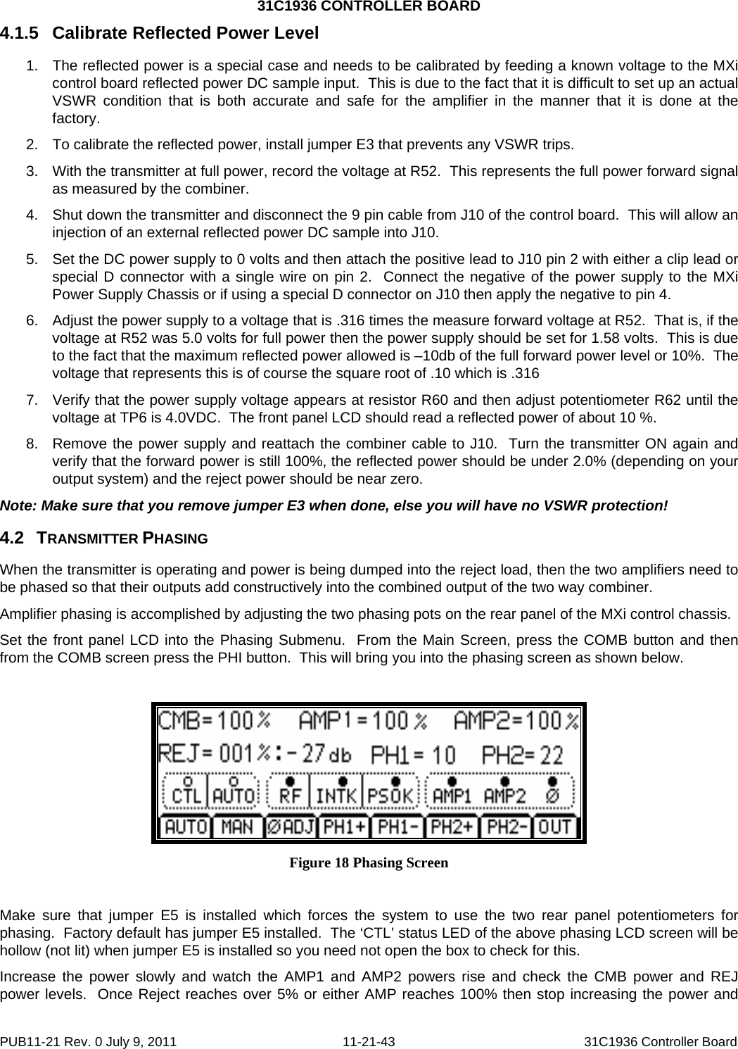
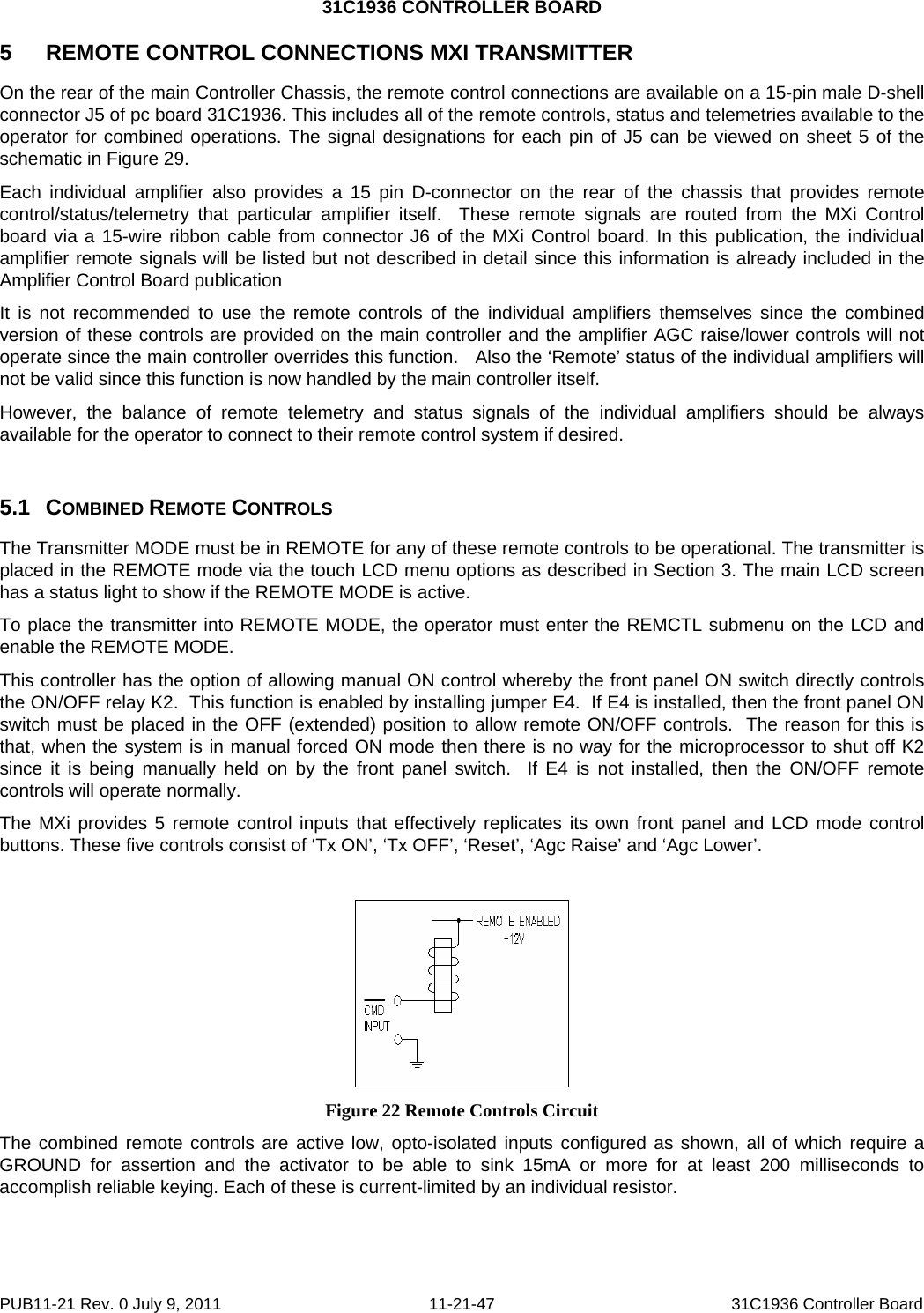
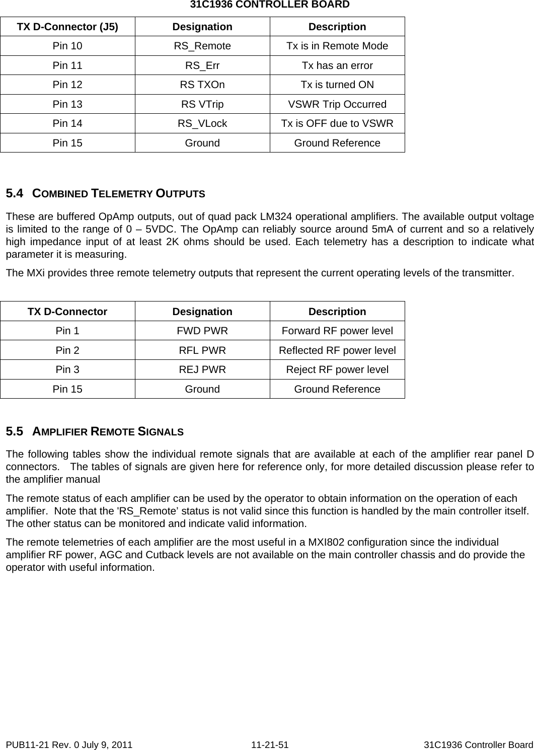
![31C1936 CONTROLLER BOARD • Inet On = Internet interface is active and will respond to external requests [factory setting] • NewIP = Operator has changed (but not yet saved) and new IP address • NewMask = Operator has changed (but not yet saved) and new IP Mask address • Active = The internet is currently receiving or transmitting data • RxD = Data is being received • TxD = Data is being transmitted 3.11.1 SubMenu Select Buttons The bottom line represents the menu selection buttons with a possible option of eight different selections. The operator just needs to press the touchpad (lightly) either on or just above the desired menu select button. The first seven buttons are involved in setting the Internet address and Mask Addresses. Each of these addresses are divided into four sections of three digits each. The operator can increment each of these three digit numbers separately and then move on to the next set if required. Once completed the new values can be saved. Figure 17 Internet SetUp Submenu Screen • SetIP = Set a new IP address, Moves cursor to the first 3 digit number (100 in this case) • Mask = Set a new IP Mask address, Moves cursor to the first 3 digit number (255 in this case) • INC+ = Increment the current IP or IP Mask number, If current number is 100 then go to 101 • NEXT = Move to the next 3 digit IP number, If at the last digits then nothing is done • PREV= Move to the previous 3 digit IP number, If at the first digits then nothing is done • SAVE = Save the new IP or IP MASK address • CLR = Restore the default IP addresses and discard any changes made • OUT = Returns LCD to the System Submenu LCD Screen. PUB11-21 Rev. 0 July 9, 2011 11-21-40 31C1936 Controller Board](https://usermanual.wiki/Larcan/MXI1002U.Amplifier-Control-PUB/User-Guide-1708509-Page-44.png)
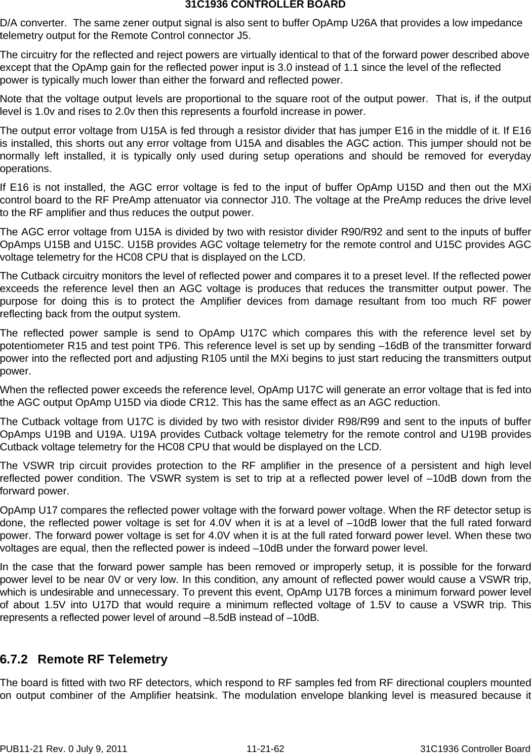
![31C1936 CONTROLLER BOARD PAD13 Output Remote Status: Tx ON PAD14 Output Remote Status: VSWR Trip PAD15 Output Remote Status: Remote Mode PORT E Misc Functions PE0 Input Remote Control: TxOn Command PE1 Input IRQ: From Spi UART PE4 Output LED: Phaser Adjusted PE7 Input Crystal Select [fixed] PORT M Serial Comms, DAC, I/O PM0 Output DAC0: Phaser #2 Control PM1 Output DAC1: Phaser #1 Control PM3 Output PHASER: Control Select PM4 Input SCI2: RxData PM5 Output SCI2: TxData PM6 Input/Output IIC: Data PM7 Output IIC: Clock PORT P Misc Functions PP0 Input Amp2 PsON Status PP1 Input Amp2 PsON Status PP2 Input Spare (E9 is unused) PP3 Input VSWR Trip Status PP4 Output VSWR Reset Control PP5 Input Ext1 Intk Status PORT Q DIP Switch PQ0 Input DipSw #2 PQ1 Input DipSw #3 PQ2 Input DipSw #4 PQ3 Input DipSw #5 PQ4 Input DipSw #6 PQ5 Input DipSw #7 PQ6 Input DipSw #8 PUB11-21 Rev. 0 July 9, 2011 11-21-54 31C1936 Controller Board](https://usermanual.wiki/Larcan/MXI1002U.Amplifier-Control-PUB/User-Guide-1708509-Page-58.png)