Larcan MXI1503U Television Broadcast Translator User Manual splitter
Larcan Inc Television Broadcast Translator splitter
Larcan >
Contents
splitter
41D2355 4-WAY SPLITTER UHF
PUB13-01 Rev 0 Mar 4, 2013 i
CONTENTS
1 GENERAL INFORMATION...........................................................................................................................................2
2 INPUTS AND OUTPUTS.................................................................................................................................................3
3 FRONT PANEL STATUS MONITORING....................................................................................................................5
4 DIGITAL FWD, RFL AND REJECT RF DETECTORS..............................................................................................6
4.1 CALIBRATION ...............................................................................................................................................................7
4.2 TROUBLESHOOTING......................................................................................................................................................7
5 ANALOG INTERNALLY DIPLEXED FWD, RFL AND AURAL RF DETECTORS..............................................8
5.1 CIRCUIT DESCRIPTION ..................................................................................................................................................8
5.1.1 J18 Channel – Visual Forward............................................................................................................................8
5.1.2 J18 Channel – Aural Forward.............................................................................................................................9
5.1.3 J19 Channel – Reflected ......................................................................................................................................9
5.1.4 Test and Calibration..........................................................................................................................................10
TEST EQUIPMENT....................................................................................................................................................................10
5.2 TEST PROCEDURE .......................................................................................................................................................11
6 AMPLIFIER BALANCE ALIGNMENT......................................................................................................................12
7 SPECIFICATION............................................................................................................................................................13
8 AMPLIFIERS TEST.........................................................................................................................................................1
LIST OF FIGURES
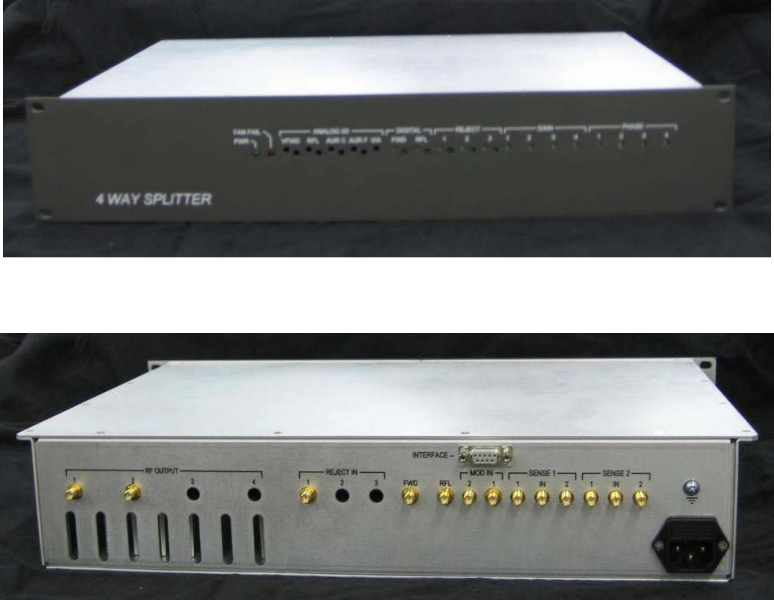
FIGURE 1 4 WAY SPLITTER FRONT AND REAR VIEW ....................................................................................................................3
FIGURE 2 4-WAY SPLITTER RF FLOW DIAGRAM 21B2917S1 SHT1 REV 0...................................................................................4
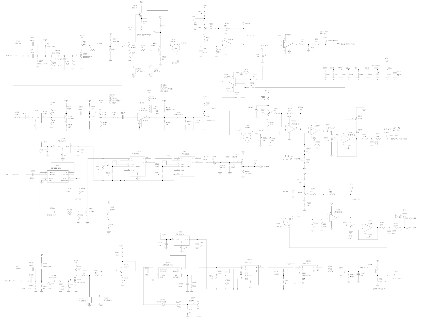
FIGURE 3 4-WAY SPLITTER UHF SCHEMATIC 41D2355S1 REV 0 ................................................................................................5
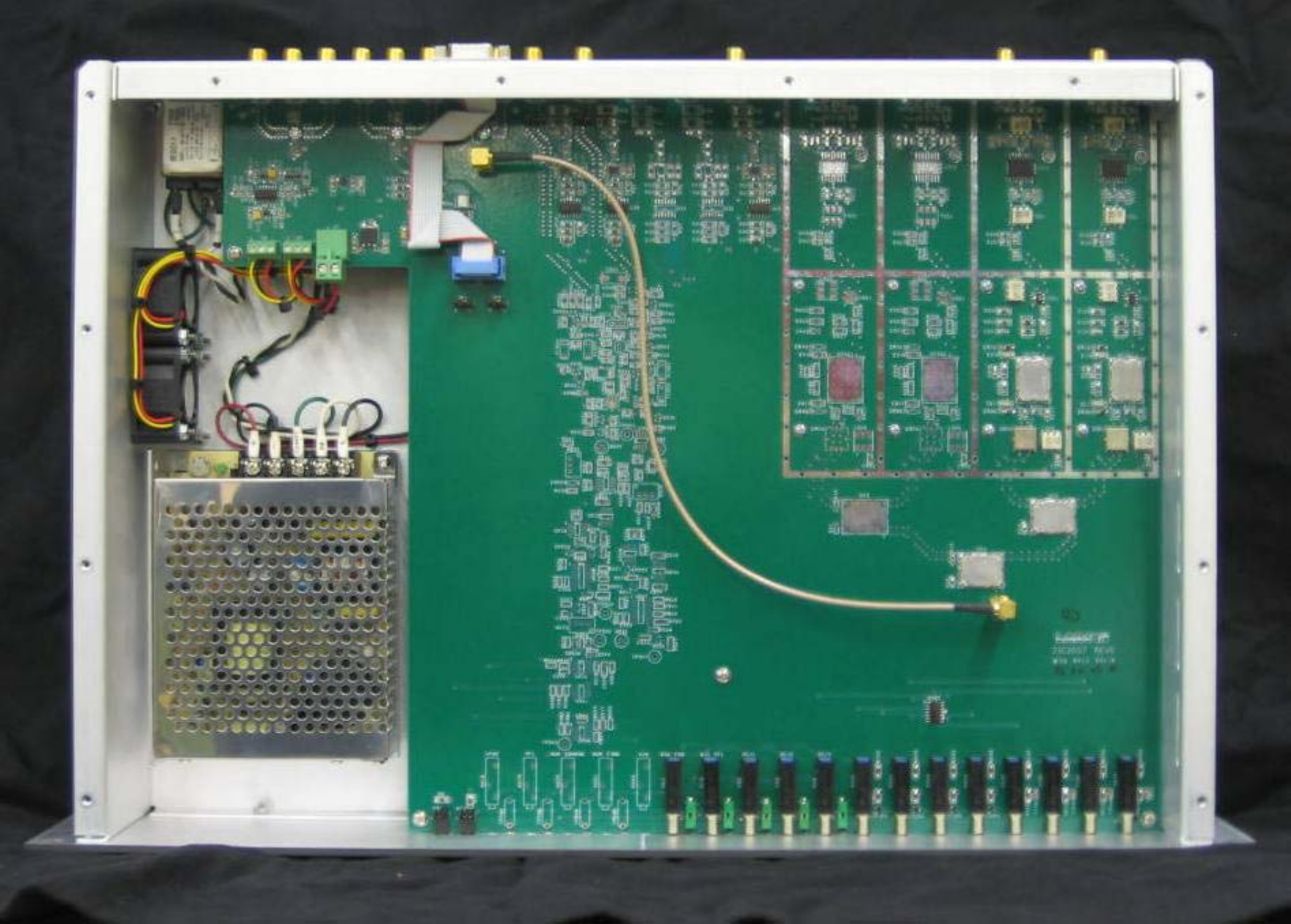
FIGURE 4 4-WAY SPLITTER ASSEMBLY ........................................................................................................................................6
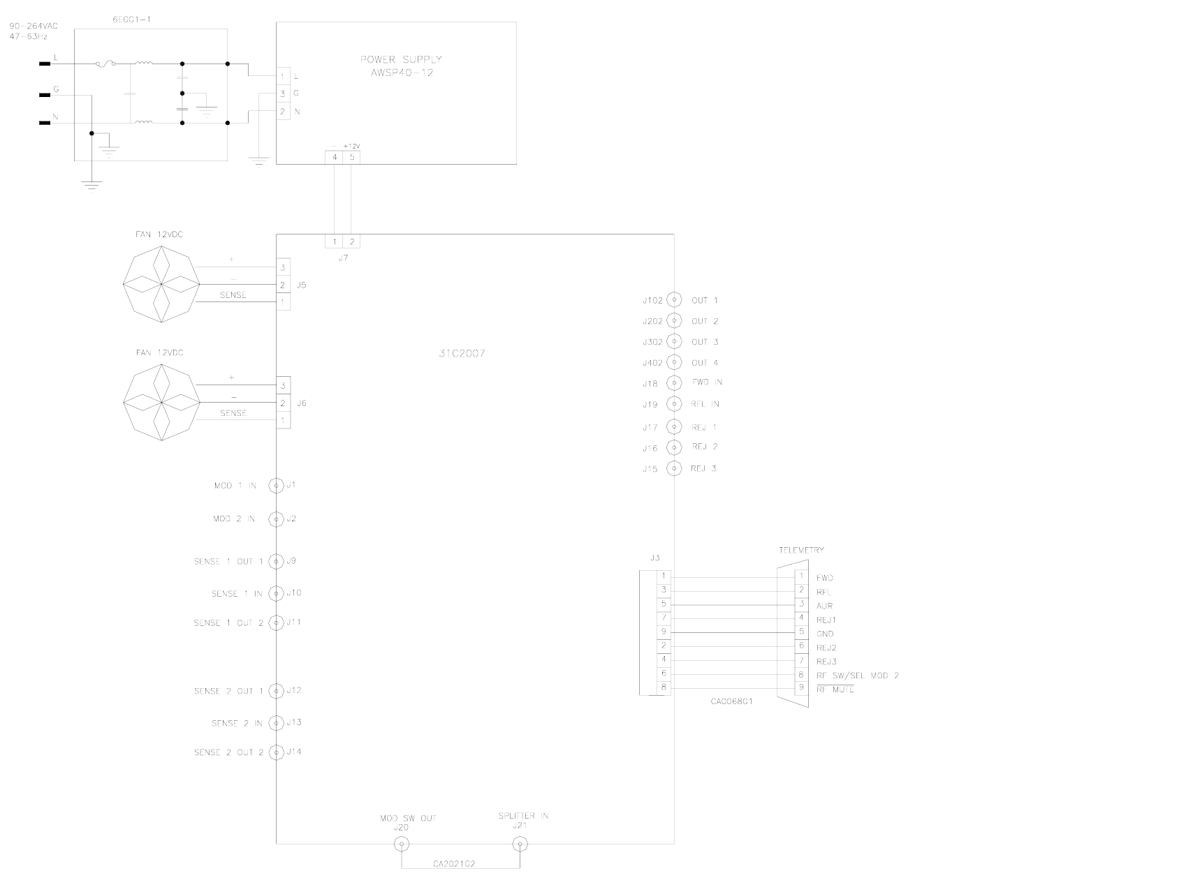
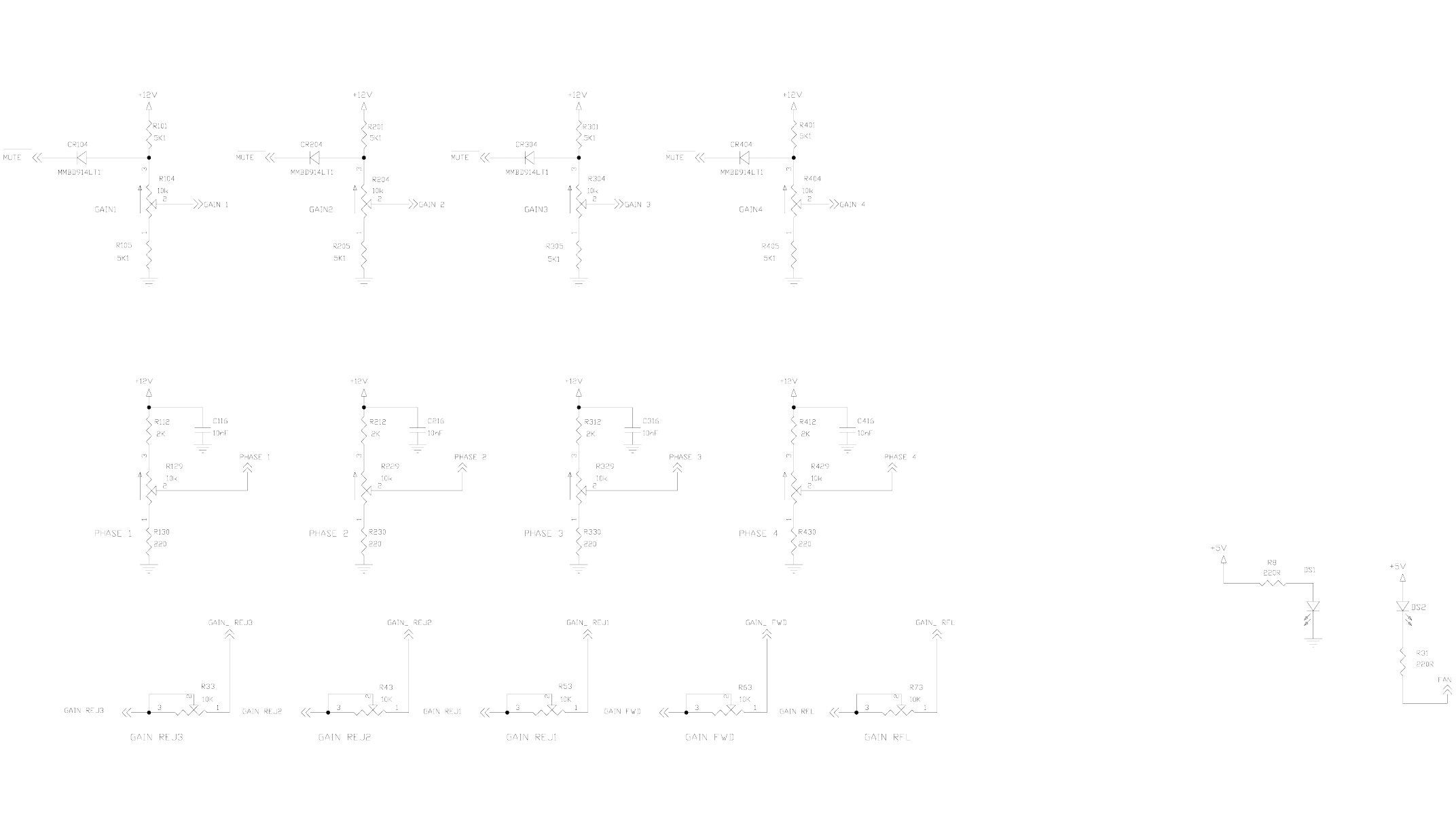
FIGURE 5 4-WAY SPLITTER PCB SCHEMATIC 31C2007S1 SHT 1 REV 0 .......................................................................................7
FIGURE 6 4-WAY SPLITTER PCB SCHEMATIC 31C2007S1 SHT 2 REV 0 .......................................................................................8
FIGURE 7 4-WAY SPLITTER PCB SCHEMATIC 31C2007S1 SHT 3 REV 0 .......................................................................................9
FIGURE 8 4-WAY SPLITTER PCB SCHEMATIC 31C2007S1 SHT 4 REV 0 .....................................................................................10
FIGURE 9 4-WAY SPLITTER PCB SCHEMATIC 31C2007S1 SHT 5 REV 0 .....................................................................................11
FIGURE 10 4-WAY SPLITTER PCB SCHEMATIC 31C2007S1 SHT 6 REV 0 ...................................................................................12
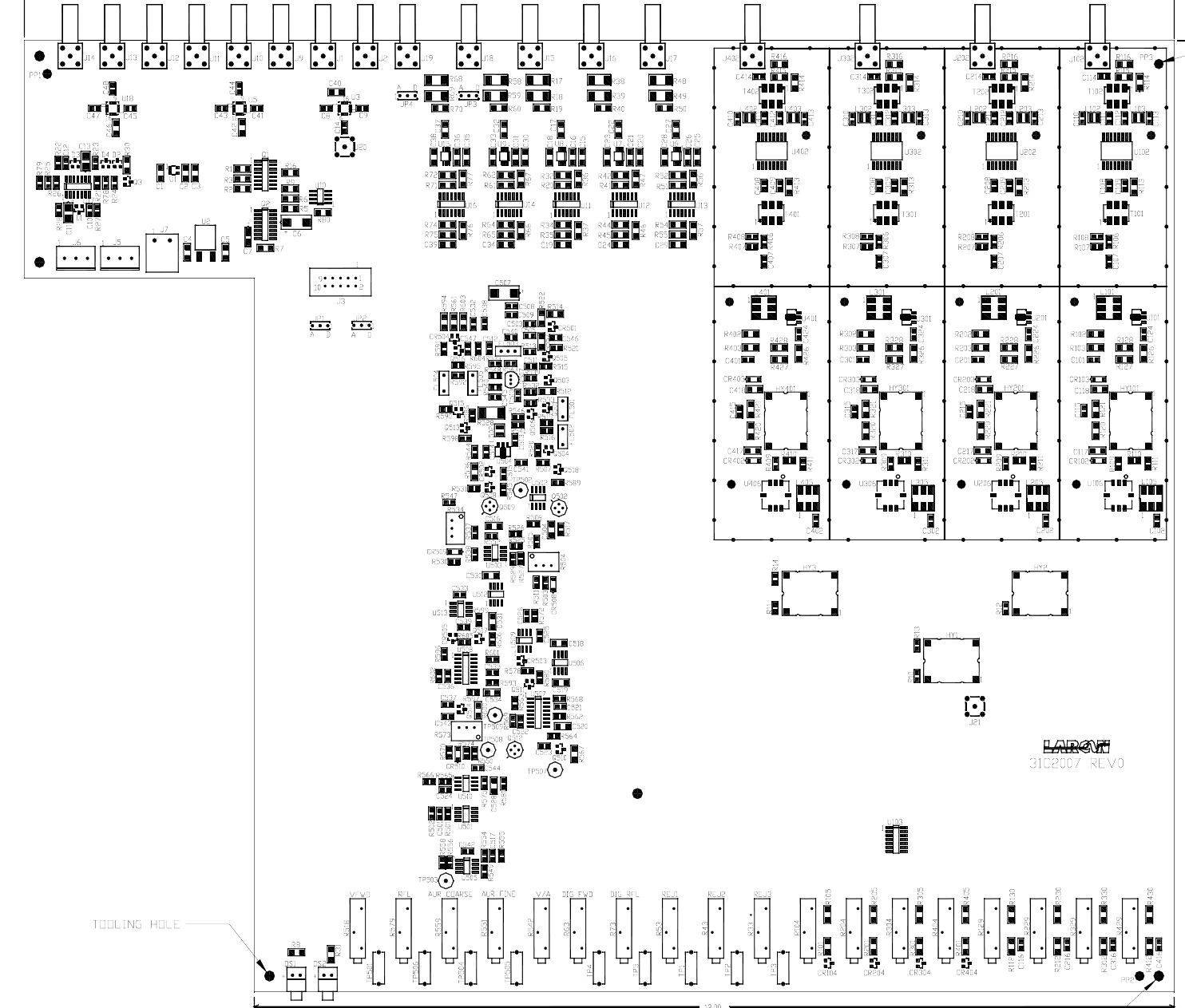
FIGURE 11 4-WAY SPLITTER PCB ASSEMBLY 31C2007A1 SHT 1 REV 0....................................................................................13
41D2355 4-WAY SPLITTER UHF
PUB13-01 Rev 0 Mar 4, 2013 2
1 GENERAL INFORMATION
The Splitter is an intermediate RF Amplification stage employed in LARCAN UHF transmitters. A single 4-Way
Splitter can be configured to drive from two to up to four higher power amplifiers. Typically, the signal level applied
to the Splitter from the Modulator is between 0dBm and +5dBm (50 ohms). Every output gain and phase is
adjustable from the front panel.
The +12VDC Power Supply for the Splitter power stages is high efficiency switching supply. Power Supply is rated
for 40W DC output power.
Two 12VDC fans located on the left side panel of Splitter assembly provide enough air flow to cool down all four
HELA10 RF amplifiers and other necessary circuits.
Splitterr has built in three RF switches used for Modulator Switching and switching of RF Sense signals applied to
Modulators for linear and nonlinear correction. +12VDC signal applied to the rear connector TELEMETRY pin 8
named ”RF SW2 ON/SEL MOD2” changes active connection from INPUT 1 to INPUT 2.

41D2355 4-WAY SPLITTER UHF
PUB13-01 Rev 0 Mar 4, 2013 3
2 INPUTS AND OUTPUTS
The 4-Way Splitter requires DC Power, a Control and Monitoring Interface, an RF input drive and an output
connections to a higher power stages. Its inputs and outputs consist of the following:
POWER IN: 2-Pin Connector J7
Pin Function
1 GND
2 +12VDC
AC receptacle 6EGG1-1 has built–in holder for slow blow 2A fuse model 218002.
MOD 1 IN and MOD 2 IN: SMA Connectors (50 ohm)
These are the RF signal inputs to the Splitter. Only one input is used to drive amplifiers at a time. These signals are
received from the Modulator #1 and Modulator #2(if used). If a matched 50-ohm attenuator pad has been installed
at the 4-Way Splitter Input, it must remain installed and must not be removed without first contacting LARCAN
Technical Service. The attenuator, when installed, protects the transmitter’s Power Amplifiers from being
overdriven.
SENSE 1 IN and SENSE 2 IN: SMA Connectors (50 ohm)
These are the RF signal from Mask Filter Input and Mask Filter Output respectively. These signals are switched to
SENSE 1 OUT 1 ans SENSE 2 OUT 1 when MOD 1 IN is selected. These signals are switched to SENSE 1 OUT 2
ans SENSE 2 OUT 2 when MOD 2 IN is selected. Only one input is used to drive amplifiers at a time. These
signals are received from the Modulator #1 and Modulator #2(if used). If a matched 50-ohm attenuator pad has
been installed at the 4-Way Splitter Input, it must remain installed and must not be removed without first contacting
LARCAN Technical Service. The attenuator, when installed, protects the transmitter’s Power Amplifiers from being
overdriven.
RF 1 OUT to RF 4 OUT: SMA Connector (50 ohm)
These are the four RF Outputs from the Splitter.
TELEMETRY: 9-Pin D-subminiature Connector.
Interface with Transmitter Control Unit is provided through this connector: Select Modulator 2 signal, FWD and RFL
telemetry, Aural and Reject 1,2 3 telemetry.
The Splitter can function as an amplifier gain block without the TELEMETRY interface connected to the transmitter’s
controller. This way bench testing of the RF circuits can be performed without connection to a transmitter controller.
The pinout of the Control and Monitoring interface is as follows.

41D2355 4-WAY SPLITTER UHF
PUB13-01 Rev 0 Mar 4, 2013 4
31C2007-J3 PIN TELEMETRY PIN LABEL FUNCTION
1 1 FWD Forward
3 2 RFL Reflected
5 3 AUR Aural
7 4 REJ1 Reject 1
9 5 GND Ground2
2 6 REJ2 Reject 2
4 7 REJ3 Reject 3
6 8 RF SW/SEL MOD 2 +12V Select Modulator 2
8 9 RF MUTE RF Mute (active LOW)
41D2355 4-WAY SPLITTER UHF
PUB13-01 Rev 0 Mar 4, 2013 5
3 FRONT PANEL STATUS MONITORING
The Status of the 4-Way Splitter can be seen at the front panel using two following LED:
POWER (Green) indication. When this LED is on, it indicates that the internal regulator provides +5VDC to the
circuitry. If this LED is off, it means either that the 4-Way Splitter breaker on transmitter AC Distribution Panel is
turned off or that the 4-Way Splitter Power Supply is no longer functioning.
FAN FAILED (Red) indication is monitoring the operation of the internal cooling fans. The illuminated LED
indicates that one or both fans rotation speed is insufficient.

41D2355 4-WAY SPLITTER UHF
PUB13-01 Rev 0 Mar 4, 2013 6
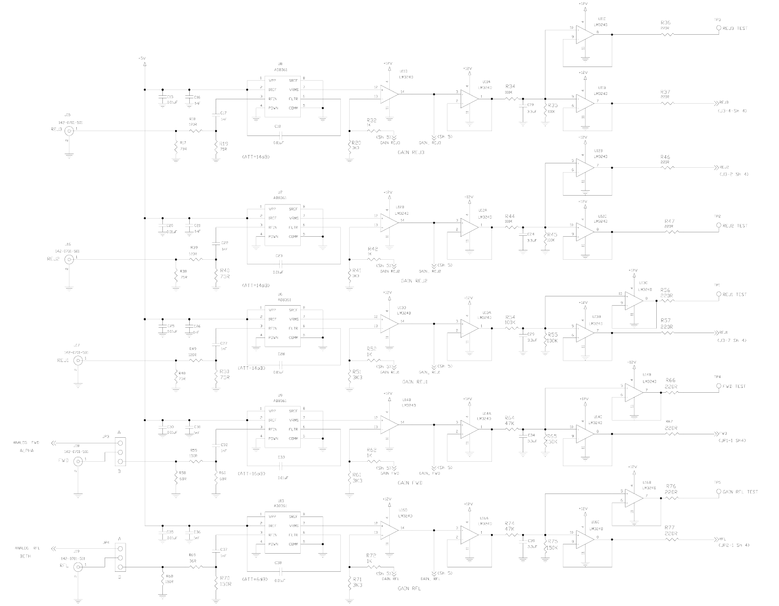
4 DIGITAL FWD, RFL AND REJECT RF DETECTORS
Jumpers JP1, JP2, JP3 and JP4 in D position.
This board has five RMS power detectors that receive RF samples via coaxial cables and translate that level of RF
power into a corresponding DC voltage. There are five similar and independent average RMS RF power detectors
on this board that are useful for measuring digital/reject power. Each of the outputs of the RF detectors have buffer
OpAmps, test points and calibration potentiometers to generate output DC voltages.
This publication only describes the operation of the RF Detector Board itself and does not follow all the specific
signals going out of the board. The Operations publication specific to the transmitter model details the signal flow
between subsystems. This is because different transmitter models have varying signal paths and designations,
even though they all use the same RF Detector Board.
RF signals at J15,J16,J17,J18 and J19 connectors represent reject, forward and reflected powers at different points
of the amplification and combining systems. The RF probe sample levels are set up at the factory for the transmitter
rated power. Any changes to the transmitter power or RF probe depths require a readjustment of the RF detector
level. These connectors are SMA type. The following list gives a brief description of the basic function of each
connector on this board.
J3 is a 10-pin ribbon cable connector arranged as two rows of five pins each. This connector routes all telemetry
signals from the board to TELEMETRY connector on the rear panel.
J18 The expected FWD sample signal at J18 shall have level +20dBm RMS for transmitter operating at full power.
Telemetry output at TP4 will be 4V.
J19 The expected RFL sample signal at J19 shall be as low as possible. The detector board was calibrated to
indicate 10% Reflected power at RF level +10dBm RMS. Telemetry output at TP5 will be 4V. Similarly 1% Reflected
power will be represented by 0.316V at TP5.
J15,J16,J17 The expected RF sample signals at J15,J16,J17 shall be also as low as possible. The RF level
+17dBm RMS represents 100% Rejected power. Telemetry output at TP3,TP2 and TP1 will be 4V.
The circuit topologies for all five detector circuits are identical. Described is the circuit for J18 input when the
detector is used to measure transmitter FWD power. The RF input at nominal +20dBm level is first passed through
a π resistive attenuator 16dB to reduce the input power from +20dBm down to +4dBm at the input of the AD8361 IC
U9. This is done to protect the AD8361 device from excessive RF input power. This low level RF input is then
capacitively coupled via C32 into the device at pin 3 to eliminate any DC component. The AD8361 device does its
rms conversion and generates the DC output voltage at pin 7. An external filter capacitor of .01 uF has been added
between pin 6 and Vpp to lower the corner frequency of the low pass filter and generate a longer averaging time
constant. Capacitors C30 and C31 simply provide bypassing of the +5V supply to the AD8361 device.
DC output from U9 is sent to OpAmp U14D. The gain of U14D is adjustable by front panel potentiometer R63. The
output of the buffer U14A is reduced by resistive divider R64/R65 and lowpass filtered by C34. Finally FWD
telemetry voltage is buffered by U14B nand U14C and applied to TP4 and PCB J3-1 as the telemetry outputs. The
actual adjusted telemetry voltage level can be monitored at front panel test point TP4. The detector gain should be
adjusted to the desired 4.0 volts at test point TP4 by potentiometer R63 placed across the feedback path of U14D.
Note that the representative RF power is related to the square of the voltage such that a voltage reading of 2.0VDC
is not half power but a quarter power (2*2 / 4*4 = 4/16 = ¼ power).
41D2355 4-WAY SPLITTER UHF
PUB13-01 Rev 0 Mar 4, 2013 7
4.1 CALIBRATION
The following steps should be followed when calibrating all five RF detectors:
a) Disable AGC. Verify that the transmitter is at full rated power
b) Apply the TX FWD RF sample to the SMA connector J18 and measure the input voltage into the OpAmp
U14D-12. This level should not exceed 4.7VDC, since the maximum output of U9 is +4.8VDC. Adjust
calibration potentiometer R63 until telemetry test point TP4 measures 4VDC.
c) Disable Transmitter VSWR protection –Cut Back, VSWR Trip and Lockout. Apply the TX FWD RF sample
to the SMA connector J19 (TX RFL RF sample input) trough 10dB in–line attenuator and measure the
input voltage into the OpAmp U16D-12. This way 10dB Return Loss (10% reflected power) is simulated.
This level should not exceed 4.7VDC, since the maximum output of U15 is +4.8VDC. Adjust calibration
potentiometer R73 until telemetry test point TP5 measures 4VDC.
d) Apply the TX FWD RF sample to the SMA connectors J15 trough 3dB attenuators (TX REJ RF sample
input) and measure the input voltage into the OpAmp U11D-12. This level again should not exceed
4.7VDC. This way 100% rejected power is simulated. Adjust calibration potentiometer R33 until telemetry
test point TP3 measures 4VDC.
e) Repeat step d) for other two reject power metering circuits.
4.2 TROUBLESHOOTING
There are some steps the user can take in the unlikely event that a problem occurs. This can occur when too much
RF signal is being fed into the SMA input of the RF detector, resulting in saturation of the RF detector or following
amplifiers. Try placing a –1dB attenuator in series with the RF sample input and verify that the telemetry does move
along with RF power. If this is the condition, the operator needs to determine why there is too much level, since this
is normally set at the factory for proper levels. It is possible that the transmitter is putting out excessive power or that
the probe coupler has been altered. The operator must first verify that the transmitter is at the rated power before
adjusting calibration potentiometers.

41D2355 4-WAY SPLITTER UHF
PUB13-01 Rev 0 Mar 4, 2013 8
5 ANALOG INTERNALLY DIPLEXED FWD, RFL AND AURAL RF DETECTORS
Jumpers JP1, JP2, JP3 and JP4 in A position.
RF Power levels throughout the transmitter are sampled in directional couplers and the resulting RF samples are
detected and appropriately processed to provide DC outputs corresponding to the amplitude of the desired
parameter of the input signal. These DC outputs contribute to the AGC/VSWR supervision of the transmitter and are
also processed in analog to digital conversion circuits on the various controller boards to provide digital metering.
NTSC and PAL application differ only in their color subcarrier frequency, consequently in a few component values.
Required signal levels are as follows:
• FWD (overall forward sample) metering requires 23dBm sync peak signal for full scale (100% rated power)
• RFL (overall reflected sample) metering requires 13dBm sync peak signal for full scale (10% rated power)
The RF detectors are used for internally diplexed transmitters to measure:
• forward visual signal and forward aural signal at port J18
• reflected combined visual and aural signal at port J19
The module provides DC outputs corresponding to the instantaneous forward and reflected RF levels at the back
porch (blanking level) of the modulated signal, so that output remains proportionally constant regardless of video
signals to the transmitter. Two almost identical detector circuits reside on a single board for visual forward and
reflected metering. Detection sensitivity of the circuit dedicated to reflected visual power is approximately 10dB
greater than for the visual forward RF detector circuit. The aural metering circuit takes a sample of detected video
signal from the forward port and provides DC level proportional to the amplitude of the aural carrier. The sample of
this DC level is used to compensate visual forward reading affected by presence of the aural carrier at the forward
port. The reflected port does not have this compensation circuit, so in reality the reflected reading is combined
visual and aural power.
5.1 CIRCUIT DESCRIPTION
The board is fitted with two RF detectors, which respond to RF samples fed from RF directional couplers mounted on
transmission lines in the Amplifier Cabinets and on external probe sections. The modulation envelope blanking level is
measured because it remains constant, regardless of the picture content of the transmission. Measurement occurs
during the back porch. Both sections of the board are configured in a similar way.
5.1.1 J18 Channel – Visual Forward
The RF sample is applied to input J18 and is terminated by R557IIR522. CR501 and Q505 form an envelope
detector. CR501 is forward biased slightly by R514 and R521 to overcome CR501 conduction threshold voltage,
thereby improving detection linearity. Q505 is forward biased by R521 as well, and when RF is applied, Q505 is
driven in the direction of turn off during each positive-going half cycle, thus causing its emitter voltage to become
more positive, and in effect forming a linear envelope detector.
C546 utilizes the lead inductances of CR501 and Q505 to form a TEE network, which provides a matching section
that improves the UHF signal transfer between the devices. Q505 and CR501 have similar temperature coefficients
and the opposing connection of the two in this back-to-back configuration provides temperature compensation.
41D2355 4-WAY SPLITTER UHF
PUB13-01 Rev 0 Mar 4, 2013 9
Finally, Q505 serves as a low impedance video source. FL502 is a color subcarrier trap. Q503 serves as a buffer
and Q501 serves as another buffer. Following is filter FL501 which removes the aural carrier from the back porch.
Subsequent downstream sampling circuits monitor the blanking level and therefore require a clean back porch. The
inverted and amplified video signal is fed to sync separator U509-2. When sync is detected, the sync output at pin 1
delivers a positive-going composite sync pulse, which turns on Q511 whose collector then goes LOW. If no sync is
detected by U509, its pin 1 remains LOW and Q511remains off.
After U509-1 pulse has finished, Q511 turns off and its collector output goes HIGH. This LOW to HIGH transition
activates blanking multivibrator U507 and an active low pulse is fed to Q510, turning it on.
Q502, C504, and U502A form a sample-and-hold circuit that samples the signal originating from the emitter of Q501
and which is buffered by Q518. Sampling occurs during the back porch, and holds during the subsequent horizontal
line. This DC sample is amplified in U502A .
Because a single supply op-amp is used at U502, the output seen on TP502 will contain a small DC offset which must
be minimized because low level signals are near ground/earth potential. With no RF input, this offset voltage is
adjusted by potentiometer R504 as near as possible to ground/earth. The setting can be seen when using a DC
coupled scope. Adjust R504 to move the DC level toward ground/earth potential; stop turning the potentiometer
immediately the DC ceases moving. A residual voltage offset of 20mV can be expected for the LM358 family of
op-amps.
Outputs from unity gain op-amps U501A, U501B, U502B drive the forward (reflected) power metering A-D circuits and
provide telemetry and AGC (VSWR) signals through other A-D converters. Bench test calibration consists of adjusting
R518 with rated, properly modulated input while observing the voltage at TP501, which should read 4.0 volts DC for full
scale calibration.
5.1.2 J18 Channel – Aural Forward
The sample of the signal detected by CR501 from J18 port is buffered by Q503. The wideband visual/aural signal
drives an aural bandpass ceramic filter FL503. The filter is chosen for the broadcast standard in use. C512 couples
the filtered aural CW signal to amplifier Q507. Following is a buffer Q506 and RF amplifier U504.The aural signal
from U504 output is then fed to peak detector consisting of CR502, C515, R545. Q508 buffers signal before
applying to sample and hold circuit consisting of Q509, C516 and R552. Sampling aural signal during the back
porch provides level independent of video content.
Because a single supply op-amp is used at U503B, the output seen on TP503 will contain a small DC offset which
must be minimized because low level signals are near ground/earth potential. With no RF input, this offset voltage is
adjusted by potentiometer R534 as near as possible to ground/earth. The setting can be seen when using a DC
coupled scope. Adjust R534 to move the DC level toward ground/earth potential; stop turning the potentiometer
immediately the DC ceases moving. A residual voltage offset of 20mV can be expected for the LM358 family of
op-amps.
U503B provides DC amplification of detected signal. Following is another amplifier U505A which gain is set by
potentiometer R559, so DC level at TP504 is in the range of 7VDC. This provides enough safety range for the signal
not to saturate or not being high enough for 4VDC calibration at TP505. The sample of aural output is fed to
differential amplifier U503A to compensate for aural carrier influence on visual metering in internally diplexed
systems. R542 is used to minimize this influence.
5.1.3 J19 Channel – Reflected
The RF sample is applied to input J19 and is terminated by R561IIR603. CR504 and Q516 form an envelope
detector. CR504 is forward biased slightly by R594 and R604 to overcome CR504 conduction threshold voltage,
41D2355 4-WAY SPLITTER UHF
PUB13-01 Rev 0 Mar 4, 2013 10
thereby improving detection linearity. Q516 is forward biased by R604 as well, and when RF is applied, Q516 is
driven in the direction of turn off during each positive-going half cycle, thus causing its emitter voltage to become
more positive and in effect forming a linear envelope detector.
C547 utilizes the lead inductances of CR504 and Q516 to form a Tee network, which provides a matching section
that improves the UHF signal transfer between the devices. Q516 and CR504 have similar temperature coefficients
and the opposing connection of the two in this back-to-back configuration provides temperature compensation.
Finally, Q516 serves as a low impedance video source. FL505 is a aural carrier trap. FL504 is a color subcarrier
trap. Q515 serves as an buffer. Subsequent downstream sampling circuits monitor the blanking level, therefore
require a clean back porch. The video signal is inverted and amplified by Q513 and than fed to sync separator
U513-2. When sync is detected, the sync output at pin 1 delivers a positive-going composite sync pulse, which turns
on Q517 whose collector then goes LOW. If no sync is detected by U513, its pin 1 remains LOW, and Q517
remains off.
After U513-1 pulse has finished, Q517 turns off and its collector output goes HIGH. This LOW to HIGH transition
activates blanking multivibrator U508, and an active low pulse is fed to Q514, turning it on.
Q512, C528, and U511A form a sample-and-hold circuit that samples the signal originating from the emitter of Q516
and which is buffered by Q515. Sampling occurs during the back porch, and holds during the subsequent horizontal
line. This DC sample is amplified in U511A .
Because a single supply op-amp is used at U511A, the output seen on TP508 will contain a small DC offset which
must be minimized because low level signals are near ground/earth potential. With no RF input, this offset voltage is
adjusted by potentiometer R573 as near as possible to ground/earth. The setting can be seen when using a DC
coupled scope. Adjust R573 to move the DC level toward ground/earth potential; stop turning the potentiometer
immediately the DC ceases moving. A residual voltage offset of 20mV can be expected for the LM358 family of
op-amps.
Outputs from unity gain op-amps U510A, U510B, U511B drive the forward (reflected) power metering A-D circuits
and provide telemetry and AGC (VSWR) signals through other A-D converters. Bench test calibration consists of
adjusting R579 with rated, properly modulated input while observing the voltage at TP506, which should read 4.0
volts DC for full scale calibration.
5.1.4 Test and Calibration
Test and calibration procedures should only be performed by qualified personnel familiar with the equipment.
Failure to properly perform test and calibration procedures could result in equipment damage.
TEST EQUIPMENT
UHF Amplifier
MT 1111
Video Digital Generator Tektronix 1900 or similar
Modulator LARCAN TTC (Catel X - ATM -1600 - 6 - 01/01) or similar
Upconverter Philips PM 5690 or similar
Oscilloscope Kikusui 5020 or similar
41D2355 4-WAY SPLITTER UHF
PUB13-01 Rev 0 Mar 4, 2013 11
Spectrum Analyzer HP 8558B or similar.
UHF Two-Way Splitter.
5.2 TEST PROCEDURE
1. Adjust R504 to get a minimum voltage at TP502. Check the voltage V U502–2, U502–3. It should be no more than
50mV.
2. Adjust R573 to get a minimum voltage at TP508. Check the voltage V U510-2, U510–3. It should be no more than
50mV.
3. Adjust R534 to get a minimum voltage at TP503. Check the voltage V U503-5, U503-6. It should be no more than
50mV.
4. Apply staircase modulated RF signal 23dBm from upconverter to J18. The signal should include aural
carrier 10dB lower than visual sync peak. Check level on the spectrum analyzer. Make sure to set spectrum
analyzer resolution RBW to 300kHz to see sync peak level. Using an oscilloscope, check that there are
positive 12V pulses at TP507.
5. Adjust R551 for maximum voltage at TP505.
6. Adjust R559 for 7 ± 0.5V at TP504.
7. Adjust R551 for 4V at TP505.
8. Check DC voltage at TP502. It should be within 4.5V to 9.5V.
9. Turn off the Aural carrier.
10. Adjust R518 for 4V at TP501.
11. Turn on the Aural carrier.
12. Adjust R542 for 4V at TP501.
13. Repeat steps 9-12 until the voltage at TP501 stays the same with and without the Aural carrier.
14. Apply staircase modulated RF signal 13dBm from upconverter to J19. Signal should include aural carrier
10dB lower than visual sync peak. Check level on the spectrum analyzer. Make sure to set spectrum
analyzer resolution RBW to 300kHz to see sync peak level. Using an oscilloscope, check that there are
positive 12V pulses at TP509.
15. Check DC voltage at TP508. VTP508 should be within 4.5V to 9.5V.
16. Adjust R579 for 4V at TP506 with the aural carrier on.
41D2355 4-WAY SPLITTER UHF
PUB13-01 Rev 0 Mar 4, 2013 12
6 AMPLIFIER BALANCE ALIGNMENT
After factory testing and installation in the transmitter, the 4-Way Splitter has minimal need for Amplifier Gain and
Phase Balance Alignment unless a new setup is being performed. It is, however, advisable to make this
measurement a part of the scheduled maintenance routine for the transmitter. The four amplifier blocks in the 4-
Way Splitter, named Amp 1 to Amp 4, are matched for gain and phase for specific channels. Any apparent
imbalance will be negligible unless a device failure has occurred in one of the amplifier sections.
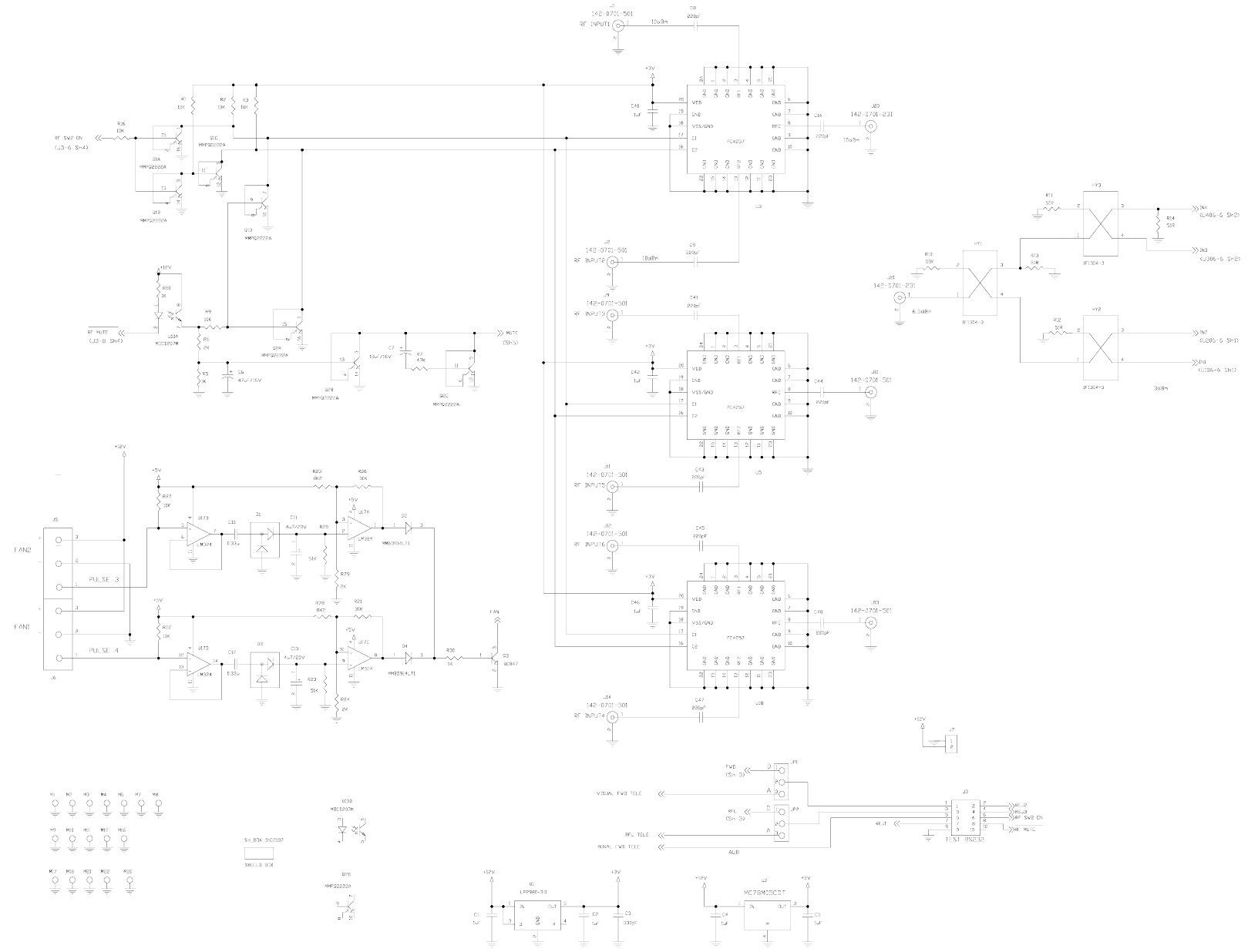
The signal from the Modulator 1 is applied to RF Input 1 and signal from the Modulator 2 is applied to RF Input 2 if
second Modulator is used. These signals are applied to RF switch U3. When there is no signal applied to
TELEMETRY pin 8 “SELECT MODULATOR 2” RF Input 1 is connected to 4-Way RF splitter HY1,HY2 and HY3 and
RF Input 2 is terminated to the internal U3 resistor 50 ohm. When the +12VDC signal is applied to the
TELEMETRY-8 “SELECT MODULATOR 2” RF Input 2 is connected to 4-Way RF splitter and RF Input 1 is
terminated. Signal from U3 switch is applied to connector J20 and trough coaxial cable to 4-Way RF Splitter input
connector J21. Signal from J21 is split 2,3 or 4 ways depending of the application. Depending of the number of the
channels used splitter outputs are applied to amplifiers or are terminated if amplifier is not used for specific group
assembly.
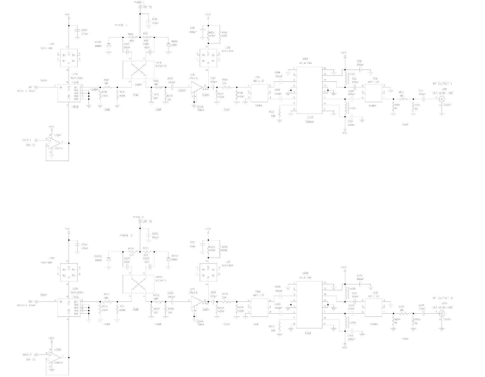
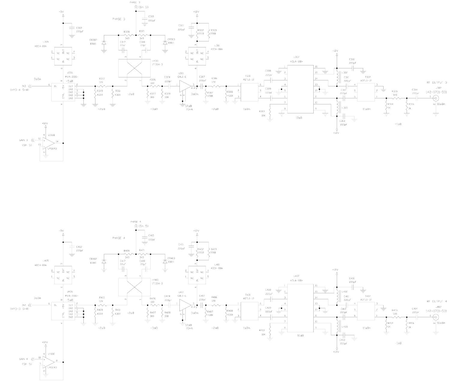
First stage in the amplifier chain is PIN attenuator U106 MVA-2000+ which gain is controlled by potentiometer
R104. Phase shifter built around 3dB coupler HY101 1F1304-3 provides necessary phase shift matching transmitter
cube combiner requirements. Phase adjustment can be done by front panel potentiometer R129. Following phase
shifter is RF amplifier U101 12dB gain and 2 dB pi attenuater R106/R107/R108.
Front panel phase adjustments allow fine-tuning of the match between the cube amplifiers by setting the overall
phase of each amplifier. These adjustments are frequency sensitive so there is no need to perform them in field.
U102 provides 11dB gain and requires significant cooling.
41D2355 4-WAY SPLITTER UHF
PUB13-01 Rev 0 Mar 4, 2013 13
7 SPECIFICATION
AC Input Voltage ................................................................................................... 90-264VAC line-to-neutral
AC Input Frequency .......................................................................................................................... 47-63Hz
AC Input Power ...................................................................................................................................... 40VA
Width - standard EIA rack size...................................................................................................................19"
Height ........................................................................................................................................ 2RU (3 1/2")
Depth ......................................................................................................................................................13"
Weight ..................................................................................................................................................10 lbs.
Cooling ........................................................................ 20 CFM, two 12VDC fans attached to the side panel
Humidity................................................................................................................................................to 90%
Altitude ..............................................................................................................................to 7500 ft (2286 m)
Fan FAULT indication .......................................................................................... provided on the front panel
AC ON indication.................................................................................................. provided on the front panel
Frequency range ........................................................................................................................ 470-860MHz
Nominal Output Impedance .................................................................................................................50ohm
Nominal input impedance all RF inputs ............................................................................................... 50ohm
Nominal input level RF INPUT 1 and 2 .......................................................................... +7dBm +/-2dB RMS
Nominal input level FWD (100% FWD)........................................................................ +20dBm +/-2dB RMS
Nominal input level RFL (10% RFL) ............................................................................. +10dBm +/-2dB RMS
Nominal input level REJ1,2,3 (100% REJ) .................................................................. +17dBm +/-2dB RMS
Overall gain ....................................................................................................................................... min 0dB
Phase adjustment range ............................................................................................................... min 50 deg
Gain adjustment range ..................................................................................................................... min -5dB
Output Return Loss ........................................................................................................................ min -10dB
Maximum output power ....................................................................................................................... 12dBm
Shoulders referenced to the haystack for ATSC standard ................................................................... -39dB
........................................................ (RBW 30kHz,VBW 30kHz,averaging 50,delta marker +/-3.2MHz)
41D2355 4-WAY SPLITTER UHF
PUB13-01 Rev 0 Mar 4, 2013 1
8 AMPLIFIERS TEST
1. Disconnect Power Supply from 4-Way Splitter PCB. Plug AC power cord. Check for 12VDC. Plug
J7 into PCB. Check front panel LED that indicates 12VDC from power supply. Check front panel
LED that indicates FAN operation.
2. Set the network analyzer frequency range from 470MHz to 860MHz.
Terminate the outputs of the Splitter.
Set network analyzer output power to 0 dBm.
Calibrate the analyzer for transmission measurement from J1 input to J102 output.
Set GAIN potentiometers for maximum gain for all 4 channels.
Check RF Switch function. Check the RF level at J2 input referenced to J1 input. It shall be
lower at least 55dB. Apply +5VDC to the J3-6/TELEMETRY-8. Check that channel #1 output
was reduced at least 55dB. Move the signal source to J2 input. Check Channel #1 output.
Remove +5VDC from J3-6/TELEMETRY-8. Check that channel #1 output was reduced at least
55dB. Move the signal source back to the J1 input.
Check GAIN adjustment range. It shall be at least 5dB. Adjust all channels gain to be 1dB less
than lowest maximum gain of all channels.
Check RF MUTE function by shorting J3-8/TELEMETRY-9 to GND. The output levels shall be
reduced by at least 25dB.
3. Set the network analyzer center frequency to 600MHz and SPAN to 5 MHz. Set frequency marker
to 600MHz.
Terminate the outputs of the Splitter.
Set network analyzer output power to 0 dBm.
Calibrate the analyzer for transmission measurement including channel 1.
Check phase adjustment range for channel 1. It shall be minimum 50 deg. Set channel 1 phase
in the middle of the adjustment range.
Calibrate again the analyzer for transmission measurement including channel 1.
Check adjustment range and adjust phase for all other channels referenced to channel 1
according to Table 1.

41D2355 4-WAY SPLITTER UHF
PUB13-01 Rev 0 Mar 4, 2013 2
AMP 1 2 3 4
Min phase [deg] -25 -115 -115 -225
Max phase [deg] +25 -65 -65 -155
Set phase [deg] 0 -90 -90 -180
Table 1
4. Check shoulders referenced to the haystack for standard M channels 14,40 and 69 at output
power 12dBm. Shoulders shall be better than 39dB – see specifications.
5. Simulate the failure of the FAN 1 by unplugging connector J5 . The LED FAN on the front panel
shall light up. Plug in connector J5. Repeat the test for FAN 2 by unplugging connector J6.
41D2355 4-WAY SPLITTER UHF
PUB13-01 Rev 0 Mar 4, 2013
Figure 1 4 Way Splitter Front and Rear View
41D2355 4-WAY SPLITTER UHF
PUB13-01 Rev 0 Mar 4, 2013
Figure 2 4-Way Splitter RF Flow Diagram 21B2917S1 sht1 Rev 0
41D2355 4-WAY SPLITTER UHF
PUB13-01 Rev 0 Mar 4, 2013
218002
Figure 3 4-Way Splitter UHF Schematic 41D2355S1 rev 0
41D2355 4-WAY SPLITTER UHF
PUB13-01 Rev 0 Mar 4, 2013
Figure 4 4-Way Splitter Assembly
41D2355 4-WAY SPLITTER UHF
PUB13-01 Rev 0 Mar 4, 2013
Figure 5 4-Way Splitter PCB Schematic 31C2007S1 sht 1 rev 0
41D2355 4-WAY SPLITTER UHF
PUB13-01 Rev 0 Mar 4, 2013
Figure 6 4-Way Splitter PCB Schematic 31C2007S1 sht 2 rev 0
41D2355 4-WAY SPLITTER UHF
PUB13-01 Rev 0 Mar 4, 2013
Figure 7 4-Way Splitter PCB Schematic 31C2007S1 sht 3 rev 0
41D2355 4-WAY SPLITTER UHF
PUB13-01 Rev 0 Mar 4, 2013
Figure 8 4-Way Splitter PCB Schematic 31C2007S1 sht 4 rev 0
41D2355 4-WAY SPLITTER UHF
PUB13-01 Rev 0 Mar 4, 2013
Figure 9 4-Way Splitter PCB Schematic 31C2007S1 sht 5 rev 0
41D2355 4-WAY SPLITTER UHF
PUB13-01 Rev 0 Mar 4, 2013
Figure 10 4-Way Splitter PCB Schematic 31C2007S1 sht 6 rev 0
41D2355 4-WAY SPLITTER UHF
PUB13-01 Rev 0 Mar 4, 2013
Figure 11 4-Way Splitter PCB Assembly 31C2007A1 sht 1 rev 0