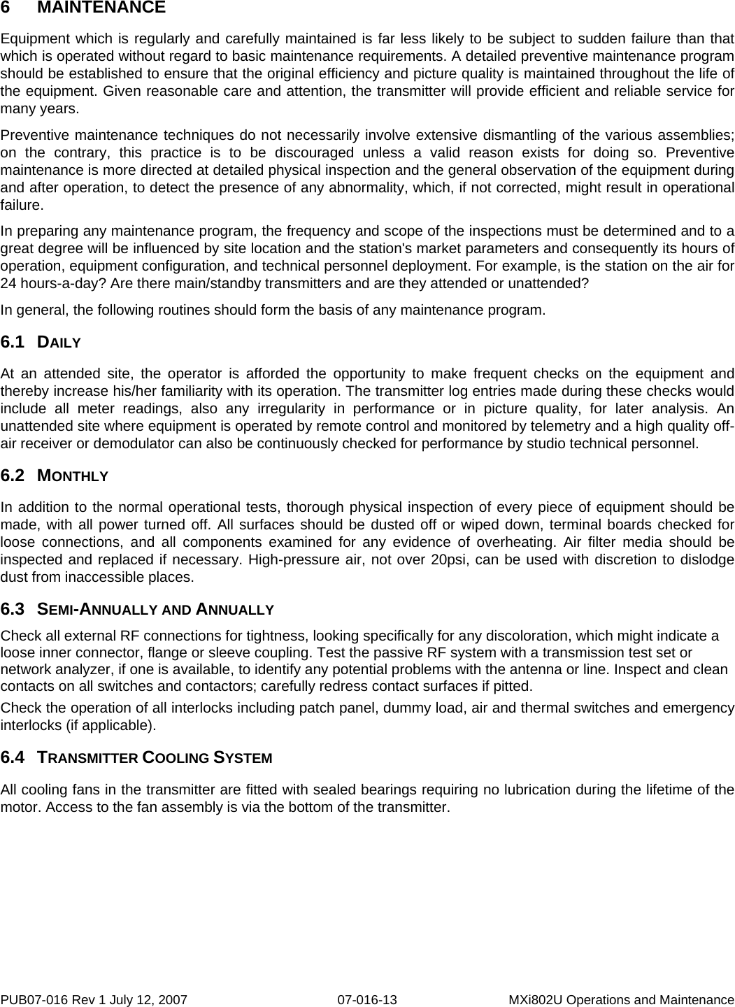
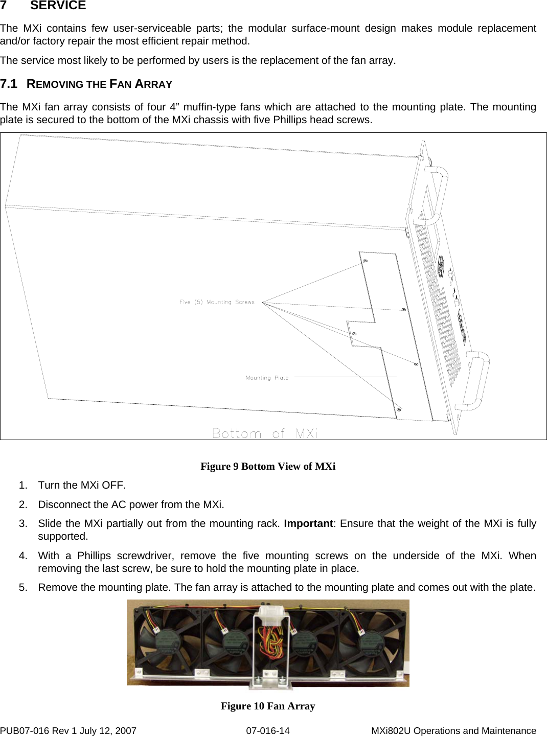
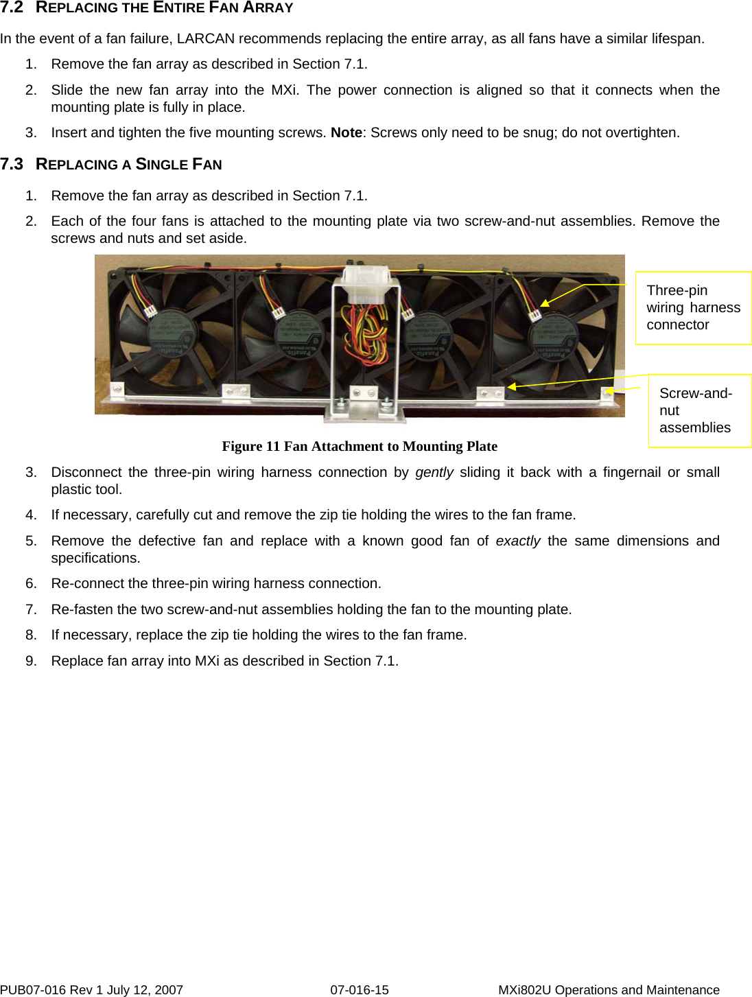
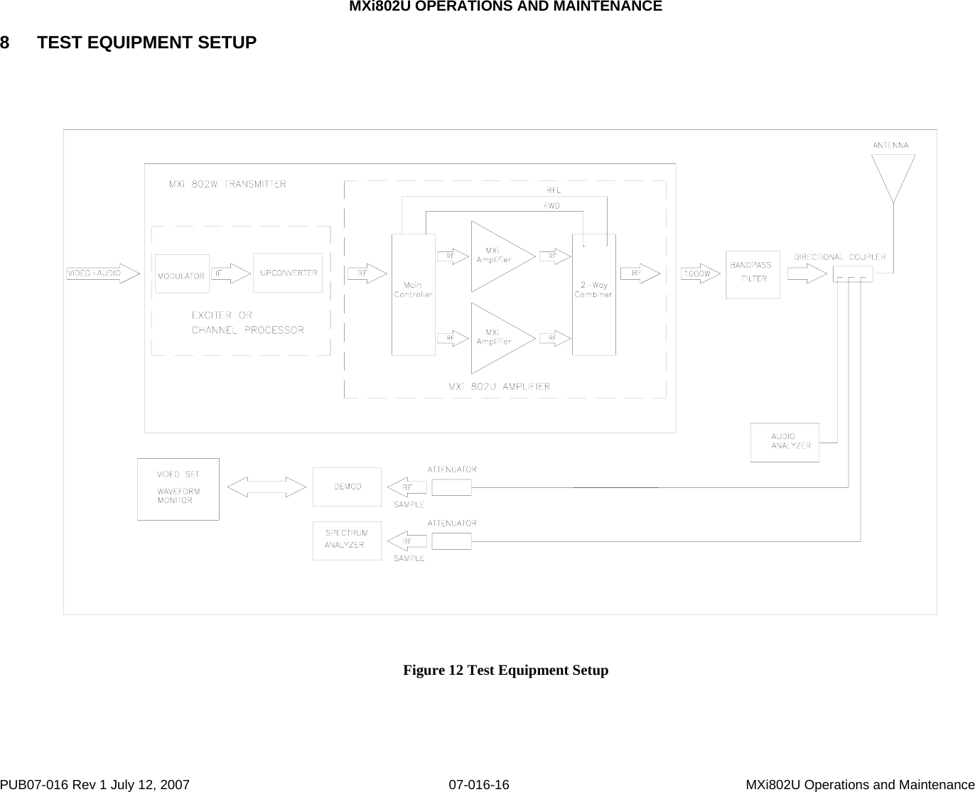
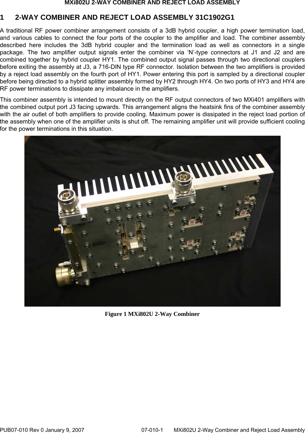
Larcan MXI802U Digital Broadcast Translator User Manual
Larcan Inc Digital Broadcast Translator
UserManual.wiki
>
Larcan
>
MXI802U User Manual
user manual
Navigation menu
Upload a User Manual
Namespaces
Wiki Guide
HTML
PDF
Info
Views
User Manual
Discussion / Help
Navigation
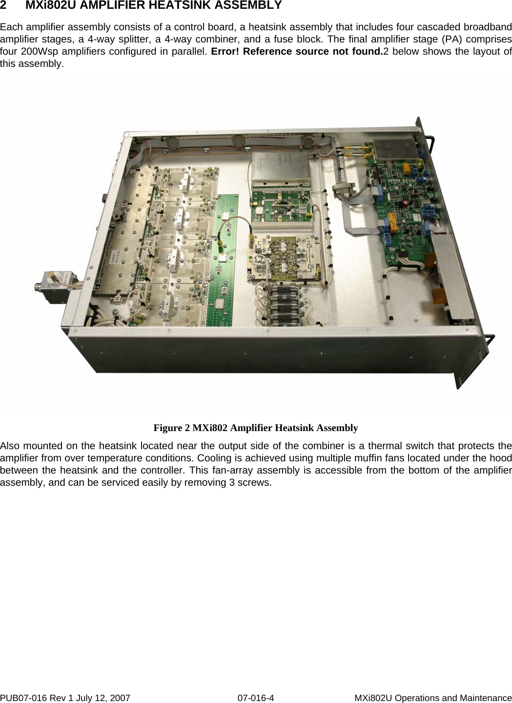

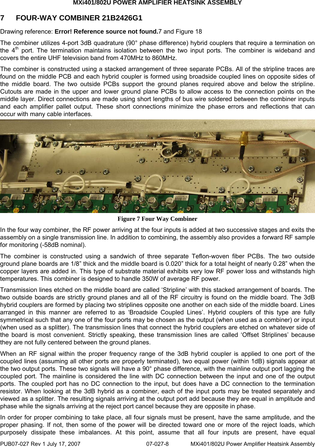
![MXi401/802U POWER AMPLIFIER HEATSINK ASSEMBLY PUB07-027 Rev 1 July 17, 2007 07-027-9 MXi401/802U Power Amplifier Heatsink Assembly amplitudes and the proper phasing. Power at combiner input ports J1 and J2 is combined at the output of HY1 and becomes one of the input signals to HY3. The same occurs with the power entering at ports J3 and J4 – it adds at the output port of HY2 which in turn is connected to the other input port of HY3. The combined power appearing at the output of HY3 is then directed through a directional coupler before reaching the combined output port at J5. The power handling capacity of the combiner is limited by the power rating of the balancing terminations used. These balancing terminations, or reject loads, are used to absorb power that would otherwise be reflected or directed toward other amplifier outputs. If an amplifier pallet output power is reduced, or drops to zero (in the case of DC power removal due to a blown fuse), some power from the remaining amplifiers will be dissipated in the reject loads. As an example, if the DC power were removed from the amplifier pallet on input J1, then half of the power at input J2 is directed into reject load R1. This occurs because 3dB hybrid coupler HY1 has only a single input and now acts as a splitter. As a result of the reduced power at the output of HY1, some power will also be dissipated in R3. The worst case scenario involves the complete shutdown of a pair of amplifiers with zero power entering either ports J1 and J2 or ports J3 and J4. The combined power of two of the pallets is applied to one port of HY3 and no power appears at the second input of HY3. HY3 now acts as a power splitter and directs half of the power toward the reject termination. As an example, if the RF power from each pallet is 100W, then the power applied to one input of HY3 would be 200W which would then be divided between the output and reject ports of HY3. Under these conditions, the reject load would be required to dissipate 100W. The terminations used on the combiner have an individual power rating of 250W average RF power, but we typically de-rate them by at least half in order to ensure long term reliability. The formulas following this paragraph may be used to determine the level of reject power in any particular reject load based on the input power to that hybrid coupler. For a single 3dB hybrid coupler: Pout = ½(P1 + P2) + [√(P1P2)]cosθ Prej = ½(P1 + P2) – [√(P1P2)]cosθ P1 and P2: power at each input port Pout: combined output power Prej: power dissipated in the reject load Θ: phase error between P1 and P2 (Θ=0 assumed) Total Output and Reject Power PTout = [1-(n/4)]² x 100% in a Four Way Combiner: PTrej = 1/4[n-(n²/4)] x 100% PTout: total combined power at the combiner output port as a percentage of the rated output power PTrej: total power dissipated in reject loads expressed as a percentage of the rated output power n: number of pallet amplifiers not supplying power to the combiner Example: If one pallet amplifier is not supplying power, then n=1 and the power appearing at the combined output and in the reject loads is as follows: PTout = [1-(1/4)]² x 100% = 56% (of rated output) PTrej = 1/4[(1-(n²/4)] x 100% = 19% (of rated output)](https://usermanual.wiki/Larcan/MXI802U/User-Guide-1187355-Page-30.png)
![MXi401/802U POWER AMPLIFIER HEATSINK ASSEMBLY PUB07-027 Rev 1 July 17, 2007 07-027-10 MXi401/802U Power Amplifier Heatsink Assembly It should be noted that the total power (56+19=75%) represents the input power as a percentage of the rated output power [1-(n/4)] x 100%. The value of PTrej is the total power dissipated in all of the reject loads. In order to calculate the power in a particular load, then the formula for a single 3dB hybrid coupler must be used. As an example, assume a total combined output of 300W average RF power from the combiner and 75W at each input (disregarding losses). Using the same example as above, assume that no power enters at J1. The resulting power dissipated in R1and R3 is calculated as follows (assume ideal phasing in all cases cosθ=1): Refer to schematic drawing 21B2426S1 as a guide HY1: power into J2 = 75W (P1=75) power into J1 = 0W (P2=0) Pout = ½(P1 + P2) + [√(P1P2)]cosθ = ½(75 + 0) + [[√(75x0)]cosθ = 37.5W Prej = ½(P1 + P2) – [√(P1P2)]cosθ = ½(75 + 0) – [√(75x0)]cosθ = 37.5W Power into J1+J2 input of HY3 = 37.5W Power into R1 = Prej = 37.5W HY2: power into J3 = 75W (P1=75) power into J4 = 75W (P2=75) Pout = ½(P1 + P2) + [√(P1P2)]cosθ = ½(75 + 75) + [[√(75x75)]cosθ = 150W Prej = ½(P1 + P2) – [√(P1P2)]cosθ = ½(75 + 75) – [√(75x75)]cosθ = 0W Power into J3+J4 input of HY3 = 150W Power into R2 = Prej = 0W HY3: power into J1+J2 input = 37.5W (P1=37.5) power into J3+J4 input = 150W (P2=150W) Pout = ½(P1 + P2) + [√(P1P2)]cosθ = ½(37.5 + 150) + [[√(37.5x150)]cosθ = 168.8W Prej = ½(P1 + P2) – [√(P1P2)]cosθ = ½(37.5 + 150) – [√(37.5x150)]cosθ = 18.8W](https://usermanual.wiki/Larcan/MXI802U/User-Guide-1187355-Page-31.png)
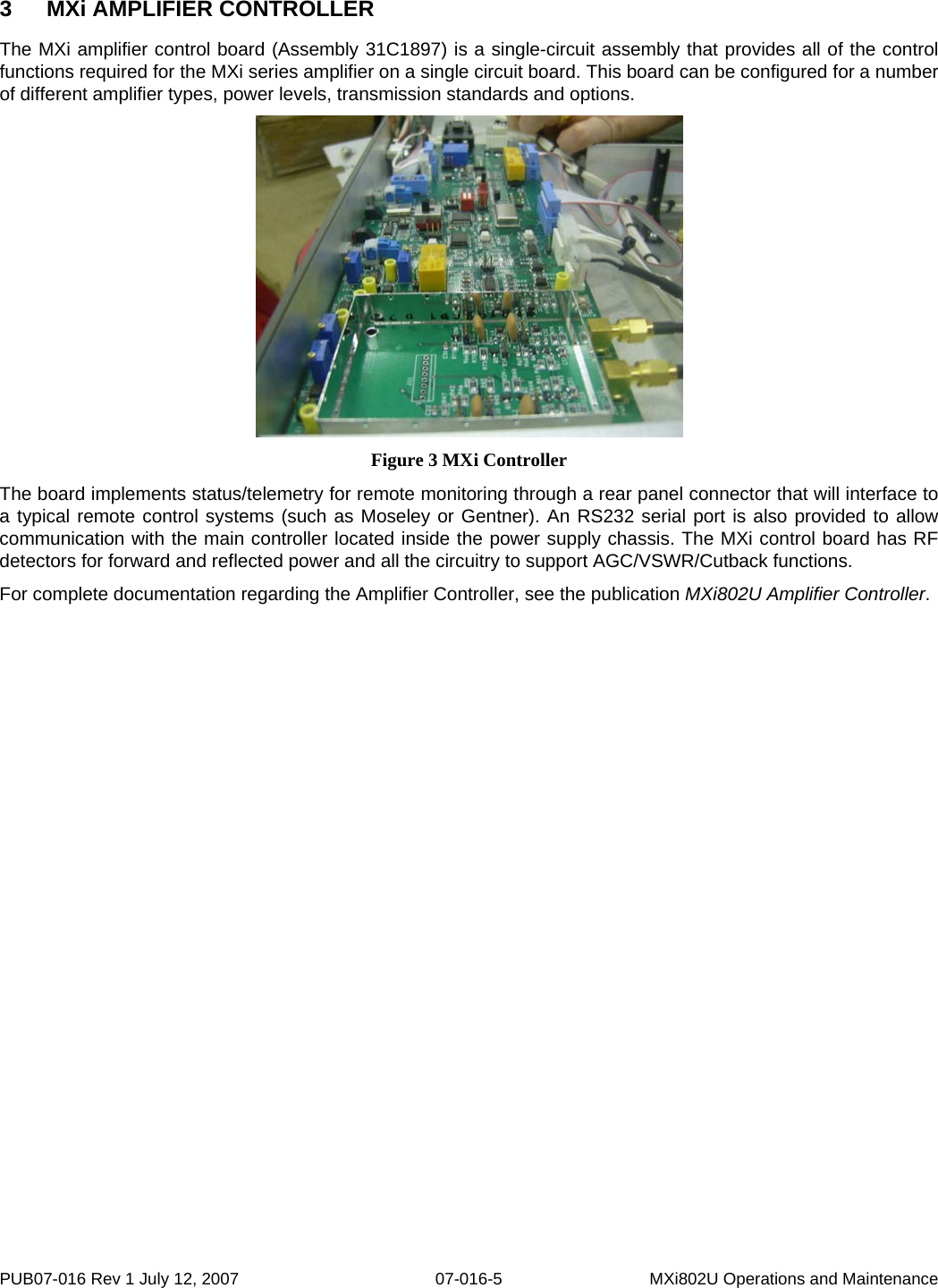
![MXi802U 2-WAY COMBINER AND REJECT LOAD ASSEMBLY PUB07-010 Rev 0 January 9, 2007 07-010-2 MXi802U 2-Way Combiner and Reject Load Assembly 2 CIRCUIT DESCRIPTION: COMBINER ASSEMBLY RF power from the two MXi401 amplifier assemblies enters the combiner at J1 and J2. In order for proper combining to take place, these two signals must be the same amplitude and in quadrature phase (ie. 90° phase difference with J1 lagging J2). The proper phasing is provided by the RF splitter that feeds the two amplifiers. A similar wide band quadrature hybrid is used to split the RF signal, but each signal also passes through a variable phase circuit to correct for any errors in the cables feeding the amplifiers. The hybrid couplers described here are constructed from coupled transmission lines, essentially two lines etched on either side of a printed circuit board (PCB) directly over top of one another. Transmission lines arranged in this manner are referred to as ‘Broadside Coupled Lines’. These coupled lines (and all interconnecting lines) are etched on a ceramic-loaded Teflon-fiber substrate that is 0.020” thick and referred to as the middle board or coupled section. On either side of this middle board is a 1/8” thick board of the same material with full ground plane on the outside surface. The entire sandwich is nearly 0.28” thick when all of the copper layers are added in. A lot of heat is generated by the insertion loss of the 3dB coupler when it is used at such high power. The ceramic-loaded Teflon-fiber PCB substrate has a rather high thermal conductivity rating and so it is able to transfer the heat to the heatsink on which the boards are mounted. Hybrid couplers of this type are fully symmetrical such that any one of the four ports may be chosen as the output (when used as a combiner) or input (when used as a splitter). The transmission lines that connect the hybrid couplers to the input and output ports are etched on whatever side of the middle board is most convenient. Strictly speaking, these transmission lines are called ‘Offset Striplines’ because they are not fully centered between the ground planes. When an RF signal within the proper frequency range of the 3dB hybrid coupler is applied to one port of the coupled lines (assuming all other ports are properly terminated), two signals of equal power (within 1dB) appear at the two output ports. These two signals will have a 90° phase difference, with the mainline output port lagging the coupled port. The mainline is considered the line with DC connection between the input and one of the output ports. The coupled port has no DC connection to the input, but does have a DC connection to the termination resistor. When looking at the 3dB hybrid as a combiner, each of the input ports may be treated separately and viewed as a splitter. The resulting signals arriving at the output port add since they are equal in amplitude and phase while the signals arriving at the reject port cancel because they are opposite in phase. The following formulas may be used to determine the power level at both the combined output and reject ports of the coupler For a single 3dB hybrid coupler: Pout = ½(P1 + P2) + [√(P1P2)] cosθ {1} Prej = ½(P1 + P2) – [√(P1P2)] cosθ {2} P1 and P2: power at each input port Pout: combined output power Prej: power dissipated in the reject load Θ: phase error between P1 and P2 Maximum combined output power is achieved when power directed to the reject load is at a minimum. This occurs when the two input signals have the same amplitude (P1=P2) and the phase error between the two signals is zero (Θ=0°). Whenever there is a phase error and/or an amplitude difference, then some of the available power is directed to the reject load. The maximum power level in the reject load occurs when only a single amplifier is operating into the combiner HY1. The hybrid then acts as a signal splitter, sending half of the input power to combined output and the other half to the reject load. Referring to formulas {1} and {2}, when either P1=0 or P2=0, the second term in each expression reduces to zero and the result is Pout=Prej=½P1 or ½P2, depending on which one is off. When power is directed to the reject port of the hybrid HY1, it is dissipated in power terminations R17 through R20.](https://usermanual.wiki/Larcan/MXI802U/User-Guide-1187355-Page-44.png)
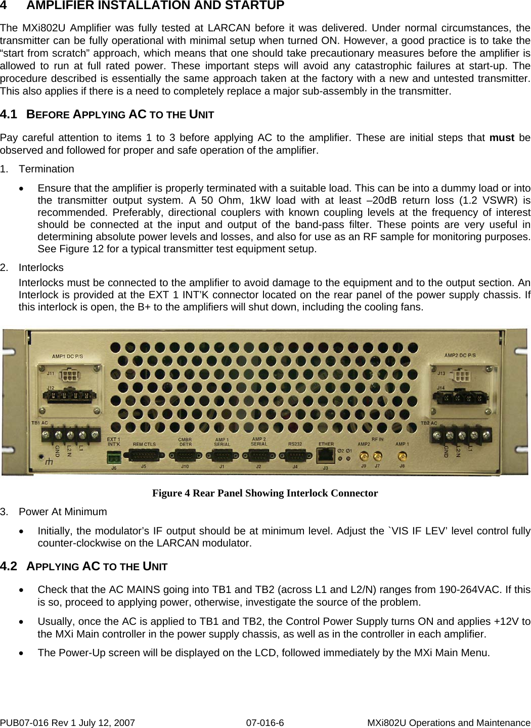
![MXi802U AMPLIFIER CONTROLLER BOARD REV.2 PUB07-012 Rev 0 January 10, 2006 07-012-8 MXi802U Amplifier Controller Board Rev.2 Note the AGC voltage from the LCD, if it is near to a value of 0 (i.e., under 0.1V), then there is no AGC action left and the power cannot be raised any further. If the amplifier power is under 100%, then check the RFL power level and CUTBACK voltage to verify that the amplifier is not reducing power to protect from a VSWR condition. The cutback circuit checks the level of reflected power as displayed on the LCD screen above [RFL=00.1%]. If this reflected power is greater than 1%, the cutback circuit automatically reduces the amplifier forward power to protect the devices. This indicates a mild VSWR condition such as may be caused by an icy antenna. The cutback function is a safety protection and is therefore permanently in circuit and cannot (or should not) be disabled. If the VSWR condition worsens such that reflected power exceeds 10% of forward power, the MXi shuts the transmitter down. The MXi has built-in VSWR protection to prevent damage to the amplifier from excessive power being reflected back from the output system. This VSWR protection becomes operational when reflected power exceeds 10% of forward power. The system shuts down the amplifier for a few seconds and then tries to restart again. This is done to check if the VSWR was a temporary condition that could have been caused by a lightning strike nearby. The LCD shows the TRIP status light on the third row of the LCD to indicate that a VSWR trip had occurred. If the condition persists such that three VSWR trips occur within 1 minute, the system completely shuts down. The LCD will then illuminate the L/O (Lockout) status light on the LCD to show that a Lockout has occurred. 2.5 INTERLOCKS Interlocks on the MXi amplifier can be divided into two different types: hard interlocks that shut down the amplifier without any CPU intervention and soft interlocks that are generated by the CPU chip in response to abnormal system parameters. 2.5.1 Hard Interlocks There are hardware interlocks that directly affect the ON/OFF relay K1 by removing the +12V arming voltage on its coil and preventing it from turning on. There are four of these interlocks as follows: 2.5.1.1. Amplifier Thermal Heatsink thermal opens if heatsink temperature is too high. Dry Contact across Connector J9 pins 5 and 6. 2.5.1.2. Transmitter Switching Interlock provided for an external Transmitter Switching unit to shut down the Transmitter. Dry Contact across Connector J7 pins 1 and 2. When there is no transmitter switching, jumper E6 defeats this interlock. 2.5.1.3. External #1 Interlock supplied for customer use such as RF system interlock or RF Load. Dry Contact across Connector J9 pins 1 and 2. Parallel contact provided across J6 pins 14 and 15, only one of J6 or J9 is required. If not used, then this contact should be shorted out externally. 2.5.1.4. VSWR Relay K2 Contact from VSWR Trip relay K2 pins 11 and 13. Contact will be closed (OK) if there is no VSWR condition. Contact will open whenever a VSWR is detected. Note: Jumper E17 disables this interlock, this is for setup only.](https://usermanual.wiki/Larcan/MXI802U/User-Guide-1187355-Page-57.png)
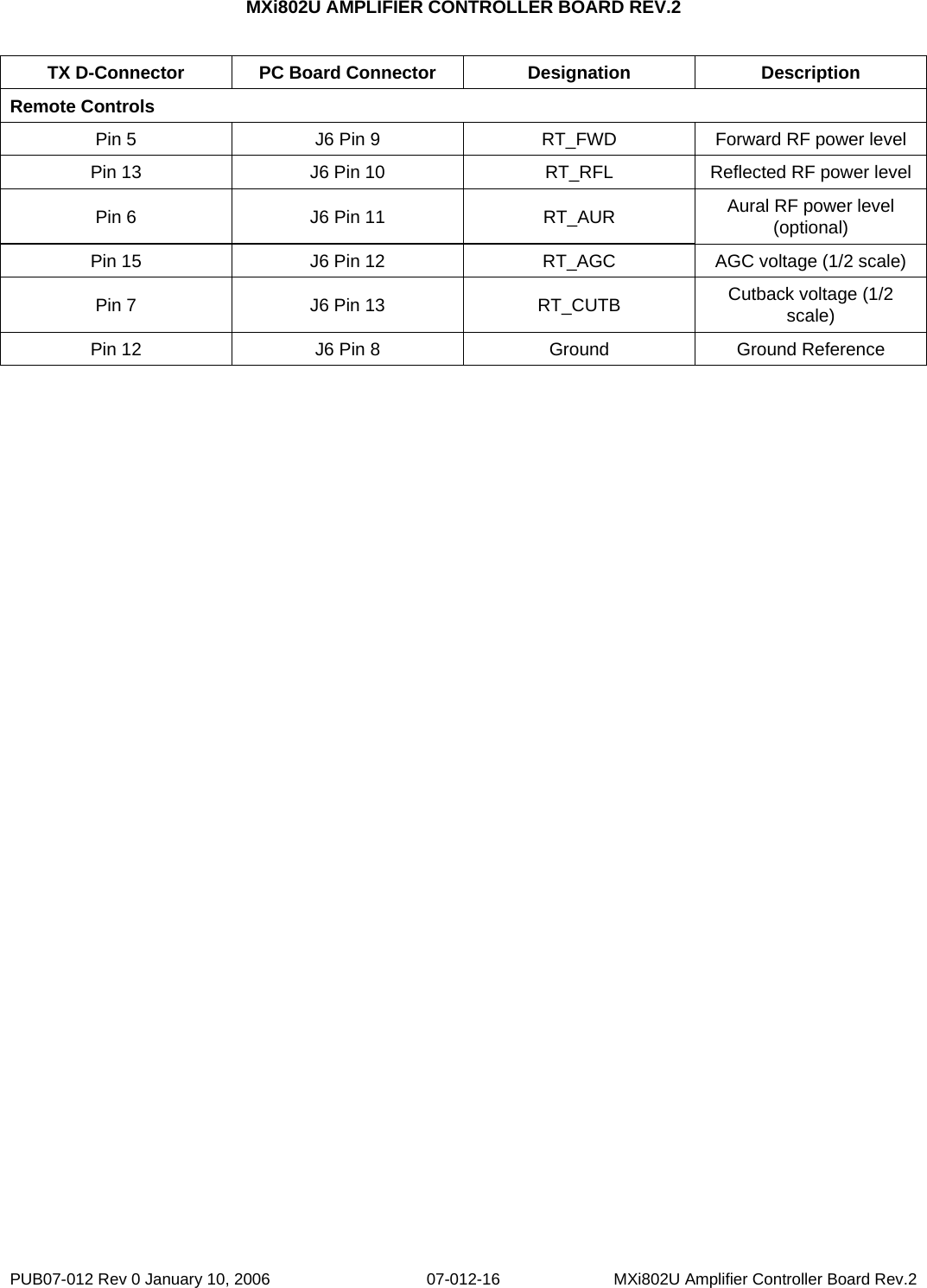
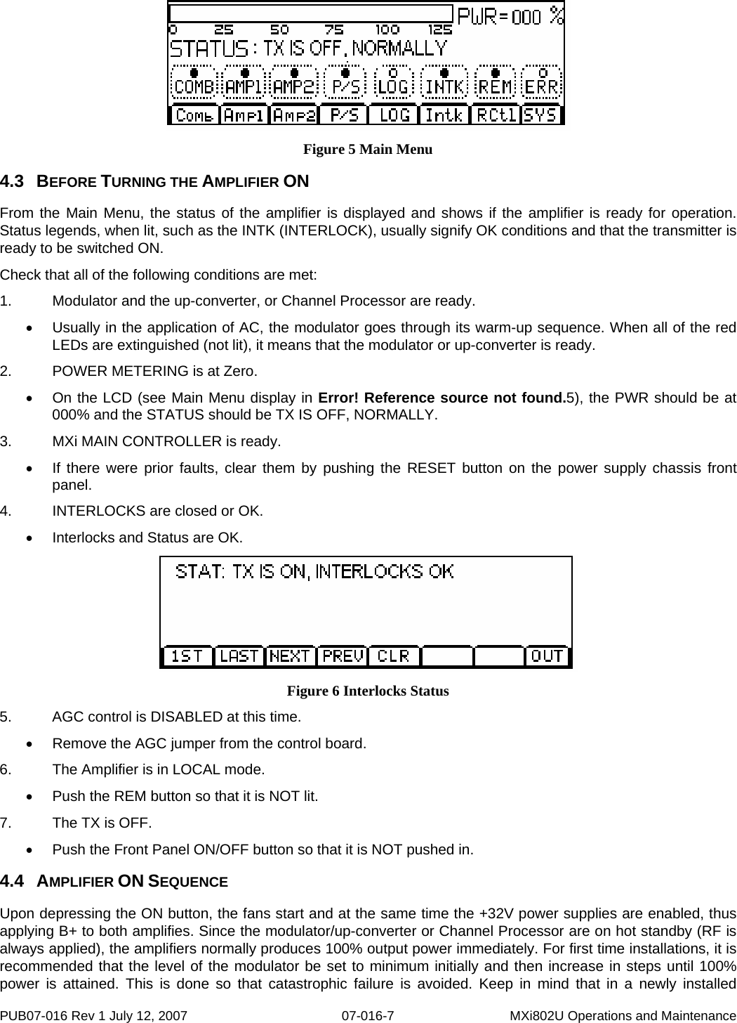
![MXi802U AMPLIFIER CONTROLLER BOARD REV.2 PUB07-012 Rev 0 January 10, 2006 07-012-17 MXi802U Amplifier Controller Board Rev.2 5 CIRCUIT DESCRIPTIONS 5.1 MC68HC908 MICROPROCESSOR The Motorola MC68HC908GT microprocessor (often referred to as the CPU or HC08) performs all of the control interface and communications in the MXi transmitter system. It is a 44-pin surface mount PLCC type device that is permanently soldered to the circuit board and is not field serviceable or easily replaced without special surface mount tooling. A brief description of the part is given in this section and a portion of the manufacturer’s documentation is given in Appendix A. More detailed information on this part can be obtained from the Motorola web site. The HC08 chip used in the MXi can come with either 8K or 16K bytes of non-volatile flash memory, which can be erased and reprogrammed to allow updating of software code or system parameters. The MXi code is typically smaller than 8k and so would fit in either size of Flash memory. The HC08 chip has a dedicated serial input pin designated as the BDM (Background Debug Mode) port that is used to program the internal Flash memory and for debug testing. The MXi is programmed at the factory and it is not expected that reprogramming would need be done in the field, although it is possible to do with the proper software. System parameters and status that need to be retained during power failures (such as the LOG entries) are also stored in the Flash memory. Most of the external pins on the HC08 are configured as programmable Input/Output (I/O) ports, where the software program determines whether a certain pin is to be configured as either an input or output. The pins on the HC08 are grouped together in sets called PORTs. These Ports will have eight pins (or fewer) to support the byte wide data path in the CPU. Port A is used for general system inputs and outputs. Port B is used as an eight-channel A/D converter to measure system telemetry values. Port C is used for general system inputs and outputs. Port D assigns four pins for the synchronous serial port (SPI) with the other four pins used for system inputs. Port E assigns two pins as a serial communications port (SCI), one pin is the external CPU clock and the other two pins used for general system inputs and outputs. The definition of each Port pin is as follows: PORT A PA0 Input or Output Jumper E3 configures as I/P or O/P PA1 Input Remote Control ON Command PA2 Input Remote Control OFF Command PA3 Output Select enable for Serial NvPot U16 PA4 Input Front Panel ON Command PA5 Input Front Panel VSWR RESET Command PA6 Input 32V Power Supply OK Status PA7 Input Remote Control VOR Status PORT B PB0 Telemetry Temperature of Heatsink [Optional] PB1 Telemetry Power Supply Current PB2 Telemetry Power Supply Volts PB3 Telemetry Cutback Volts [Scaled at half the actual value] PB4 Telemetry AGC Volts [Scaled at half the actual value] PB5 Telemetry RF Aural Power [from RF detector - Optional] PB6 Telemetry RF Reflected Power [from RF detector] PB7 Telemetry RF Forward Power [from RF detector]](https://usermanual.wiki/Larcan/MXI802U/User-Guide-1187355-Page-66.png)
![MXi802U AMPLIFIER CONTROLLER BOARD REV.2 PUB07-012 Rev 0 January 10, 2006 07-012-18 MXi802U Amplifier Controller Board Rev.2 PORT C PC0 Output Remote Status – Error PC1 Input DipSw #1 PC2 Input Power Supply (Relay K1) ON Status PC3 Input DipSw #2 PC4 Input External #1 Interlock PC5 Output VSWR Reset Control PC6 Output PS ON Ctl +12V out [could be 24V too] PORT D PD0 SPI SS Used by UART PD1 SPI MISO Used by UART and NvPot PD2 SPI MOSI Used by UART and NvPot PD3 SPI SCLK Used by UART and NvPot PD4 Input Fan#1 Status, Active Low PD5 Input Fan#2 Status, Active Low PD6 Input Fan#3 Status, Active Low PD7 Input Fan#4 Status, Active Low PORT E PE0 SCI Transmit Data Used by LCD PE1 SCI Receive Data Used by LCD PE2 O/P Remote Status – Remote Mode PE3 Input VSWR Trip Status PE4 System Main CPU Clock – 4.9152MHz The HC08 provides two separate serial interfaces to external components, these are the synchronous peripheral interface (SPI) and the serial communications interface (SCI). The SCI implements the standard three-wire serial port (Rx Data, Tx Data and Ground) that would interface to a typical computer port. The baud is set at 9600. The baud is derived from the system oscillator clock at 4.9152MHz. This frequency is recommended by the manufacturer to easily obtain the most common bauds. The SPI implements a four-wire clocked serial port that has four signals, Slave Select (SS), Master Out Slave In (MOSI), Master In Slave Out (MISO) and Serial Clock (SCLK). The HC08 is always set as the Master who initiates all serial communications. The SPI port is used to communicate with the MAX3110 UART (U2) and the DS1867 NovPot (U16). The HC08 will send out it data stream from the MOSI line and reads any responses from the external (Slave) devices via the MISO line. The SCLK is a serial clock (set for around 64K baud) that synchronizes the data transfer. The presence of this clock allows must higher data rates than the asynchronous SCI serial protocol. The SS line is a select that enables the MAX 3110 UART when low. A second individual select line from Port A (pin PA3) is used to select the DS1867 NovPot. 5.2 POWER SUPPLY VOLTAGE AND CURRENT MONITORING For the following description, refer to Figure 6 (Sheet #2 of the Schematic) in the upper section of the drawing for the power supply monitoring circuitry. The first section describing the on-board current sensor is for reference only since it is not used for the Mxi802 type transmitters.](https://usermanual.wiki/Larcan/MXI802U/User-Guide-1187355-Page-67.png)