Larcan MXI802U Digital Broadcast Translator User Manual
Larcan Inc Digital Broadcast Translator
Larcan >
user manual
PUB07-016 Rev 1 July 12, 2007 07-016-1 MXi802U Operations and Maintenance
CONTENTS
1 THE MXi802 TRANSMITTER........................................................................................................................................3
2 MXi802U AMPLIFIER HEATSINK ASSEMBLY........................................................................................................4
3 MXi AMPLIFIER CONTROLLER.................................................................................................................................5
4 AMPLIFIER INSTALLATION AND STARTUP..........................................................................................................6
4.1 BEFORE APPLYING AC TO THE UNIT ............................................................................................................................6
4.2 APPLYING AC TO THE UNIT..........................................................................................................................................6
4.3 BEFORE TURNING THE AMPLIFIER ON .........................................................................................................................7
4.4 AMPLIFIER ON SEQUENCE............................................................................................................................................7
4.4.1 Turning ON the MXi Transmitter.........................................................................................................................8
4.4.2 TYPICAL DATA read on the LCD .......................................................................................................................9
5 TEST AND TROUBLESHOOTING .............................................................................................................................10
5.1 BENCH TEST PROCEDURES .........................................................................................................................................10
5.1.1 Front-End Module, 21B1473, Bench Test Procedure........................................................................................10
5.1.2 IPA1, 21B1324, Bench Test Procedure..............................................................................................................10
5.1.3 Driver Pallet, 21B1639, Bench Test Procedure.................................................................................................11
5.1.4 PA Pallet 11A2142G1 Bench Test Procedure....................................................................................................11
5.2 BASIC TROUBLESHOOTING TECHNIQUES ....................................................................................................................12
5.2.1 No RF Output.....................................................................................................................................................12
5.2.2 Output Reduced to 25% .....................................................................................................................................12
6 MAINTENANCE.............................................................................................................................................................13
6.1 DAILY.........................................................................................................................................................................13
6.2 MONTHLY...................................................................................................................................................................13
6.3 SEMI-ANNUALLY AND ANNUALLY .............................................................................................................................13
6.4 TRANSMITTER COOLING SYSTEM ...............................................................................................................................13
7 SERVICE..........................................................................................................................................................................14
7.1 REMOVING THE FAN ARRAY.......................................................................................................................................14
7.2 REPLACING THE ENTIRE FAN ARRAY .........................................................................................................................15
7.3 REPLACING A SINGLE FAN..........................................................................................................................................15
8 TEST EQUIPMENT SETUP..........................................................................................................................................16
9 SPECIFICATIONS .........................................................................................................................................................17
9.1 ELECTRICAL ...............................................................................................................................................................17
9.2 ENVIRONMENTAL .......................................................................................................................................................17
9.3 COOLING ....................................................................................................................................................................17
9.4 DIMENSIONS ...............................................................................................................................................................17
9.5 SHIPPING WEIGHT ......................................................................................................................................................17
FIGURES
FIGURE 1 MXI802 POWER SUPPLY (TOP), AND AMPLIFIERS.........................................................................................................3
FIGURE 2 MXI802 AMPLIFIER HEATSINK ASSEMBLY...................................................................................................................4
FIGURE 3 MXI CONTROLLER........................................................................................................................................................5
FIGURE 4 REAR PANEL SHOWING INTERLOCK CONNECTOR .........................................................................................................6
FIGURE 5 MAIN MENU..................................................................................................................................................................7
FIGURE 6 INTERLOCKS STATUS ....................................................................................................................................................7
FIGURE 7 TRANSMITTER ON ........................................................................................................................................................8
FIGURE 8 AGC ADJUSTMENT .......................................................................................................................................................8
PUB07-016 Rev 1 July 12, 2007 07-016-2 MXi802U Operations and Maintenance
FIGURE 9 BOTTOM VIEW OF MXI...............................................................................................................................................14
FIGURE 10 FAN ARRAY ..............................................................................................................................................................14
FIGURE 11 FAN ATTACHMENT TO MOUNTING PLATE.................................................................................................................15
FIGURE 12 TEST EQUIPMENT SETUP ...........................................................................................................................................16
PUB07-016 Rev 1 July 12, 2007 07-016-3 MXi802U Operations and Maintenance
1 THE MXi802 TRANSMITTER
The MXi802 analog transmitter is usually comprised of a LARCAN IF Modulator, UHF Up-converter, a Power
supply chassis, and two Amplifier chassis. In some cases the modulator/up-converter combination is replaced by
a single unit Exciter or Channel Processor.
The RF section of the MXi802U consists of two identical amplifiers configured to operate in quadrature. Each
amplifier is capable of delivering power over 500 Watts sync peak. The output of these amplifiers are fed into a
two-way combiner assembly with built-in reject loads, and RF detectors which are used for protection and
metering purposes. Therefore, in this configuration, the MXi802 is capable of delivering RF power of up to 1kW
sync peak with exceptional performance and reliability.
The power supply chassis (top unit shown in Fig.1) contains the main controller board, LCD display, and two high
efficiency dual output (+12VDC and +32VDC) switching power supplies. The +12VDC power supply provides
power to the controllers, and the +32V supplies power to the amplifiers. Each power supply unit is rated at 2kW.
Figure 1 MXi802 Power Supply (top), and Amplifiers
PUB07-016 Rev 1 July 12, 2007 07-016-4 MXi802U Operations and Maintenance
2 MXi802U AMPLIFIER HEATSINK ASSEMBLY
Each amplifier assembly consists of a control board, a heatsink assembly that includes four cascaded broadband
amplifier stages, a 4-way splitter, a 4-way combiner, and a fuse block. The final amplifier stage (PA) comprises
four 200Wsp amplifiers configured in parallel. Error! Reference source not found.2 below shows the layout of
this assembly.
Figure 2 MXi802 Amplifier Heatsink Assembly
Also mounted on the heatsink located near the output side of the combiner is a thermal switch that protects the
amplifier from over temperature conditions. Cooling is achieved using multiple muffin fans located under the hood
between the heatsink and the controller. This fan-array assembly is accessible from the bottom of the amplifier
assembly, and can be serviced easily by removing 3 screws.
PUB07-016 Rev 1 July 12, 2007 07-016-5 MXi802U Operations and Maintenance
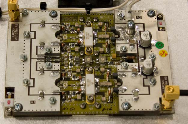
3 MXi AMPLIFIER CONTROLLER
The MXi amplifier control board (Assembly 31C1897) is a single-circuit assembly that provides all of the control
functions required for the MXi series amplifier on a single circuit board. This board can be configured for a number
of different amplifier types, power levels, transmission standards and options.
Figure 3 MXi Controller
The board implements status/telemetry for remote monitoring through a rear panel connector that will interface to
a typical remote control systems (such as Moseley or Gentner). An RS232 serial port is also provided to allow
communication with the main controller located inside the power supply chassis. The MXi control board has RF
detectors for forward and reflected power and all the circuitry to support AGC/VSWR/Cutback functions.
For complete documentation regarding the Amplifier Controller, see the publication MXi802U Amplifier Controller.
PUB07-016 Rev 1 July 12, 2007 07-016-6 MXi802U Operations and Maintenance
4 AMPLIFIER INSTALLATION AND STARTUP
The MXi802U Amplifier was fully tested at LARCAN before it was delivered. Under normal circumstances, the
transmitter can be fully operational with minimal setup when turned ON. However, a good practice is to take the
“start from scratch” approach, which means that one should take precautionary measures before the amplifier is
allowed to run at full rated power. These important steps will avoid any catastrophic failures at start-up. The
procedure described is essentially the same approach taken at the factory with a new and untested transmitter.
This also applies if there is a need to completely replace a major sub-assembly in the transmitter.
4.1 BEFORE APPLYING AC TO THE UNIT
Pay careful attention to items 1 to 3 before applying AC to the amplifier. These are initial steps that must be
observed and followed for proper and safe operation of the amplifier.
1. Termination
• Ensure that the amplifier is properly terminated with a suitable load. This can be into a dummy load or into
the transmitter output system. A 50 Ohm, 1kW load with at least –20dB return loss (1.2 VSWR) is
recommended. Preferably, directional couplers with known coupling levels at the frequency of interest
should be connected at the input and output of the band-pass filter. These points are very useful in
determining absolute power levels and losses, and also for use as an RF sample for monitoring purposes.
See Figure 12 for a typical transmitter test equipment setup.
2. Interlocks
Interlocks must be connected to the amplifier to avoid damage to the equipment and to the output section. An
Interlock is provided at the EXT 1 INT’K connector located on the rear panel of the power supply chassis. If
this interlock is open, the B+ to the amplifiers will shut down, including the cooling fans.
Figure 4 Rear Panel Showing Interlock Connector
3. Power At Minimum
• Initially, the modulator’s IF output should be at minimum level. Adjust the `VIS IF LEV’ level control fully
counter-clockwise on the LARCAN modulator.
4.2 APPLYING AC TO THE UNIT
• Check that the AC MAINS going into TB1 and TB2 (across L1 and L2/N) ranges from 190-264VAC. If this
is so, proceed to applying power, otherwise, investigate the source of the problem.
• Usually, once the AC is applied to TB1 and TB2, the Control Power Supply turns ON and applies +12V to
the MXi Main controller in the power supply chassis, as well as in the controller in each amplifier.
• The Power-Up screen will be displayed on the LCD, followed immediately by the MXi Main Menu.
PUB07-016 Rev 1 July 12, 2007 07-016-7 MXi802U Operations and Maintenance
Figure 5 Main Menu
4.3 BEFORE TURNING THE AMPLIFIER ON
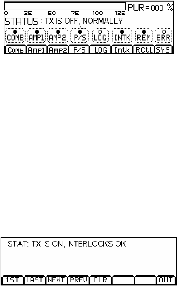
From the Main Menu, the status of the amplifier is displayed and shows if the amplifier is ready for operation.
Status legends, when lit, such as the INTK (INTERLOCK), usually signify OK conditions and that the transmitter is
ready to be switched ON.
Check that all of the following conditions are met:
1. Modulator and the up-converter, or Channel Processor are ready.
• Usually in the application of AC, the modulator goes through its warm-up sequence. When all of the red
LEDs are extinguished (not lit), it means that the modulator or up-converter is ready.
2. POWER METERING is at Zero.
• On the LCD (see Main Menu display in Error! Reference source not found.5), the PWR should be at
000% and the STATUS should be TX IS OFF, NORMALLY.
3. MXi MAIN CONTROLLER is ready.
• If there were prior faults, clear them by pushing the RESET button on the power supply chassis front
panel.
4. INTERLOCKS are closed or OK.
• Interlocks and Status are OK.
Figure 6 Interlocks Status
5. AGC control is DISABLED at this time.
• Remove the AGC jumper from the control board.
6. The Amplifier is in LOCAL mode.
• Push the REM button so that it is NOT lit.
7. The TX is OFF.
• Push the Front Panel ON/OFF button so that it is NOT pushed in.
4.4 AMPLIFIER ON SEQUENCE
Upon depressing the ON button, the fans start and at the same time the +32V power supplies are enabled, thus
applying B+ to both amplifies. Since the modulator/up-converter or Channel Processor are on hot standby (RF is
always applied), the amplifiers normally produces 100% output power immediately. For first time installations, it is
recommended that the level of the modulator be set to minimum initially and then increase in steps until 100%
power is attained. This is done so that catastrophic failure is avoided. Keep in mind that in a newly installed
PUB07-016 Rev 1 July 12, 2007 07-016-8 MXi802U Operations and Maintenance
transmitter that loose or bad connections in the output, as an example, is possible particularly when the output
system is not swept for proper matching or VSWR. Hence, as the power is increased, by observing the combined,
single amplifier, reflected, and reject power meterings one will be able to assess if everything is in proper order.
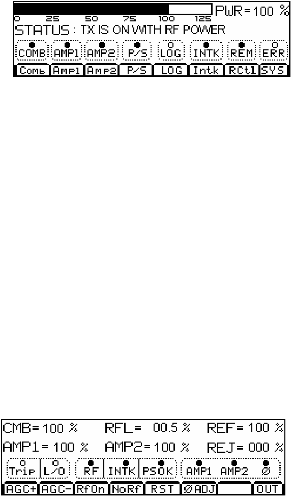
4.4.1 Turning ON the MXi Transmitter
1. Enable amplifier LOCAL operation by pressing the REM touch button such that the REM legend is NOT lit.
• Push the front panel ON button.
• The MXi Amplifier should now be ON.
Figure 7 Transmitter ON
2. Monitor both +32V power supply voltages and currents on the LCD. Check that the power supplies are
operating by pressing the P/S touch button. The voltage readings should be about 30V and the currents should be
about 11A under Static condition (no RF drive).
ALLOW THE AMPLIFIER SOME WARM-UP TIME!
Only after the transmitter has been ON for approximately 15 minutes should you perform the fine
adjustments. The amplifiers must be allowed to reach their operating temperature for stable operation. The
Power Amplifiers in the MXi transmitter are equipped with thermal compensation circuits, which reduce the
output power when the temperature rises. Therefore, the operating temperature must be reached before
adjusting the RF level to its proper level, i.e. 100%. The amplifiers are also equipped with Automatic Gain
Control, primarily designed to prevent the transmitter from overpower or overdrive condition.
3. Increase the RF output by slowly turning the Modulator/Exciter or Channel Processor output level control.
Stop at about 25% output power indicated on the LCD. At this level, the current should not be more than 35
Amps per amplifier.
4. If the current is not drastically higher, increase the power to 50%. Again, make note of the PS current
readings. The current should be less than 50 Amps per amplifier. Proceed to the next step if this condition is
met.
5. Increase the RF output to 100%. The current should be about 60A per amplifier with a black video signal.
Typically, with a 50% APL video signal, the current drawn is about 50A.
6. AGC SETTING: With the AGC still disabled, increase the output power to 110%, using the output level control
in the Exciter or Channel processor. Enable the AGC by inserting the AGC jumper, E16, on the control board.
Use the LOWER button on the LCD to set the power to 100%.
Figure 8 AGC Adjustment
7. With the amplifiers fully functional and adjusted to its final setting, record keeping becomes very important.
Record the current, voltage, power, etc. This data can be used as a very valuable troubleshooting tool later.
Below is typical test data pertaining to the MXi amplifier at 100% output power.
PUB07-016 Rev 1 July 12, 2007 07-016-9 MXi802U Operations and Maintenance
4.4.2 TYPICAL DATA read on the LCD
Combined
COMB 100% RFL 0.5%
AMP1 100% AMP2 100%
Amplifier
FWD 100% RFL 00.2%
AGC 1.0V CUTB 0.0V
Power Supply
PS1 VOLTS 30.0V PS2 VOLTS 30.0V
PS1 CURR 58.0A PS2 CURR 58.0A
PUB07-016 Rev 1 July 12, 2007 07-016-10 MXi802U Operations and Maintenance
5 TEST AND TROUBLESHOOTING
5.1 BENCH TEST PROCEDURES
The following procedures are test instructions for the amplifier modules comprising the MXi amplifier.
5.1.1 Front-End Module, 21B1473, Bench Test Procedure
• Connect a +32V power supply to E1.
• Apply a 0dBm (1mW) RF input to the amplifier.
• Turn RV2 fully clockwise. The front-end should have a gain of 9dB. Adjusting R25 from one extreme to
the other should vary the gain by 4dB.
• RF Mute Check: Connect a variable supply to J3-2. Gradually increase the voltage until the gain drops by
30dB or more. The applied voltage should be approximately 2.5 volts.
• Reflected Power Cutback Check: Connect the variable supply to J4-9. Increase the voltage gradually until
the gain drops by 30dB or more. The voltage should be approximately 4.0 Volts ±0.2V. This same voltage
should also be present at J3-14. J3-6 should be 4.0 volts.
• Overdrive Cutback Check: Connect the variable supply to J3-7. Increase the voltage until the gain drops
by 30dB or more. The voltage should be 7.0 volts ±0.5V. The voltage at J3-11 should be the same and
the voltage at J3-7 should be 4.0 volts.
• Set an adjustable power supply to 2.0 volts. Connect this voltage to J4-1, J4-3 and J4-5 simultaneously.
J2-6 and J3-5 should be high. Disconnecting any one or more of J4-1, 3 or 5 should cause both J2-6 and
J3-5 to go low (0V).
5.1.2 IPA1, 21B1324, Bench Test Procedure
This amplifier must be mounted on a properly sized heatsink for testing.
• Connect a suitable load to the output of the Front-End module.
• On the unit under test (IPA), set RV200 fully clockwise and set RV110 fully counter-clockwise.
• Set variable power supply to 32.0 volts and set its current limit to 1 ampere.
• Apply the +32V to the feed-through capacitor of the pre-amp shield box.
• Adjust RV3 to achieve 6.5 ±0.2 volts at the junction of R5 and RV100.
• Adjust RV200 to achieve total current draw of 500 ±20 mA.
• Check that the junction of R100 and CR100 measures between 3.5 and 5.5 volts.
• Adjust RV110 to raise total current draw to 1000 ±50 mA.
• Check that the junction of R110 and CR110 measures between 3.5 and 5.5 volts.
• Increase the power supply current limiting to 2.2 Amps.
• Increase RV3 clockwise slowly and check that the maximum current limits itself at 1.6 ±0.1 Amp but do
not allow current to go above 2 amps while performing this test.
• Reset RV3 to achieve 6.5 ±0.2 volts measured at the junction of R5 and RV100.
• Check balance of the two transistors with a voltmeter connected between the hot sides of C105 and
C115; the difference in voltage should be less than 3mV.
• Apply RF drive (max. +18 from a pre-amp) and adjust C101, C103, C111, and C113 for minimum
frequency response ripple and flat response. Gain should be a minimum of 15dB with maximum variation
less than 0.5dB over the frequency range 470MHz through 860MHz (Note: output will then be about
+33dBm or 2 Watts for an input of +18dBm, so make sure you properly protect your test equipment).

PUB07-016 Rev 1 July 12, 2007 07-016-11 MXi802U Operations and Maintenance
• If roll off at the higher frequencies prevents meeting this gain-bandwidth specification, it may be
necessary to replace either C103 or C113 or both with a higher value; use variable capacitor made by
Johanson, part # 16E2320-2, which is 2.5 to 10pF.
5.1.3 Driver Pallet, 21B1639, Bench Test Procedure
• BIAS SETTING: Connect a 50-Ohm load to the output of the pallet.
• Before applying +32V to the module, adjust R12 fully clockwise. Limit the power supply current to 3.0A.
• Apply +32V to the B+ terminal. Monitor the current and adjust R12 counter clockwise (CCW) for a total
current of about 2.0A + 0.1A.
• Still monitoring the current, adjust R11 for the current to be at minimum, i.e. current dipping at 1.9A. This
procedure balances the current drawn by the devices, therefore, R11 should not be adjusted again unless
one or both transistors are replaced. Any bias adjustment required from here on should be done using the
overall bias adjustment, R12.
• Readjust R12 to 2.0A. This setting is an initial bias setting and may vary depending on the pallet’s
application. On analog transmitters, this adjustment is used to optimized the inter-modulation products as
well as the system linearity.
• Proceed to the next step if a network analyzer or similar equipment is available.
• RF SWEEP: Adjust C7 for best frequency response. With the bias set at 2.0A, the gain in the frequency range
of 470MHz to 860MHz should be 14 to 16dB.
5.1.4 PA Pallet 11A2142G1 Bench Test Procedure
• BIAS SETTING: Connect a 50-Ohm load to the output of the pallet.
• Before applying +32V to the module, adjust R11 fully counter-clockwise. Limit the power supply current to
3.0A.
• Apply +32V to the B+ terminal. Monitor the current and adjust R11 clockwise (CW) for a total current of
2.0A + or – 0.2A.
• Proceed to the next step if a network analyzer or similar equipment is available.
• RF SWEEP: Adjust C4 for best frequency response. The gain, in the range of 470MHz to 860MHz, should be
between 15 to 16dB.
PUB07-016 Rev 1 July 12, 2007 07-016-12 MXi802U Operations and Maintenance
5.2 BASIC TROUBLESHOOTING TECHNIQUES
One of the best tools in troubleshooting is knowing what the nominal figures or typical values of the MXi amplifier
when it is at its normal performance. If a fault condition occurs, then you can compare the data taken previously
with the present conditions and come up with a reasonable conclusion about what is at fault.
The following describes some fault conditions and possible solutions.
5.2.1 No RF Output
• Check for proper power supply voltage and current
• Check for the presence of video signal to the modulator
• Ensure the modulator IF carrier switches are ON.
• Check for potential connector problems causing either no drive to a module pallet (input connector) or VSWR
(output connector) problems.
• Check the fuses on the driver stages.
5.2.2 Output Reduced to 25%
If the output is approximately 25%, a possible cause is a total loss of power from one of the amplifiers. The
Mxi802 transmitter utilizes a 3dB combiner to combine the power of the two RF amplifiers. If one amplifier
produces no output, half of the output of the operating amplifier goes to the output and the other half goes into the
reject loads. Similarly, most of the stages in the amplifier have redundancy built in them so that if one fails the
output of that stage will be reduced to quarter power (25%). A measurement of the current drawn by the amplifier
will determine if this condition exists. The IPA usually draws 1A. If the current is 0.5, then this is the case.
Similarly, the Driver or PA pallet draws 2.0A with no drive condition. If it reads 1.0A, then this is the case, also.
PUB07-016 Rev 1 July 12, 2007 07-016-13 MXi802U Operations and Maintenance
6 MAINTENANCE
Equipment which is regularly and carefully maintained is far less likely to be subject to sudden failure than that
which is operated without regard to basic maintenance requirements. A detailed preventive maintenance program
should be established to ensure that the original efficiency and picture quality is maintained throughout the life of
the equipment. Given reasonable care and attention, the transmitter will provide efficient and reliable service for
many years.
Preventive maintenance techniques do not necessarily involve extensive dismantling of the various assemblies;
on the contrary, this practice is to be discouraged unless a valid reason exists for doing so. Preventive
maintenance is more directed at detailed physical inspection and the general observation of the equipment during
and after operation, to detect the presence of any abnormality, which, if not corrected, might result in operational
failure.
In preparing any maintenance program, the frequency and scope of the inspections must be determined and to a
great degree will be influenced by site location and the station's market parameters and consequently its hours of
operation, equipment configuration, and technical personnel deployment. For example, is the station on the air for
24 hours-a-day? Are there main/standby transmitters and are they attended or unattended?
In general, the following routines should form the basis of any maintenance program.
6.1 DAILY
At an attended site, the operator is afforded the opportunity to make frequent checks on the equipment and
thereby increase his/her familiarity with its operation. The transmitter log entries made during these checks would
include all meter readings, also any irregularity in performance or in picture quality, for later analysis. An
unattended site where equipment is operated by remote control and monitored by telemetry and a high quality off-
air receiver or demodulator can also be continuously checked for performance by studio technical personnel.
6.2 MONTHLY
In addition to the normal operational tests, thorough physical inspection of every piece of equipment should be
made, with all power turned off. All surfaces should be dusted off or wiped down, terminal boards checked for
loose connections, and all components examined for any evidence of overheating. Air filter media should be
inspected and replaced if necessary. High-pressure air, not over 20psi, can be used with discretion to dislodge
dust from inaccessible places.
6.3 SEMI-ANNUALLY AND ANNUALLY
Check all external RF connections for tightness, looking specifically for any discoloration, which might indicate a
loose inner connector, flange or sleeve coupling. Test the passive RF system with a transmission test set or
network analyzer, if one is available, to identify any potential problems with the antenna or line. Inspect and clean
contacts on all switches and contactors; carefully redress contact surfaces if pitted.
Check the operation of all interlocks including patch panel, dummy load, air and thermal switches and emergency
interlocks (if applicable).
6.4 TRANSMITTER COOLING SYSTEM
All cooling fans in the transmitter are fitted with sealed bearings requiring no lubrication during the lifetime of the
motor. Access to the fan assembly is via the bottom of the transmitter.
PUB07-016 Rev 1 July 12, 2007 07-016-14 MXi802U Operations and Maintenance
7 SERVICE
The MXi contains few user-serviceable parts; the modular surface-mount design makes module replacement
and/or factory repair the most efficient repair method.
The service most likely to be performed by users is the replacement of the fan array.
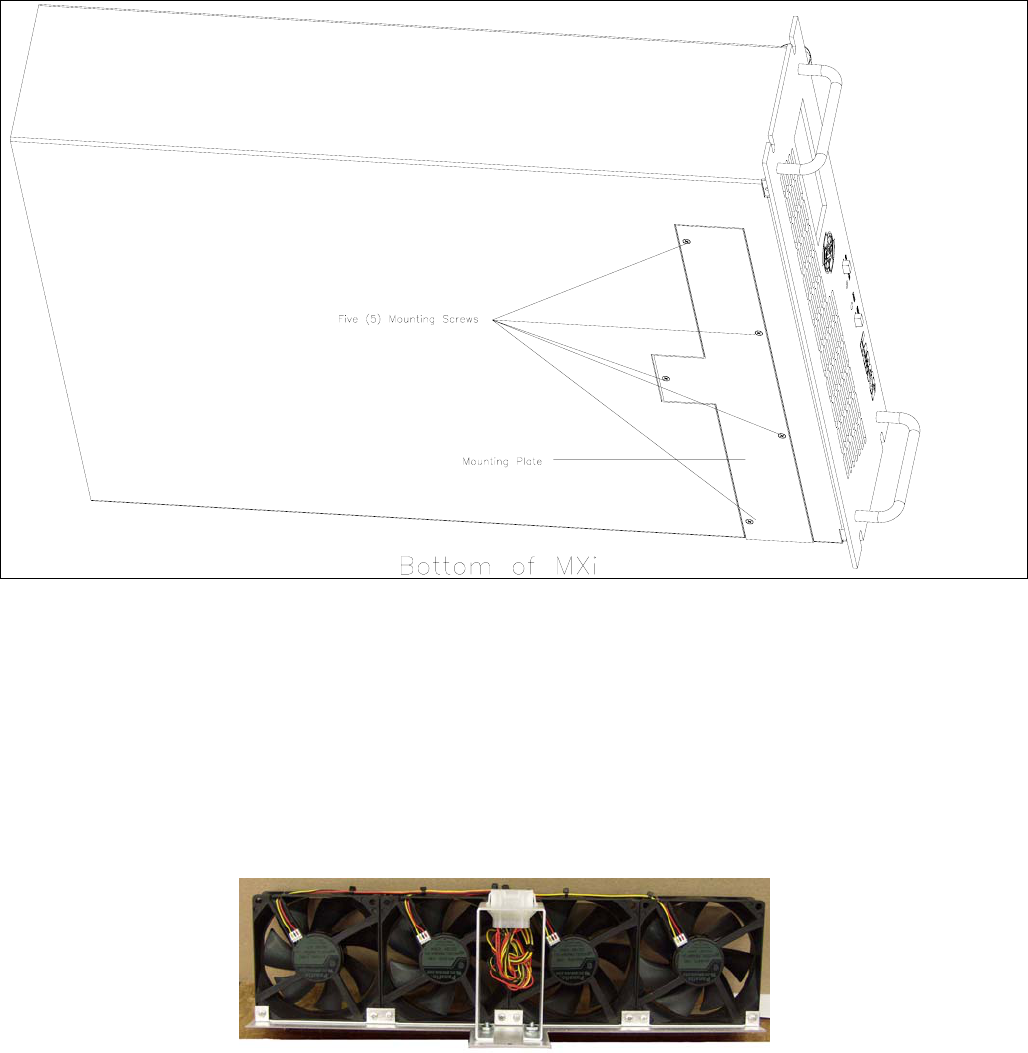
7.1 REMOVING THE FAN ARRAY
The MXi fan array consists of four 4” muffin-type fans which are attached to the mounting plate. The mounting
plate is secured to the bottom of the MXi chassis with five Phillips head screws.
Figure 9 Bottom View of MXi
1. Turn the MXi OFF.
2. Disconnect the AC power from the MXi.
3. Slide the MXi partially out from the mounting rack. Important: Ensure that the weight of the MXi is fully
supported.
4. With a Phillips screwdriver, remove the five mounting screws on the underside of the MXi. When
removing the last screw, be sure to hold the mounting plate in place.
5. Remove the mounting plate. The fan array is attached to the mounting plate and comes out with the plate.
Figure 10 Fan Array
PUB07-016 Rev 1 July 12, 2007 07-016-15 MXi802U Operations and Maintenance
7.2 REPLACING THE ENTIRE FAN ARRAY
In the event of a fan failure, LARCAN recommends replacing the entire array, as all fans have a similar lifespan.
1. Remove the fan array as described in Section 7.1.
2. Slide the new fan array into the MXi. The power connection is aligned so that it connects when the
mounting plate is fully in place.
3. Insert and tighten the five mounting screws. Note: Screws only need to be snug; do not overtighten.
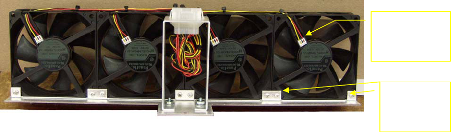
7.3 REPLACING A SINGLE FAN
1. Remove the fan array as described in Section 7.1.
2. Each of the four fans is attached to the mounting plate via two screw-and-nut assemblies. Remove the
screws and nuts and set aside.
Figure 11 Fan Attachment to Mounting Plate
3. Disconnect the three-pin wiring harness connection by gently sliding it back with a fingernail or small
plastic tool.
4. If necessary, carefully cut and remove the zip tie holding the wires to the fan frame.
5. Remove the defective fan and replace with a known good fan of exactly the same dimensions and
specifications.
6. Re-connect the three-pin wiring harness connection.
7. Re-fasten the two screw-and-nut assemblies holding the fan to the mounting plate.
8. If necessary, replace the zip tie holding the wires to the fan frame.
9. Replace fan array into MXi as described in Section 7.1.
Screw-and-
nut
assemblies
Three-pin
wiring harness
connector
MXi802U OPERATIONS AND MAINTENANCE
PUB07-016 Rev 1 July 12, 2007 07-016-16 MXi802U Operations and Maintenance
8 TEST EQUIPMENT SETUP
Figure 12 Test Equipment Setup
MXi802U OPERATIONS AND MAINTENANCE
PUB07-016 Rev 1 July 12, 2007 07-016-17 MXi802U Operations and Maintenance
9 SPECIFICATIONS
Specifications are subject to change without notice.
9.1 ELECTRICAL
AC Line Input ...................................................................................................................190 to 264VAC, 50 to 60Hz
Power Consumption, black picture + 10% aural ............................................................................... 4000VA (typical)
9.2 ENVIRONMENTAL
Ambient Temperature .....................................................................................................0°C to +45°C (0°F to 113°F)
Humidity ..................................................................................................................................................... 0% to 90%
Altitude ..............................................................................................................................................2286 m (7500 ft)
9.3 COOLING
Four 4” muffin fans per amplifier push air through the heatsinks and through the rear panel perforations.
9.4 DIMENSIONS
The Amplifiers, Power Supply, IF Modulator, and Up-converter chassis are standard 19" rack wide units.
Height
Amplifiers and Power Supply......................................................................................................15.75" (9RU)
I.F. Modulator................................................................................................................................1.75” (1RU)
Up-converter.................................................................................................................................1.75” (1RU)
Total Height ..............................................................................................................................19.25” (10RU)
Depth is 31" to the back of the 2-way combiner.
9.5 SHIPPING WEIGHT
Weight
Amplifier (each) ……………………………….……… ...........................................Approximately 17kg (37lbs)
Power Supply ……………………………….……… ..............................................Approximately 18kg (40lbs)
2-Way Combiner ……………………………….……… ..........................................Approximately 3.6kg (8lbs)
Total Weight ……………………………….……… ..............................................Approximately 55kg (122lbs)
MXi802U AMPLIFIER CHASSIS
PUB07-011 Rev 0 January 9, 2007 07-011-i MXi802U Amplifier Chassis
CONTENTS
1 MXi802U AMPLIFIER.....................................................................................................................................................1
FIGURES
FIGURE 1 FRONT VIEW OF MXI802U AMPLIFIER .........................................................................................................................1
FIGURE 2 REAR VIEW OF MXI802U AMPLIFIER ...........................................................................................................................1
FIGURE 3 MXI FAN ARRAY ..........................................................................................................................................................2
FIGURE 4 MXI AMPLIFIER INTERIOR ............................................................................................................................................2
FIGURE 5 41D2168 MXI401/802 AMPLIFIER WIRING SCHEMATIC SHT1 REV 0 ...........................................................................3
MXi802U AMPLIFIER CHASSIS
PUB07-011 Rev 0 January 9, 2007 07-011-1 MXi802U Amplifier Chassis
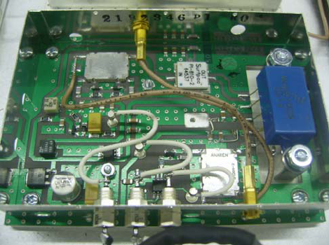
1 MXi802U AMPLIFIER
The MXi802U Amplifier Chassis Assembly 41D2101G4 consists of a standard 19" rack mountable 5.25" (3RU)
enclosure containing the amplifier heatsink assembly, a fan array assembly consisting of four DC cooling fans, a
controller board with built-in RF detectors, and a rear panel assembly with connectors for interfacing to external
equipment. Figure 1 is a front view of the MXi802U amplifier.
Figure 1 Front View of MXi802U Amplifier
Figure 2 Rear View of MXi802U Amplifier
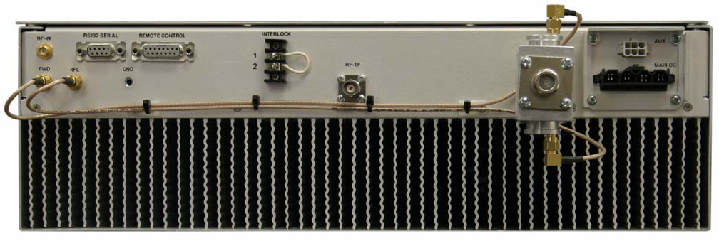
The rear of the MXi802U AMPLIFIER has the following connectors (from left to right):
• RS232 SERIAL nine-pin connector
• REMOTE CONTROL 15-pin D-shell connector
• RF IN SMA connector
• INTERLOCK terminal board
• RF TP SMA connector – RF sample
• RF OUT N connector
• 12V 6-pin connector
• 28V 4-pin connector
The MXi802U is classified as a broadband amplifier, thus it is operational to cover the entire UHF television
spectrum ranging in frequencies from 470MHz to 860MHz.
Controlled DC power to the amplifier assembly comes from the high efficiency 2000W switching power supply via
a 32V four-pin connector. Regulated DC of 32V from the switching power supply is the B+ voltage to the amplifier
heatsink assembly. The second auxiliary output of the power supply is +12VDC, which is used for powering the
controller and the cooling fans.
The heatsink cooling fans are the +12VDC, 4-inch muffin model. Typically, they come ON at the same time B+ is
applied to the power amplifier. The voltage is supplied to the amplifier from the 12V six-pin connector on the rear
panel and it is connected to the controller PC board connector, J8. As built, the cooling fans push air from the
MXi802U AMPLIFIER CHASSIS
PUB07-011 Rev 0 January 9, 2007 07-011-2 MXi802U Amplifier Chassis
front panel through the heatsink and through the perforations in the rear panel. This assembly is located
underneath the MXi Controller board.
Figure 3 MXi Fan Array
A thermal switch is mounted on the heatsink where the operating temperature is sensed. If this temperature
increases beyond the trip point of the thermal switch, which is about 76°C, its contact opens and breaks the
interlocking circuit of the MXi amplifier. The interlock circuit ultimately controls the power supply to the power
amplifier and therefore shuts down and remains OFF until the heatsink cools down to about 60°C.
Figure 4 MXi Amplifier Interior
A directional coupler is built into the 4-way combiner mounted at the rear of the heatsink and provides forward
and reflected RF signals to the controller. These RF samples are detected and processed on the MXi controller to
provide DC outputs corresponding to these signals. They are then used for AGC, VSWR supervision and this
information is also sent serially through the RS-232 connection to the main controller located inside the power
supply chassis.
The chassis is wired according to the functional diagram 41D2168 as shown in Figure 5.
MXi401/802U POWER AMPLIFIER HEATSINK ASSEMBLY
PUB07-027 Rev 1 July 17, 2007 07-027-i MXi401/802U Power Amplifier Heatsink Assembly
CONTENTS
1 POWER AMPLIFIER HEATSINK ASSEMBLY 40D2104G1.....................................................................................1
2 FRONT END MODULE ASSEMBLY 21B1473G1........................................................................................................2
3 IPA MODULE 21B1951G1...............................................................................................................................................3
4 DRIVER MODULE 21B1639G1......................................................................................................................................5
5 PA PALLET ASSEMBLY 11A2142G1 ...........................................................................................................................6
6 FOUR-WAY SPLITTER 21B2425G1..............................................................................................................................7
7 FOUR-WAY COMBINER 21B2426G1...........................................................................................................................8
FIGURES
FIGURE 1 MXI SUB-ASSEMBLIES .................................................................................................................................................1
FIGURE 2 FRONT END MODULE....................................................................................................................................................2
FIGURE 3 IPA MODULE ................................................................................................................................................................3
FIGURE 4 DRIVER MODULE ..........................................................................................................................................................5
FIGURE 5 PA PALLET ASSEMBLY .................................................................................................................................................6
FIGURE 6 FOUR WAY SPLITTER....................................................................................................................................................7
FIGURE 7 FOUR WAY COMBINER .................................................................................................................................................8
FIGURE 8 MXI AMPLIFIER REAR PANEL.....................................................................................................................................11
FIGURE 9 21B1473 MXI FRONT END UHF DTV DRIVER ASSEMBLY SHT1 REV 5.1..................................................................12
FIGURE 10 11A1354 MXI FRONT END UHF DTV DRIVER SCHEMATIC SHT1 REV 2.1...............................................................13
FIGURE 11 21B1950A1 IPA FINAL ASSEMBLY SHT1 REV 2.......................................................................................................14
FIGURE 12 21B1950S1 IPA SCHEMATIC DIAGRAM SHT1 REV 0.1 .............................................................................................15
FIGURE 13 21B1639S DRIVER PALLET SCHEMATIC SHT1 REV 5................................................................................................16
FIGURE 14 11A2142A1S PALLET CIRCUIT SCHEMATIC SHT1 REV 3..........................................................................................17
FIGURE 15 21B2425A1 4 WAY SPLITTER ASSEMBLY SHT1 REV 0 .............................................................................................18
FIGURE 16 21B2425S1 4 WAY SPLITTER SCHEMATIC SHT1 REV 0 ............................................................................................19
FIGURE 17 21B2426A1 4 WAY COMBINER ASSEMBLY SHT1 REV 2...........................................................................................20
FIGURE 18 21B2426S1 4 WAY COMBINER SCHEMATIC SHT1 REV 2 ..........................................................................................21
MXi401/802U POWER AMPLIFIER HEATSINK ASSEMBLY
PUB07-027 Rev 1 July 17, 2007 07-027-1 MXi401/802U Power Amplifier Heatsink Assembly
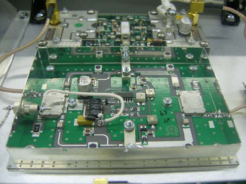
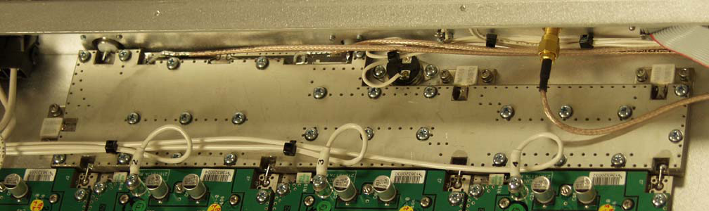
1 POWER AMPLIFIER HEATSINK ASSEMBLY 40D2104G1
The MXi Power Amplifier Heatsink Assembly 40D2104G1 consists of a fan-cooled heatsink and nine printed
circuit board sub-assemblies. The first module is a pre-amplifier, known as the Front-End Module, then the
Intermediate Power Amplifier, IPA. These first two stages are Class A amplifiers. Next is the Driver pallet, which is
biased so as to pre-correct for the non-linearity in the final amplifier stage. The next stage is the four way splitter
that splits the RF power so it can be fed to the PA pallets. The final amplifier stage is the PA pallets, which are
capable of delivering over 125W Analog power each. The last sub-assembly on the heatsink is the four way
combiner which combines the output power from the PA pallets. Also mounted on the heatsink is a thermal
switch, which protects the amplifiers from over-temperature conditions such as the absent of cooling or amplifier
over dissipation. This heatsink assembly is mounted in the Amplifier Chassis Assembly 41D2101G1. Descriptions
of each stage are detailed in the following pages.
Figure 1 MXi Sub-Assemblies
The above picture illustrates the arrangement of the sub-assemblies on the amplifier heatsink assembly. From
right to left are the Front-End, IPA and Driver modules. Centered and towards the back are the Splitter, PA
modules and the Combiner. Strategically installed on the heatsink, is a thermal switch which protects the amplifier
from over temperature conditions.
Cooling for the heatsink is provided by a fan array assembly consisting of four 4-inch axial flow +12VDC muffin
fans. This array is situated near the front section of the MXi housing underneath the MXi Amplifier Controller PC
board. The fans blow air into the finned portion of the heatsink, which exhausts through the rear.
MXi401/802U POWER AMPLIFIER HEATSINK ASSEMBLY
PUB07-027 Rev 1 July 17, 2007 07-027-2 MXi401/802U Power Amplifier Heatsink Assembly
2 FRONT END MODULE ASSEMBLY 21B1473G1
The front end module performs several distinctive functions. Firstly, it serves as a pre-amplifier, which boosts the
signal from the up-converter by approximately 9dB. This module also contains a phase shift circuit and a variable
attenuator; both adjustments are available and set to maximum and do not need to be adjusted in the MXi
amplifier. These circuits are only used for adjusting phase and gain balance between two paralleled amplifiers.
Figure 2 Front End Module
The RF signal is fed to the amplifier through hybrid HY1 and attenuator P-AT1. Refer to Figure 10.
HY1, along with associated components CR1, CR2, C1 through C6, R1, R2 and RV1 act as a phase shifter. P-
AT1 is a variable attenuator. The attenuation is controlled by RV2. Typically, RV2 is adjusted for minimum
attenuation (fully clockwise) during the bench testing of the module. Once this is done, RV2 is not adjusted again.
U1 is a hybrid linear amplifier with a nominal gain of 17.5dB. The typical operating point of the amplifier in this
application is well below the 1 Watt rating of the hybrid.
The power to the Front-End module (+32VDC) comes in at TP2.
The control voltage at TP1 comes from the AGC and VSWR cutback circuit in controller board. This voltage
corresponds to the output power of the final amplifier. If the AGC circuit is enabled and the output power tries to
increase, TP1 voltage increases, thus maintaining the output at the pre-set level. Similarly, if the reflected power
increases past the VSWR cutback setting, TP1 increases and the output power is reduced.
The higher the voltage at TP1, the higher the attenuation in the module, therefore, lower the overall output power.
RF STATUS (TP3) and as mentioned above the PHASING control (RV1) and GAIN control (RV2) are other
features of this module which are not applicable to this amplifier.
MXi401/802U POWER AMPLIFIER HEATSINK ASSEMBLY
PUB07-027 Rev 1 July 17, 2007 07-027-3 MXi401/802U Power Amplifier Heatsink Assembly
3 IPA MODULE 21B1951G1
The Intermediate Amplifier 21B1951G1 consists of two FET amplifiers, type MRF181, paralleled in RF phase
quadrature and operated in Class A. Amplifier static bias control and over-current protection is provided by an
industry-standard type µA723 regulator IC, U1. The overall gain of the pre-amplifier is a nominal 15dB over the
UHF band. Refer to Figure 12.
Figure 3 IPA Module
The input signal is split evenly by quadrature hybrid splitter HY1. Each FET gate is matched with the equivalent of
an L network followed by a π network. Capacitors C100 and C110 provide DC blocking of the gate voltage. A
couple of low impedance microstripline sections along with adjustable capacitor (C101 or C111) to ground and the
gate capacitance of the FET form the L-C-L-C matching network for the input circuit. This matching arrangement
is good for operation from 470 through 860MHz, adjustable capacitors C101 and/or C111 provide for a flat
frequency response over the range.
The output circuit is similar except it uses narrower (higher impedance) microstriplines because the drain
impedance of the FET is higher. The output-matching network is adjustable with variable capacitor C103 or C113.
Again, this capacitor is adjusted only to provide flat response over the 470 to 860MHz range. An output coupling
capacitor C104 or C114 completes the match to 50 ohms; two amplifier outputs are combined in a quadrature
hybrid HY2.
Bias to the gates of the FETs passes through R100 or R110 from balance controls RV100 or RV110. The bias
regulator Ul uses an µA723 (MC1723CD) to provide approximately 6.5 volts to the gate bias controls RV100 and
RV110. Voltage divider R5, R6 provides the inverting input of the regulator error amplifier with a sample of the
output voltage and the wiper of RV3 provides the non-inverting input with its reference signal, which is an
adjustable fraction of the 7.15 V built-in reference of the µA723. The adjustment of RV3 should therefore be able
to give an output within the range from zero to approximately 9 volts. R4, C2, C1, R3, and C4 provide frequency-
compensation and maintain regulator stability.
Drain current of the two FETs is sampled by the voltage drop across R7. When this voltage exceeds
approximately 0.5V at normal operating temperature (about 1.5 amps total FET current), Q3 begins conduction
and feeds voltage to pin 2 of the regulator to start its current foldback/limiter circuit. The regulator reduces its
output voltage which in turn reduces the bias on the FETs; they decrease their drain currents, reducing the
voltage drop across R7 and over-current protection is achieved. CR1 protects Q3 emitter-base junction from
current inrush to C3 and C107 charging during start-up.
Setup is performed during initial factory testing by first setting RV110 to its maximum CCW position so that Q2
receives no bias voltage, therefore should not conduct, then setting RV3 for regulator output at U1 pin 10 to exactly
+6.5 ± 0.2 volts. An ammeter is connected in series with the +32V supply lead. Then RV100 is set for 500mA
reading on the ammeter due to Q1 conduction. Next, RV110 is set for Q2 also 500mA so that Q1 + Q2 = twice as
much current = 1A.
MXi401/802U POWER AMPLIFIER HEATSINK ASSEMBLY
PUB07-027 Rev 1 July 17, 2007 07-027-4 MXi401/802U Power Amplifier Heatsink Assembly
Another (final) check is made before applying RF: gate voltages at C102 and C112 are measured. With good FETs,
both voltages should be approximately equal and in the range +3.5 to +5.5VDC.
Current limiting is checked by increasing the setting of RV3; the current will increase to a threshold of, and must not
exceed, 1.6 amperes. RV3 is then reset to obtain the original +6.5 volts at U1-10.
When RF sweep is applied, C101, C111, C103 and C113 are adjusted for flat response over the range.
The overall gain of the Intermediate Amplifier is a nominal 15dB over the band.
MXi401/802U POWER AMPLIFIER HEATSINK ASSEMBLY
PUB07-027 Rev 1 July 17, 2007 07-027-5 MXi401/802U Power Amplifier Heatsink Assembly
4 DRIVER MODULE 21B1639G1
The design of the Driver Module 21B16391G1 is based on the device MRF374A. It is a Lateral N-channel
Broadband Push-Pull Power MOSFET capable of power near 100W (rated power). However, for this application
and the desired linear performance, its output to the final stage is about 5W. Refer to Figure 13.
Figure 4 Driver Module
The strip-line balun developed at LARCAN is a practical implementation of the coaxial cable based solution on a
broadside-coupled horizontal stripline structure. It is made up of three printed circuit boards of high dielectric
material bolted together. Using this structure, very tight coupling can be achieved, thus emulating the properties of
a coaxial transmission line balun. With this arrangement, the characteristic impedance and degree of coupling can
be controlled through geometric dimensions. This circuit is the subject of a patent application.
Components C6 through C11 and C52, along with the associated printed circuit traces, form the matching
network to the gate of the push-pull transistor Q1. L2 and R2 along with L3 and R3 are low frequency parasitic
arrestors. Similarly, C14 through C15 and C53 along with associated stripline traces provide output matching on
the drain of the device. C6, C8, C16 and C18 also provide DC blocking of the supply and bias voltage. C7 is
factory adjusted for a flat frequency response from 470 to 860MHz.
DC power enters the module through a screw terminal connection and is fed to the main circuit board through a
series of jumpers. +32VDC is fed to the drains of the FETs via L5 and L6 with bypass capacitors C13, C25, C20,
C22 and C28. Bias for the devices is via L1/L4 with bypass capacitors C1, C2, C5 and C12. The bias voltage is
adjusted via R12 and R11, from a regulated source provided by Ul. R12 sets the overall bias and R11 provides
adjustment for balance between Q1 and Q2. Thermistors R21 and R22 provide thermal stability for the bias.
MXi401/802U POWER AMPLIFIER HEATSINK ASSEMBLY
PUB07-027 Rev 1 July 17, 2007 07-027-6 MXi401/802U Power Amplifier Heatsink Assembly
5 PA PALLET ASSEMBLY 11A2142G1
Drawing reference: Figure 14
The Power Amplifier pallet is a FET amplifier assembly containing a stripline balun system. The baluns are used
for impedance matching and coupling signals at the input and output of the pallet. It is a practical implementation
of the coaxial-based solution on a broadside-coupled horizontal stripline structure. It is made up of two circuit
boards fabricated using high dielectric constant material. Using this structure, a very tight coupling can be
achieved, thus emulating the properties of a coaxial transmission line balun. With this arrangement, the
characteristic impedance and degree of coupling can be controlled through geometric dimensions.
Figure 5 PA Pallet Assembly
The amplifier circuit is based on the Laterally Double-Diffused MOSFET, Q1.
Capacitors C2, C3, C4, C8 and C33 along with the associated printed circuit traces, form the matching network to
the gates of Q1. C4 is factory adjusted for a flat frequency response. Similarly, C12 through C15 and C28 along
with associated stripline traces provide output matching on the drain of the device. C3, C8, C14 and C15 also
provide DC blocking of the supply and bias voltage.
DC power (between +28VDC and +32 VDC, depending on the application) enters the module through a screw
terminal connection. This DC voltage is fed to the drains of the device via L1 and L2 with bypass capacitors and
C16 to C27. Bias for the devices is via R8 and R5 with bypass capacitors C5 to C7 and C9 to C11.
The bias circuit is located on the 11A2142 board at the input side of the pallet. It provides two functions; precision
gate bias setting and external shutdown. The pallet's shutdown function is used in certain applications where the
pallet is used as a driver amplifier.
The bias voltage is adjusted using R11 from a regulated source provided by U1. Thermistor R18 provides thermal
stability for the bias.
The source of the bias voltage is a reference IC, U1, which has it's ground reference terminal connected to the
collector of Q5. Q5 is biased using R10 and R16 to provide thermal compensation.
When no Shutdown (5V) is applied at R1, the precision reference is active and provides 6.2VDC to the level
adjustment circuit R21, R11 and R17. When R11 has been set to achieve 2A bias current to the pallet, a bias
voltage of approximately 3.6 to 3.8VDC is applied to the gates of the FETs.
MXi401/802U POWER AMPLIFIER HEATSINK ASSEMBLY
PUB07-027 Rev 1 July 17, 2007 07-027-7 MXi401/802U Power Amplifier Heatsink Assembly
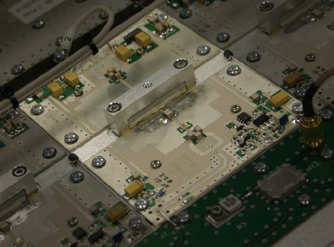
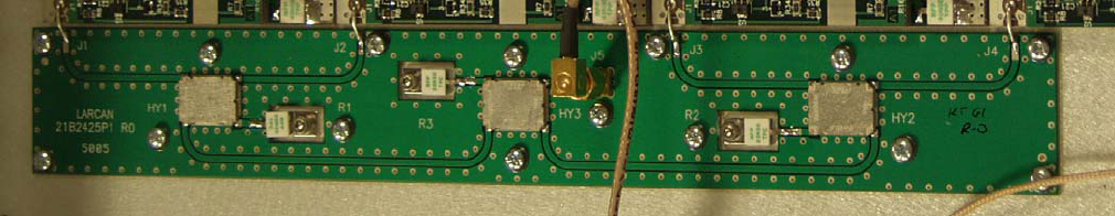
6 FOUR-WAY SPLITTER 21B2425G1
Drawing reference: Error! Reference source not found.5 and Figure 16
The splitter utilizes 4-port 3dB quadrature (90° phase difference) hybrid couplers that require a termination on the
4th port. The termination maintains isolation between the two output ports.
The splitter provides four equal amplitude signals to the pallet amplifier inputs with the proper phase relationship
so that the combiner will provide a single output at the desired connector. Any phase and / or amplitude
differences will result in increased dissipation in the combiner isolation terminations and a corresponding
reduction in output power.
Figure 6 Four Way Splitter
The splitter assembly is constructed on a fiberglass substrate using commercially available 3dB hybrid couplers
(Anaren 1F1304-3). All of the transmission lines are ‘Coplanar Waveguide’ type and are arranged so that all pairs
of lines at the output of each hybrid coupler are identical in length to preserve the phase relationship. Direct
connections are made using short lengths of bus wire soldered between the splitter outputs and each amplifier
pallet input. These short connections minimize the phase errors and reflections that can occur with many cable
interfaces.
RF power enters the splitter at SMA type connector J5. The signal is applied to the input port of HY3 and is split
into two equal power (quadrature phase) signals. One output from HY3 is then applied to the input of HY1 and the
other to HY2. The final result is four equal power signals at J1 through J4, each with appropriate phasing to match
up with the four way combiner. The worst case variation in power level between the highest and lowest output is
on the order of 1dB, with all other output levels approximately midway between these highest and lowest values.
The operating bandwidth of the splitter is 470-860 MHz and is determined solely by the hybrid couplers.
The splitter assembly is constructed on a fiberglass substrate using coplanar waveguide 50 ohm transmission
lines to connect all of the components. The width of this type of transmission line can be set at a particular width
(independent of board thickness to a certain degree) so that it matches up well with the hybrid couplers. The
narrow gap between the transmission lines and the ground plane helps to keep the RF field close to the board
surface. However, the transmission lines are still open and will be affected by any outside influence such as
fingers or tools placed near or on the lines. Please keep this in mind if probing around while the unit is operating.
The four way splitter is designed to comfortably handle 25W average power at the input. The power rating in this
case is limited by the losses in the board material. Each of the hybrid couplers is rated 100W CW when provided
with an adequate heatsink and the terminations are rated 20W each. These terminations provide isolation
between the inputs of each pallet amplifier and would not normally be subject to any RF power. Even if the splitter
was operated completely open circuited, the terminations would still be able to dissipate the full 25W of input
power if necessary.
MXi401/802U POWER AMPLIFIER HEATSINK ASSEMBLY
PUB07-027 Rev 1 July 17, 2007 07-027-8 MXi401/802U Power Amplifier Heatsink Assembly
7 FOUR-WAY COMBINER 21B2426G1
Drawing reference: Error! Reference source not found.7 and Figure 18
The combiner utilizes 4-port 3dB quadrature (90° phase difference) hybrid couplers that require a termination on
the 4th port. The termination maintains isolation between the two input ports. The combiner is wideband and
covers the entire UHF television band from 470MHz to 860MHz.
The combiner is constructed using a stacked arrangement of three separate PCBs. All of the stripline traces are
found on the middle PCB and each hybrid coupler is formed using broadside coupled lines on opposite sides of
the middle board. The two outside PCBs support the ground planes required above and below the stripline.
Cutouts are made in the upper and lower ground plane PCBs to allow access to the connection points on the
middle layer. Direct connections are made using short lengths of bus wire soldered between the combiner inputs
and each amplifier pallet output. These short connections minimize the phase errors and reflections that can
occur with many cable interfaces.
Figure 7 Four Way Combiner
In the four way combiner, the RF power arriving at the four inputs is added at two successive stages and exits the
assembly on a single transmission line. In addition to combining, the assembly also provides a forward RF sample
for monitoring (-58dB nominal).
The combiner is constructed using a sandwich of three separate Teflon-woven fiber PCBs. The two outside
ground plane boards are 1/8” thick and the middle board is 0.020” thick for a total height of nearly 0.28” when the
copper layers are added in. This type of substrate material exhibits very low RF power loss and withstands high
temperatures. This combiner is designed to handle 350W of average RF power.
Transmission lines etched on the middle board are called ‘Stripline’ with this stacked arrangement of boards. The
two outside boards are strictly ground planes and all of the RF circuitry is found on the middle board. The 3dB
hybrid couplers are formed by placing two striplines opposite one another on each side of the middle board. Lines
arranged in this manner are referred to as ‘Broadside Coupled Lines’. Hybrid couplers of this type are fully
symmetrical such that any one of the four ports may be chosen as the output (when used as a combiner) or input
(when used as a splitter). The transmission lines that connect the hybrid couplers are etched on whatever side of
the board is most convenient. Strictly speaking, these transmission lines are called ‘Offset Striplines’ because
they are not fully centered between the ground planes.
When an RF signal within the proper frequency range of the 3dB hybrid coupler is applied to one port of the
coupled lines (assuming all other ports are properly terminated), two equal power (within 1dB) signals appear at
the two output ports. These two signals will have a 90° phase difference, with the mainline output port lagging the
coupled port. The mainline is considered the line with DC connection between the input and one of the output
ports. The coupled port has no DC connection to the input, but does have a DC connection to the termination
resistor. When looking at the 3dB hybrid as a combiner, each of the input ports may be treated separately and
viewed as a splitter. The resulting signals arriving at the output port add because they are equal in amplitude and
phase while the signals arriving at the reject port cancel because they are opposite in phase.
In order for proper combining to take place, all four signals must be present, have the same amplitude, and the
proper phasing. If not, then some of the power will be directed toward one or more of the reject loads, which
purposely dissipate these imbalances. At this point, assume that all four inputs are present, have equal

MXi401/802U POWER AMPLIFIER HEATSINK ASSEMBLY
PUB07-027 Rev 1 July 17, 2007 07-027-9 MXi401/802U Power Amplifier Heatsink Assembly
amplitudes and the proper phasing. Power at combiner input ports J1 and J2 is combined at the output of HY1
and becomes one of the input signals to HY3. The same occurs with the power entering at ports J3 and J4 – it
adds at the output port of HY2 which in turn is connected to the other input port of HY3. The combined power
appearing at the output of HY3 is then directed through a directional coupler before reaching the combined output
port at J5.
The power handling capacity of the combiner is limited by the power rating of the balancing terminations used.
These balancing terminations, or reject loads, are used to absorb power that would otherwise be reflected or
directed toward other amplifier outputs. If an amplifier pallet output power is reduced, or drops to zero (in the case
of DC power removal due to a blown fuse), some power from the remaining amplifiers will be dissipated in the
reject loads. As an example, if the DC power were removed from the amplifier pallet on input J1, then half of the
power at input J2 is directed into reject load R1. This occurs because 3dB hybrid coupler HY1 has only a single
input and now acts as a splitter. As a result of the reduced power at the output of HY1, some power will also be
dissipated in R3. The worst case scenario involves the complete shutdown of a pair of amplifiers with zero power
entering either ports J1 and J2 or ports J3 and J4. The combined power of two of the pallets is applied to one port
of HY3 and no power appears at the second input of HY3. HY3 now acts as a power splitter and directs half of the
power toward the reject termination. As an example, if the RF power from each pallet is 100W, then the power
applied to one input of HY3 would be 200W which would then be divided between the output and reject ports of
HY3. Under these conditions, the reject load would be required to dissipate 100W. The terminations used on the
combiner have an individual power rating of 250W average RF power, but we typically de-rate them by at least
half in order to ensure long term reliability.
The formulas following this paragraph may be used to determine the level of reject power in any particular reject
load based on the input power to that hybrid coupler.
For a single 3dB hybrid coupler: Pout = ½(P1 + P2) + [√(P1P2)]cosθ
Prej = ½(P1 + P2) – [√(P1P2)]cosθ
P1 and P2: power at each input port
Pout: combined output power
Prej: power dissipated in the reject load
Θ: phase error between P1 and P2 (Θ=0 assumed)
Total Output and Reject Power PTout = [1-(n/4)]² x 100%
in a Four Way Combiner: PTrej = 1/4[n-(n²/4)] x 100%
PTout: total combined power at the combiner output port
as a percentage of the rated output power
PTrej: total power dissipated in reject loads expressed
as a percentage of the rated output power
n: number of pallet amplifiers not supplying power to the
combiner
Example: If one pallet amplifier is not supplying power, then n=1 and the power appearing at the combined output
and in the reject loads is as follows:
PTout = [1-(1/4)]² x 100% = 56% (of rated output)
PTrej = 1/4[(1-(n²/4)] x 100% = 19% (of rated output)
MXi401/802U POWER AMPLIFIER HEATSINK ASSEMBLY
PUB07-027 Rev 1 July 17, 2007 07-027-10 MXi401/802U Power Amplifier Heatsink Assembly
It should be noted that the total power (56+19=75%) represents the input power as a percentage of the rated
output power [1-(n/4)] x 100%.
The value of PTrej is the total power dissipated in all of the reject loads. In order to calculate the power in a
particular load, then the formula for a single 3dB hybrid coupler must be used. As an example, assume a total
combined output of 300W average RF power from the combiner and 75W at each input (disregarding losses).
Using the same example as above, assume that no power enters at J1. The resulting power dissipated in R1and
R3 is calculated as follows (assume ideal phasing in all cases cosθ=1): Refer to schematic drawing 21B2426S1
as a guide
HY1: power into J2 = 75W (P1=75)
power into J1 = 0W (P2=0)
Pout = ½(P1 + P2) + [√(P1P2)]cosθ
= ½(75 + 0) + [[√(75x0)]cosθ
= 37.5W
Prej = ½(P1 + P2) – [√(P1P2)]cosθ
= ½(75 + 0) – [√(75x0)]cosθ
= 37.5W
Power into J1+J2 input of HY3 = 37.5W
Power into R1 = Prej = 37.5W
HY2: power into J3 = 75W (P1=75)
power into J4 = 75W (P2=75)
Pout = ½(P1 + P2) + [√(P1P2)]cosθ
= ½(75 + 75) + [[√(75x75)]cosθ
= 150W
Prej = ½(P1 + P2) – [√(P1P2)]cosθ
= ½(75 + 75) – [√(75x75)]cosθ
= 0W
Power into J3+J4 input of HY3 = 150W
Power into R2 = Prej = 0W
HY3: power into J1+J2 input = 37.5W (P1=37.5)
power into J3+J4 input = 150W (P2=150W)
Pout = ½(P1 + P2) + [√(P1P2)]cosθ
= ½(37.5 + 150) + [[√(37.5x150)]cosθ
= 168.8W
Prej = ½(P1 + P2) – [√(P1P2)]cosθ
= ½(37.5 + 150) – [√(37.5x150)]cosθ
= 18.8W
MXi401/802U POWER AMPLIFIER HEATSINK ASSEMBLY
PUB07-027 Rev 1 July 17, 2007 07-027-11 MXi401/802U Power Amplifier Heatsink Assembly
Power at HY3 output = 168.8W
Power into R3 = Prej = 18.8W
As a cross check of the earlier calculations, the total output (168.8W) as a percentage of the output (300W) is
indeed 56%. The total reject power (56.3W = 37.5 + 0 + 18.8) as a percentage of the rated output (300W) is also
correct at 19%.
The combiner also contains a directional coupler which is constructed from edge coupled transmission lines. This
is also a 4 port device similar to the 3dB couplers, except the coupling is much weaker (-40dB nominal in this
case). The input and output port of the directional coupler is the main output 50Ω transmission line, while the
other two ports are the ends of the coupled line. The coupled line is simply a second 50Ω transmission line laying
parallel and spaced some distance away from the main line. The coupled port closest to the amplifier output
connector is terminated by a 51Ω resistor and the other coupled port is directly connected to the centre pin of the
‘RF-TP’ (RF Test Point) BNC connector located on the rear panel of the amplifier. The primary function of this
directional coupler is to provide a low power RF sample of the forward power appearing at the amplifier combined
output. The nominal coupling is given as -40dB, but the coupling does vary with frequency from about -43dB at
470MHz to about -38dB at 860MHz.
This is the second RF connector (BNC) from the right side of the rear panel shown below.
Figure 8 MXi Amplifier Rear Panel
MXi401/802U EXTERNAL DIRECTIONAL COUPLER
PUB07-029 Rev 0 July 17, 2007 07-029-i MXi401/802U External Directional Coupler
CONTENTS
1 MXi401/802U EXTERNAL DIRECTIONAL COUPLER.............................................................................................1
FIGURES
FIGURE 1 FRONT VIEW OF EXTERNAL DIRECTIONAL COUPLER....................................................................................................1
FIGURE 2 11A1871A1 PROBE SECTION ASSEMBLY SHT1 REV 0 ..................................................................................................3
FIGURE 3 21B2505A1 DIRECTIONAL COUPLER ASSEMBLY SHT1 REV 0 ......................................................................................4
MXi401/802U EXTERNAL DIRECTIONAL COUPLER
PUB07-029 Rev 0 July 17, 2007 07-029-1 MXi401/802U External Directional Coupler
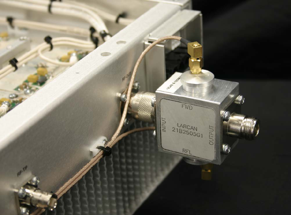
1 MXi401/802U EXTERNAL DIRECTIONAL COUPLER
A dual directional coupler assembly is installed on the final combined output connector of the amplifier. The
assembly consists of a short section of coaxial air line housed within an aluminum block with two adjustable RF
sampling probes installed opposite one another at the midpoint of the line. The N(M) connector on the directional
coupler input connects directly to the amplifier N(F) output connector. Figure 1 is a front view of the directional
coupler.
Figure 1 Front View of External Directional Coupler
Each of the two probes can independently be adjusted to sample either the forward or reflected power on the
main line with a high degree of directivity. The directivity of these probes is a measure of their ability to distinguish
between signals flowing in only one direction on the main line. One of the probes is adjusted to sample the
forward (FWD) RF signal in the main line and the other probe is adjusted to sample the reflected (RFL) RF signal.
Each probe has a single SMA(F) output connector that is used to feed the RF samples back to the metering and
VSWR circuits within the amplifier.
Each probe assembly (11A1871G1) consists of a cylindrical aluminum housing with a circular printed circuit board
(PCB) mounted on one end. An SMA(F) connector is attached to the other end of the housing. Its long centre pin
extends through the housing and is soldered to the small trace on the PCB. The other end of this trace is
terminated by a 50 ohm 1W resistor on the underside of the board. The trace on the circuit board has a nominal
impedance of 50 ohms and so the probe itself exhibits a good match. The probe is installed in the directional
coupler housing so that the trace is parallel to the inner conductor of the coaxial air line. In this manner, the depth
of the probe will determine the level of signal that is coupled from the main line within certain limits. The probe
must be kept far enough away that it does not seriously affect the main line matching, yet not so far away that the
absence of the probe causes the same condition.
MXi401/802U EXTERNAL DIRECTIONAL COUPLER
PUB07-029 Rev 0 July 17, 2007 07-029-2 MXi401/802U External Directional Coupler
These probes (when installed in a matched housing) are specified as having a minimum directivity of 30dB, but
they typically will reach 35dB. Good directivity is most critical when trying to measure the small level of reflected
power on the main line in the presence of the forward signal. In a typical RF system, the reflected level would be
at least 20dB lower than the forward level on the main line. The probe set to measure the reflected power then
needs to reject the forward signal that is at least 100 times greater in power. A probe that is installed with the
output connector towards the system output is sampling the reflected power. However, both forward and reflected
power on the main line is being coupled into that probe. Coupling into the probe is both capacitive and inductive in
nature and gives the probe its directional ability. Ideally, both the capacitive and inductive coupled signals are the
same level, but this is rarely the case. Rotating the probe however does allow some control over the level of the
inductive coupled signal. When the two signals are equal in amplitude, a null occurs since the two signals are
opposite in phase and cancel out at one end of the trace. The null position is determined by measuring the
reverse coupling with a reference quality load on the directional coupler output. The probe is rotated until the null
is reached and then it is locked in place with a set screw. The forward coupling of the probe is then measured and
adjusted if necessary and then the null position is determined again. This process is repeated until the null
position is determined at the required forward coupling level as the forward coupling also changes with the angle
of rotation.
The directional coupler is factory set and should not be adjusted. The angle of probe rotation is dependant on the
probe depth and is set precisely at the null. A typical setup requires a precision measurement system in order
guarantee that the directivity reading is real. If a non-precision setup is used, a null reading can still be attained,
but the directivity reading will be false under those conditions. A reference load with a return loss reading of at
least 40dB (VSWR 1.02) is used at the factory to set the directivity of the probes.
The coupling level of the probes is listed as nominally -40dB±0.5dB, but this is true at the setup frequency of
650MHz only. The coupling varies by about 5dB over the frequency range of 470MHz to 860MHz, with a value of
-42.8±0.5dB at 470MHz to -37.7±0.5dB at 860MHz.
MXi802U POWER SUPPLY CHASSIS
PUB07-014 Rev 0 January 9, 2007 07-014-i MXi802U Power Supply Chassis
CONTENTS
1 MXi802U POWER SUPPLY CHASSIS ..........................................................................................................................1
FIGURES
FIGURE 1 FRONT VIEW OF MXI802U POWER SUPPLY CHASSIS ...................................................................................................1
FIGURE 2 REAR VIEW OF MXI802U POWER SUPPLY CHASSIS .....................................................................................................1
FIGURE 3 MXI802U POWER SUPPLY CHASSIS INTERIOR..............................................................................................................2
FIGURE 4 41D2173 MXI802 POWER SUPPLY CHASSIS WIRING SCHEMATIC SHT1 REV 0.............................................................3
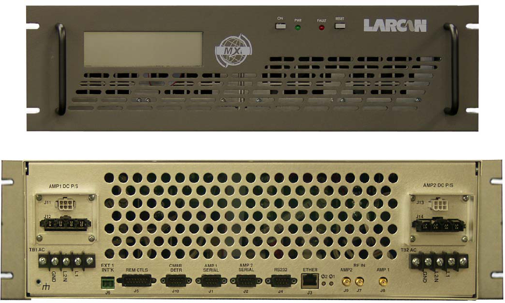
MXi802U POWER SUPPLY CHASSIS
PUB07-014 Rev 0 January 17, 2007 07-014-1 MXi802U Power Supply Chassis
1 MXi802U POWER SUPPLY CHASSIS
The MXi802U Power Supply Chassis Assembly 41D2164G2 consists of a standard 19" rack mountable 5.25"
(3RU) enclosure containing the power supplies, a front panel interface boards, the touch LCD and the main
controller board with connectors for interfacing to external equipment. Figure 1 is a front view of the MXi802U
power supply chassis.
Figure 1 Front View of MXi802U Power Supply Chassis
Figure 2 Rear View of MXi802U Power Supply Chassis
The rear of the MXi8020U Power Supply Chassis has the following connectors:
• 12V and main DC monitoring and control for Amp 1(J11) and Amp 2 (J13)
• Main DC connection to Amp 1 (J12) and Amp 2 (J14)
• AC connections for both power supply 1 (TB1) and power supply 2 (TB2)
• EXT1 INT’K interlock connection (J6)
• REM CTLS remote control 15-pin D-shell connector (J5)
• CMBR DETR combiner metering and AMP1 and AMP 2 on/off control (J10)
• AMP1 SERIAL nine-pin connector (J1)
• AMP2 SERIAL nine-pin connector (J2)
• RS232 serial nine-pin connector (J4)
• ETHER RJ45 Ethernet connector (J3)
• AMP2 RF OUT SMA connector (J9)
• RF IN SMA connector (J7)
• AMP1 RF OUT SMA connector (J8)
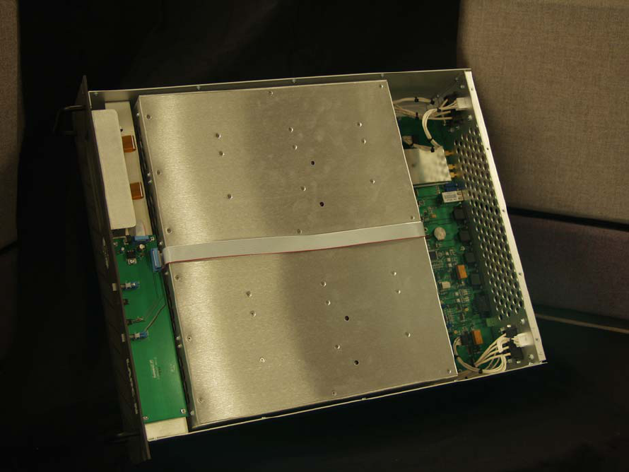
MXi802U POWER SUPPLY CHASSIS
PUB07-014 Rev 0 January 17, 2007 07-014-2 MXi802U Power Supply Chassis
The MXi802U power supply chassis houses two high efficiency 2000W self cooled switching power supplies.
Each power supply provides power to one of the amplifiers, there is no current sharing between power supplies.
The chassis also contains the main user interface and overall system monitoring.
The main controller mounted at the rear of the chassis reads the current consumption of each power supply using
onboard current sensors. It also communicates with each amplifier serially through two serial ports mounted on
the board. Also mounted on the main controller is a 2 way splitter that takes the RF IN from the upconverter and
splits it so it can be sent to each amplifier.
The touch LCD on the front panel provides the user with status and telemetry information from each amplifier as
well as over all metering information from the combined amplifiers. This information is gathered from the main
controller though the serial communications with each amplifier along with the overall telemetry readings from the
2-way combiner.
Figure 3 MXi802U Power Supply Chassis Interior
The chassis is wired according to the functional diagram 41D2173 as shown in Figure 4.
MXi401/802U POWER SUPPLY
PUB07-015 Rev 0 January 9, 2007 07-015-i MXi401/802U Power Supply
CONTENTS
1 MXi401/802U POWER SUPPLY PFC2K-3212A-P6951................................................................................................1
2 POWER SUPPLY DATA SHEET REPRINT ................................................................................................................3
FIGURES
FIGURE 1 MXI401U POWER SUPPLY ............................................................................................................................................1
FIGURE 2 TERMINAL INTERFACES ................................................................................................................................................1
FIGURE 3 POWER SUPPLY OUTLINE DRAWING .............................................................................................................................5
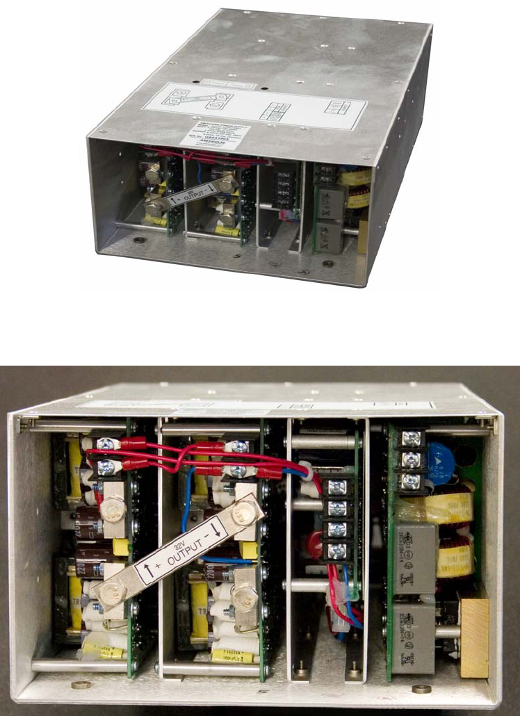
MXi401/802U POWER SUPPLY
PUB07-015 Rev 0 January 09, 2007 07-015-1 MXi401/802U Power Supply
1 MXi401/802U POWER SUPPLY PFC2K-3212A-P6951
The PFC2K-3212A-P6951 power supply used in the MXi401U and MXi802U UHF amplifiers is a free-standing,
power factor corrected 2000W unit. It has the capability to deliver up to 62A when the power supply output is set
to +32VDC. The design of this unit results in a highly efficient power supply ideal for the MXi401U power level.
This unit also contains an internal auxiliary 12VDC power supply rated at 3A which is used to provide power to the
MXi Controller board as well as supplying power to the cooling fans. This auxiliary power supply provides
+12VDC output as long as the main AC input is present.
Figure 1 MXi401/802U Power Supply
There are 2 terminal blocks used for connecting the AC and the Auxiliary voltage and monitoring. The Main DC
power is connected to the large lugs on the right hand side of the power supply.
Figure 2 Terminal Interfaces

MXi401/802U POWER SUPPLY
PUB07-015 Rev 0 January 09, 2007 07-015-2 MXi401/802U Power Supply
TB1 TERMINAL/DESCRIPTION FUNCTION
1. GND AC GND
2. PH AC Phase (Line)
3. N AC Neutral
TB2 TERMINAL/DESCRIPTION
FUNCTION
1. -12VDC OUTPUT (–) return of the 12V power supply
2. +12VDC OUTPUT +12VDC for powering the MXi controller
3. POWER GOOD A High (+12V) is measured here if the +32V power supply is OK
4. +12V ENABLE INPUT If +12V is applied here, it will turn ON the +32VDC power supply.
This enable signal comes from the MXi controller board provided the
interlocks are closed and there are no fault conditions.
32V TERMINAL/DESCRIPTION FUNCTION
1. +32VDC OUTPUT +32VDC output of the power supply
2. -32VDC OUTPUT (–) return of the 32V power supply
MXi802U 2-WAY COMBINER AND REJECT LOAD ASSEMBLY
PUB07-010 Rev 0 January 9, 2007 07-010-i MXi802U 2-Way Combiner and Reject Load Assembly
CONTENTS
1 2-WAY COMBINER AND REJECT LOAD ASSEMBLY 31C1902G1.......................................................................1
2 CIRCUIT DESCRIPTION: COMBINER ASSEMBLY................................................................................................2
3 CIRCUIT DESCRIPTION: REJECT LOAD ASSEMBLY..........................................................................................3
4 CIRCUIT DESCRIPTION: RF AND DC DIRECTIONAL COUPLERS ...................................................................4
5 SPECIFICATIONS ...........................................................................................................................................................5
FIGURES
FIGURE 1 MXI802U 2-WAY COMBINER.......................................................................................................................................1
FIGURE 2 31C1902A1 MXI802 2-WAY COMBINER AND LOAD ASSEMBLY SHT1.........................................................................6
FIGURE 3 21B2544 MXI802 2-WAY COMBINER AND LOAD SCHEMATIC SHT1 ............................................................................7
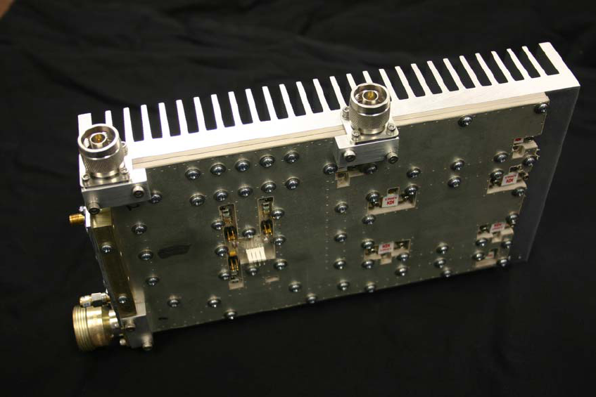
MXi802U 2-WAY COMBINER AND REJECT LOAD ASSEMBLY
PUB07-010 Rev 0 January 9, 2007 07-010-1 MXi802U 2-Way Combiner and Reject Load Assembly
1 2-WAY COMBINER AND REJECT LOAD ASSEMBLY 31C1902G1
A traditional RF power combiner arrangement consists of a 3dB hybrid coupler, a high power termination load,
and various cables to connect the four ports of the coupler to the amplifier and load. The combiner assembly
described here includes the 3dB hybrid coupler and the termination load as well as connectors in a single
package. The two amplifier output signals enter the combiner via ‘N’-type connectors at J1 and J2 and are
combined together by hybrid coupler HY1. The combined output signal passes through two directional couplers
before exiting the assembly at J3, a 716-DIN type RF connector. Isolation between the two amplifiers is provided
by a reject load assembly on the fourth port of HY1. Power entering this port is sampled by a directional coupler
before being directed to a hybrid splitter assembly formed by HY2 through HY4. On two ports of HY3 and HY4 are
RF power terminations to dissipate any imbalance in the amplifiers.
This combiner assembly is intended to mount directly on the RF output connectors of two MXi401 amplifiers with
the combined output port J3 facing upwards. This arrangement aligns the heatsink fins of the combiner assembly
with the air outlet of both amplifiers to provide cooling. Maximum power is dissipated in the reject load portion of
the assembly when one of the amplifier units is shut off. The remaining amplifier unit will provide sufficient cooling
for the power terminations in this situation.
Figure 1 MXi802U 2-Way Combiner
MXi802U 2-WAY COMBINER AND REJECT LOAD ASSEMBLY
PUB07-010 Rev 0 January 9, 2007 07-010-2 MXi802U 2-Way Combiner and Reject Load Assembly
2 CIRCUIT DESCRIPTION: COMBINER ASSEMBLY
RF power from the two MXi401 amplifier assemblies enters the combiner at J1 and J2. In order for proper
combining to take place, these two signals must be the same amplitude and in quadrature phase (ie. 90° phase
difference with J1 lagging J2). The proper phasing is provided by the RF splitter that feeds the two amplifiers. A
similar wide band quadrature hybrid is used to split the RF signal, but each signal also passes through a variable
phase circuit to correct for any errors in the cables feeding the amplifiers.
The hybrid couplers described here are constructed from coupled transmission lines, essentially two lines etched
on either side of a printed circuit board (PCB) directly over top of one another. Transmission lines arranged in this
manner are referred to as ‘Broadside Coupled Lines’. These coupled lines (and all interconnecting lines) are
etched on a ceramic-loaded Teflon-fiber substrate that is 0.020” thick and referred to as the middle board or
coupled section. On either side of this middle board is a 1/8” thick board of the same material with full ground
plane on the outside surface. The entire sandwich is nearly 0.28” thick when all of the copper layers are added in.
A lot of heat is generated by the insertion loss of the 3dB coupler when it is used at such high power. The
ceramic-loaded Teflon-fiber PCB substrate has a rather high thermal conductivity rating and so it is able to
transfer the heat to the heatsink on which the boards are mounted.
Hybrid couplers of this type are fully symmetrical such that any one of the four ports may be chosen as the output
(when used as a combiner) or input (when used as a splitter). The transmission lines that connect the hybrid
couplers to the input and output ports are etched on whatever side of the middle board is most convenient. Strictly
speaking, these transmission lines are called ‘Offset Striplines’ because they are not fully centered between the
ground planes.
When an RF signal within the proper frequency range of the 3dB hybrid coupler is applied to one port of the
coupled lines (assuming all other ports are properly terminated), two signals of equal power (within 1dB) appear
at the two output ports. These two signals will have a 90° phase difference, with the mainline output port lagging
the coupled port. The mainline is considered the line with DC connection between the input and one of the output
ports. The coupled port has no DC connection to the input, but does have a DC connection to the termination
resistor. When looking at the 3dB hybrid as a combiner, each of the input ports may be treated separately and
viewed as a splitter. The resulting signals arriving at the output port add since they are equal in amplitude and
phase while the signals arriving at the reject port cancel because they are opposite in phase.
The following formulas may be used to determine the power level at both the combined output and reject ports of
the coupler
For a single 3dB hybrid coupler: Pout = ½(P1 + P2) + [√(P1P2)] cosθ {1}
Prej = ½(P1 + P2) – [√(P1P2)] cosθ {2}
P1 and P2: power at each input port
Pout: combined output power
Prej: power dissipated in the reject load
Θ: phase error between P1 and P2
Maximum combined output power is achieved when power directed to the reject load is at a minimum. This
occurs when the two input signals have the same amplitude (P1=P2) and the phase error between the two signals
is zero (Θ=0°). Whenever there is a phase error and/or an amplitude difference, then some of the available power
is directed to the reject load. The maximum power level in the reject load occurs when only a single amplifier is
operating into the combiner HY1. The hybrid then acts as a signal splitter, sending half of the input power to
combined output and the other half to the reject load. Referring to formulas {1} and {2}, when either P1=0 or
P2=0, the second term in each expression reduces to zero and the result is Pout=Prej=½P1 or ½P2, depending
on which one is off. When power is directed to the reject port of the hybrid HY1, it is dissipated in power
terminations R17 through R20.
MXi802U 2-WAY COMBINER AND REJECT LOAD ASSEMBLY
PUB07-010 Rev 0 January 9, 2007 07-010-3 MXi802U 2-Way Combiner and Reject Load Assembly
3 CIRCUIT DESCRIPTION: REJECT LOAD ASSEMBLY
The reject load is intended to dissipate any imbalance between the amplifiers in either amplitude and/or phase.
RF power entering the reject load first passes through a directional coupler that provides a DC signal relative in
level to the amount of power being dissipated.
As mentioned in the previous section, the maximum reject load power occurs when one of the amplifiers is off.
The maximum level as calculated is ½ of the remaining input power, or ¼ of the rated combined output power.
With a combiner rating of 1200W sync peak visual (715W average RF maximum) and 120W aural, the reject load
must be rated for at least (715+120)/4 = 209W. The reject load used here is comprised of four power terminations
operating in parallel. Under ideal conditions (termination flange <100°C), each power termination is rated for
250W average RF power, but in many cases the flange temperature exceeds the allowable level and so they are
de-rated.
After the RF power passes through the directional coupler, it is applied to one port of hybrid 3dB coupler HY2
where it is split into two equal level signals. Each of these output signals is split gain by HY3 and HY4 providing a
total of four equal output signals each of which is terminated by a load resistor (R17 through R20). The fourth port
of HY2 through HY4 is also terminated by a low power balancing resistor (R14 through R16). In its simplest form,
the load is essentially a four way splitter with high power terminations attached to each output.
Hybrid couplers HY2 through HY4 are constructed identically to HY1, but in this case are employed strictly as
signal splitters.
MXi802U 2-WAY COMBINER AND REJECT LOAD ASSEMBLY
PUB07-010 Rev 0 January 9, 2007 07-010-4 MXi802U 2-Way Combiner and Reject Load Assembly
4 CIRCUIT DESCRIPTION: RF AND DC DIRECTIONAL COUPLERS
A total of three directional couplers are employed to aid in determining the state of the combiner. A ‘coupler’
directs a small portion of the signal in the main transmission line so that it may be viewed without affecting the
main signal. The ‘directional’ nature of the coupler allows it to determine the direction in which the signal it is
sampling was traveling in the main line, either toward the load (forward) or back from the load (reflected). All three
directional couplers are constructed in a similar way by laying a second transmission line parallel to the main line
and spaced in the vicinity of ¼” away. The distance between the main line and the coupled line will determine the
level of coupled RF signal. The length of the coupled line is made to be about 90° long at 650 MHz so that it
covers the entire UHF band with a variation of ±0.5dB in coupled level.
All of the directional couplers couple a small portion of the RF signal in the mainline onto the parallel coupled line.
In the case of the RF directional coupler, an RF port is attached to each end of the coupled trace. A spectrum
analyzer may be connected to either the ‘Forward’ port J4 or the ‘Reflected’ port J5 to view the signal level flowing
in the two directions. The opposite port must always be terminated by a precision RF termination in order that the
measurement be reasonably accurate. The RF directional coupler has a ‘Directivity’ of at least 30dB when
properly terminated. The directivity of a directional coupler is a measure of its ability to distinguish between
signals flowing in each direction on the main line. It is most critical when trying to measure a low level reflected
signal in the presence of the much higher level forward signal. With a directivity of 30dB, a directional coupler can
measure an actual return loss of 20dB with an accuracy of approximately ±3dB. This means that a difference
reading of 20dB between the forward (J4) and reflected (J5) ports represents an actual return loss of between
23.3dB and 17.6dB. The accuracy changes as a function of both the directivity and the actual return loss.
The other two directional couplers are terminated in 50 ohm resistors (R1, R5, R9, R13) and have diode detector
circuits attached in order to provide a relative DC signal. The directivity of the reflected coupler is limited and is
really only useful in accurately measuring high reflected levels such as those that cause VSWR shutdown. There
are three signals that are being sampled by these two directional couplers. The combined forward power is
sampled and detected by CR1 and directed through smoothing components R2, C1-C3, and L1 before reaching
connector J6-3. The signal level is reduced somewhat by voltage divider resistors R3 and R4. The output
reflected power is detected by CR2 and directed to J6-4 via smoothing components R6, C4-C6, and L2. The
signal level is reduced by an equivalent amount as the forward by R7 and R8 in order to preserve the actual
relationship between the forward and reflected signal levels. Only a forward sample of the signal into the reject
load is detected by CR3. Components R10, C7-C9, and L3 smooth the signal prior to it reaching J6-2. Again, the
DC signal level is attenuated by a voltage divider comprised of R11 and R12. In all cases the voltage divider
output represents 80% of the input level when all outputs from J6 are terminated in 100k ohms (as is the case
when this combiner is used in conjunction with an MXi802 control board).
MXi802U 2-WAY COMBINER AND REJECT LOAD ASSEMBLY
PUB07-010 Rev 0 January 9, 2007 07-010-5 MXi802U 2-Way Combiner and Reject Load Assembly
5 SPECIFICATIONS
Frequency Range: 470-860 MHz
RF Input Connector: N-type (Male)
RF Output Connector: 716-DIN (Female)
RF Input Power: 600W Sync Peak Visual + 10% Aural (forced air cooling)
(each input) 300W Sync Peak Visual + 10% Aural (convection cooling)
350W Average Digital (forced air cooling)
175W Average Digital (convection cooling)
Reject Load: 250W Average RF Power (forced air cooling)
125W Average RF Power (convection cooling)
Dimensions: 2.5 x 7.0 x 12.0 (63mm x 178mm x 305mm) (Width x Depth x Height)
(when oriented with the output connector upwards)
Weight: 8 lbs (3.6 kg)
DC / RF Samples: Forward and Reflected DC sample of the Combined RF signal
Forward or Reflected RF sample of the Combined RF signal
Forward DC sample of the Reject RF signal
MXi802U AMPLIFIER CONTROLLER BOARD REV.2
PUB07-012 Rev. 0 January 10, 2006 07-012-i MXi802U Controller Board Rev.2
CONTENTS
1 INTRODUCTION .....................................................................................................................................................1
2 GENERAL OPERATIONS ......................................................................................................................................2
2.1 CONNECTOR AND SIGNAL DEFINITIONS .......................................................................................................................2
2.1.1 J1 BDM (Background Debug Mode) Connection................................................................................................2
2.1.2 J2 Remote RS232 Connection..............................................................................................................................2
2.1.3 J3 Front Panel LCD and Touchpad.....................................................................................................................2
2.1.4 J4 +32 Volt DC Power Supply.............................................................................................................................2
2.1.5 J5 +32 Volt DC Power Supply Sensing (External)..............................................................................................2
2.1.6 J6 Remote Interface .............................................................................................................................................2
2.1.7 J7 Transmitter Switch Interface...........................................................................................................................3
2.1.8 J8 Fan Interface...................................................................................................................................................3
2.1.9 J9 External Controls............................................................................................................................................3
2.1.10 J10 AGC Control .................................................................................................................................................3
2.1.11 J11 Aural Detector (Optional).............................................................................................................................3
2.1.12 J12 Forward RF Sample......................................................................................................................................3
2.1.13 J13 Reflected RF Sample .....................................................................................................................................3
2.1.14 J14 Front Panel LCD Power ...............................................................................................................................3
2.2 JUMPER OPTIONS..........................................................................................................................................................3
2.2.1 BDM Slide Switch S2 ...........................................................................................................................................3
2.3 RF DETECTOR OPERATION...........................................................................................................................................6
2.4 AGC, VSWR AND CUTBACK OPERATION....................................................................................................................7
2.5 INTERLOCKS .................................................................................................................................................................8
2.5.1 Hard Interlocks....................................................................................................................................................8
2.5.2 Soft Interlocks ......................................................................................................................................................9
2.6 EXTERNAL SIGNALS AND REMOTE CONTROL...............................................................................................................9
2.6.1 External #1 Interlock ...........................................................................................................................................9
2.6.2 Remote Interface (Individual)............................................................................................................................10
2.6.3 Serial Interface ..................................................................................................................................................10
2.6.4 Transmitter Switching Interface.........................................................................................................................10
2.6.5 External DC Power Supply................................................................................................................................10
3 SETUP PROCEDURES..........................................................................................................................................11
3.1 RF DETECTOR ............................................................................................................................................................11
3.1.1 Test Equipment Required...................................................................................................................................11
3.1.2 Jumper Installation............................................................................................................................................11
3.1.3 Verify OpAmp Offsets ........................................................................................................................................12
3.1.4 Verify Output Power Level.................................................................................................................................12
3.2 CUTBACK PROTECTION ..............................................................................................................................................13
3.3 VSWR PROTECTION...................................................................................................................................................13
3.4 POWER SUPPLY VOLTAGE AND CURRENT CALIBRATION ...........................................................................................14
4 REMOTE CONTROL CONNECTIONS MXi TRANSMITTER.......................................................................15
4.1 STATUS OUTPUTS.......................................................................................................................................................15
4.2 TELEMETRY OUTPUTS ................................................................................................................................................15
5 CIRCUIT DESCRIPTIONS...................................................................................................................................17
5.1 MC68HC908 MICROPROCESSOR ...............................................................................................................................17
5.2 POWER SUPPLY VOLTAGE AND CURRENT MONITORING ............................................................................................18
5.3 ON/OFF RELAY K1 ...................................................................................................................................................20
5.4 AGC, CUTBACK AND VSWR ...................................................................................................................................20
5.5 SPI UART..................................................................................................................................................................21
5.6 SPI NVPOT ...............................................................................................................................................................22
5.7 RF DETECTOR ............................................................................................................................................................22
MXi802U AMPLIFIER CONTROLLER BOARD REV.2
PUB07-012 Rev. 0 January 10, 2006 07-012-ii MXi802U Controller Board Rev.2
5.7.1 Circuit Description ............................................................................................................................................22
5.8 J12 CHANNEL – VISUAL FORWARD ............................................................................................................................22
5.9 J13 CHANNEL – REFLECTED.......................................................................................................................................23
5.10 J12 CHANNEL – AURAL FORWARD.............................................................................................................................24
6 ADDENDUMS.........................................................................................................................................................25
6.1 ADDENDUM 1–DUAL DIGITAL POTENTIOMETER WITH EEPROM .............................................................................26
6.2 ADDENDUM 2–SPI/MICROWIRE-COMPATIBLE UART AND +/-15KV ESD-PROTECTED RS-232 TRANSCEIVERS
WITH INTERNAL CAPACITORS.....................................................................................................................................29
6.3 ADDENDUM 3–MC68HC908GTXX DATA SHEET .....................................................................................................32
FIGURES
FIGURE 1 MXI CONTROLLER........................................................................................................................................................1
FIGURE 2 COMB SUBMENU SCREEN............................................................................................................................................7
FIGURE 3 STATUS OUTPUTS........................................................................................................................................................15
FIGURE 4 MXI CONTROLLER BOARD ASSEMBLY DIAGRAM 31C1897A2 SHT1 REV 2.2 ............................................................39
FIGURE 5 MXI CONTROLLER BOARD SCHEMATIC 31C1897S1 SHT1 REV 2.3............................................................................40
FIGURE 6 MXI CONTROLLER BOARD SCHEMATIC 31C1897S2 SHT2 REV 2.3............................................................................41
FIGURE 7 MXI CONTROLLER BOARD SCHEMATIC 31C1897S3 SHT3 REV 2.3............................................................................42
FIGURE 8 MXI CONTROLLER BOARD SCHEMATIC 31C1897S4 SHT4 REV 2.3............................................................................43
FIGURE 9 MXI CONTROLLER BOARD SCHEMATIC 31C1897S5 SHT5 REV 2.3............................................................................44

MXi802U AMPLIFIER CONTROLLER BOARD REV.2
PUB07-012 Rev 0 January 10, 2006 07-012-1 MXi802U Amplifier Controller Board Rev.2
1 INTRODUCTION
This manual describes revision 2.0 or higher of the circuit board.
The MXi amplifier control board (Assembly 31C1897) is a single-circuit assembly that provides all of the amplifier
control functions required for the MXi series of transmitters on a single circuit board. This board can be configured
for a number of different transmitter types, power levels, transmission standards and options.
Figure 1 MXi Controller
The board implements controls/status/telemetries for remote control through a rear panel connector that will
interface to a typical remote control system (such as Moseley or Gentner), when used in a MXi802 the controls
are disabled. An RS232 serial port is also provided to allow the operator to communicate with the MXi802 main
controller located inside the power supply chassis. The MXi control board has RF detectors for forward and
reflected power and all the circuitry to support AGC/VSWR/Cutback functions.
The MXi board has a BDM (Background Debug Mode) connector that allows an external computer or laptop to
download the software program into the CPU chip. The CPU chip holds the program in its internal Flash memory
and so there is no external chip or device that need be replaced to change/upgrade the software.
The concept of this design places all of the control and monitoring functions in one place and therefore eases the
setup and maintenance functions on this series of transmitters.
MXi802U AMPLIFIER CONTROLLER BOARD REV.2
PUB07-012 Rev 0 January 10, 2006 07-012-2 MXi802U Amplifier Controller Board Rev.2
2 GENERAL OPERATIONS
2.1 CONNECTOR AND SIGNAL DEFINITIONS
The connectors on the MXi control board are all shown in Figure 7, which is sheet #3 of the Schematic. The
individual signals that are associated with each pin of the connector are also given. A brief description of each of
the connectors on the board follows.
2.1.1 J1 BDM (Background Debug Mode) Connection
This is used by the software developer to debug the software programmed into the HC08 CPU.
The software program is also downloaded into the HC08 CPU via this connector.
The operator has no real use for this connector since it requires a special interface board.
2.1.2 J2 Remote RS232 Connection
This connector would normally have a nine-pin ribbon cable attached to route the serial signals to the rear panel
nine-pin D-shell connector. Although J2 has 10 pins, only the first nine are actually used with pin 10 being left
open. A typical three-wire serial port (TxD, RxD and Ground) is implemented on this connector to allow interface
to an external laptop or PC. When used in an MXi802 this connection is used to communicate with the main
controller located inside the power supply chassis.
2.1.3 J3 Front Panel LCD and Touchpad
This uses a ten-wire ribbon cable to send and receive serial data from the Front Panel LCD/Touchpad assembly.
This connection is a typical three-wire serial port (TxD, RxD and Ground) that communicates with the
LCD/Touchpad. This connection is not used in an MXi802; the touchscreen is located in the power supply
chassis.
2.1.4 J4 +32 Volt DC Power Supply
This is a two-pin connector used for the +32VDC power that is supplied to the RF amplifier. The +32V source is
fed into one pin, run through a current sensor on the MXi board and then fed back out the second pin to the RF
Amplifier. This is the manner in which the current that the +32V power supply is measured. The voltage telemetry
sample from the +32V power is also taken from this connector. When an internal power supply without its own
current metering is being used, this connector is functional. If an external power supply with its own current
sensing is being utilized, as in an MXi401 or 802, this connector is left open.
2.1.5 J5 +32 Volt DC Power Supply Sensing (External)
This uses a six-pin connector that has all the interface connections for the +32V power supply. Included is an ON
command, P/S OK status and a ground reference from the power supply. In the case of a MXi401 or MXi802
where an external power supply is being used with its own current metering, the +32V sample and the current
telemetry is fed into this connector.
The last signal on this connector is a +12V power supply input (either from the +32V power supply or an external
+12V power supply) that is used to power the MXi amplifier controller board itself. The ground reference is shared
with that of the +32V power supply.
2.1.6 J6 Remote Interface
This uses a 15-wire ribbon cable to send status/telemetry and receive commands from the rear panel 15-pin D-
shell connector. Although J6 has 16 pins, only the first fifteen are actually used with pin 16 being left open. In
addition to the remote signals, there is a single set of contacts made available as an external interlock. This can
connect to an external device or be used as a simple remote ON/OFF. When this board is used in a MXi802 the
controls are disabled but the status and telemetries are still available.
MXi802U AMPLIFIER CONTROLLER BOARD REV.2
PUB07-012 Rev 0 January 10, 2006 07-012-3 MXi802U Amplifier Controller Board Rev.2
2.1.7 J7 Transmitter Switch Interface
This uses a nine-wire ribbon cable to send status/telemetry and receive commands from the rear panel nine-pin
D-shell connector. Although J7 has 10 pins, only the first nine are actually used with pin 10 being left open. This
ribbon cable may not be installed if there is only a single transmitter system or if there is no transmitter switching
unit included in the RF system.
2.1.8 J8 Fan Interface
This uses a special connector mounted on the bottom of the MXi amplifier controller board to connect to the fan
assembly. The fan assembly normally includes up to four fans that are mounted below the MXi amplifier controller
board and is inserted from the bottom of the transmitter control chassis. This connector has ON/POWER control
for each of the fans along with a ground reference and a rotational status signal that comes from each of the fans.
2.1.9 J9 External Controls
This has a seven-pin connector that is used to input a variety of signals into the MXi amplifier controller. A pair of
pins are used for the External interlock that is connected to a terminal block on the rear chassis (this is in parallel
with the external interlock on the Remote Controls J6). There is also a thermal interlock that is sent from the RF
amplifier. Provision has been made for a thermistor input to measure temperatures for testing purposes. A remote
control VOR (Video Operated Relay) input (RC_VOR) is made available which is in parallel with the RC_VOR
control input of the Remote Controls J6.
2.1.10 J10 AGC Control
This is a three-pin connector that sends a DC reference voltage (with ground reference and shield) to the RF
preamplifier module. This DC reference is generated by the AGC circuitry on the MXi amplifier controller to control
the RF output level of the amplifier.
2.1.11 J11 Aural Detector (Optional)
This is an 11-pin connector that allows the option aural RF detector to be mounted above the normal RF
detectors. This connector is located in the shielded box on the left side of the MXi amplifier controller board and is
not normally visible if the cover is installed on the shield box.
2.1.12 J12 Forward RF Sample
This SMA connector receives the forward power sample from the directional coupler built into the 4 way combiner
mounted at the rear of the heatsink. This is used by the RF detector to monitor the level of the RF forward power.
2.1.13 J13 Reflected RF Sample
This SMA connector receives the reflected power sample from the directional coupler built into the 4 way
combiner mounted at the rear of the heatsink. This is used by the RF detector to monitor the level of the RF
reflected power.
2.1.14 J14 Front Panel LCD Power
This is a two-pin connector that sends power (+5V and ground) to the Front Panel LCD/Touchpad assembly if one
is present.
2.2 JUMPER OPTIONS
2.2.1 BDM Slide Switch S2
This two pole switch is used to allow the programming of the microprocessor memory with an external
programmer. It is not normally required by the field personnel unless an upgrade of the internal software is
required. This switch should be in the "NORM" position which is away from the top of the board.
MXi802U AMPLIFIER CONTROLLER BOARD REV.2
PUB07-012 Rev 0 January 10, 2006 07-012-4 MXi802U Amplifier Controller Board Rev.2
2.2.1.1. Dip Switch S3 System Configuration
These DIP switches are reserved for factory test and system configuration. At the time of publication, they are not
assigned for specific functions. When loading the program code into the HC08 micro, these two dip switches
must be in the closed position.
2.2.1.2. Jumper E1–Debug/Normal Mode
This jumper allows factory programming and debug of the HC08 microcontroller. This should always be in the
Normal position for proper operation in the field.
2.2.1.3. Jumper E2–Remote Control Reset
This jumper allows the operator to use the remote Reset command to effect a reset of the HC08 microcontroller.
This would only be installed if there were a suspicion that the microprocessor is hanging-up and the operator
would intend to reset it remotely. This is purely for diagnostic purposes only and should not normally be
permanently installed.
2.2.1.4. Jumper E3–Spare Line Configuration
This jumper allows the signal into the PA0 pin 32 of the HC08 microcontroller to be configured as either an input
or output. This configuration would already have been done in the software at the factory and this jumper setting
should not be altered in the field unless directed by LARCAN personnel.
2.2.1.5. Jumper E4–External or Internal Power Supply Current Sensing
The MXi Amplifier can be configured with a +32VDC power supply that has a built-in current sensing telemetry or,
when the power supply lacks this facility, the MXi controller can measure the current from the +32VDC supply
using the onboard current sensor. When the power supply has its own current sensing telemetry, jumper E4
would be set to the External position. When the power supply does not have its own current sensing telemetry,
jumper E4 would be set to the Internal position allowing the controller’s own current sensor to provide the
telemetry.
The Mxi802 has external power supplies that have their own current sensing and therefore this jumper would be
set in the "Ext" position. This jumper is normally set at the factory and should not be altered in the field.
2.2.1.6. Jumper E5–Front Panel ON/OFF Control Switch (System/Manual)
This jumper controls the function of the front panel ON/OFF switch. When in the Ext position, the ON/OFF
command is fed through the HC08 microcontroller allowing the operator to utilize remote ON and OFF
commands. When in the Int position, the ON/OFF directly controls the ON/OFF relay bypassing the
microcontroller and disabling its OFF control ability.
2.2.1.7. Jumper E6–Tx Switching Interlock Enable
Facility has been designed into the controller interlock chain to allow an external interlock contact that a
transmitter switching unit could use to force the amplifier into an OFF state. This would occur if the controller is
moving a coax switch or if this amplifier has been removed from the antenna. When there is no transmitter
switching unit installed, jumper E6 would be installed to disable this particular interlock.
2.2.1.8. Jumper E7–Manual Remote ON/OFF Control
This jumper would be installed to allow the operator to manually turn the amplifier ON or OFF via a remote
command that would directly control the ON/OFF relay and bypass the HC08 microcontroller. For this mode to
work properly, the front panel ON/OFF switch should be left in the OFF position. In normal operation, this jumper
is not installed.
MXi802U AMPLIFIER CONTROLLER BOARD REV.2
PUB07-012 Rev 0 January 10, 2006 07-012-5 MXi802U Amplifier Controller Board Rev.2
2.2.1.9. Jumper E8–Forward RF Detector, Peak or Average Power
This jumper selects whether the intermediate stage of the RF detector of the Forward power will measure Peak or
Average power. When measuring digital signals, the jumper would normally be set to Average and when
measuring analog signals the jumper would be set to Peak. This jumper determines the amount of RC filtering (or
averaging) of the signal power by selecting which value of resistance is placed in series with capacitor C22. This
jumper is set by the factory depending on the signal standard of the particular amplifier and level that is obtained
from the RF coupler. This should not be changed in the field.
2.2.1.10. Jumper E9–Forward RF Detector Color Burst Trap
When installed, this jumper enables the filter that removes the color burst from the RF signal. This would only be
installed on the analog transmitters, as the digital amplifier does not have a color burst.
2.2.1.11. Jumper E10–Forward RF Detector Sound Carrier Trap
When installed, this jumper enables the filter that removes the sound carrier from the RF signal. This would only
be installed on the analog transmitters, as the digital amplifier does not have a sound carrier.
2.2.1.12. Jumper E11–Forward RF Detector Final Gain Control
This jumper selects either a high or low gain for the final stage of the RF detector of the Forward power. This
jumper is set by the factory depending on the output power of the particular amplifier and level that is obtained
from the RF coupler. This should not be changed in the field.
2.2.1.13. Jumper E12–Reflected RF Detector, Peak or Average Power
This jumper selects whether the intermediate stage of the RF detector of the Reflected power will measure Peak
or Average power. When measuring digital signals, the jumper would normally be set to Average and when
measuring analog signals the jumper would be set to Peak. This jumper determines the amount of RC filtering (or
averaging) of the signal power by selecting which value of resistance is placed in series with capacitor C22. This
jumper is set by the factory depending on the signal standard of the particular amplifier and level that is obtained
from the RF coupler. This should not be changed in the field.
2.2.1.14. Jumper E13–Reflected RF Detector Color Burst Trap
When installed, this jumper enables the filter that removes the color burst from the RF signal. This would only be
installed on the analog transmitters, as the digital amplifier does not have a color burst.
2.2.1.15. Jumper E14–Reflected RF Detector Sound Carrier Trap
When installed, this jumper enables the filter that removes the sound carrier from the RF signal. This would only
be installed on the analog transmitters, as the digital amplifier does not have a sound carrier.
2.2.1.16. Jumper E15–Reflected RF Detector Final Gain Control
This jumper selects either a high or low gain for the final stage of the RF detector of the Reflected power. This
jumper is set by the factory depending on the output power of the particular amplifier and level that is obtained
from the RF coupler. This should not be changed in the field.
2.2.1.17. Jumper E16–AGC Disable Control
When installed, this jumper disables the AGC control of the transmitter and its controller. This is normally only
used with setting up the maximum input drive level for the amplifier. In normal operation, this jumper should
always be removed, since it can allow excessive power to be mistakenly fed through the amplifier.
2.2.1.18. Jumper E17–VSWR Disable Control
When installed, this jumper disables the VSWR trip interlock of the transmitter and its controller. This is normally
only to be used with setting up the VSWR trip level for the amplifier. In normal operation, this jumper should
MXi802U AMPLIFIER CONTROLLER BOARD REV.2
PUB07-012 Rev 0 January 10, 2006 07-012-6 MXi802U Amplifier Controller Board Rev.2
always be removed, since it removes the VSWR protection from the amplifier. In the presence of a VSWR
condition, this could result in damage to the amplifier FET devices.
2.2.1.19. Jumper E18–Manual VSWR Reset Control
When installed, this jumper allows the operator to directly reset the VSWR trip relay and effectively bypass the
HC08 microcontroller. In normal operation, this jumper would not be installed.
2.2.1.20. Jumper E19– Peak or Sync Detection
This jumper allows the forward power sample to be either a Peak detection or Back Porch detection using the
visual sync. The optional Aural detection piggyback board must be installed to provide the sync detection facility.
For most applications (including all of the digital modulation standards), jumper E19 would be set for peak (Pk)
since there is no vertical sync interval that can be locked onto for these signals. The only application where E19 is
set to the Sync position is when the optional Aural Detection board is installed and Back Porch detection for the
Forward power sample is desired. The purpose of using Back Porch detection is to regulate the output power
more precisely, independent of APL level. This jumper is set by the factory and should not be changed in the field.
2.3 RF DETECTOR OPERATION
The RF Detector circuitry is show in Figure 8. This circuitry can be used for internally diplexed analog transmitters
or for digital transmitters.
RF Power levels are sampled by a directional coupler located on the RF amplifier heatsink and the resulting RF
samples are detected and appropriately processed to provide DC outputs corresponding to the amplitude of the
desired parameter of the input signal. These DC outputs contribute to the AGC/VSWR supervision of the
transmitter and are also processed in analog to digital conversion circuits on the MXi amplifier controller board to
provide digital metering.
The RF Detector can have different group assemblies to support the NTSC system, the PAL system and Digital
transmission. NTSC and PAL application differ only in their color subcarrier frequency, consequently in a few
component values. All group assemblies use the same PC Board and have many jumpers used to change circuit
sensitivity, introduce/remove traps for color subcarrier and/or aural intercarrier and change envelope detector
characteristics for digital and analog applications.
The schematic included in this publication shows the circuitry for NTSC and Digital transmissions. For PAL
systems a separate schematic would be included that is currently not in this publication.
All jumpers are set in the factory and should not be modified in the field unless under direction from LARCAN
personnel.
An optional circuit board is available for internally diplexed analog systems to monitor the aural power separated
from the combined forward signal. This board is mounted on top of the existing RF detector circuitry in a piggy-
back configuration. This extra board uses a sync detector to obtain the back porch (blanking level) of the RF
signal and subtracts the overall RF signal level from the visual only signal level to obtain the aural output. When
this extra board is installed, an added benefit is the provision of a more stable visual output level that is more
independent of APL level due to the fact that the blanking level is used to determine power instead of a simple
envelope detection method. Note that the standard MXi transmitter does not come with this extra board installed
but it must be ordered as an option. When the option is included, an addendum to this manual will be included to
cover this option.
Required signal levels are as follows:
• FWD (overall forward sample) metering requires 20dBm sync peak signal for full scale (100% rated power).
• RFL (overall reflected sample) metering requires 10dBm sync peak signal for full scale (10% rated power).
The forward RF detector can be configured for a number of different signal types as the following table shows.
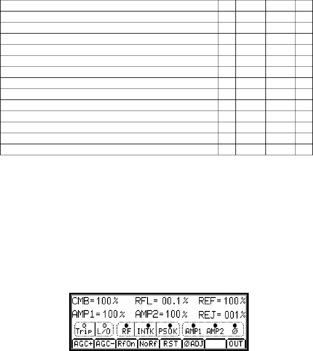
MXi802U AMPLIFIER CONTROLLER BOARD REV.2
PUB07-012 Rev 0 January 10, 2006 07-012-7 MXi802U Amplifier Controller Board Rev.2
DESCRIPTION E8 E9 E10 E11
Default Analog NTSC: +20dBm, Visual, Color Burst and Aur Carrier Trapped Pk Installed Installed LO
Default Analog NTSC: +20dBm, Visual, Color Burst and Aur Carrier Trapped Pk Installed Installed LO
Default Analog NTSC: +17dBm, Visual, Color Burst and Aur Carrier Trapped Pk Installed Installed HI
Default Analog NTSC: +17dBm, Visual, Color Burst and Aur Carrier Trapped Pk Installed Installed HI
Special Analog NTSC: +20dBm, Visual+Aural, Color Burst Trapped Pk Installed Absent LO
Special Analog NTSC: +20dBm, Visual+Aural, Color Burst Trapped Pk Installed Absent LO
Special Analog NTSC: +17dBm, Visual+Aural, Color Burst Trapped Pk Installed Absent HI
Special Analog NTSC: +17dBm, Visual+Aural, Color Burst Trapped Pk Installed Absent HI
Digital Signal: +20dBm, Ave Detector, No Traps (also Special Analog NTSC) Av Absent Absent LO
Digital Signal: +20dBm, Ave Detector, No Traps (also Special Analog NTSC) Av Absent Absent LO
Digital Signal: +17dBm, Ave Detector, No Traps (also Special Analog NTSC) Av Absent Absent HI
Digital Signal: +17dBm, Ave Detector, No Traps (also Special Analog NTSC) Av Absent Absent HI
Not Used: Visual + Color Burst and Aur Carrier Trapped X Absent Installed X
Two almost identical detector circuits reside on a single board for visual forward and reflected metering. Detection
sensitivity of the circuit dedicated to reflected visual power is approximately 10dB greater than for the visual
forward RF detector circuit. The reflected port reading is combined visual and aural power. The jumper
configuration for the reflected power follows that of the above table with E12 replacing E8; E13 replacing E9; E14
replacing E10; and E15 replacing E11.
2.4 AGC, VSWR AND CUTBACK OPERATION
The MXi amplifier control board allows for an automatic gain control to maintain the transmitter’s power at a
predefined level. The operator must have first calibrated the RF detector to produce 4.0VDC at the desired 100%
power level of the transmitter. The exciter/modulator must then be set up to produce a drive level sufficient to
allow 110% power with no AGC controls applied. These operations are described in Section 3.
The AGC system generates a desired reference voltage that is set by the operator through the LCD touchpad on
the main 802 Control Chassis (external to this chassis). To set the AGC, the operator calls up the Comb submenu
from the Main LCD menu. He would then either press the AGC+ button to increase the power level or the AGC–
button to decrease the power level. This sets the reference voltage for the AGC circuitry. If there is very low RF
power, check that the RF status on the third line is lit. If it is not, then the operator has shut down the RF. Pressing
the RF ON menu button restores RF power. The Amps submenu screen is shown below.
Figure 2 COMB Submenu Screen
The AGC circuit then compares this reference voltage to the actual voltage that is produced from the forward
power RF detector. If there is a difference, this is amplified by a high gain OpAmp and this error voltage is fed out
to connector J10. An external cable connects J10 to the attenuator on the RF preamp mounted on the heatsink.
This will lower the drive to the amplifiers until the transmitter power level agrees with the AGC reference voltage.
MXi802U AMPLIFIER CONTROLLER BOARD REV.2
PUB07-012 Rev 0 January 10, 2006 07-012-8 MXi802U Amplifier Controller Board Rev.2
Note the AGC voltage from the LCD, if it is near to a value of 0 (i.e., under 0.1V), then there is no AGC action left
and the power cannot be raised any further. If the amplifier power is under 100%, then check the RFL power level
and CUTBACK voltage to verify that the amplifier is not reducing power to protect from a VSWR condition.
The cutback circuit checks the level of reflected power as displayed on the LCD screen above [RFL=00.1%]. If
this reflected power is greater than 1%, the cutback circuit automatically reduces the amplifier forward power to
protect the devices. This indicates a mild VSWR condition such as may be caused by an icy antenna. The
cutback function is a safety protection and is therefore permanently in circuit and cannot (or should not) be
disabled. If the VSWR condition worsens such that reflected power exceeds 10% of forward power, the MXi shuts
the transmitter down.
The MXi has built-in VSWR protection to prevent damage to the amplifier from excessive power being reflected
back from the output system. This VSWR protection becomes operational when reflected power exceeds 10% of
forward power. The system shuts down the amplifier for a few seconds and then tries to restart again. This is
done to check if the VSWR was a temporary condition that could have been caused by a lightning strike nearby.
The LCD shows the TRIP status light on the third row of the LCD to indicate that a VSWR trip had occurred. If the
condition persists such that three VSWR trips occur within 1 minute, the system completely shuts down. The LCD
will then illuminate the L/O (Lockout) status light on the LCD to show that a Lockout has occurred.
2.5 INTERLOCKS
Interlocks on the MXi amplifier can be divided into two different types: hard interlocks that shut down the amplifier
without any CPU intervention and soft interlocks that are generated by the CPU chip in response to abnormal
system parameters.
2.5.1 Hard Interlocks
There are hardware interlocks that directly affect the ON/OFF relay K1 by removing the +12V arming voltage on
its coil and preventing it from turning on. There are four of these interlocks as follows:
2.5.1.1. Amplifier Thermal
Heatsink thermal opens if heatsink temperature is too high. Dry Contact across Connector J9 pins 5 and 6.
2.5.1.2. Transmitter Switching
Interlock provided for an external Transmitter Switching unit to shut down the Transmitter.
Dry Contact across Connector J7 pins 1 and 2.
When there is no transmitter switching, jumper E6 defeats this interlock.
2.5.1.3. External #1
Interlock supplied for customer use such as RF system interlock or RF Load.
Dry Contact across Connector J9 pins 1 and 2.
Parallel contact provided across J6 pins 14 and 15, only one of J6 or J9 is required.
If not used, then this contact should be shorted out externally.
2.5.1.4. VSWR Relay K2
Contact from VSWR Trip relay K2 pins 11 and 13.
Contact will be closed (OK) if there is no VSWR condition.
Contact will open whenever a VSWR is detected.
Note: Jumper E17 disables this interlock, this is for setup only.
MXi802U AMPLIFIER CONTROLLER BOARD REV.2
PUB07-012 Rev 0 January 10, 2006 07-012-9 MXi802U Amplifier Controller Board Rev.2
2.5.2 Soft Interlocks
There are parameters that the CPU monitors and if they indicate an error condition, the CPU will issue and OFF
command to the ON/OFF relay and set the appropriate error flag. Note: if the Local or Remote ON/OFF
commands are jumpered to the Override state, the CPU will be unable to shut off the amplifier via K2.
For this reason it is recommended that the ON/OFF controls are left jumpered in the normal positions unless an
emergency condition exists. The software interlock parameters are as follows:
2.5.2.1. Power Supply OK
+32V Power Supply is indicating an error, +12V signal at J5 pin 5 means OK state.
2.5.2.2. Power Supply Voltage
+32V telemetry shows a voltage over +34VDC, Telemetry at J5 pin 6.
2.5.2.3. Power Supply Current
Power Supply Current exceeding the max rating, value depends on MXi model.
For the internal power supply, the telemetry is found at U7 pin 7.
For an external power supply, the telemetry if found at J5 pin 5.
2.5.2.4. Amp Temperature
If the amplifier heatsink is configured with a thermistor. This is optional.
When the heatsink temperature rises too high, the CPU cuts back output power.
This is not a true interlock since the Thermal interlock is used to shut off the transmitter.
This power cutback tries to keep the heatsink from reaching shutoff temperature.
2.5.2.5. Fan Failure
The four fans are monitored for their rotational status.
When one or more fans show a failure, the CPU cuts back output power.
This is not a true interlock, as the Thermal interlock is used to shut off the transmitter.
This power cutback tries to keep the heatsink from reaching shutoff temperature.
2.6 EXTERNAL SIGNALS AND REMOTE CONTROL
There are a number of signals that are connected externally at the back panel of the MXi transmitter chassis.
These can be classified as either interlocks, remote controls, external power supplies or transmitter switching.
2.6.1 External #1 Interlock
The interlock that is available on the rear panel is the External #1. This is a single dry contact that is provided to
shut down the RF amplifier in the case of some external problems (such as a bad RF load). It has two possible
connection points that are logically in parallel so that only one needs to be connected. One point is from pins 1
and 2 of J9 on the MXi board. This connector is normally wired to a two-pin terminal block TB1 located on the
back panel. This would be the most accessible and likely connection point.
The second parallel connection is from pins 14 and 15 of J6 on the MXi board which is assigned for Remote
Controls. This 16-pin connector would usually have a 15-wire ribbon cable attached that would route the signals
from the first 15 pins of J6 to a 15-pin D-shell connector on the rear panel.
MXi802U AMPLIFIER CONTROLLER BOARD REV.2
PUB07-012 Rev 0 January 10, 2006 07-012-10 MXi802U Amplifier Controller Board Rev.2
2.6.2 Remote Interface (Individual)
Connector J6 provides for individual lines of control/status/telemetry that would normally be connected to an
external vendor remote control system (such as Moseley or Gentner). This 16-pin connector would usually have a
15-wire ribbon cable attached that would route the signals from the first 15 pins of J6 to a 15-pin D-shell
connector on the rear panel. The details of the signals on this connector are given in Section 4. For on MXi802
the controls are disabled but the status and telemetries are still active.
2.6.3 Serial Interface
Connector J2 provides a standard three-wire serial interface (TxD, RxD and Ground) that is used for
communicating with the main TX controller located in the power supply chassis. The user could also use this port
to connect to an external computer or laptop serial port. The MXi sends a serial stream out this serial port that
reports all of the operating parameters of the transmitter. It can also receive serial commands from an appropriate
computer program or the main TX controller.
2.6.4 Transmitter Switching Interface
Connector J7 provides for individual lines of control/status/telemetry that would normally be connected to an
external transmitter switching unit. Of course, this switching unit would only be necessary if there are two (or
more) MXi transmitters in the system. For a single transmitter, these signals would not be used. When configured
for transmitter switching, this 10-pin connector would usually have a nine-wire ribbon cable attached that would
route the signals from the first nine pins of J7 to a nine-pin D-shell connector on the rear panel. The transmitter
switch interface consists of a telemetry output of the RF forward power level, a status output indicating TX failure,
and interlock input used to shut down the transmitter and a few spare signals for future use. The exact use and
operation of the transmitter switching unit would be documented in its own publication when implemented.
2.6.5 External DC Power Supply
Higher power MXi transmitters such as the Mxi802 require that the DC power supply for the amplifier be located
external to the amplifier chassis. Connector J5 receives the interface signals for this external supply. These
include a +12V input that provides power to the MXi control board itself, a reference ground, a sample of the
+32VDC that is used to power the amplifier, and current telemetry sample and a control output from the MXi
board used to turn on the supply.
The actual connection is made via a power connector at the rear panel and is wired to connector J5. The actual
connection that supplies the amplifier(s) is wired directly from the rear panel to the amplifier and not through the
MXi control board.
MXi802U AMPLIFIER CONTROLLER BOARD REV.2
PUB07-012 Rev 0 January 10, 2006 07-012-11 MXi802U Amplifier Controller Board Rev.2
3 SETUP PROCEDURES
The following sections detail the various set up procedures for the MXi transmitter system. These procedures
should only be done by qualified personnel. If the calibrations and setups are done improperly, it can result in the
transmitter being prone to damage.
The transmitter is normally set up in the factory for the particular operating power required when first installed. Set
up procedures would only be required if certain elements of the MXi transmitter had to be replaced or repaired
that would have affected the calibrations. An example of this would be the MXi amplifier controller board itself, the
output RF couplers, the RF cables or the 32V power supply.
If the output power is being changed, then some setup and calibration would be needed since the transmitter
would be set up for the previous RF power level. Caution: do not increase the power output of the MXi transmitter
beyond the original factory set level without first consulting LARCAN field service.
3.1 RF DETECTOR
The RF detector is normally calibrated at the factory or by LARCAN field personnel and should not require onsite
re-adjustments except in the following circumstances.
• The desired output power level of the transmitter is to be changed from the factory setting for a full 100%
power reading. Note that the operator should not just increase and readjust power beyond the
recommended rating of the transmitter without prior approval from LARCAN technical services.
• A replacement MXi amplifier control board or directional coupler has been installed in the transmitter.
This procedure assumes that the RF detector is being set-up with the transmitter connected to an RF modulator
input and output load (or antenna) that is the actual configuration it is intended to operate with.
3.1.1 Test Equipment Required
a) An RF power meter such as the HP 436A or similar. For analog transmitters, a BIRD through-line
wattmeter is sufficient.
b) A Spectrum Analyzer, HP 8558B or similar.
If the operator wishes to set up the unit on the bench, then a number of extra pieces of test equipment are
necessary.
• An RF generator/modulator that will replicate the desired signal and level
• An analog transmitter would need a video generator such as Tektronix 1900 or similar
• A modulator such as LARCAN TTC (Catel X - ATM -1600 - 6 - 01/01) or similar.
• An upconverter such as Philips PM 5690 or similar (or one supplied with transmitter)
• A digital transmitter would need the Zenith modulator used with the transmitter. With serial data
input, the Zenith will still generate the appropriate digital spectrum
• An upconverter such as Philips PM 5690 or similar (or one supplied with transmitter)
• RF Load rated at the transmitter power and associated cable
3.1.2 Jumper Installation
If the transmitter is not being upgraded from Analog to Digital service (or vice versa), then there should be no
need to change the jumpers for the traps or gain. If there is a change, the trap jumpers would need to be modified
and perhaps the gain as well.
For Analog service, the color burst and aural carrier traps should normally be installed.
For the forward power sample, this would be jumpers E9 and E10.
For the reflected power sample, this would be jumpers E13 and E14.
MXi802U AMPLIFIER CONTROLLER BOARD REV.2
PUB07-012 Rev 0 January 10, 2006 07-012-12 MXi802U Amplifier Controller Board Rev.2
For Digital service, the above four jumpers would not be installed.
If the desired transmitter output power is the same as what the transmitter was originally set up for at the factory,
there should be no need to change the gain jumpers on the RF detectors.
If a change in power is required or the directional coupler has been changed or the transmitter is being moved
between Analog/Digital service, the RF detector should be first set to the lowest possible gain and the jumpers
moved to increase the gain.
For the forward power sample, the gain is controlled by jumpers E8 and E11.
Digital + Low Gain: E8= Av and E11=LO
Digital + High Gain: E8= Av and E11=HI
Analog + Low Gain: E8= Pk and E11=LO
Analog + High Gain: E8= Pk and E11=HI
For the reflected power sample, the gain works identically where E12 is the same as E8 and E15 is the same as
E11.
3.1.3 Verify OpAmp Offsets
1. With no RF signal applied, measure the voltage at TP1 and adjust R58 to make this level under 0.1VDC
2. With no RF signal applied, measure the voltage at TP4 and adjust R80 to make this level under 0.1VDC
3.1.4 Verify Output Power Level
1. Attach the RF output power measuring device (Wattmeter or Average Power Meter) to the RF output.
2. Turn down the drive level of the modulator/upconverter before applying the RF input signal.
3. Turn up the drive level until the output power measures the desired reading. Do not use the meter of the
transmitter itself to determine output power, since at this point it may be uncalibrated.
4. When increasing the power, it is always instructive to measure the current on the 32VDC supply in case
there is a problem with how the output power meter is connected or working. If the supply current is
increasing but the output power is not, set the drive to a sufficiently lower level and double check your
setup.
5. When the RF output power is at the desired level, do the following checks:
a) For the forward power sample, the voltage at TP1 should be within 4.5 to 9.0VDC as a maximum
b) If not, then you have either too much power or too high a coupling in the directional coupler.
6. Reverify the output power: if this is correct, a pad can be inserted between the coupler and J12.
7. Adjust potentiometer R48 until the voltage at TP3 is 4.0VDC.
8. To calibrate the reflected power, install jumper E17 that prevents any VSWR trips
9. Remove the RF cable from J12 and attach a –10dB pad, then connect this reduced forward power
sample to J13.
10. If the original power sample into J12 required a pad, this must be retained in addition to the –10dB pad.
11. For the reflected power sample, the voltage at TP4 should be within 4.5 to 9.0VDC as a maximum
12. If not, reverify that the output power has not changed in the meantime.
13. Adjust potentiometer R80 until the voltage at TP5 is 4.0VDC.
Note: Make sure that you remove jumper E17 when done, else you will have no VSWR protection!
At this point, the operator should proceed to verify cutback and VSWR trip functions, as described in the next two
sections.
MXi802U AMPLIFIER CONTROLLER BOARD REV.2
PUB07-012 Rev 0 January 10, 2006 07-012-13 MXi802U Amplifier Controller Board Rev.2
3.2 CUTBACK PROTECTION
Before the operator attempts to set up the cutback circuitry, the forward and reflected power levels must be
properly set up to calibrated levels as described in Section 3.1.
To set up the cutback level, a power sample must be fed into the reflected power connector of the MXi board that
is –16dB down from the forward power sample level. The most convenient way to accomplish this is to take this
sample from the RF monitor port on the rear of the transmitter chassis.
1. Disconnect the AGC control connector J10 from the MXi board to remove any possible AGC or cutback
action while verifying the Reflected power. If the forward power is greater than 100%, adjust the output
level of the upconverter until it is at 100% (+/- 2%).
2. Attach an RF cable from the RF monitor connector at the rear of the MXi control chassis and insert a
–16dB pad. This pad can consist of a –10dB and –6dB pad in series. Remove the RF cable from J13 that
comes from the output coupler and attach a cable from the –16dB pad off the forward monitor sample.
3. We are assuming that the coupling level from the monitor connector is the same as the coupling level for
the forward power RF coupler. To verify this by checking the RFL power level on the LCD, it should read
around 2.5% power. If it is off by more than 0.5%, adjust the amount of padding until the RFL power
reading is within the range of 2% - 3%. A variable attenuator pad would be ideal for this application.
4. Readjust the upconverter output level so that the forward power reads 110% again.
5. Also disconnect the cable from the monitor port for now.
6. Reconnect the AGC control connector J10 on the MXi board.
7. Reconnect the cable from the monitor port to the reflected power sample at J13.
8. Adjust the potentiometer R105 until the forward power reading is about 96% - 98%, which puts the
system just at the edge of cutback.
The setup is now complete, remove the monitor cable from J13 and attach the output coupler back to J13.
3.3 VSWR PROTECTION
The VSWR protection does not really need any setup or calibration since it is fixed to trip when the reflected
power is –10dB of the forward power level. To verify the VSWR trip function, the following steps must be taken.
To check the VSWR trips, a power sample must be fed into the reflected power connector of the MXi board that is
–10dB down from the forward power sample level. The most convenient way to accomplish this is to take this
sample from the RF monitor port on the rear of the transmitter chassis.
1. Disconnect the AGC control connector J10 from the MXi board to remove any possible AGC or cutback
action while verifying the Reflected power. If the forward power is greater than 100%, adjust the output level
of the upconverter until it is at 100% (+/- 2%).
2. Install a jumper in E17 that will prevent any VSWR trips.
3. Attach an RF cable from the RF monitor connector at the rear of the MXi control chassis and insert a
–10dB pad. Remove the RF cable from J13 that comes from the output coupler and attach a cable from
the –16dB pad off the forward monitor sample. We are assuming that the coupling level from the monitor
connector is the same as the coupling level for the forward power RF coupler. To verify this by checking
the RFL power level on the LCD, it should read over 10.1% power but less than 11% power. Note that a
minimum of 10.1% power is needed to insure a VSWR trip. If the RFL power is under 10.1%, decrease
the amount of padding until the RFL power reading is within the range. If the RFL power is too high (over
11%), increase the amount of padding until it is in the range. A variable attenuator pad would be ideal for
this application.
4. Readjust the upconverter output level so that the forward power reads 110% again.
5. Also disconnect the cable from the monitor port for now.
6. Reconnect the AGC control connector J10 on the MXi board.
MXi802U AMPLIFIER CONTROLLER BOARD REV.2
PUB07-012 Rev 0 January 10, 2006 07-012-14 MXi802U Amplifier Controller Board Rev.2
7. Reconnect the cable from the monitor port to the reflected power sample at J13.
8. Remove the jumper from E17 and the transmitter should trip three times and lock out on the fourth trip.
9. The setup is now complete: remove the monitor cable from J13 and attach the output coupler back to
J13.
10. Clear the VSWR lockout and trip condition by either pressing the front panel reset button or issuing a
remote reset command.
3.4 POWER SUPPLY VOLTAGE AND CURRENT CALIBRATION
The power supply voltage and current readings must be set for both amplifiers. To set up the power supply
voltage and current reading, the operator must view the readings on the Main controller LCD in the power supply
chassis. The values for power supply voltage and current are show for bot amplifiers on the P/S submenu.
Also note that the main controller has its' own individual power supply voltage and current set-up that is distinct
from that of each amplifier. The procedure for doing this is described in the publication for the Main Mxi Control
Chassis and will not be discussed in this publication.
1. To set up the voltage reading, turn on the transmitter and verify that the power supply is indeed running.
2. With a voltmeter, measure the voltage at TB1 (or TB2 if setting up Amplifier 2 readings) on the Main
controller board, 31C1936, located in the power supply chassis.
3. Adjust potentiometer R14 on the MXi amplifier control board until the displayed voltage equals that being
measure by the voltmeter.
4. To set up the current reading, the power supply should be ON as in the above paragraph and enough RF
drive (at least 50%) should be applied to get a reasonable current level for calibration.
5. With a clamp on Ampmeter, measure the current for the pair of wires that pass through the current sensor
of 31C1936, located in the power supply chassis. Current sensor U19 is associated with Amplifier #1 and
Current Sensor U16 is associated with Amplifier #2.
6. On the Mxi amplifier control board, insure that jumper E4 is in the 'Ext' position. Adjust potentiometer R15
until the displayed current agrees with that measured on the clamp on meter.
If an external power supply is used that has its own current telemetry sensing, it may have its own setup as well.
The current reading on the LCD will still be affected by R15 but the external supply may require its own
calibration, if the level it sends to the MXi is too low or high. A good level would be in the range of 2-4 volts for full
scale current.
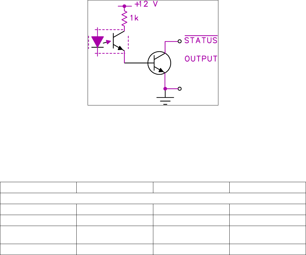
MXi802U AMPLIFIER CONTROLLER BOARD REV.2
PUB07-012 Rev 0 January 10, 2006 07-012-15 MXi802U Amplifier Controller Board Rev.2
4 REMOTE CONTROL CONNECTIONS MXi TRANSMITTER
On the rear of the transmitter Chassis, the remote control connections are available on a 15-pin male D-shell
connector J6. This includes all of the remote controls, status and telemetries available to the operator.
These remote signals are routed from the MXi Control board via a 15-wire ribbon cable from connector J6 of the
MXi Control board. The signals designations for each pin of J6 can be viewed on sheet 3 of the schematic in
Figure 7. The actual circuitry that drives these signals is spread out on all five sheets of the schematic.
When the MXi amplifier controller is used in a MXi802 the remote controls are disabled but the telemetries and
status are still present.
4.1 STATUS OUTPUTS
Figure 3 Status Outputs
These are current sinking open collector outputs, out of quad pack MPQ2222 (2N2222A) NPN transistors driven
by opto-isolator devices. The available output sink current is dependent on the gain of the NPN and the opto-
isolator transfer ratio. Generally, one can expect at least 100mA of sinking current for each output listed here.
Because these are open collector, they can be used in special applications, such as on-site warning signal
activation if desired, but they are limited in external circuit voltage to maximum 60VDC. Each status (in
parentheses) indicates what it means when in its active low condition.
The MXi provides three remote control outputs that represent the current operating state of the switching system
via the Digital Output Board
TX D-Connector PC Board Connector Designation Description
Remote Control
Pin 9 J6 Pin 2 RS TXOn Transmitter is turned ON
Pin 2 J6 Pin 3 RS_Error Transmitter has an error
Pin 10 J6 Pin 4 RS_Remote Transmitter is in Remote
Mode
Pin 12 J6 Pin 8 Ground Ground Reference
4.2 TELEMETRY OUTPUTS
These are buffered OpAmp outputs, out of quad pack LM324 operational amplifiers. The available output voltage
is limited to the range of 0 – 5VDC. The OpAmp can reliably source around 5mA of current and so a relatively
high impedance input of at least 2K ohms should be used. Each telemetry has a description to indicate what
parameter it is measuring.
The MXi provides five remote telemetry outputs that represent the current operating levels of the MXi transmitter.

MXi802U AMPLIFIER CONTROLLER BOARD REV.2
PUB07-012 Rev 0 January 10, 2006 07-012-16 MXi802U Amplifier Controller Board Rev.2
TX D-Connector PC Board Connector Designation Description
Remote Controls
Pin 5 J6 Pin 9 RT_FWD Forward RF power level
Pin 13 J6 Pin 10 RT_RFL Reflected RF power level
Pin 6 J6 Pin 11 RT_AUR Aural RF power level
(optional)
Pin 15 J6 Pin 12 RT_AGC AGC voltage (1/2 scale)
Pin 7 J6 Pin 13 RT_CUTB Cutback voltage (1/2
scale)
Pin 12 J6 Pin 8 Ground Ground Reference
MXi802U AMPLIFIER CONTROLLER BOARD REV.2
PUB07-012 Rev 0 January 10, 2006 07-012-17 MXi802U Amplifier Controller Board Rev.2
5 CIRCUIT DESCRIPTIONS
5.1 MC68HC908 MICROPROCESSOR
The Motorola MC68HC908GT microprocessor (often referred to as the CPU or HC08) performs all of the control
interface and communications in the MXi transmitter system. It is a 44-pin surface mount PLCC type device that is
permanently soldered to the circuit board and is not field serviceable or easily replaced without special surface
mount tooling. A brief description of the part is given in this section and a portion of the manufacturer’s
documentation is given in Appendix A. More detailed information on this part can be obtained from the Motorola
web site.
The HC08 chip used in the MXi can come with either 8K or 16K bytes of non-volatile flash memory, which can be
erased and reprogrammed to allow updating of software code or system parameters. The MXi code is typically
smaller than 8k and so would fit in either size of Flash memory. The HC08 chip has a dedicated serial input pin
designated as the BDM (Background Debug Mode) port that is used to program the internal Flash memory and
for debug testing. The MXi is programmed at the factory and it is not expected that reprogramming would need be
done in the field, although it is possible to do with the proper software. System parameters and status that need to
be retained during power failures (such as the LOG entries) are also stored in the Flash memory.
Most of the external pins on the HC08 are configured as programmable Input/Output (I/O) ports, where the
software program determines whether a certain pin is to be configured as either an input or output. The pins on
the HC08 are grouped together in sets called PORTs. These Ports will have eight pins (or fewer) to support the
byte wide data path in the CPU. Port A is used for general system inputs and outputs. Port B is used as an eight-
channel A/D converter to measure system telemetry values. Port C is used for general system inputs and outputs.
Port D assigns four pins for the synchronous serial port (SPI) with the other four pins used for system inputs. Port
E assigns two pins as a serial communications port (SCI), one pin is the external CPU clock and the other two
pins used for general system inputs and outputs.
The definition of each Port pin is as follows:
PORT A
PA0 Input or Output Jumper E3 configures as I/P or O/P
PA1 Input Remote Control ON Command
PA2 Input Remote Control OFF Command
PA3 Output Select enable for Serial NvPot U16
PA4 Input Front Panel ON Command
PA5 Input Front Panel VSWR RESET Command
PA6 Input 32V Power Supply OK Status
PA7 Input Remote Control VOR Status
PORT B
PB0 Telemetry Temperature of Heatsink [Optional]
PB1 Telemetry Power Supply Current
PB2 Telemetry Power Supply Volts
PB3 Telemetry Cutback Volts [Scaled at half the actual value]
PB4 Telemetry AGC Volts [Scaled at half the actual value]
PB5 Telemetry RF Aural Power [from RF detector - Optional]
PB6 Telemetry RF Reflected Power [from RF detector]
PB7 Telemetry RF Forward Power [from RF detector]
MXi802U AMPLIFIER CONTROLLER BOARD REV.2
PUB07-012 Rev 0 January 10, 2006 07-012-18 MXi802U Amplifier Controller Board Rev.2
PORT C
PC0 Output Remote Status – Error
PC1 Input DipSw #1
PC2 Input Power Supply (Relay K1) ON Status
PC3 Input DipSw #2
PC4 Input External #1 Interlock
PC5 Output VSWR Reset Control
PC6 Output PS ON Ctl +12V out [could be 24V too]
PORT D
PD0 SPI SS Used by UART
PD1 SPI MISO Used by UART and NvPot
PD2 SPI MOSI Used by UART and NvPot
PD3 SPI SCLK Used by UART and NvPot
PD4 Input Fan#1 Status, Active Low
PD5 Input Fan#2 Status, Active Low
PD6 Input Fan#3 Status, Active Low
PD7 Input Fan#4 Status, Active Low
PORT E
PE0 SCI Transmit Data Used by LCD
PE1 SCI Receive Data Used by LCD
PE2 O/P Remote Status – Remote Mode
PE3 Input VSWR Trip Status
PE4 System Main CPU Clock – 4.9152MHz
The HC08 provides two separate serial interfaces to external components, these are the synchronous peripheral
interface (SPI) and the serial communications interface (SCI).
The SCI implements the standard three-wire serial port (Rx Data, Tx Data and Ground) that would interface to a
typical computer port. The baud is set at 9600. The baud is derived from the system oscillator clock at
4.9152MHz. This frequency is recommended by the manufacturer to easily obtain the most common bauds.
The SPI implements a four-wire clocked serial port that has four signals, Slave Select (SS), Master Out Slave In
(MOSI), Master In Slave Out (MISO) and Serial Clock (SCLK). The HC08 is always set as the Master who
initiates all serial communications. The SPI port is used to communicate with the MAX3110 UART (U2) and the
DS1867 NovPot (U16). The HC08 will send out it data stream from the MOSI line and reads any responses from
the external (Slave) devices via the MISO line. The SCLK is a serial clock (set for around 64K baud) that
synchronizes the data transfer. The presence of this clock allows must higher data rates than the asynchronous
SCI serial protocol. The SS line is a select that enables the MAX 3110 UART when low. A second individual
select line from Port A (pin PA3) is used to select the DS1867 NovPot.
5.2 POWER SUPPLY VOLTAGE AND CURRENT MONITORING
For the following description, refer to Figure 6 (Sheet #2 of the Schematic) in the upper section of the drawing for
the power supply monitoring circuitry. The first section describing the on-board current sensor is for reference
only since it is not used for the Mxi802 type transmitters.
MXi802U AMPLIFIER CONTROLLER BOARD REV.2
PUB07-012 Rev 0 January 10, 2006 07-012-19 MXi802U Amplifier Controller Board Rev.2
The MXi board has a built-in Hall Effect current sensor that is able to measure the current drawn by the RF
amplifier from the +32 volt power supply. The standard MXi low power transmitter would have a 25 amp current
sensor. There are two possible sensors that could be installed in the MXi which depend on the actual current level
that is to be measured. A higher power MXi transmitter would be fitted with a 40 amp current sensor. For higher
power transmitters, the power supply would be external to the amplifier chassis and is fitted with its own current
sensor telemetry that is fed into the MXi board separately and the MXi current sensor would be left unused.
Another consideration for making the current sensor external on higher power MXi transmitters is the gauge of
wire required for these higher current make it difficult to wire into the MXi board connector J4.
The circuit board has winding jumpers E20-E23 that allow a single input winding to the current sensor or a dual
winding input to the current sensor. These winding jumpers allow for lower power transmitters (which require
lower power supply currents) to generate a reasonable output voltage from the current sensor. When the winding
jumpers are in the low current setting (“Lo I” = E20 jumpered to E21), this causes the input current to pass
through the input of the current sensor twice (in two windings) producing double the output voltage than would be
generated by a single winding. This is used for lower power transmitters where the maximum power supply
current draw is under half of the rating of the current sensor.
When the winding jumpers are in the high current setting (“Hi I” = E20 jumpered to E22 and E21 jumpered to
E23), this causes the input current to pass through the input of the current sensor only once (in one winding)
producing half the output voltage than would be generated by a double winding. This is used for higher power
transmitters where the maximum power supply current draw is over half of the rating of the current sensor.
When the internal current sensing is being utilized, the MXi expects the +32V to be applied at connector J4 pin 1.
This voltage is passed through a current monitoring circuit and then fed back out on pin 2 of J4 to the RF
amplifiers. The Hall Effect Sensor U9 has a built in voltage reference of 2.5 volts. The sensing output would be at
this 2.5V level when there is no current through the sensor. When current passes through the sensor, then the
output voltage would either increase or decrease from the 2.5V reference. Whether the voltage increases or
decreases depends on the direction of current flow through the sensor thus making this device bi-directional. In
our configuration, the current only flows one way and increasing current will result in decreasing sensor output
voltages. Jumper E4 selects between the internal U9 2.5V reference or an external current sensor. When using
U9 as the sensor, jumper E4 must be placed in the INT position. The output of E4 is fed into the positive input of
OpAmp U7B with the negative input fed from the U9 sensing output such that the OpAmp effectively removes the
2.5V offset introduced by the U9 sensor. A potentiometer R15 is placed in the feedback path of U7A to allow the
current to be calibrated.
When the power supply is external (usual in higher power MXi transmitters), the actual power supply is external to
the amplifier chassis and will then do its own current metering. In this configuration, the MXi board would not have
its own U9 current sensor installed but would receive this telemetry information from J5 pin 5. Jumper E4 selects
between the internal U9 sensing output or an external current sensor. When using the external sensor, jumper E4
must be placed in the EXT position. OpAmp U7A allows for a gain control through potentiometer R15 so that the
current reading can be calibrated.
The Power Supply voltage is expected to be +32 volts DC +/- 0.5V and can be fed into the MXi board from one of
two points, depending on whether the supply is internal or external to the amplifier chassis.
When the power supply is internal to the MXi amplifier chassis, then the MXi expects the +32V to be applied at
connector J4 pin 1. This voltage is passed through a current monitoring circuit and then fed back out on pin 2 of
J4 to the RF amplifiers. This configuration is used when the MXi is a lower power transmitter that can
accommodate the power supply internally.
When the power supply is external (usual in higher power MXi transmitters), the actual power supply is external to
the amplifier chassis and will then do its own current metering. The +32V sample is connected to J5 pin 6 (which
is in parallel with J1 pin 1). Connector J1 is a higher current contact that would allow the current to be passed
through the internal current sensor U9. For an external supply these are not required and so both U9 and J4 will
most likely not be installed on the board.
MXi802U AMPLIFIER CONTROLLER BOARD REV.2
PUB07-012 Rev 0 January 10, 2006 07-012-20 MXi802U Amplifier Controller Board Rev.2
5.3 ON/OFF RELAY K1
The ON/OFF relay K1 and associated circuitry is shown in Figure 6. Relay K1 is a four-pole, single-side stable
relay that requires a constant voltage applied to its coil to maintain contact closure. The contacts of this relay
provide the control signals to activate the +32V power supply and the cooling fans.
There are two elements that determine if power is applied to the coil of K1. One is the +12V arming voltage on the
positive side of the coil that comes from the interlock chain. Four interlocks are placed in series with this coil such
that all four must be closed in order for K1 to receive its +12V arming voltage. The four interlocks are Thermal, Tx
Switching, External #1 and VSWR Trip. If any of these interlocks are open, then the relay will not be energized
and transmitter amplifier will be shut down.
The second element that determines if power is applied to the coil of K1 is the control signal on the negative side
of the coil. This control signal can come from one or more of three sources.
The HC08 CPU can always activate the coil from its PC6 pin. This pin activates the base of transistor U10B that
in turn will energize the coil of K1. The second source is the remote control TX_ON command at connector J6 pin
1. When jumper E7 is installed, the remote control TX_ON command can directly energize the coil of K1. The
third source is the front panel ON button. When jumper E5 is in the INT position, the front panel ON button when
pressed in will directly energize the coil of K1. For an MXi802 the front panel ON button is mounted in the power
supply chassis, not the amplifier chassis and the remote control TX_ON command is disabled.
When K1 is energized, all four poles of the relay will close and cause the transmitter to generate RF power.
Two poles are connected in parallel and send +12V (or +24 volts in some applications) to the fans at connector
J8. Two poles are used since the current rating of one relay pole is not sufficient for the total current draw of up to
four fans. One pole is used to send a +12V command to the +32V power supply. This command causes the
power supply to activate and send its +32V to the RF amplifier. The last pole is used for status, when closed a
ground is sent to the remote control status output RS_TX_ON at J6 pin 5. When K1 is not energized, the ground
of this pole is sent back to the HC08 which uses this input to determine if the relay K1 is energized or not.
5.4 AGC, CUTBACK AND VSWR
Figure 9 shows the circuitry associated with the AGC, cutback and VSWR functions. Each of these is described
as follows.
The AGC circuit uses the voltage reference that is set by the HC08 CPU via the NvPot U16 pin 13. This voltage is
effectively the desired voltage output that the system wants to see coming from the forward power RF detector.
OpAmp U15A compares the U16 reference voltage to the actual voltage from the RF detector and provides an
error output voltage when the value of the detected voltage is greater than the desired reference. If the detected
voltage is less, then we have lower power than is desired and no AGC action would be needed. The OpAmp 15A
has a high value feedback resistor to provide high gain and cause a strong AGC action for relatively small
changes in output power.
The output error voltage from U15A is fed through a resistor divider that has jumper E16 in the middle of it. If E16
is installed, this shorts out any error voltage from U15A and disables the AGC action. This jumper should not be
normally left installed, it is typically only used during setup operations and should be removed for everyday
operations.
If E16 is not installed, the AGC error voltage is fed to the input of buffer OpAmp U15D and then out the MXi
amplifier control board to the RF PreAmp attenuator via connector J10. The voltage at the PreAmp reduces the
drive level to the RF amplifier and thus reduces the output power.
The AGC error voltage from U15A is divided by two with resistor divider R90/R92 and sent to the inputs of buffer
OpAmps U15B and U15C. U15B provides AGC voltage telemetry for the remote control and U15C provides AGC
voltage telemetry for the HC08 CPU.
The Cutback circuitry monitors the level of reflected power and compares it to a preset level. If the reflected power
exceeds the reference level then an AGC voltage is produces that reduces the transmitter output power. The
purpose for doing this is to protect the Amplifier devices from damage resultant from too much RF power
reflecting back from the output system.
MXi802U AMPLIFIER CONTROLLER BOARD REV.2
PUB07-012 Rev 0 January 10, 2006 07-012-21 MXi802U Amplifier Controller Board Rev.2
The reflected power sample is sent to OpAmp U17C which compares this with the reference level set by
potentiometer R15; test point TP6. This reference level is set up by sending –16dB of the transmitter forward
power into the reflected port and adjusting R105 until the MXi begins to just start reducing the amplifiers output
power.
When the reflected power exceeds the reference level, OpAmp U17C will generate an error voltage that is fed into
the AGC output OpAmp U15D via diode CR12. This has the same effect as an AGC reduction.
The Cutback voltage from U17C is divided by two with resistor divider R98/R99 and sent to the inputs of buffer
OpAmps U19B and U19A. U19A provides Cutback voltage telemetry for the remote control and U19B provides
Cutback voltage telemetry for the HC08 CPU.
The VSWR trip circuit provides protection to the RF amplifier in the presence of a persistent and high level
reflected power condition. The VSWR system is set to trip at a reflected power level of –10dB down from the
forward power.
OpAmp U17 compares the reflected power voltage with the forward power voltage. When the RF detector setup is
done, the reflected power voltage is set for 4.0V when it is at a level of –10dB lower that the full rated forward
power. The forward power voltage is set for 4.0V when it is at the full rated forward power level. When these two
voltages are equal, then the reflected power is indeed –10dB under the forward power level.
In the case that the forward power sample has been removed or improperly setup, it is possible for the forward
power level to be near 0V or very low. In this condition, any amount of reflected power would cause a VSWR trip
which is undesirable and unnecessary. To prevent this event, OpAmp U17B forces a minimum forward power level
of about 1.5V into U17D that would require a minimum reflected voltage of 1.5V to cause a VSWR trip. This
represents a reflected power level of around –8.5dB instead of –10dB.
When the reflected level exceeds –10dB, set coil of relay K2 is energized, causing a VSWR trip to occur. Relay K2 is
a two-coil latched relay where energizing the set coil causes the contacts of K2 to move into the set position and
remain there even after the coil is de-energized. Once a VSWR trip has occurred, the relay K2 will remain in the set
position until a signal is sent from the HC08 CPU to the other reset coil that moves the contacts back into the original
clear position.
The HC08 CPU can activate the coil from its PC5 pin. This pin forces the output of NAND gate U18A high which
activates the base of transistor U6C that in turn will energize the reset coil of K2.
The VSWR relay has two poles, one for the transmitter interlock and the second for status. The interlock pole is part
of the arming interlock chain of the ON/OFF relay K1. If the K2 contact is opened (i.e., there was a VSWR trip), the
arming voltage is removed from ON/OFF relay K1 and the transmitter shuts down. Note that jumper E17 is provided
to override the VSWR relay trip contacts. This jumper is only for setup purposes and should never be left installed in
normal operations.
Note: Leaving the jumper E17 installed will defeat all the VSWR protection and could result in damage to the RF
amplifier if a high reflected power condition occurs.
The second pole of K2 lights status LED DS10 when the relay has tripped under VSWR condition. The other side of
this pole is fed into the CPU, which uses this to determine if K2 is tripped or not.
5.5 SPI UART
The Maxim MAX3110 is a full single channel serial UART with integral RS232 drivers and receivers. The device
uses the SPI interface to communicate with the HC08 CPU. A brief description of the part is given in this section
and a portion of the manufacturers documentation is given in Addendum 2. More detailed information on this part
can be obtained from the Maxim/Dallas Semiconductor web site.
This device can implement a full serial port with data and handshaking lines. In this application, the handshaking
lines are not used and these inputs/outputs are used for general signal purposes. The RTS output is used as a
remote control TX_FAIL output status and the CTS input is used to read the Thermal Interlock status.
The UART has its own 1.8432MHz crystal to generate the appropriate bauds. The CPU program sets up the baud
as 9600 as the default but this can be altered by user command via the LCD touchpad menus.
MXi802U AMPLIFIER CONTROLLER BOARD REV.2
PUB07-012 Rev 0 January 10, 2006 07-012-22 MXi802U Amplifier Controller Board Rev.2
An interrupt line is provided by the UART to signal the HC08 CPU when it is available for more data to transmit or
when new data has been received. The device can also interrupt the HC08 in the presence of certain types of
serial transmission error conditions.
The HC08 uses all four of the SPI interface lines to communicate with the UART, since it must both send data to
the UART that must be transmitted and must read data from the UART that has been received. The CPU output
Slave Select (SS) line is used to enable SPI communications with the UART.
The UART has two RS232 drivers and two RS232 receivers that will translate the RS232 level to CMOS/TTL
levels. One driver/receiver pair is used to interface the UART serial data to the LCD when one is present. The
second driver/receiver pair is used to interface the HC08 serial data to the external computer.
5.6 SPI NVPOT
The Dallas Semiconductor DS1867 NvPot (non-volatile Potentiometer) dual channel serial potentiometer with
data retention on power down. The device uses the SPI interface to communicate with the HC08 CPU. More
detailed information on this part can be obtained from the Dallas Semiconductor website.
This device implements two independent variable resistances whose value is controlled by data bytes sent by the
HC08 to the NvPot device. These resistances can be varied from close to 0 ohms up to 10k ohms in 256
individual steps (each step would be about 40 ohms each). The NvPot device retains these settings in non-volatile
memory so that they can be restored after a power outage. Figure 5 and Figure 9 show the HC08 CPU and the
NovPot circuitry.
The HC08 only uses two of the SPI interface signals to communicate with the NvPot. The MOSI signal is used to
send data to the NvPot (there is no need to receive any data from the device so MISO is not used).
The SCLK is used to provide the synchronization clock. A separate select line PA3 is used to enable
communications to the device. When PA3 is low, the NvPot communications is disabled and when PA3 is high the
NvPot communications is enabled. The HC08 must co-ordinate the selects between this NvPot and the UART
that share the SPI data line. The select lines are set such that only one of these devices are active at one time.
One of the variable resistance potentiometers is used by the HC08 to set the AGC reference voltage that drives
the AGC circuitry in Figure 9.
The second potentiometer is used to calibrate the thermistor temperature reading from the heatsink. Note that the
thermistor is an optional component and may not be present in all MXi transmitters.
5.7 RF DETECTOR
5.7.1 Circuit Description
The board is fitted with two RF detectors, which respond to RF samples fed from RF directional couplers mounted
on output combiner of the Amplifier heatsink. The modulation envelope blanking level is measured because it
remains constant, regardless of the picture content of the transmission. Measurement occurs during the back
porch. Both sections of the board are configured in a similar way.
5.8 J12 CHANNEL – VISUAL FORWARD
The RF sample is applied to input J12 and is terminated by R52 in parallel with R53 for an impedance of around
50 ohms. CR5 and Q4 form an envelope detector. CR5 is forward biased slightly by R43 and R54 to overcome
CR5 conduction threshold voltage, thereby improving detection linearity. Q4 is forward biased by R43 as well, and
when RF is applied, Q4 is driven in the direction of turn off during each positive-going half cycle, thus causing its
emitter voltage to become more positive and in effect forming a linear envelope detector.
C24 utilizes the lead inductances of CR5 and Q4 to form a Tee network, which provides a matching section that
improves the UHF signal transfer between the devices. Q4 and CR5 have similar temperature coefficients and the
opposing connection of the two in this back-to-back configuration provides temperature compensation.
Finally, Q4 serves as a low impedance video source. Jumper E9 is used to introduce color subcarrier trap FL1. An
alternate trap consisting of C43, C25 and L1 (marked with asterisks) can also provide this function. The alternate
MXi802U AMPLIFIER CONTROLLER BOARD REV.2
PUB07-012 Rev 0 January 10, 2006 07-012-23 MXi802U Amplifier Controller Board Rev.2
trap can also be easily changed in values to provide different frequency traps for other systems (like PAL).
Note: only one of either FL1 or the Inductor/Capacitor traps would be installed but never both.
Transistor Q2 serves as a buffer and Q1 serves as another buffer. Following is filter FL2, which removes the aural
carrier. An alternate Inductor/Capacitor trap consisting of L2, C44 and C26 is also provided.
The inverted and amplified video signal is fed to a peak detector comprised of CR4, C22 and R47 through either
resistor R42 (1k ohm) or resistor R46 (33 ohm). Jumper E8 will determine which resistor is in the path and is silk
screened as Pk (peak) or Av (average) on the circuit board. If the RF signal is Digital, then E8 is installed in the
Av position where R42 will effectively form a RC charging circuit that averages the signal and eliminates any
momentary peaks. If the RF signal is analog, then E8 is installed in the Pk position, where R46 will effectively
pass the entire detected envelope to the peak detector.
Because a single supply op-amp is used at U5, the output seen on TP1 and TP2 contains a small DC offset which
must be minimized because low level signals are near ground/earth potential. With no RF input, this offset voltage is
adjusted by potentiometer R58 as near as possible to ground/earth. The setting can be seen when using a DC
coupled scope. Adjust R58 to move the DC level toward ground/earth potential; stop turning the potentiometer
immediately the DC ceases moving. A residual voltage offset of 20 millivolts can be expected for the LM358 family of
op-amps.
The gain of the amplifier stage at U5A can be adjusted by selecting one of the two available feedback resistors R56
(5.1K ohms) or R59 (10K ohms) using jumper E11. When a lower gain is desired, E11 is placed in the LO position
selecting R56 and when a higher gain is desired, E11 is placed in the HI position selecting R59.
The two test points TP1 and TP2 are provided to support the external aural detector. When this option is not
installed, a jumper is placed between J11 pin 5 and J11 pin 6 which placed these two test points at the same
potential.
Outputs from unity gain op-amps U13A, U13B, U13C and U13D drive the forward power metering circuits. The
output of U13A provides telemetry to the CPU A/D converter input. The output of U13B provides telemetry to the
AGC (VSWR) circuitry. The output of U13C provides telemetry to the remote controls and U13D provides telemetry
for the optional transmitter switch connections. Bench test calibration consists of adjusting R48 with rated, properly
modulated input while observing the voltage at TP3, which should read 4.0 volts DC for full scale calibration.
5.9 J13 CHANNEL – REFLECTED
The RF sample is applied to input J13 and is terminated by R74 in parallel with R75 for an impedance of around
50 ohms. CR9 and Q6 form an envelope detector. CR9 is forward biased slightly by R67 and R76 to overcome
CR9 conduction threshold voltage, thereby improving detection linearity. Q6 is forward biased by R67 as well, and
when RF is applied, Q6 is driven in the direction of turn off during each positive-going half cycle, thus causing its
emitter voltage to become more positive and in effect forming a linear envelope detector.
C32 utilizes the lead inductances of CR9 and Q6 to form a Tee network, which provides a matching section that
improves the UHF signal transfer between the devices. Q4 and CR5 have similar temperature coefficients and the
opposing connection of the two in this back-to-back configuration provides temperature compensation.
Finally, Q6 serves as a low impedance video source. Jumper E13 is used to introduce color subcarrier trap FL3.
An alternate trap consisting of C33, C45 and L3 (marked with asterisks) can also provide this function. The
alternate trap can also be easily changed in values to provide different frequency traps for other systems (like
PAL). Note that only one of either FL1 or the Inductor/Capacitor traps would be installed but never both.
Following is filter FL4 which removes the aural carrier. An alternate Inductor/Capacitor trap consisting of L4, C46
and C32 is also provided.
The inverted and amplified video signal is fed to a peak detector comprised of CR8, C30 and R71 through either
resistor R66 (1k ohm) or resistor R70 (33 ohm). Jumper E12 will determine which resistor is in the path and is silk
screened as Pk or Av on the circuit board. If the RF signal is Digital, then E12 is installed in the Av position where
R66 will effectively form a RC charging circuit that averages the signal and eliminates any momentary peaks. If
the RF signal is analog, then E12 is installed in the Pk position where R70 will effectively pass the entire detected
envelope to the peak detector.
MXi802U AMPLIFIER CONTROLLER BOARD REV.2
PUB07-012 Rev 0 January 10, 2006 07-012-24 MXi802U Amplifier Controller Board Rev.2
Because a single supply op-amp is used at U14D, the output seen on TP4 will contain a small DC offset which must
be minimized because low level signals are near ground/earth potential. With no RF input, this offset voltage is
adjusted by potentiometer R80 as near as possible to ground/earth. The setting can be seen when using a
DC-coupled scope. Adjust R80 to move the DC level toward ground/earth potential; stop turning the potentiometer
immediately the DC ceases moving. A residual voltage offset of 20 millivolts can be expected for the LM358 family of
op-amps.
The gain of the amplifier stage at U14D can be adjusted by selecting one of the two available feedback resistors
R79 (6.2K ohms) or R82 (20K ohms), using jumper E15. When a lower gain is desired, E15 is placed in the LO
position selecting R79 and when a higher gain is desired, E15 is placed in the HI position selecting R82.
Outputs from unity gain op-amps U14A, U14B and U14D drive the reflected power metering circuits. The output of
U14A provides telemetry to the CPU A/D converter input. The output of U14B provides telemetry to the CUTBACK
and VSWR circuitry. The output of U14C provides telemetry to the remote controls. Bench test calibration consists of
adjusting R72 with rated, properly modulated input while observing the voltage at TP5, which should read 4.0 volts
DC for full scale calibration.
5.10 J12 CHANNEL – AURAL FORWARD
Note: This description only applies when the aural metering option has been included in the transmitter system.
The aural metering circuit takes a sample of detected video signal from the forward port and provides DC level
proportional to the amplitude of the aural carrier. The sample of this DC level is used to compensate visual
forward reading affected by presence of the aural carrier at the forward port.
The inverted and amplified video signal is fed to sync separator U9-2. When sync is detected, the sync output at
pin 1 delivers a positive-going composite sync pulse, which turns on Q11 whose collector then goes LOW. If no
sync is detected by U9, its pin 1 remains LOW and Q11 remains off.
After U9-1 pulse has finished, Q11 turns off and its collector output goes HIGH. This LOW to HIGH transition
activates blanking multivibrator U7 and an active low pulse is fed to Q10, turning it on.
Q2, C4, and U2A form a sample-and-hold circuit that samples the signal originating from the emitter of Q1 and which
is buffered by Q18. Sampling occurs during the back porch, and holds during the subsequent horizontal line. This
DC sample is amplified in U2A.
The sample of the signal detected by CR1 from J1 port is buffered by Q3. The wideband visual/aural signal drives
an aural bandpass ceramic filter FL3. The filter is chosen for the broadcast standard in use. C12 couples the
filtered aural CW signal to amplifier Q7. Following is a buffer Q6 and RF amplifier U4. The aural signal from U4
output is then fed to peak detector consisting of CR2, C15, R45. Q8 buffers signal before applying to sample and
hold circuit consisting of Q9, C16 and R52. Sampling aural signal during the back porch provides level
independent of video content.
Because a single supply op-amp is used at U3B, the output seen on TP3 will contain a small DC offset which
must be minimized because low level signals are near ground/earth potential. With no RF input, this offset voltage
is adjusted by potentiometer R34 as near as possible to ground/earth. The setting can be seen when using a DC
coupled scope. Adjust R34 to move the DC level toward ground/earth potential; stop turning the potentiometer
immediately the DC ceases moving. A residual voltage offset of 20 millivolts can be expected for the LM358
family of op-amps.
U3B provides DC amplification of detected signal. Following is another amplifier U5A which gain is set by
potentiometer R59, so DC level at TP4 is in the range of 7VDC. This provides enough “safety” range for the signal
not to saturate or not being high enough for 4VDC calibration at TP5. The sample of aural output is fed to
differential amplifier U3A to compensate for aural carrier influence on visual metering in internally diplexed
systems. R42 is used to minimize this influence. Jumper JPH3 set in position 1-2 enables this compensation,
otherwise JPH3 must be set in position 2-3.