Larcan T5000U 5000 Watt UHF Transmitter User Manual 02 IF MODULATOR rv1
Larcan Inc 5000 Watt UHF Transmitter 02 IF MODULATOR rv1
Larcan >
Contents
- 1. user manual for tx
- 2. user manual for modulator
user manual for modulator
Unit 2 – IF Modulator
- 2 -
1. Audio and Video Modulator:
1.1. Function:
This module function is to generate two carriers: one in 45.75 MHz and the other in 41.25 MHz.
The first is modulated in AM-VSB by a video signal and the other one is modulated in frequency by an
audio signal.
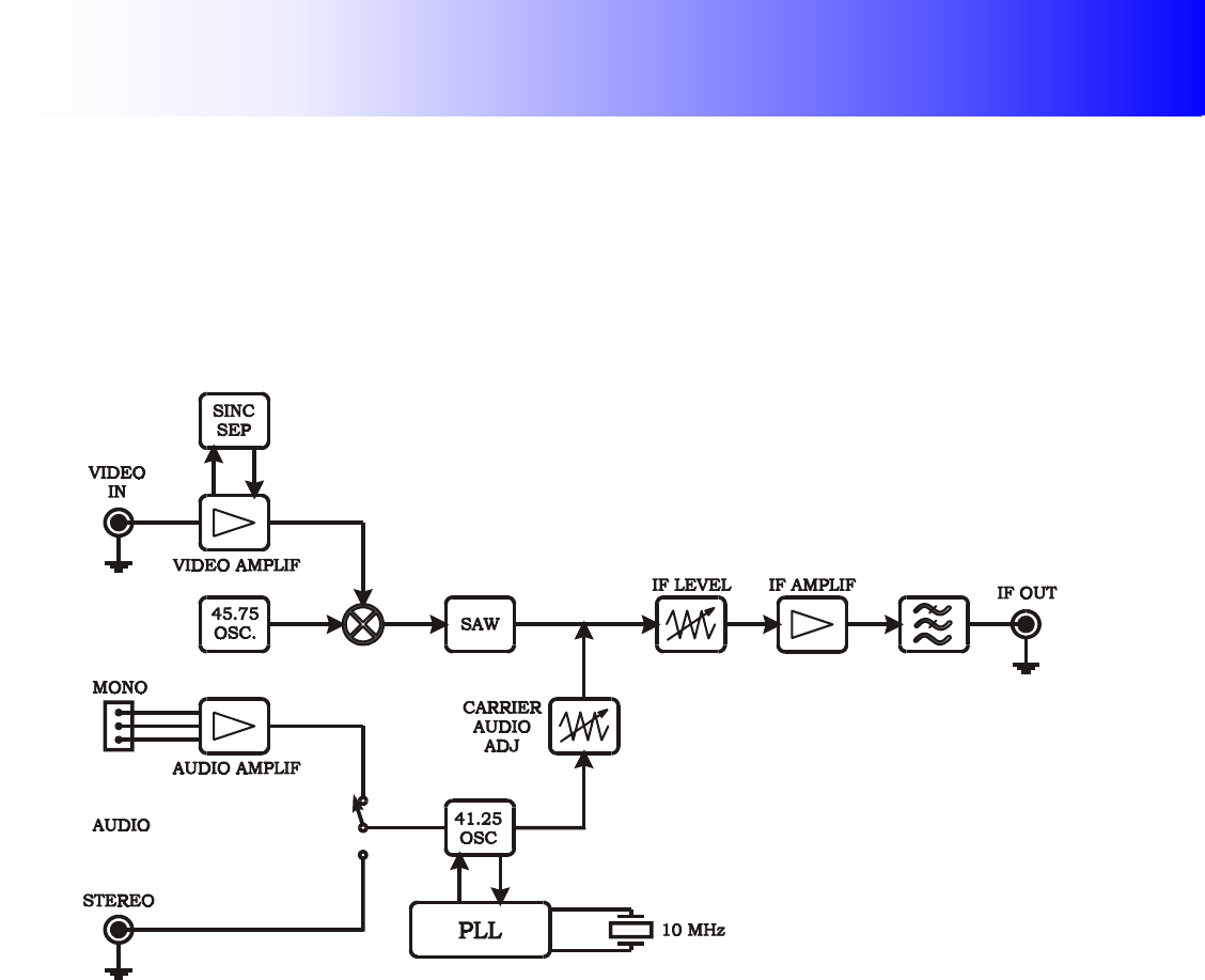
1.2. Block Diagram:
1.3. Technical Description:
1.3.1. Video Modulator:
The transistor Q1 oscillates in the crystal frequency (45.75 MHz - IF video), and the transistor
Q2, with high input impedance, guarantees the isolation to the oscillator Q1 output. The frequency
accuracy is adjusted in the variable inductor L1. The input video signal, with adjustable level in R27
(front panel), is applied to the high impedance input push-pull amplifier formed by transistors Q6 and
Q9. The amplifier output signal modulates in amplitude, in the mixer M1, the video carrier.
The integrated circuits IC18 to IC21 form a group delay predistortion circuit. The syntonized
cells, at the video bandwidth, cause an advancement of 170 ns at 3.58MHz. This video pre-distortion is
inserted in the circuit through jump’s JP5 and JP6. The adjustable attenuator R146 allows equalizing
the video level when the pre-corrector circuit is turned off.
The transistor Q12 receives the video signal, invertes its phase and applies it to the IC7
amplifier. This amplifier causes a non-linear enlargement to the video signal emphasizing the
synchronizing pulses. This signal is clamped in 0.7V by the D5 and is compared to 0.3V (due to diode
D4) in the comparator circuit IC6. In this manner, at the IC6 output, there will be only synchronizing
pulses. These pulses are applied to the IC5 (mono-stable) in the negative transition to generate
clamping pulses. The clamping pulses commute the transistor Q10 that switches the video signal
clamping it to the blanking level through R45. This adjustment allows choosing the point of modulation
in the mixer for a better linearity. If there is lack of clamping pulses, the Q11 transistor commutes,
allowing adjusting through R44 the level of the video carrier without modulation.
The integrated circuit IC9B receives the clamping signal detected through D7, changes its state
and commutes the transistor Q13. It allows switching the external circuits connected to the Automatic
output. The led in the panel shows this operation, when it is green it indicates video on. This circuit
presents about 60 seconds delay time approximately.

Unit 2 – IF Modulator
- 3 -
The video signal peak is detected through IC8 and through IC9 and it is differentiated with the
level adjusted through R45, in order to extract the dc component.
The IC9A output has a dc level related to the video signal not taking into account the
synchronizing pulses. The 100% video measurement is adjusted through R72 in the meter with a video
signal with 100% APL. The C118 e L18 components form an ICPM corrector circuit that allows
correcting a non-desirable phase-shift at the video carrier caused by the modulating signal.
The modulated video carrier is amplified by IC1 and the SAW filter FL1 filters this signal giving
the final characteristics of the desired modulation, i.e., AM_VSB (amplitude modulation with vestigial
side band). The amplifiers IC2, IC3 and IC4 produce the necessary gain to signal, in order to
compensate the losses in SAW filter and deliver a 0 dBm output level. The output signal level is
adjustable by R12 (front panel), which controls the PIN diode conduction (D1). The trimpot R13 limits
the maximum IF output level and the circuit formed by transistor Q19 and capacitor C120 increases
slowly the output level to eliminate high frequency peaks when the equipment is turned on.
The IF signal, after amplification, passes through a low-pass filter, formed by L6, L7, C21, C22
and C23 to eliminate harmonic signals. Part of this signal is sent to the detector circuit formed by
transistors Q3 and Q4 to measure the IF signal in the panel. The trimpot R24 allows adjusting the
reading level through the meter.
1.3.2. Audio Modulator:
The transistor Q14 and associated components generate the audio carrier. The applied voltage
to the varicap diode D10 controls its frequency. The amplifiers IC12 and IC13 increase the signal level
and through the trimpot R108 is applied to the IF amplifier to be delivered at the output. A sample of
this signal is delivered to the “prescaler” IC14 through R108. It divides the signal into 64 and delivers it
to PLL (integrated IC15). The PLL divides again this signal, now into 66, and compares it with a
reference signal in phase, resulting a voltage proportional to the difference of the phase between the
signals; this voltage is filtered and applied to diode D10 to correct the frequency. The reference
frequency for PLL is generated at the integrated circuit itself that oscillates at 10 MHz and divides it
into 1024. The oscillator crystal is found in a thermal chamber, which is controlled by Q15 and by
thermistor NT1, for better frequency stability. The trimmer C90 allows the fine adjustment of this
carrier frequency (41.25 MHz). If the circuit cannot correct the frequency, the transistors Q17 and Q18
are commuted to turn on the frequency error red led.
The audio signal that will cause the modulation in frequency in this carrier may come from the
mono audio input or stereo audio input. It is possible to select it through jump JP3.
The mono audio input circuit has an unbalanced amplifier IC10 and pre-emphasis circuit. It is
possible to turn off the pre-emphasis through jump JP2. The trimpot R92 (front panel) adjusts the
audio level that will cause the correct modulation index. The integrated circuit IC17 and associated
components form a peak detector of audio signal and a trimpot R117 allows adjusting 100% at the
meter for the correct deviation. The battery input (+36V) through D16 and fuse F1 connects through
connector CN2 the power supply FTE017 (optional).
Obs: The circuit diagram is divided into four parts.
Unit 2 – IF Modulator
- 8 -
4. Frontal and Back Panel:
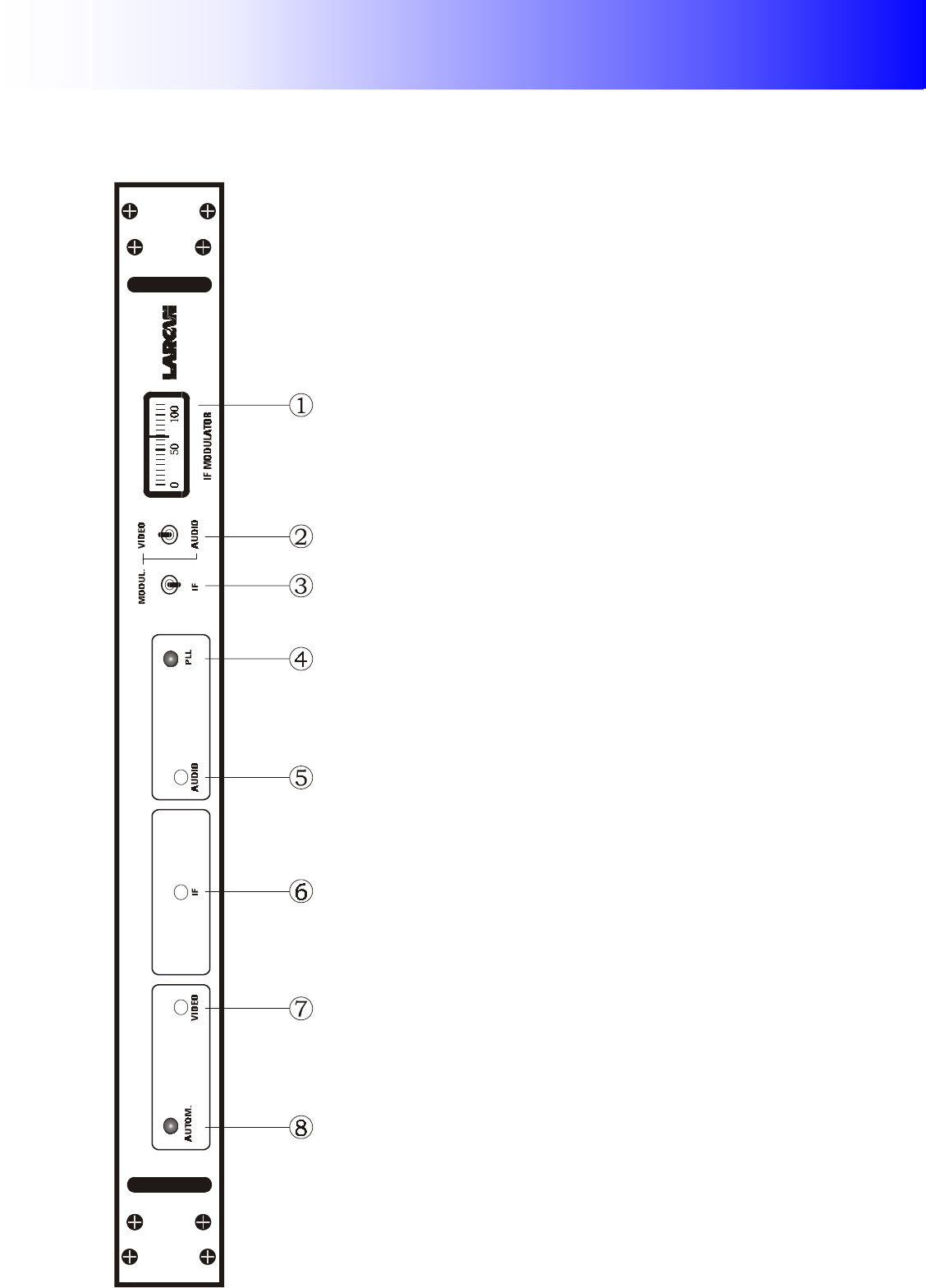
4.1. Frontal Panel:
Each element in the panel has the
following function:
1. Meter: For video, audio and IF
measurements. For a video signal with 100%
APL the meter will indicate 100%. In the audio
position, the measurement of 100% in the
meter will indicate the correct deviation. In the
IF position, the measurement of 100%
corresponds to 0 dBm level in the output.
2. Video/Audio: Measurement selector
switch. This switch selects the video or audio
modulation index when the switch (IF/modul.)
is in the position (modul.).
3. Modul/IF: Measurement selector
swicth. It selects between the modulation index
or the IF level.
4. PLL: Bicolour led, when it is red
indicates that the Audio carrier is out of
frequency.
5. Audio: Audio level adjustment
through trimpot R92.
6. IF: IF level adjustment through
trimpot R12.
7. Video: Video level adjustment
through trimpot R27.
8. Autom: Bicolour Led, when it is red it
indicates video off, when it is green indicates
video on. It takes about 60 seconds delay time
to change from green to red one.
Unit 2 – IF Modulator
- 9 -
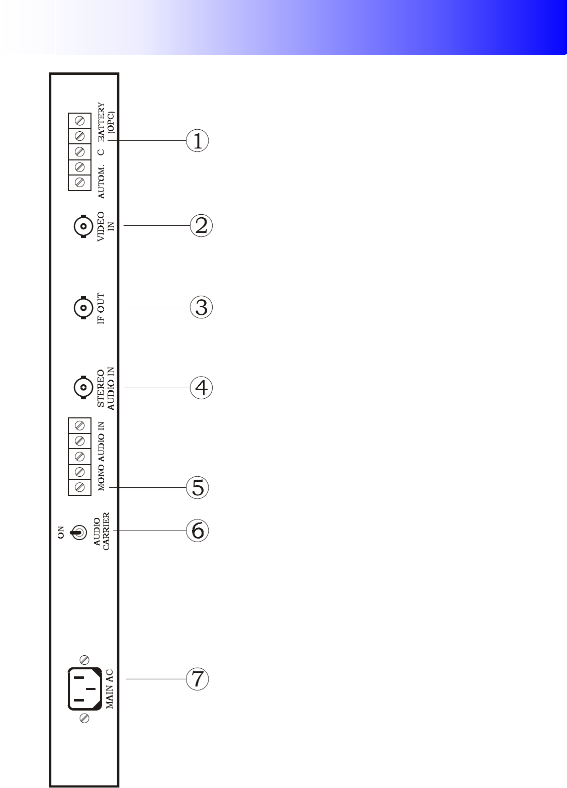
4.2. Back Panel:
Each element in the panel has the
following function:
1. AUTOM, C AND BATTERY (OPC):
- AUTOM: output to external command.
When the video is on, this output is short
circuit to the ground (50mA maximum current).
- C: EXTERNAL CONTROL: Lower output
IF level by ground contact.
- BATTERY (OPC): Battery input +36V
(optional).
2. VIDEO IN: Video input 75 Ohms
impedance (unbalanced) and 1 Vpp level.
3. IF OUT: IF output with 50 Ohms
impedance (unbalanced) and adjustable level.
0dBm Nominal.
4. STEREO AUDIO: Stereo audio input,
75 Ohms impedance (unbalanced), 0dBm level.
5. MONO AUDIO IN: Mono audio input,
600 Ohms impedance (balanced) and 0
dBm/400 Hz level.
6. AUDIO CARRIER: Turn on/off the
audio carrier.
7. MAIN AC: Power supply input 220V.
Unit 2 – IF Modulator
- 18 -
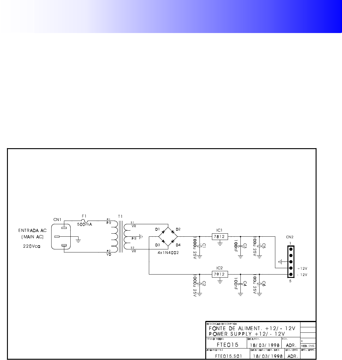
8. Power Supply:
8.1. Function:
The power supply function is to generate +12V and -12V voltage suitable to supply the
modulator.
8.2. Technical Description:
The transformer T1 reduces the input voltage for the rectifiers D1 to D4. The positive and
negative voltage obtained after the rectification and filtering through C1 and C2 are regulated through
IC1 and IC2 to obtain +12V and -12V voltage to supply the Modulator.
8.3. Circuit Diagram FTE015:
Unit 2 – IF Modulator
- 20 -
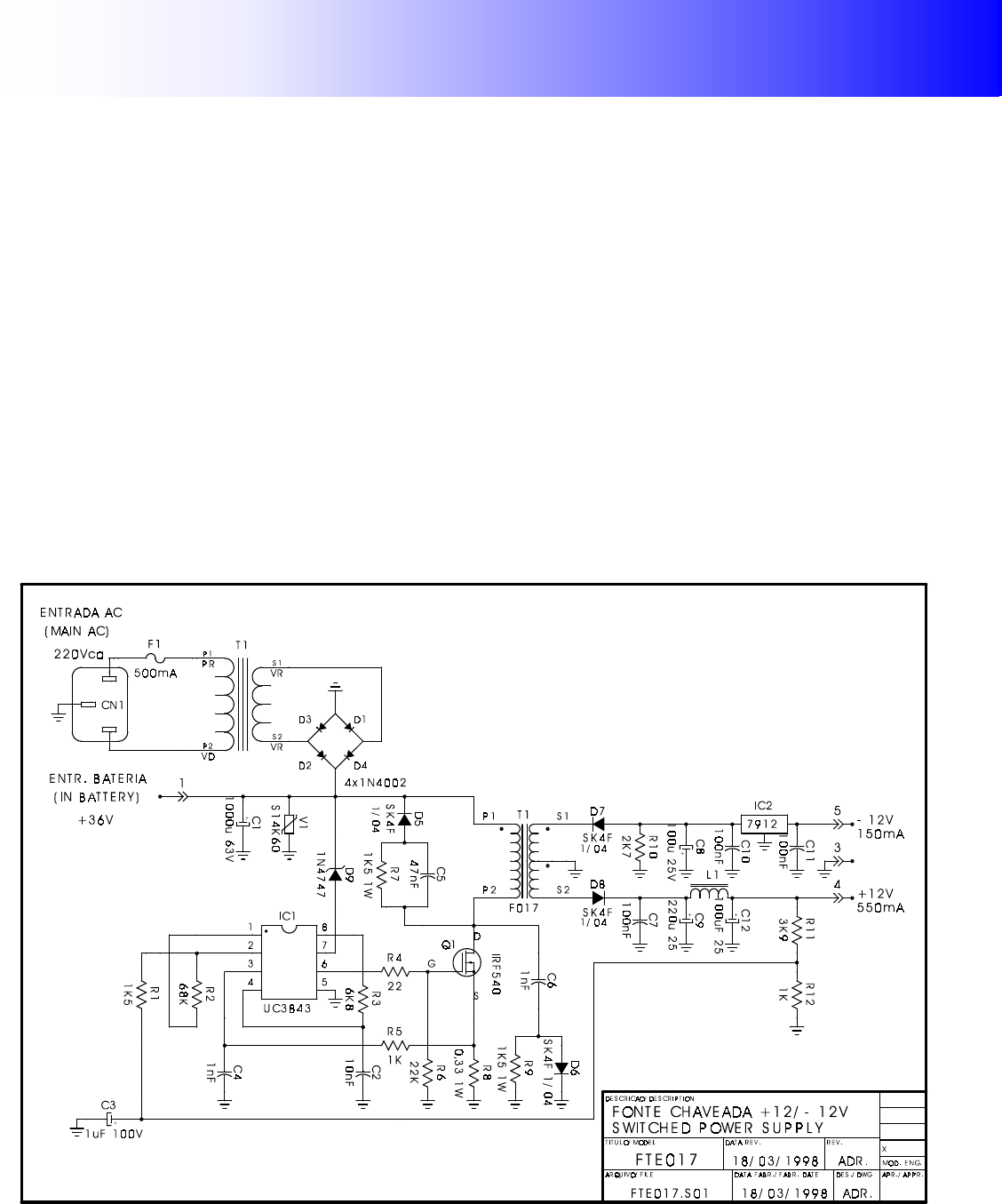
9. Power Supply (optional):
9.1. Function:
The switched power supply has the function to generate +12V and -12V voltages from the input
voltages AC or from the +36V battery (opc).
9.2. Technical Description:
The input voltage, after transformer T2 and diodes D1 and D4, supplies the PWM IC1. If there is
no AC the battery voltage supplies the circuit.
The pulses generated by IC1 commute the transistor Q1 and switch the voltage over the primary
T1 at 25 KHz frequency.
The induced pulses that are in the secondary are rectified by D7 and D8 and filtered by C8 e C9. The
regulator IC2 assures the -12V regulated voltage. A voltage sample after L1 supplies the IC1 control
input, through the divider R11 and R12. The pulses that are generated for IC1 have their width
changed in function of the received sample, canceling, in this manner, any variation in the +12V
voltage. The resistor R9 supplies a sampled voltage related to the current which circulates in the output
to the IC1, pin 3. This input protects the over current, reducing the +12V voltage.
9.3. Circuit diagram FTE017:
Unit 2 – IF Modulator
- 23 -
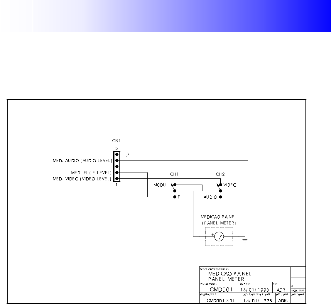
10. Meter Circuit:
10.1. Function:
The meter circuit allows, through the selector switches and meter, the measurements of the
video modulation, audio modulation and the IF level.
10.2. Circuit diagram CMD001:

Unit 3 – Channel UP Converter
- 2 -
1. Channel UP converter:
1.1. Introduction:
This module converts an IF signal, into “a” UHF band channel, maintaining its characteristics
and the same bandwidth.
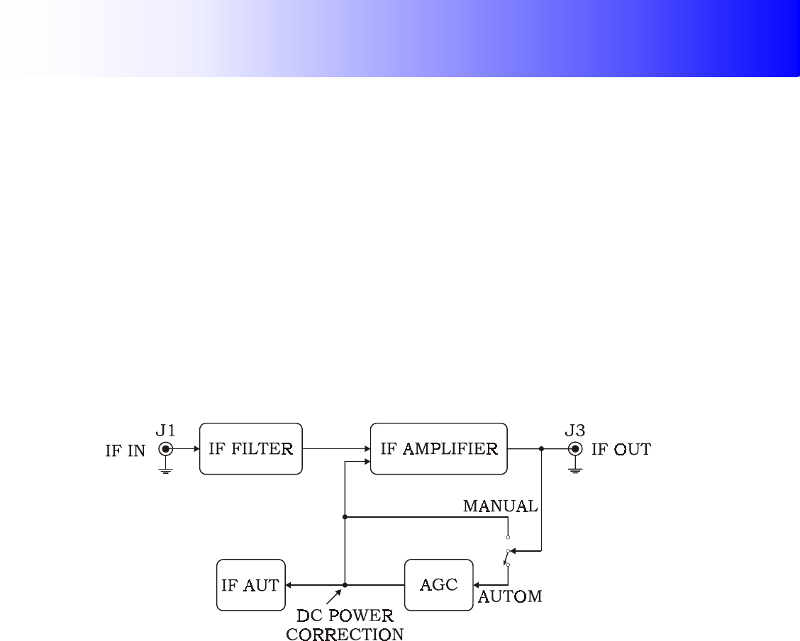
1.2. IF filter and amplifier AGC (for transposer):
The filter and IF amplifier establish the necessary bandwidth to the input signal and supply a
gain in it, maintaining a constant level, through an AGC loop. It is used only in the transposer
equipments.
1.3. IF pre-distortion:
The IF module pre-distortion corrects the intermodulation, the differential gain, the differential
phase and the synchronism compression. This correction is done by pre-distortion on IF level (41-47
MHz). This module is placed after the audio and video modulator and before the channel converter
module.
1.4. Automatic Level Control (ALC):
This module maintains the output peak power at its nominal value, even if there is gain
variation due to the temperature and power supply variations.
It allows a maximum correction of ±1dB.
1.5. Channel converter:
The UHF channel UP converter has an oscillator that is controlled by PLL, whose frequency
operation is selected by DIP switch from the Local Oscillator control board, according to the channel
programming chart.
1.6. Protections/signals:
The channel UP converter has in its front panel a PLL (Phase Locked Loop) alarm led that shows
if the converter is out of the operation frequency.
Unit 3 – Channel UP Converter
- 4 -
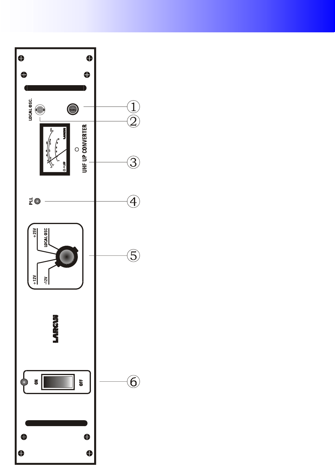
2.2. UP Converter Frontal Panel (for tranmitter):
Each element in the panel has the
following function:
1. FUSE: 2 A fuse.
2. LOCAL OSC: BNC connector used to
monitor the local oscillator by spectrum
analizer.
3. METER: Allows measurements of
+12V, -12V, +25V and Local Oscillator.
4. PLL Led alarm: When the led lights, it
indicates that the local oscillator is out of
frequency.
5. SELECTOR SWITCH: According to
the switch position, the values are indicated in
the meter.
6. ON/OFF SWITCH: this switch allows
turn on and off the UP converter.
Unit 3 – Channel UP Converter
- 5 -
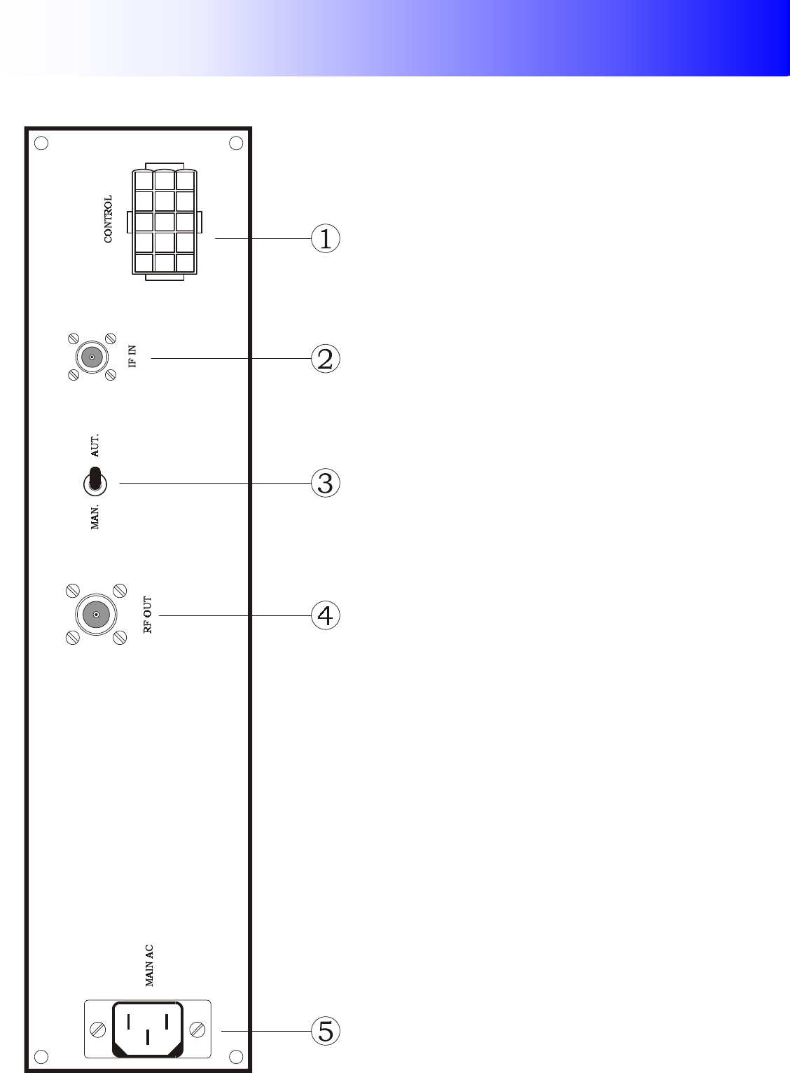
2.3. UP Converter Back Panel (for transposer and transmitter):
Each element in the panel has the
following function:
1. CONNECTOR 15P: main power
supply, commands and measurements.
2. IF IN: IF input connector type BNC.
3. Automatic/Manual selector switch:
Automatic: the equipment operation depends on
the Video or IF signal. Manual: its operation
does not depend on the Video or IF signal.
4. RF OUT: RF output connector type N.
5. MAIN AC: Main AC input 220V.
Unit 3 – Channel UP Converter
- 6 -
3. IF filter amplifier:
3.1. Function:
The IF filter establishes the adequate bandwidth to the input signal and the IF amplifier supplies
the gain for this signal, maintaining a constant level, through AGC loop.
3.2. Technical Characteristics:
Central Frequency __________________________________________________________________________ 44 MHz
Bandwidth __________________________________________________________________________________ 6 MHz
Input and Output impedance ______________________________________________________________ 50 Ohms
Maximum output level ______________________________________________________________________ +3 dBm
Linearity _________________________________________________________________ + or – 0.25 dB in ± 3 MHz
Maximum gain _______________________________________________________________________________ 60 dB
AGC band ____________________________________________________________________________________ 50 dB
Supply ______________________________________________________________________________ +12V at 250mA
3.3. Block Diagram:
3.4. Technical description:
3.4.1. IF Filter:
The input signal is applied by J1. The integrated circuit IC1 amplifies the applied signal to the
IF filter.
The function of the circuit that is formed by C7, L3, C8, C9, L4, C10, C11, L5, C12, C13, C14
and C16 is to determine the IF amplifier operation bandwidth. This filter is adjusted to obtain a 6MHz
bandwidth.
3.4.2. IF amplifier:
The IF signal received from IF filter is, through C17, connected to the adjustable attenuating
loop, that is formed by diodes D2, R9, D4 and D3. After the attenuating loop, the signal is amplified by
the integrated circuit MAR-7 (IC2).
The amplified signal passes through another attenuating loop, formed by diodes and resistors
D5, R14, D7 and D6, and it is connected by the capacitor C28 to the integrated circuit MAR-6 (IC3),
and finally, through capacitor C29, reaches the integrated circuit MAR-7 (IC4).
A sample signal from the output signal is taken from the resistor R45; after, it is amplified by
transistor Q4 and detected by the diodes D10 and D11. The detected signal by the diode D11 is
supplied, by the emitter follower Q3, to check the IF level in the panel.
The integrated circuit IC5-B supplies in its output a dc level, that is the function of the received
signal J1. The diode D1 and L9 act respectively in the polarization of the attenuating loops, altering the
final gain of the IF amplifier. When JP2 is in the AUT position, this dc level is proportional due to the
detected signal by the diode D10, maintaining the IF level constant in the output J3.
The IC5-A output level is the result of input levels voltage comparison between pins 3 and 2.
This way we can determine the operation point of the IF command adjusting R21. Through CN3-1 the

Unit 3 – Channel UP Converter
- 7 -
following circuits are enabled.

Unit 3 – Channel UP Converter
- 12 -
4. IF Pre-distortion linearity:
4.1. Function:
It corrects the non-linearity and/or intermodulation that are generated at the final stage of the
transmitter amplification.
4.2. Technical characteristics:
Frequency band: ______________________________________________________________________ 41 to 47 MHz
Input level: ____________________________________________________________________ -4.0 dBm ± 1.0 dBm
Output level (adj): __________________________________________________________________ + 3.0 dBm (max)
Input/Output Impedance:___________________________________________________________________ 50 ohm
Supply: _______________________________________________________________________________________ +25V
4.3. Technical Description:
IF signal applied to the input J1 is amplified by Q1, and in Q2 is divided in order to supply two
circuits, a linear one and a non-linear one.
The linear circuit has about a 40 ns delay line to compensate the delay caused in the non-linear
circuit. After the delay line, the signal is inserted through trimpot R13 in the adder circuit that is
formed by Q4 and Q5.
The non-linear circuit causes a distortion in the signal through D3 and D4 that have its
conduction region determined by trimpots R11 and R29. This signal, distorted and amplified by Q7 and
Q8, is put in phase by equalizer circuit formed for L11, C29, R40 and R41, again amplified for Q9, via
trimpot R50 and transistor Q10 and finally is added to the linear signal.
The composed IF signal passes by the attenuator circuit, and its level is adjusted by R44, and
amplified by IC1 when it is delivered to output J2.
4.4. Adjustment Procedure:
The signal should be constantly checked by the spectrum analyzer using the red pattern
modulated signal.
1) Insert the circuit in the system when the IF level is about –3.0 dBm in the input and all the
trimpots are in the minimum.
2) Adjust trimpot R44 to 80% of its course approximately, then increase the level in R13 until
the nominal power is reached.
3) Adjust trimpots R11 and R29 in order to cause the needed distortion to cancel the distortion
that comes from the amplifying final stage, adjusting the level of this signal in the trimpot R50 and
compensating the power variation in the trimpot R13, in order to maintain it as a nominal one. Adjust
the inductor L11 to obtain the distorted signal phase inversion that will be inserted in the system.

Unit 3 – Channel UP Converter
- 17 -
5. Automatic Level Control (ALC):
5.1. Function:
The Automatic Level Control corrects the transmitter output peak sync power due to the
variation gain of the amplifiers.
5.2. Technical Description:
This circuit has a total attenuation of 1dB, allowing controlling the power to positive and
negative variation of 0.5dB.
The command occurs through the obtained voltage from the TV monitor through wire identified
by the CAP cord. If the Turn on/turn off switch in the panel is OFF, it allows adjusting the output
power, as it fixes the CP input in 3.7V. We can observe in the circuit the variable attenuator by the
diodes PIN formed by diodes D1, D2 and D3, and capacitors C10, C11 to C14 and resistors R14 and
R15.
The Pin diodes current occurs through the integrated circuit IC1A, by shock CH1. The TV
monitor CAP command voltage supplies the IC1A inverter gate through R1. The integrate circuit IC1A
amplifies this voltage increasing its range from –0.5 to -10V.
The integrated circuit IC1B receives this voltage of –0.5 to -10V by R10, adding it to a pre-fixed
value R7, R8 and R9. This causes the IC1B output variation from –1.5 to -8V approximately, causing
the circuit attenuation to PIN diode, which does not exceed a total variation of 1dB.
The divisor formed by R18, R19 and R20, allows obtaining the reference voltage (REF) to
calibrate the transmitter power in the ALC OFF situation.
5.3. Adjustment Procedure:
a) Turn the switch to OFF position (in the panel).
b) Adjust R19 to a 3.7V reading in a digital multimeter in the output REF pin.
c) Adjust the sweep generator, the detector and the oscilloscope to 0dBm IF frequency, inserting the
circuit.
d) Through CN1 turn on R1 to ground.
e) Verify if the attenuation is inferior to 1dB in the oscilloscope and memorize the response.
f) Through CN1, turn on R1 to -12V.
g) Through R9 adjust the attenuation to 1dB in the oscilloscope.
h) Turn off CN1 and adjust R5 to half of the range in the oscilloscope.
i) Insert the circuit between the modulator and the channel converter.
j) The IF level is adjusted to nominal power when the switch is in OFF position.
k) Change to the ON position, verifying the output power.
Unit 3 – Channel UP Converter
- 21 -
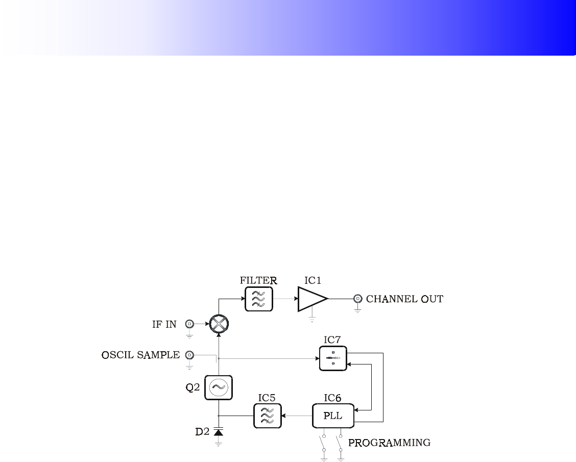
6. Channel UP Converter:
6.1. Function:
The channel UP converter function is to convert the IF frequency (41 to 47 MHz) to a determined
channel in UHF.
6.2. Technical Characteristics:
Input frequency band: ________________________________________________________________ 41 to 47 MHz
Output frequency band:_____________________________________________________________ 470 to 890 MHz
Gain: _________________________________________________________________________________________ 0 dB
Input/Output Impedance: _________________________________________________________________ 50 Ohms
Channel bandwidth: _________________________________________________________________________ 6 MHz
Consume: __________________________________________________________________________ +12V at 150mA
6.3. Block Diagram:
6.4. Technical Description:
The oscillator, transistor Q2, generates a low noise signal in the used frequency band. Its
frequency is determined by the control voltage applied to diode varicap D2. The amplifier IC3 receives
the oscillator signal and provides load isolation and, the amplifier IC2 delivers to the mixer a +17 dBm
level. A sample from the oscillator signal is, through R25, delivered to IC7 prescaler, that divides the
signal into 64 and 65, according to the control that comes from PLL, integrated circuit IC8. PLL receives
the prescaler signal and divides it according to the external programming (1 to 8), and compares it in
phase to a reference signal controlled by crystal generated by the own integrated circuit.
In the integrated circuit output results a proportional voltage that is the phase difference among
the signals. This voltage is filtered by IC5 and applied to diode D2 for the frequency correction
The mixer MX1 receives IF signals and the local oscillator, and generates through the signal
beating the desired channel. The conversion loss in the mixer is aproximately 8dB at most. The signal
after the mixer passes through the channel filter that rejects the local oscillator and the undesirable
product in the conversion. The amplifier IC1 compensates the mixer and the channel filter losses.
6.5. System alignment:
1. Program the oscillator according to the given channel chart and with a multimeter in PT2,
adjust trimmer C21 to a 4.5V reading. The led helps the adjustment, when it is turned off it indicates
that the oscillator is in the desired frequency. In the point meas. at oscillator shows 0.5V level
indicating the RF presence that comes from the local oscillator.
2. Put the sweep generator in the IF band in 41 to 47 MHz, and apply to the IF input, in JP1.
Adjust the channel filter to the maximum gain and a better linearity, with the detector in the channel
output.
Unit 3 – Channel UP Converter
- 28 -
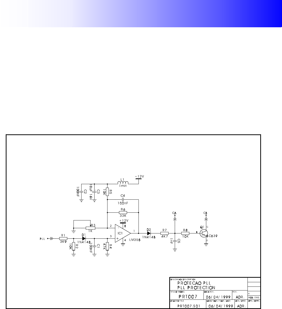
7. PLL protection:
7.1. Function:
This circuit function is to turn off the transmitter.
7.2. Technical Description:
The DC voltage that comes from the channel converter, more precisely from the channel
converter Led diode, is applied to the comparator through diode D1 by resistor R1 and reaches circuit
integrated IC1pin 3.
Through the adjustment in the trimpot R3, we can act in the integrated circuit comparison,
moving pin 1 to high level (operational gain X comparing voltage). Then, through diode D2 this voltage
is applied to CA output (High level) or CB (Low level), by the transistor Q1 collector saturation.
7.3. Circuit diagram PRT007:

Unit 3 – Channel UP Converter
- 30 -
8. UP Converter supply -12, +12 and +24V:
8.1. Function:
The power supply function is to generate -12V, +12V and +24V voltage suitable to supply the UP
Converter.
8.2. Technical Description:
The main AC input voltage is reduced by the transformer T1.
T1 has two secondarie winds, one for the +24V and the second for the +12V and –12V supplies.
D1, D2, D3 and D4 rectifiers the secondary voltage that is filtered by the capacitor C1. IC1 is a
linear regulator that feeds +24V at the output.
D5 and D6 are the retifier diodes for the positive voltage filtered by C4.
IC2 is a linear regulator for the +12V output supply.
In the same manner there are a rectifier and a linear regulator for the negative voltage –12V.