Larcan T5000U 5000 Watt UHF Transmitter User Manual 01 INTRODUCTION rv1
Larcan Inc 5000 Watt UHF Transmitter 01 INTRODUCTION rv1
Larcan >
Contents
- 1. user manual for tx
- 2. user manual for modulator
user manual for tx

Unit 1 – Introduction
- 11 -
2. General Technical Descriptive:
2.1. IF Modulator (for transmitter):
This is the input module. It is a professional audio and video modulator. The audio and video
signals are applied to their respective input for the modulation process in IF (41 to 47 MHz]. The audio
and video input impedances are 600 balanced Ohms and 75 unbalanced Ohms, respectively.
2.1.1. Video processing:
The video signal passes through linearity correction circuits and then is applied to the 45.75
MHz video modulator. There are Synchronizing Separation circuits that generate the auxiliary outputs
to “Automatic Circuits”. The video signal is also applied to a group delay predistortion circuit.
2.1.2. Audio processing:
The Mono-audio signal or stereo base band is applied to the module and modulates a 41.25
MHz audio carrier.
2.1.3 Module output:
Both carriers, audio and video modulated (41.25 and 45.75 MHz), are applied to the “Vestigial
Side Band Filter” (SAW Filter). At the output there is a circuit to control the IF output level.
2.2. UHF UP Converter:
2.2.1. Introduction:
This module converts an IF frequency signal into an UHF band channel, keeping its
characteristics and the same bandwidth.
2.2.2. IF filter and AGC amplifier (for transposer):
The IF amplifier and filter module establishes the adequate bandwidth for the input signal and
supply the gain in this signal, keeping the level constant through an AGC loop.
2.2.3. Technical Descriptive:
The 2nd UHF converter has an oscillator controlled by PLL (Phase Locked Loop Integrated
Circuit), which frequency is selected through the DIP switch from the Oscillator control board. When
the modulated signal in IF is received in the 2nd converter, it is filtered and applied to a mixer. The
result of this mixing is filtered (channel filter) and supplied to the following modules of the equipment,
in the selected channel.

Unit 1 – Introduction
- 12 -
2.3. Amplifier Levels:
2.3.1. Comment/Composition/Origin:
The RTU5000T is composed for eight 625W amplifier modules combined through 3dB hybrid
couplers.
The final modules are drived by an 100W amplifier and 3 dB hibrid couplers as splitters.
All the amplifiers are in solid state.
2.3.2. Protections/Signaling:
Each 625W amplifier has a VSWR protection, temperature and a power limiting circuit.
The output power, VSWR, temperature, current and module voltage can be monitored through a
DB9 connector in the front panel.
In the frontal panel there are the normal power indication (Green Led), low power (red led) and
excessive VSWR (red led). There is, also, a BNC connector for monitoring the output signal of each
module.
At the transmitter output, there is the video and audio power monitoring, antenna VSWR, power
supply antenna, current and voltage and indications of excessive VSWR, excessive filter VSWR, power
supply temperature alarm, video absence, phase fail and others.
There is at the transmitter top, a DB25 connector with transmitter signals, for remote
monitoring.
2.4. Notch filter:
It is used to attenuate out channel spurious generated by the transmitter. It is composed by 11
cavities, 10 are syntonized in the spurious frequencies and 1 in the 2nd harmonic.
Unit 1 – Introduction
- 14 -
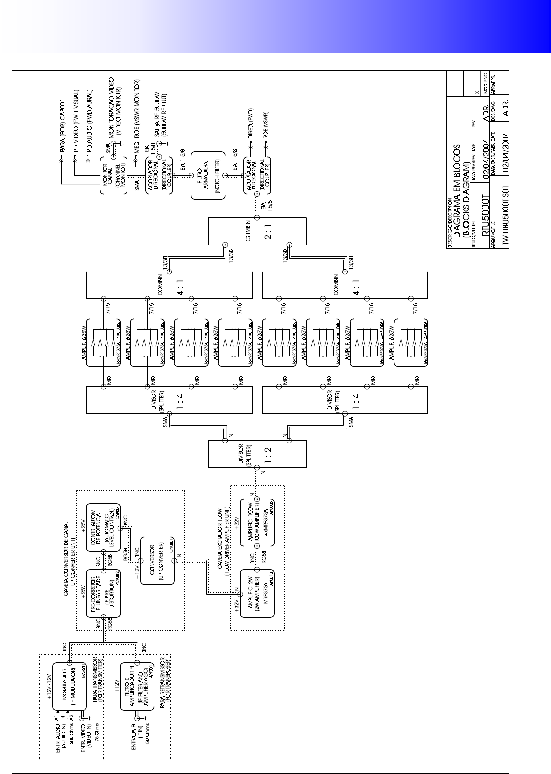
4. Block Diagram:

Unit 4 – UHF 100W Amplifier
- 2 -
1. UHF 100W Amplifier:
1.1. Introduction:
This module amplifies the signal that comes from the channel converter, to the 100 W level,
maintaining its characteristics and the same bandwidth.
1.2. +32V 14A switched power supply:
Its function is to supply the 2 W and 100W modules and also the protection circuits that
compose the unit.
It is necessary a 220VCA transformer with 35V 15 A output to supply it.
Its efficiency is about η = 80%.
1.3. 100W Amplifier protections:
For these functions, we have:
VSWR Circuit: it protects the amplifier module transistors, when the output stationary wave is
superior to 4%. This circuit acts in the output transistors gate.
Temperature Circuit: it acts in the output transistors gate when the heat sink temperature is above
56°C.
Over voltage Circuit: this circuit avoids that voltages upper than 32V supply the amplifier modules.
When this circuit starts operating the 15 A F1 and F2 fuses damage.
1.4. Power detecting and power limiting protection:
This detector function is to transform a RF signal sample in voltage DC. This voltage, that is
proportional to the RF signal, reaches the power limitig circuit to protect the amplifier modules.
1.5. Amplifier stages:
2 W and 100W amplifier modules are used. For this amplifier stages, we use 1 transistor
MRF373A for 2W and 4 transistors MRF 373A for 100W. Its gain is about 50 dB in class AB.
Unit 4 – UHF 100W Amplifier
- 3 -
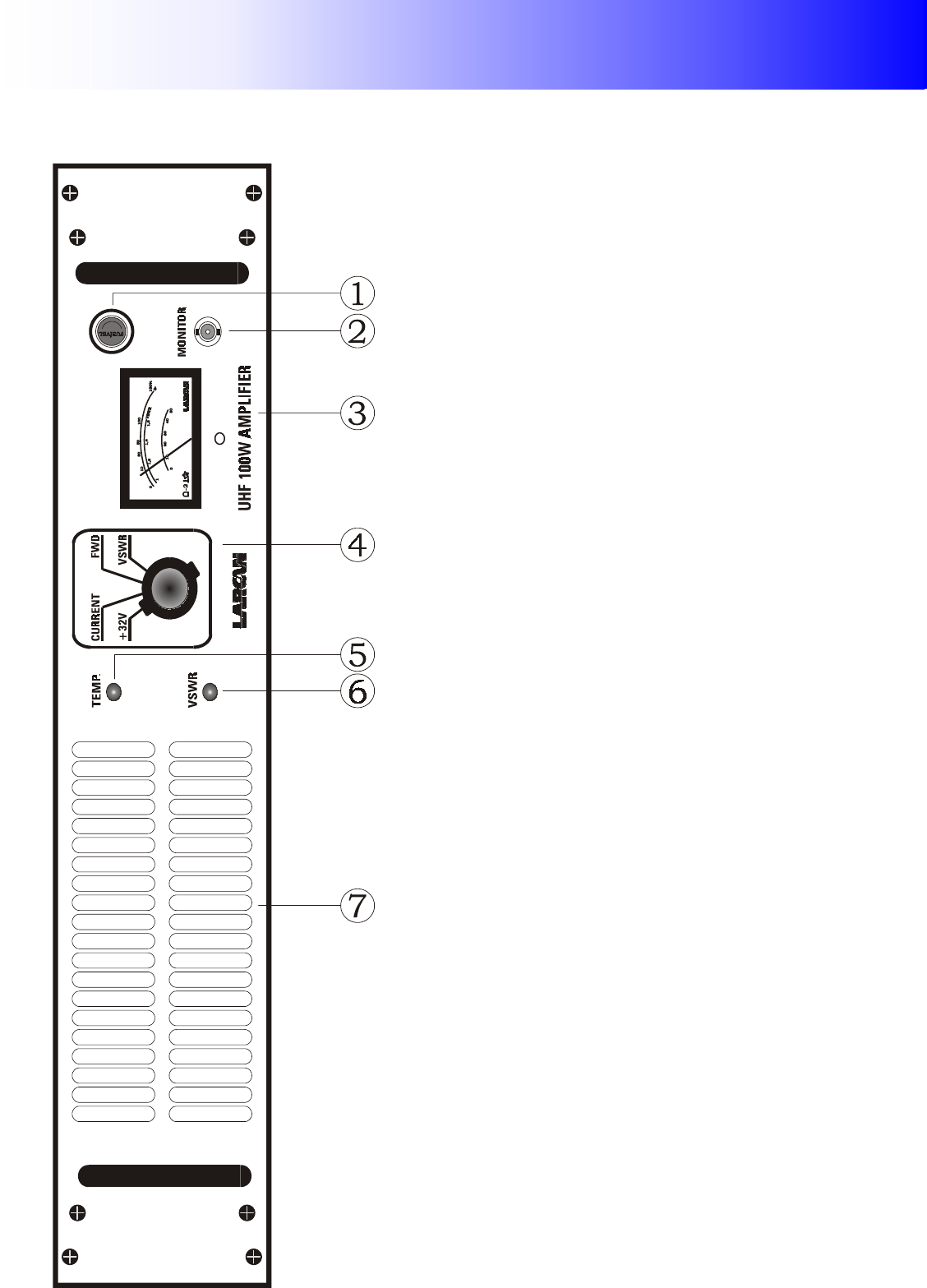
2. Frontal and back panel:
2.1. Frontal Panel:
Each element in the panel has the
following function:
1. Circuit Breaker: Protection circuit
breaker 7 A.
2. Monitor: Connector (BCN) is used to
monitoring the RF output signal in the
spectrum analizer.
3. Meter: it allows visualizing +32V
measurements, current, forward power and
VSWR, according the selector switch position.
4. Selector switch: according to the
switch position, the values are indicated in the
meter.
5. Temperature Led alarm: When the
led lights, it indicates an over temperature.
6. VSWR Led alarm: When the led
lights, it indicates an exceeding VSWR.
7. Air input: there is a fan inside it,
which cools the final amplifier heat sink.
Unit 4 – UHF 100W Amplifier
- 4 -
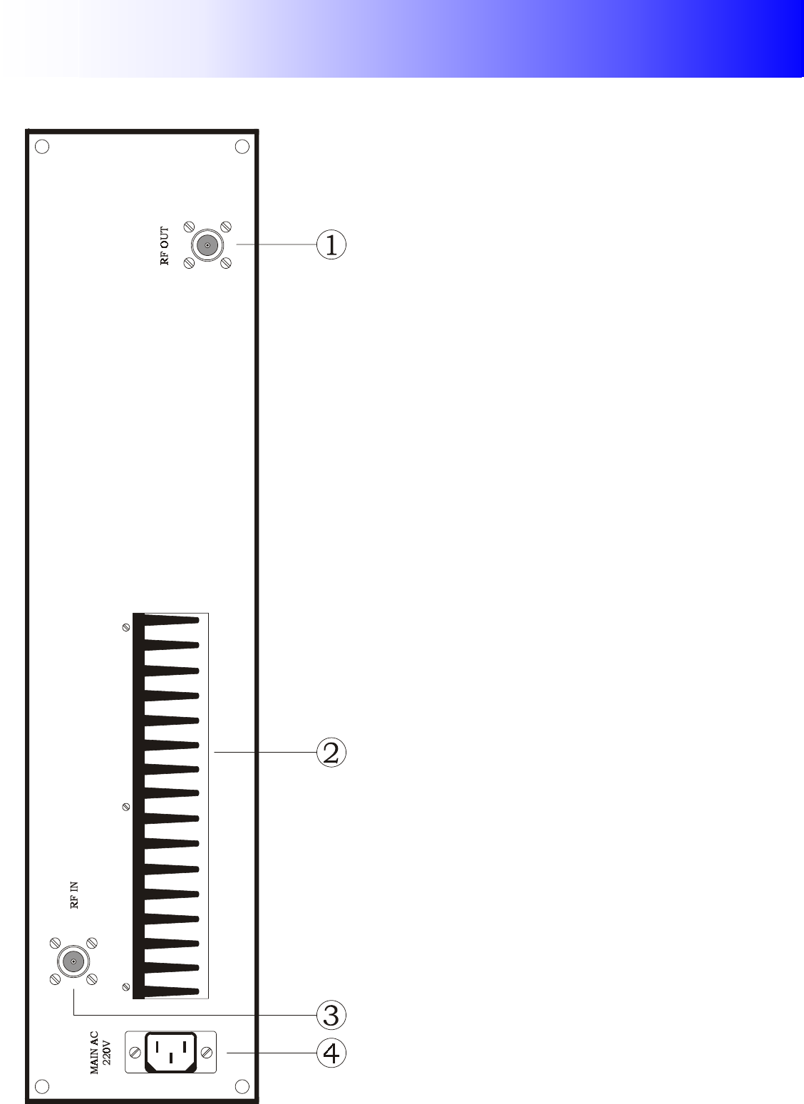
2.2. Back Panel:
Each element in the panel has the
following function:
1. RF OUT: RF signal output by via
connector N.
2. AIR OUT: The air enters through the
frontal panel, cools the heat sink and the hot
air leaves by the back panel.
3. RF IN: RF signal input by connector
N.
4. MAIN AC 220V: main AC power
supply 220V.

Unit 4 – UHF 100W Amplifier
- 5 -
3. Switched power supply +32V 14A:
3.1. Function
The function of this is to provide 32Vdc with 14 A to the 100W amplifier module.
3.2. Technical characteristics:
Input voltage: __________________________________________________________________ 35Vca ± 10% to 15 A
Output voltage: ____________________________________________________________ 32Vdc to 14 A maximum
3.3. Technical description:
The integrated circuit IC1 operates as PWM (Pulse Width modulator).
In the IC1 pins 11 and 12 , we have the IC supply voltage that comes from zener D1. The power
supply Soft Start is effected by capacitor C9 1µF with resistor R7 10K, acting in pin 4 of IC1. The power
supply oscillation is determined by capacitor C14 and by resistor R8. In pin 9 and 10 from integrated
circuit TL494 we have pulses that will activate the current drivers Q1 and Q2.
This sample is transferred to transformer T1 that will activate, through its secondary, the FET’s
Q5 and Q6. D6 is a fast diode used in switching to avoid reverse voltages in the FET’s. T2 function is to
isolate switched power supply from the continuing voltage and also, with capacitors C18, C19, C20,
C21 and C22 form the filter LC from the power supply. The Shunt RSC is a resistor of low ohm value,
made of nickel/chrome which value does not vary due to the circulating current. The power supply
module formed by R12 and R11//R10 determines the power supply voltage. The sample of this voltage
acts in pin 1 from integrated circuit TL494. Any variation in the output voltage is compensated in pin 1
that acts in the pulse width or shut in pins 9 and 10. The resistors R5 and R6 and capacitor C13 act in
the power supply loop. This means the quickness with which the output maintain constant due to the
current sudden variation. The over current circuit is formed by Q3, Q4, D4, R13 and associated parts,
that act in pin 1 from IC1, decreasing the output voltage to currents upper than 23 A.
The capacitors C1 to C4 and C5 to C7 form an input filter CA after the rectification, and C5 to
C7 are 220 µF capacitors of special manufacture (HFC). These capacitors are used for switching and
cannot be substituted for any other type of capacitors.

Unit 4 – UHF 100W Amplifier
- 10 -
4. 100W UHF amplifier protection:
4.1. Function:
The function of this module is to protect the 100W module, which is formed by VSWR,
temperature, over voltage and the power supply limiting circuits.
4.2. Technical Description:
The VWSR sensor protection is calibrated in the plant to be put in action when 4% of stationary
wave occurs. The voltage that comes from the VSWR detector acts in the IC3B comparator, through pin
5. Pin 6 has its voltage calibrated previously in the plant for 4% of VSWR, acting in the FET’s gates.
NTC, R17, also acts in the IC4B comparator, through pin 5 with a voltage that comes from the
power module through R18 and R21. Q1 puts in action the IC output, as well as it indicates the TL
(Temperature Led) when it is turned on.
The power supply over voltage is produced by IC2, SCR1, SCR2, F1 and F2. When any anomaly
occurs, IC2 pin 8 has a high level that discharges SCR1 and SCR2, burning the 15A F1 and F2 fuses.
The RF power limiting compares the DC voltage that comes from the Protection detector and the
voltage limitat by IC5 pin 5 with a fixed calibrated voltage in the plant IC5 pin 6, acting in the FET’s
bias gates when the output voltage reaches nominal +10% (similar to the VSWR protection). The
comparing voltage happens from the rectification from a final module RF sample, which is always
proportional to the output power.
Unit 4 – UHF 100W Amplifier
- 14 -
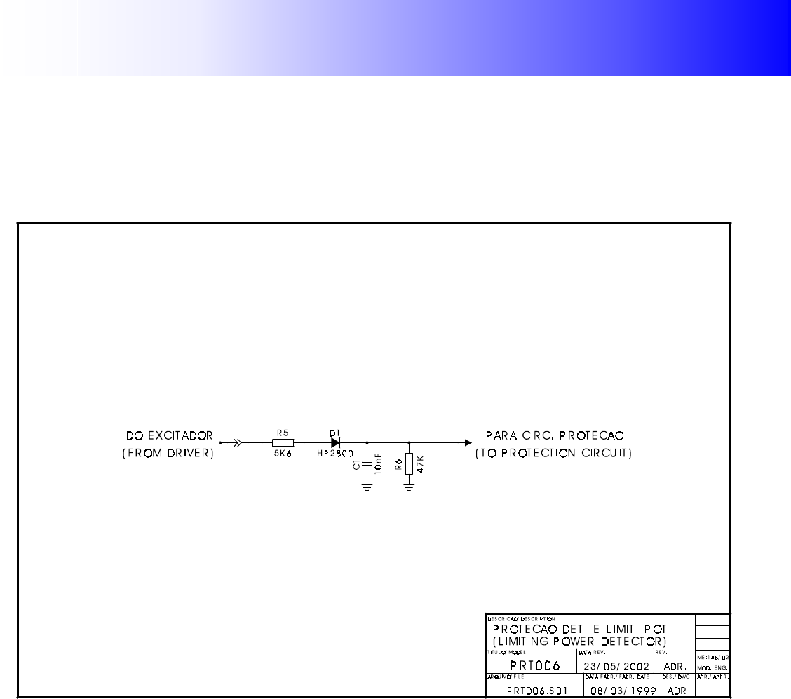
5. Power detecting and power limiting protection:
5.1 Function:
Its function is to protect the output transistors from the excessive signal applied to the input.
5.2. Circuit Diagram PRT006:

Unit 4 – UHF 100W Amplifier
- 16 -
6. 2W UHF Amplifier:
6.1. Function:
The 2W UHF amplifier stage amplifies the channel converted to 2W maximum level.
6.2. Technical characteristics:
Gain: ________________________________________________________________________________________ 30 dB
Supply: _____________________________________________________________________________________ +32Vdc
Total current: ___________________________________________________________________________________ 1 A
6.3. Technical Description:
This module is composed of driver amplifier IC1 and the final amplifier Q1.
Trimpot R4 sets the quiescent current of Q1 and D1 and allows controlling the output power for
protection purposes.
At the input, there is a local oscillator filter TLE, C4 and C5.

Unit 4 – UHF 100W Amplifier
- 19 -
7. 100W Output amplifier:
7.1. Function:
Its function is to amplify the power that comes from the 2W amplifier to 100W output level.
7.2. Technical characteristics:
Power supply: ________________________________________________________________ 32Vdc 11 A maximum
Input power: ________________________________________________________________________ 2W (Peak Sync)
Output power:____________________________________________________________________ 100W (Peak Sync)
Gain: _______________________________________________________________________________________ 18.8 dB
Setting Temperature: __________________________________________________________________________ 56°C
7.3. Technical Description:
The UHF 100W amplifier is formed by the combination of two 50W amplifiers.
At the input and output there are two 3 dB hibrid couplers with the rejection loads R1 and R14.
The signal splitted by the 3 dB coupler input feeds the two 50W amplifiers through C1 and C2.
At the input of esch 50W amplifier there is a balun L1 and L2 that splittes the signal again for
two transistor Q1, Q2 and Q3, Q4 respectively.
The amplified signals through the baluns L5 and L6 are combined in the final 3 dB coupler with
the coupling capacitors C28 and C34.
The bias circuit is formed by resistores R12, R13 and zener diode D3 that generates a +15Vdc.
Through trimpot’s R6 and R7 the bias voltage for the transistor’s gate are adjusted.
The diode D1 and D2 allow a protection, for the amplifier, reducing the bias voltage and the gain
of the amplifier.

Unit 5 – UHF 625W Amplifier
- 2 -
1. 625W amplifier:
1.1. Introduction:
This module amplifies the RF power that comes from the 3dB hibrid splitter to the 625W level.
1.2. +32Vdc 25 A switched power supply:
Its function is to supply the 160W amplifier and also the protection circuits that compose the
module.
The input voltage is about 50Vdc, obtained from a 36Vac three-phase rectifyng supply.
1.3. Protections and Monitoring:
For these functions, we have:
VSWR Circuit: it protects the amplifier module transistors, when the output VWSR is superior to 4%.
This circuit acts in the output transistors bias gate.
Temperature Circuit: it acts in the output transistors bias gate when the heat sink temperature is
above 56°C.
Forward RF power limiting circuit: it acts in the output transistor bias gates when the RF output
power exceeds the pre-fixed value, this way limiting the maximum power.
1.4. Supply fuses:
In this circuit there are four 15 A fuses, one for each 160W amplifiers.
1.5. Amplifier stages:
Four amplifier modules with 160W each are used in parallel. Each 160W amplifier module has
four LDMOS transistors MRF373A in parallel. Its gain is about 20 dB in class AB.
Unit 5 – UHF 625W Amplifier
- 3 -
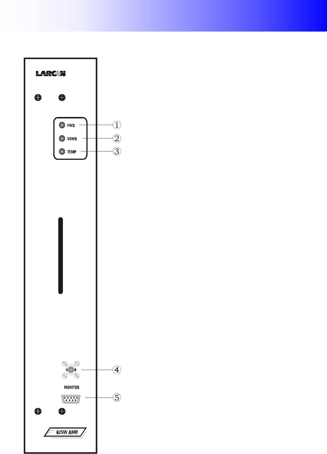
2. Frontal and back panel:
2.1. Frontal panel:
Each element in the panel has the
following function:
1. FWD: when the red led lights, it
indicates power than less 3dB in relation to the
nominal; when less than one lights, it indicates
nominal power.
2. VSWR: When the led lights, it
indicates an exceeding VSWR.
3. TEMPERATURE: When the led lights,
it indicates an over temperature.
4. MONITOR: Connector (BCN) is used
to monitoring the RF output signal in the
spectrun analizer.
5. DB9 Monitoring: it allows monitoring
the following functions:
Pin 1: Ground
Pin 2: IC2 – current power supply 2
Pin 3: VC2 – voltage power supply 2
Pin 4: VSWR measurement
Pin 5: DV (+12V)
Pin 6: IC1 – current power supply 1
Pin 7: VC1 – voltage power supply 1
Pin 8: Forward RF power measurement
Pin 9: Temperature measurement
Unit 5 – UHF 625W Amplifier
- 4 -
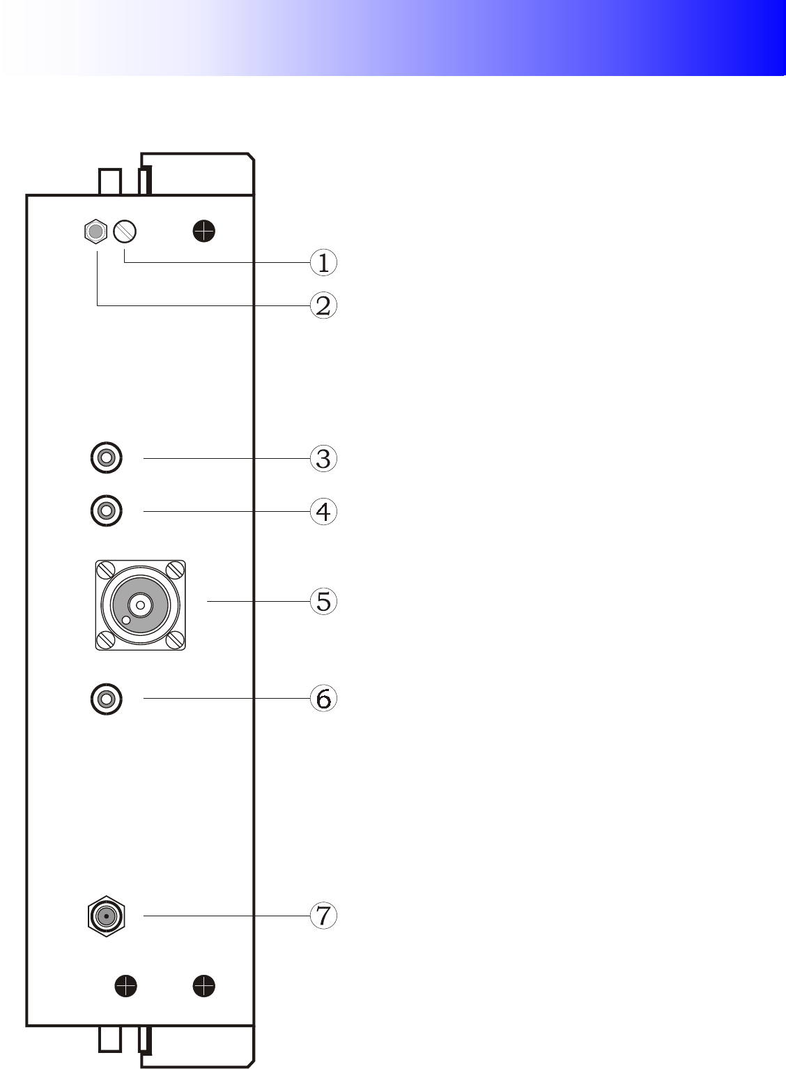
2.2. Back panel:
Each element in the panel has the
following function:
1. FIXING SCREW: A screw-nut is
attached to it, to tie the module to the rack,
where the screw-nut starts the power shut off
(2).
2. POWER SHUT: Off inter lock that
acts on power supply shutting off power.
3. RED PLUG: +46Vdc power supply
input to power A.
4. RED PLUG: +46Vdc power supply
input to power B.
5. RF OUT: RF signal output.
6. BLACK PLUG: Ground.
7 RF IN: RF signal input.

Unit 5 – UHF 625W Amplifier
- 5 -
3. +32V 25A switched power supply:
3.1. Function:
There are two +32V 25 A switched power supplies, each one supply two 160W amplifier
modules.
3.2. Technical Characteristics:
Input voltage: _____________________________________________________________________ +46Vdc with 18 A
Output voltage: _____________________________________________________________________ +32Vdc to 25 A
Module Current: _____________________________________________ 11.5 A with black video + Audio Carrier
3.3. Technical description:
The integrated circuit IC1 operates as PWM (Pulse Width modulator).
In the IC1 pins 11 and 12 , we have the IC supply voltage that comes from zener D1. The power
supply Soft Start is performed by capacitor C9 1µF with resistor R9 10K, acting in IC1 pin 4. The power
supply oscillation is determined by capacitor C14 and by resistor R12. In pin 9 and 10 from integrated
circuit TL494 we have pulses that will activate the current drivers Q1 and Q2.
This pulses are transferred to transformer T1 that will activate, through its secondary, the FET’s
Q3 and Q4. D7 is a fast diode used in switching to avoid reverse voltages in the FET’s. T2 function is to
isolate switched power supply from the continuing voltage and also, with capacitors C24, C25, C26 and
C27 form the filter LC. S1 is a current sample sensor. R25 adjusts the current to be measured in
connector CN1:4.
The over current protection is performed by R26, acting in IC2B pin 6. The voltage at IC2B pin
7, feeds the IC1 control pin 4, reducing the output voltage.
The voltage divider formed by R14 and R15//R16 determines the power supply output voltage.
This voltage sample acts in pin 1 from integrated circuit TL494. Any voltage variation in the output is
compensated in pin 1 that acts in the pulse width present on pins 9 and 10. The resistors R6 and R7
and capacitor C10 act in the power supply voltage feed back.
The capacitors C1 to C3 and C4 to C6 form an input filter CA after the rectification, and C1 to
C3 form the output filter.

Unit 5 – UHF 625W Amplifier
- 9 -
4. Amplifier protection:
4.1. Function:
This module function is to protect the final amplifier modules against excessive VSWR,
temperature and excessive RF power.
4.2. Technical Description:
Directional Coupling detectors in the amplifier module output gives information about the
Forward RF Power and VSWR.
The voltage proportional to the Forward RF Power supplies IC5A buffer amplifier integrated
circuit. This amplifier output supplies two comparing circuits, IC5B and IC2A. The integrated circuit
IC5B acts as a power limiting be that, if the forward RF power exceeds the pre-fixed value by trimpot
R31, transistor Q1 is conducted by diode D3 and resistor R39, removing the bias from the final
amplifier gates. The integrated circuit IC2A compares the forward RF power to a –3dB adjusted value by
R10, lightning the forward green Led in the panel. The integrated circuit IC2B is an inverter amplifier,
be that, when the forward RF power drops below to –3dB, its output reaches +12V lightning the forward
red Led in the panel.
VSWR proportional voltage supplies IC4A buffer amplifier integrated circuit. IC4A output
supplies IC4B comparing input, and also the monitoring in the panel by resistor R1.
If the RF signal exceeds the pre-fixed value by R24, the VSWR Led lights in the panel and
transistor Q1 conducts through diode D5 and resistor R39, removing the bias from the output amplifier
transistor gates.
A temperature sensor protects the temperature. It provides a proportional voltage to the
10mV/°C monitored temperature, be that, for 50°C we have 500mV. Through IC3A buffer amplifier,
this voltage is compared to a pre-determined value by trimpot R17 and also sent to the frontal panel.
IC3B integrated circuit lights “temperature” Led in the panel and by transistor Q1, diode D4 and
resistor R39, is removed the bias from the final amplifier transistors.
Diodes D1 and D2 and the fixed voltage regulator IC1, are responsible for generating the +12V
voltage that supplies several IC’s from the protection circuit.
Unit 5 – UHF 625W Amplifier
- 13 -
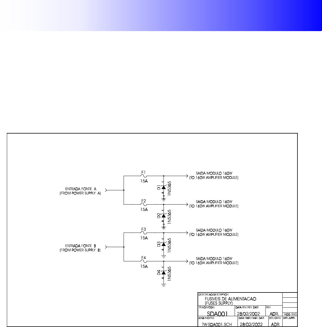
5. Supply fuses:
5.1. Function:
This circuit protects the both power supplies against short circuit zener diodes D1 to D4,
perform the over voltage protection.
5.2. Technical Description:
The +32Vdc voltage of each internal power supplies the power amplifier modules by 4 fuses of
15 A each, F1 and F2 for power supply A and F3 and F4 for power supply B.
5.3. Circuit diagram SDA001:

Unit 5 – UHF 625W Amplifier
- 15 -
6. 625W final amplifier:
6.1. Function:
Its function is to amplify the power that comes from splitter 1:8 to a 160W output level.
6.2. Technical characteristics:
Output power: _____________________________________________________________________ 160W Peak Sync
Gain: ________________________________________________________________________________________ 20 dB
Activating temperature: ________________________________________________________________________ 56°C
6.3. Technical Description:
The UHF 160W amplifier is formed by the combination of two 80W amplifiers.
At the input and output there are two 3 dB hibrid couplers with the rejection loads R1 and R14.
The signal splitted by the 3 dB coupler input feeds the two 80W amplifiers through C1 and C2.
At the input of each 50W amplifier there is a balun L1 and L2 that splittes the signal again for
two transistor Q1, Q2 and Q3, Q4 respectively.
The amplified signals through the baluns L5 and L6 are combined in the final 3 dB coupler with
the coupling capacitors C28 and C34.
The bias circuit is formed by resistores R12, R13 and zener diode D3 that generates a +15Vdc.
Through trimpot’s R6 and R7 the bias voltage for the transistor’s gate are adjusted.
The diode D1 and D2 allow a protection, for the amplifier, reducing the bias voltage and the gain
of the amplifier.
Unit 6 – Cabling and attributes
- 7 -
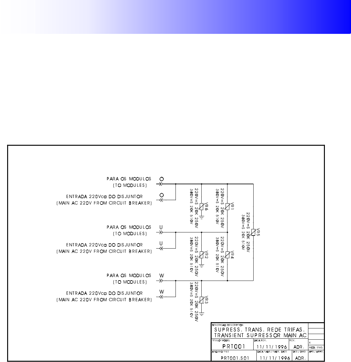
2. Transient suppressor main AC:
2.1 Function:
Its function is to protect against voltage peaks in the three-phase AC, caused by atmospheric
and transient discharges.
2.2 Technical Description:
This circuit is composed of three varistors: VR1, VR2 and VR3. The VR1 varistor is
interconnected phase to phase and the varistors VR2 and VR3 are interconnected phase and ground.
2.3. Circuit diagram PRT001:
Unit 6 – Cabling and attributes
- 9 -
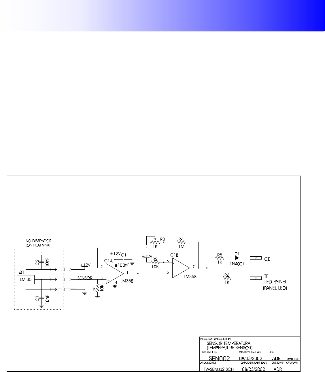
3. Temperature sensor:
3.1 Function:
Its function is to protect the diode banks of two main power (A and B), as well as the balanced
load if there is ventilation fail.
3.2 Technical Description:
The integrated circuit IC1A is an operational IC acting as an input buffer. The “buffer” output is
compared to pin 6 of the integrated circuit IC1B, where trimpot R3 determines the sensor disarm point.
The disarm adjustment to 56°C is made in the plant.
Pin 7 acts at CE, at exciter disarm, as well as at TF Led, at power temperature or balanced load.
Temperature sensor Q1 is mounted in each heat sink (power A and B and balanced load) in
order to accomplish the function.
In its output we have 10mV/°C, be that, if we have 50°C, this component voltage output will be
500mV.
3.3. Circuit Diagram SEN002:

Unit 6 – Cabling and attributes
- 11 -
4. TV Monitor:
4.1. Function:
The TV monitor function is to detect the output RF signal and final amplifier, providing the video
carrier output power reading and audio carrier and the video signal monitoring that have been
transmitted.
4.2. Technical Description:
The obtained signal through the directional coupler supplies the monitor input, by connector J1.
The resistors R14 and R15 provide 50 Ohm termination for interconnecting cabling. The diodes
D2 and D3 function is to detect the RF signal and they are polarized to a better linearity through R1,
R2, D1, C1 and L1. The linearity adjustment is made by R4.
The detected signal by D2 supplies the detector peak circuit via R4, formed by IC1, IC2A and
associated components in order to obtain the output peak sync power reading from the power stage.
Through R12, the reading is adjusted to the panel. The detected signal by D3, after passes by
Q1, that provides high impedance to D3, it supplies the 4.5 MHz filter formed byL2, C26, C27, C12,
R18 and R19. The filter can be short cut by CH1.
The video signal through trimpot R20, supplies the video IC6 that through R38 shows a 75 Ohm
output impedance.
4.3. Adjustment Procedure:
a) The trimpot R12 is put at half course.
b) The directional coupler detector is adjusted in order to obtain the reading in the meter and
directivity.
c) R20 is adjusted till we obtain video 1Vpp in the oscilloscope that is terminated in 75 Ohm.
d) R35 is adjusted to 0Vdc in the blanking level.
e) Through R2, the video linearity is adjusted.
f ) Through L2 and R18, the filter is syntonized for 4.5 MHz minimum value over the video.

Unit 6 – Cabling and attributes
- 16 -
5. Meter Panel:
5.1 Function:
Its function is to monitor the equipment, signalizing the measurement in the meter, according to
the select switch, also by alarm Led.
5.2. Technical Description:
There is a “signalizing” (network) in the equipment superior frontal side, that when it switches
on the equipment general breaker, that is in the left back base, it lights and signalizes the power
supply; there is a Turn on/Turn off switch, that allows turning on/turning off all the equipment, after it
receives the video signal; next to the Turn on/Turn off switch, there is another switch, ALT (Automatic
Level Control), that when it is turned on, it corrects the equipment final power in + or – 5%.
According to the select switch position, the values that are indicated in the measurement meter,
allows visualizing the following measurement: Power A, Power B, Current A, Current B, FWD Visual,
FWD Aural and VSWR.
There are also in the panel the following Leds:
1- VIDEO IN: it indicates when the video signal is present;
2- P/S TEMP A: it indicates when the temperature is too high in the power A rectifying bridge;
3- P/S TEMP B: It indicates when the temperature is too high in the power B rectifying bridge;
4- LOAD TEMP: it indicates when the temperature is too high in the rejection load;
5- VSWR FILTER: it indicates when the reflected RF power is excessive in the filter;
6- VSWR ANT: it indicates when the reflected RF power in the antenna is excessive;
7- PHASE FAIL: it indicates when there is phase absence in the system.
Finally there is a reset switch, that when it is pressed, unlocks the protection system previously
shown, causing the equipment starts working again, unless it has any other problem.

Unit 6 – Cabling and attributes
- 20 -
6. Remote monitoring:
6.1 Function:
The remote monitoring function is to generate the equipment main parts information to external
interface which may be a modem, a phone line, a micro-computer or others; the output transmitter
provides DC voltage levels and should have a convertion from analogue to digital externaly.
This way we can verify the equipment performance or anomalies at distance.
6.2. Pins:
1. GND: Ground;
2. TSCAP: Forward visual power measurement by TV monitor;
3. TSAUD: Forward aural power measurement by TV monitor;
4. TSMR: VSWR Antenna Measurement by command board (IC3A pin 1);
5. NC;
6. NC;
7. NC;
8. NC;
9. NC;
10. NC;
11. NC;
12. PRT: Drives commuting inhibiting by the central rack command board;
13. NC;
14. AUTC: Video absence/ video presence;
15. TSTFA: P/S temp A (2.5KW) temperature sensor;
16. TSTFB: P/s temp B (2.5KW) temperature sensor;
17. TSTCA: Rejection load temperature sensor;
18. TSRF: VSWR in the filter comes from the central command board by Q6 collector (detector +);
19. TSLRA: Antenna VSWR comes from the central command board by Q5 collector (detector -);
20. TSLF: Phase fail from the central rack command board in the Q7 collector;
21. TSCOM: Drives commuting, commuting led indication by IC3 pin 8;
22. NC;
23. NC;
24. NC;
25. NC;