Lattice Semiconductor MOD65412 60GHz Module set for Gigabit-Class Wireless Infrastructure Application User Manual MOD65412 Wireless Link Module Set
Lattice Semiconductor Corporation 60GHz Module set for Gigabit-Class Wireless Infrastructure Application MOD65412 Wireless Link Module Set
Manual and Installation Guide

MOD65412 Wireless Link Module Set
Preliminary Data Brief
SB-DB-02006-0.80
February 2018

MOD65412 Wireless Link Module Set
Preliminary Data Brief
2 © 2018 Lattice Semiconductor SB-DB-02006-0.80
All rights reserved. CONFIDENTIAL
Copyright Notice
Copyright © 2018 Lattice Semiconductor Corporation. All rights reserved. The contents of these materials contain proprietary and confidential
information (including trade secrets, copyright, and other Intellectual Property interests) of Lattice Semiconductor Corporation and/or its affiliates. All
rights are reserved. You are permitted to use this document and any information contained therein expressly and only for bona fide non-commercial
evaluation of products and/or services from Lattice Semiconductor Corporation or its affiliates; and only in connection with your bona fide
consideration of purchase or license of products or services from Lattice Semiconductor Corporation or its affiliates, and only in accordance with the
terms and conditions stipulated. Contents, (in whole or in part) may not be reproduced, downloaded, disseminated, published, or transferred in any
form or by any means, except with the prior written permission of Lattice Semiconductor Corporation and/or its affiliates. Copyright infringement is a
violation of federal law subject to criminal and civil penalties. You have no right to copy, modify, create derivative works of, transfer, sublicense,
publicly display, distribute or otherwise make these materials available, in whole or in part, to any third party. You are not permitted to reverse
engineer, disassemble, or decompile any device or object code provided herewith. Lattice Semiconductor Corporation reserves the right to revoke
these permissions and require the destruction or return of any and all Lattice Semiconductor Corporation proprietary materials and/or data.
Patents
The subject matter described herein may contain one or more inventions claimed in patents or patents pending owned by Lattice Semiconductor
Corporation and/or its affiliates.
Trademark Acknowledgment
Lattice Semiconductor Corporation®, the Lattice Semiconductor logo, Silicon Image®, the Silicon Image logo, Instaport®, the Instaport logo,
InstaPrevue®, Simplay®, Simplay HD®, the Simplay HD logo, Simplay Labs™, the Simplay Labs logo, the SiBEAM Snap™, the SiBEAM Snap logo,
UltraGig™, the UltraGig logo, GigaRay™ and the GigaRay logo are trademarks or registered trademarks of Lattice Semiconductor Corporation in the
United States and/or other countries. HDMI® and the HDMI logo with High-Definition Multimedia Interface are trademarks or registered trademarks
of, and are used under license from, HDMI Licensing, LLC. in the United States or other countries. MHL® and the MHL logo with Mobile High-
Definition Link are trademarks or registered trademarks of, and are used under license from, MHL, LLC. in the United States and/or other countries.
WirelessHD®, the WirelessHD logo, WiHD® and the WiHD logo are trademarks, registered trademarks or service marks of SiBeam, Inc. in the United
States or other countries.
HDMI Licensing, LLC; MHL, LLC; Simplay Labs, LLC; and SiBeam, Inc. are wholly owned subsidiaries of Lattice Semiconductor Corporation.
All other trademarks and registered trademarks are the property of their respective owners in the United States or other countries. The absence of a
trademark symbol does not constitute a waiver of Lattice Semiconductor’s trademarks or other intellectual property rights with regard to a product
name, logo or slogan.
Export Controlled Document
This document contains materials that are subject to the U.S. Export Administration Regulations and may also be subject to additional export control
laws and regulations (collectively “Export Laws”) and may be used only in compliance with such Export Laws. Unless otherwise authorized by an
officer of Lattice Semiconductor Corporation in writing, this document and the information contained herein (a) may not be used in relation to
nuclear, biological or chemical weapons, or missiles capable of delivering these weapons, and (b) may not be re-exported or otherwise transferred to
a third party who is known or suspected to be involved in relation to nuclear, biological or chemical weapons, or missiles capable of delivering these
weapons, or to any sanctioned persons or entities.
Further Information
To request other materials, documentation, and information, contact your local Lattice Semiconductor sales office or visit the Lattice Semiconductor
web site at www.latticesemi.com.
Disclaimers
These materials are provided on an “AS IS” basis. Lattice Semiconductor Corporation and its affiliates disclaim all representations and warranties
(express, implied, statutory or otherwise), including but not limited to: (i) all implied warranties of merchantability, fitness for a particular purpose,
and/or non-infringement of third party rights; (ii) all warranties arising out of course-of-dealing, usage, and/or trade; and (iii) all warranties that the
information or results provided in, or that may be obtained from use of, the materials are accurate, reliable, complete, up-to-date, or produce specific
outcomes. Lattice Semiconductor Corporation and its affiliates assume no liability or responsibility for any errors or omissions in these materials,
makes no commitment or warranty to correct any such errors or omissions or update or keep current the information contained in these materials,
and expressly disclaims all direct, indirect, special, incidental, consequential, reliance and punitive damages, including WITHOUT LIMITATION any loss
of profits arising out of your access to, use or interpretation of, or actions taken or not taken based on the content of these materials. Lattice
Semiconductor Corporation and its affiliates reserve the right, without notice, to periodically modify the information in these materials, and to add to,
delete, and/or change any of this information.
Products and Services
The products and services described in these materials, and any other information, services, designs, know-how and/or products provided by Lattice
Semiconductor Corporation and/or its affiliates are provided on “AS IS” basis, except to the extent that Lattice Semiconductor Corporation and/or its
affiliates provides an applicable written limited warranty in its standard form license agreements, standard Terms and Conditions of Sale and Service
or its other applicable standard form agreements, in which case such limited warranty shall apply and shall govern in lieu of all other warranties
(express, statutory, or implied). EXCEPT FOR SUCH LIMITED WARRANTY, LATTICE SEMICONDUCTOR CORPORATION AND ITS AFFILIATES DISCLAIM ALL
REPRESENTATIONS AND WARRANTIES (EXPRESS, IMPLIED, STATUTORY OR OTHERWISE), REGARDING THE INFORMATION, SERVICES, DESIGNS,
KNOW-HOW AND PRODUCTS PROVIDED BY LATTICE SEMICONDUCTOR CORPORATION AND/OR ITS AFFILIATES, INCLUDING BUT NOT LIMITED TO, ALL
IMPLIED WARRANTIES OF MERCHANTABILITY, FITNESS FOR A PARTICULAR PURPOSE, AND/OR NON-INFRINGEMENT OF THIRD PARTY RIGHTS. YOU
ACKNOWLEDGE AND AGREE THAT SUCH INFORMATION, SERVICES, DESIGNS, KNOW-HOW AND PRODUCTS HAVE NOT BEEN DESIGNED, TESTED, OR
MANUFACTURED FOR USE OR RESALE IN SYSTEMS WHERE THE FAILURE, MALFUNCTION, OR ANY INACCURACY OF THESE ITEMS CARRIES A RISK OF
DEATH OR SERIOUS BODILY INJURY, INCLUDING, BUT NOT LIMITED TO, USE IN NUCLEAR FACILITIES, AIRCRAFT NAVIGATION OR COMMUNICATION,
EMERGENCY SYSTEMS, OR OTHER SYSTEMS WITH A SIMILAR DEGREE OF POTENTIAL HAZARD. NO PERSON IS AUTHORIZED TO MAKE ANY OTHER
WARRANTY OR REPRESENTATION CONCERNING THE PERFORMANCE OF THE INFORMATION, PRODUCTS, KNOW-HOW, DESIGNS OR SERVICES OTHER
THAN AS PROVIDED IN THESE TERMS AND CONDITIONS.
MOD65412 Wireless Link Module Set
Preliminary Data Brief
SB-DB-02006-0.80 © 2018 Lattice Semiconductor 3
All rights reserved. CONFIDENTIAL
1. General Description
The Lattice MOD65412 Wireless Link Module Set is a
two-board wireless link evaluation platform that
includes a MOD65410 baseband board that conforms
to the PCI Express (PCIe) Half-Mini Card specification
and a MOD63422 RF board that includes a printed
circuit board (PCB) antenna. The baseband board
contains the SB6541 device, a single-chip IEEE
802.11ad-based baseband processor for industrial, and
communication applications. The RF board contains
the SiI6342 device, a 60 GHz RF transceiver for
medium-range access, backhaul, and bridging
applications. The baseband and RF boards are
connected by a Flexible Printed Circuit (FPC) cable.
The module set can be integrated with a host network
processor via PCIe to provide wireless station (STA) or
access point (AP) functions in a gigabit network link.
1.1. Applications
Fixed wireless broadband backhaul and access
Indoor/outdoor Wi-Fi wireless backhaul
Indoor/outdoor 4G LTE small-cell wireless
backhaul
Municipal and Enterprise backhaul
1.2. Features
IEEE 802.11ad single-carrier PHY MCS modes 1-8,
with PHY data rate up to 2.3 Gb/s
IEEE 802.11ad control PHY MCS mode 0
IEEE 802.11ad channels 2 and 3 (59.4 – 63.7 GHz)
PCI Express 1.1 x1 interface to host system
1.7 Gb/s effective maximum bidirectional TCP/IP
throughput
Transmitter EIRP (typical)
37 dBm @ MCS4
Rx sensitivity (typical)
–86 dBm @ MCS4
Dual firmware image support with 2 MB flash
Adaptive beamforming with ±45° steering angle
(-3dB point)
Integrated EMI shield, heat sink and antenna on
RF board simplify system integration
Operating temperature range: –25 oC to +90 oC
case temperature; start-up at –40 oC
Board dimensions:
Half-Mini card (30 mm × 26.8 mm × 1 mm)
RF board (64 mm × 52 mm × 8.2 mm)
Linux driver supporting kernel version 3.10 to 4.0
Regulatory certification: FCC
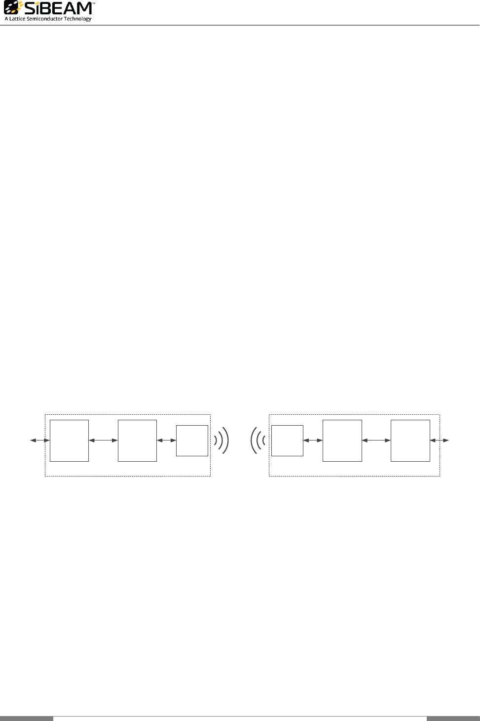
MOD65410
Baseband
Board
Network
Processor
MOD63422
RF Board
PCIe
Network Node
Network
Processor
PCIe
Network Node
IP DataIP Data
MOD65410
Baseband
Board
MOD63422
RF Board
Figure 1.1. Typical Application
MOD65412 Wireless Link Module Set
Preliminary Data Brief
4 © 2018 Lattice Semiconductor SB-DB-02006-0.80
All rights reserved. CONFIDENTIAL
2. System Description
2.1. Block Diagram
The MOD65412 Wireless Link Module Set block diagram is presented below (Figure 2.1).
SB6541
Power Supply
50-pin Connector
50-pin Connector
SiI6342
P.S.
1.8V 1.1V
1.0V
3.3Vaux
PET0p/n
PER0p/n
REFCLK+/-
W_DISABLE1#
LED_WWAN#
PERST#
54MHz
HSBUS RF I/Q
RF I/QHSBUS PCLK
PCLK
3.3V
Flash
SPI
PCIe Mini-Card
Edge Connector
Baseband Board
RF Board
50-pin Connector
50-pin Connector
GND
GND
GND
RST#
FPC Cable
TX0-TX11RX0-RX11
Antennas on PCB
Figure 2.1. Wireless Link Module Set Block Diagram
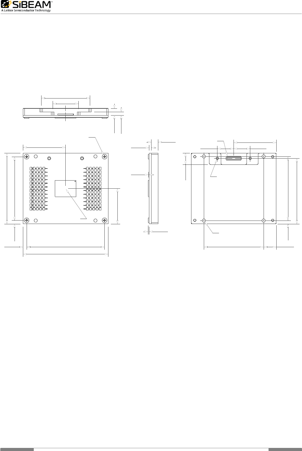
2.2. Baseband Board Dimensions
The MOD65410 baseband board is a PCI Express Half-Mini Card. Refer to the PCI Express® Mini Card Electromechanical
Specification, Revision 2.0, for the bare PCB dimensions. The PCI Express system connectoris card edge is 0.8 mm pitch,
52 pins.
The baseband board is 30 mm × 26.8 mm × 4.6 mm, with an EMI enclosure on the top side and without the FPC cable
attached. The board is 30 mm × 26.8 mm × 5.1 mm with a standard height FPC connector attached.
The two mounting screws are M2: ISO 7045:2011 M2×0.4 Pan head screws with type H or Z crosscut drive or M2.5: ISO
7045:2011 M2.5×0.45 Pan head screws with type H or Z crosscut drive.
10.45
28.60
23.90
3.85
4.50 15.60
CN1
Pin 1
2.40 MAX
1.00 0.10`
1.20 MAX
8.25
24.20
30.00 + 0
-0.30
26.80 + 0
-0.30
2.152x REF
R0.80
2xMAX
3.202x MIN
4.00 0.10`
1.50 0.10`
n2.60
2x
23.90
Figure 2.2. Baseband Board Mechanical Dimensions
MOD65412 Wireless Link Module Set
Preliminary Data Brief
SB-DB-02006-0.80 © 2018 Lattice Semiconductor 5
All rights reserved. CONFIDENTIAL
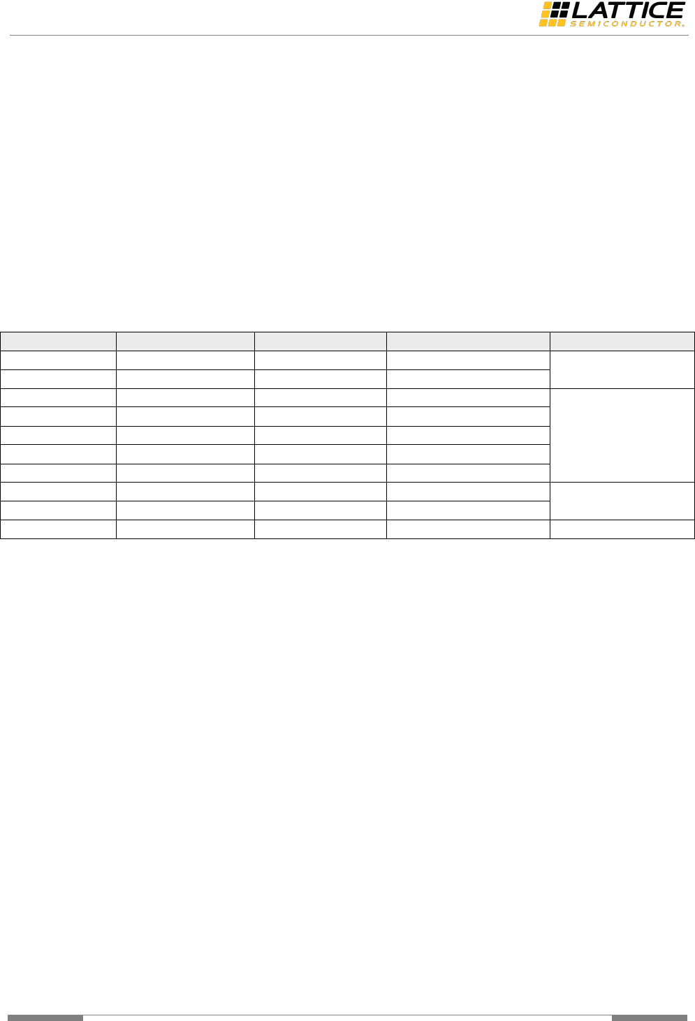
2.3. RF Board Dimensions
The MOD63422 RF board is 62.6 mm × 51.6 mm × 7.4 mm. The PCB bottom side is covered by a combination EMI
shield/heat sink block. There are two M2×0.4 threaded screw holes in the heat sink for attaching a cable retention
plate, if needed to prevent the FPC cable from working loose due to shock and vibration. There are four holes in the
PCB and heat sink that can be used to mount the module to the system assembly. These holes are 2.4 mm in diameter.
M2 wafer head screws are recommended for mounting the module to the system.
The four mounting screws are M2: ISO 7045:2011 M2×0.4 Wafer head screws with type H or Z crosscut drive.
51.60
46.40
62.60
57.40
2.60
2.60
25.80
31.30
RX Antenna Elements
TX Antenna Elements
4x M2x0.4-5 Wafer Head Cross-drive Screws
Center of SiI6342IZU IC
5.00
1.60
0.62
0.80
9.3044.00
2.40 46.80
47.80
31.30
12.1012.10
8.30
4 x 2.40 THRUn x
2 x M2x0.4 THRUx
J1
Pin 1
2.50
5.00
36.00
19.00
q
Figure 2.3. RF Board Mechanical Dimensions
2.4. Baseband and RF Board Interconnect
The baseband and RF boards each have connectors for FPC cable.
On the baseband board
Connector type: Hirose DDF40C series
Part number: DF40C-50DS-0.4V(51)
Description: Dual row board-to-board socket, 0.4 mm pitch, 50 pins, 1.5 mm stacking height
On the RF board
Connector type: Hirose DF40C series
Part number: DF40C-50DP-0.4V(51)
Description: Dual row board-to-board plug, 0.4 mm pitch, 50 pins, 1.5 mm stack height
The FPC cable has mating connectors on each end.
Connector types: Hirose DF40C series
Part numbers:DF40C-50DP-0.4V(51) on the baseband board end
DF40C-50DS-0.4V(51) on the RF board end
For technical details of the connectors, refer to the information provided by the manufacturer at
https://www.hirose.com/product/en/products/DF40/
MOD65412 Wireless Link Module Set
Preliminary Data Brief
6 © 2018 Lattice Semiconductor SB-DB-02006-0.80
All rights reserved. CONFIDENTIAL
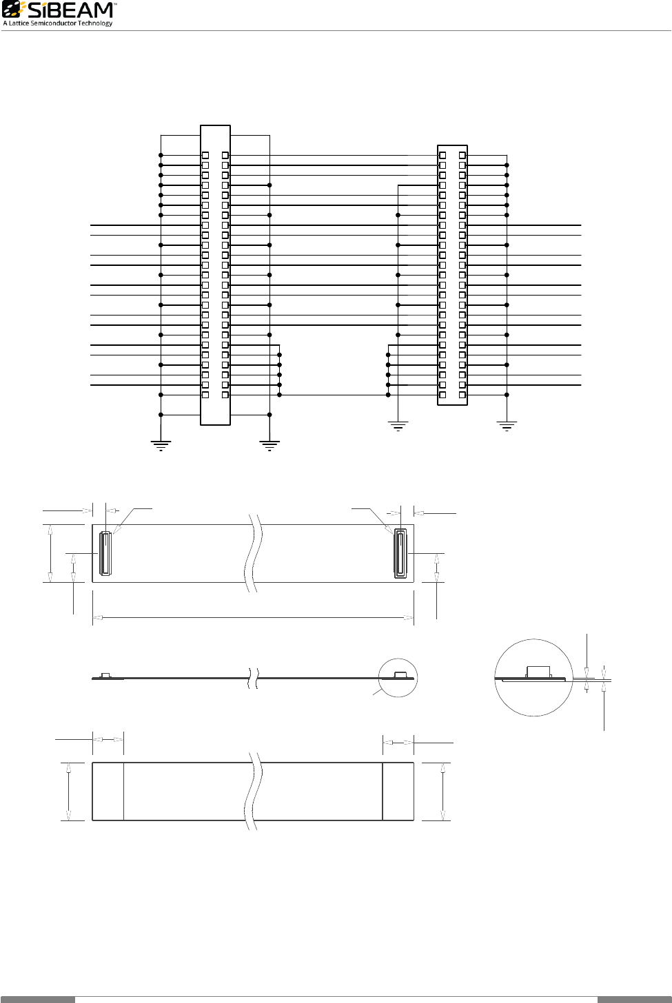
2.5. Board Interconnect Cable
MOD65412 Wireless Link Module Set uses an FPC cable to connect high speed signals between the baseband board
and the RF board.
This implementation of the FPC interconnect is 150 mm long, with board-to-board connectors at either end. The cable
is folded to connect the baseband board inside the host system to the RF board mounted on an exterior surface of the
host system. The FPC has two layers, with all signals routed on one layer and a ground plane on the second layer. The
construction of the FPC cable is shown in Table 2.1 below. The geometry used with this implementation is 165 µm
traces for single-ended 50 Ω signals and 100/100/100 µm trace/space/trace for 100 Ω differential signal pairs.
In designing a system specific FPC cable, care must be taken to match the trace lengths of the two signals in a
differential pair as closely as possible. In addition to matching pair trace lengths, the lengths of the TXI/TXQ pairs must
be matched, the lengths of the RXI/RXQ pairs must be matched, and the lengths of the HSD[0-3]/HSCS/HSCLK pairs
must be matched. The cable included with the Starter Kit matches differential pair trace lengths and group trace
lengths to <5 µm.
Table 2.1. FPC Interconnect Cable Cross Section
Circuit Layer
Thickness
Unit
Material
FPC Construction
—
12.5
µm
Polyamide
Top Coverlay
—
15
µm
Adhesive
Top
34
µm
Copper
Double-sided FPC
—
20
µm
Adhesive
—
50
µm
Polyamide
—
20
µm
Adhesive
Bottom
34
µm
Copper
—
15
µm
Adhesive
Bottom Coverlay
—
12.5
µm
Polyamide
Total thickness
213
µm
—
—
MOD65412 Wireless Link Module Set
Preliminary Data Brief
SB-DB-02006-0.80 © 2018 Lattice Semiconductor 7
All rights reserved. CONFIDENTIAL
RST_N
HSD0_N
HSD0_P
STBY
HSDOUT
RXI_N
RXI_P
TXQ_P
TXQ_N
TXI_N
TXI_P
RXQ_N
RXQ_P
PCLK_N
PCLK_P
HSD2_P
HSD2_N
HSD1_N
HSD1_P
HSD3_N
HSD3_PHSCLK_N
HSCLK_P
HSCS_P
HSCS_N
HSD0_P
HSD0_N
HSCLK_N
TXI_N
TXI_P
RXI_P
HSCLK_P
TXQ_N
TXQ_P
RXI_N
RXQ_P
RXQ_N
3V3
J1
DF40C-50DP-0.4V
HIROSE_DF40C-50DP
12 34 56 78 910 1112 1314 1516 1718 1920 2122 2324 2526 2728 2930 3132 3334 3536 3738 3940 4142 4344 4546 4748 4950
5152
5354
J2
DF40C-50DS-0.4V
HIROSE_DF40C-50DS
1 2
3 4
5 6
7 8
9 10
11 12
13 14
15 16
17 18
19 20
21 22
23 24
25 26
27 28
29 30
31 32
33 34
35 36
37 38
39 40
41 42
43 44
45 46
47 48
49 50
Baseband Module End of Cable RF Module End of Cable
Figure 2.4. FPC Interconnect Cable Schematic
A
150
7.5
3.4
7.5
15
3.4
Pin 1 Pin 1
J1
Baseband Board End J2
RF Board End
15
88
15
0.2
0.3
Detail A
Scale 2:1
Figure 2.5. FPC Interconnect Cable Mechanical Dimensions
MOD65412 Wireless Link Module Set
Preliminary Data Brief
8 © 2018 Lattice Semiconductor SB-DB-02006-0.80
All rights reserved. CONFIDENTIAL
3. Electrical Interface
This section describes the Electrical Interface between the module set and the host system. The system connector is a
52-pin card edge connector that is compliant with the PCIe Mini Card specification. Refer to the PCI Express® Mini Card
Electromechanical Specification, Revision 2.0, for complete details on the card form factor and interface signals.
3.1. Pin Out
Table 3.1. System Interface Pin Out
Name
Pin Number
Signal Type
Direction
Description
Function Group
PETn0†
31
—
I
PCI Express differential transmit
pair
System data/control
PETp0†
33
—
I
PERn0†
23
—
O
PCI Express differential receive
pair
System data/control
PERp0†
25
—
O
REFCLK-
11
—
I
PCI Express differential reference
clock (100 MHz)
System data/control
REFCLK+
13
—
I
CLKREQ#
7
LVCMOS
O
Reference clock request
System control
PERST#
22
LVCMOS
I
Functional reset to the module
System control
W_DISABLE1#
20
Open-Drain
3.3V tolerant
I
Radio operation disable signal
System control
LED_WLAN#
44
Open-Drain
3.3V tolerant
O
LED control signal to indicate
radio enabled for transmitting
System control
3.3Vaux
2, 24, 39,
41, 52
3.3 V
± 5%, 1 A
—
3.3 V source
Module power
GND
4, 9, 15, 18,
21, 26, 27,
29, 34, 35,
37, 40, 43,
50
Electrical
Ground
—
Ground
Module power
RSVD/NC
1, 3, 5, 6, 8,
10, 12, 14,
16, 17, 19,
28, 30, 32,
36, 38, 42,
44, 45, 46,
47, 48, 49,
51
N/C
—
Card edge pins not used by
module
Reserved pins
† The PET and PER differential pairs are named from the system board point of view. The PETp0 and PETn0 pins are connected to the
PCI Express transmitter differential pair on the system board and to the PCI Express receiver differential pair on the SB6541 device
on the baseband board. The PERp0 and PERn0 pins are connected to the PCI Express receiver differential pair on the system board
and to the PCI Express transmitter differential pair on the SB6541 device on the baseband board.

MOD65412 Wireless Link Module Set
Preliminary Data Brief
SB-DB-02006-0.80 © 2018 Lattice Semiconductor 9
All rights reserved. CONFIDENTIAL
3.2. Description
3.2.1. 3.3 V
The PCI Express Mini Card edge connector supplies 3.3 V power to the module set. Due to the nature of the wireless
power optimization implemented in this module set, the average power consumed by the module is much lower than
the peak power, which is transient.
Parameter
Value
Power Input VIN
3.3 V DC, 1.1 A
Max Input Voltage Ripple
±9%
Max Power
Baseband: 1.0W, RF: 2.7W
Typical Power (at MCS6)
Baseband: 0.7W, RF: 1.5W
Idle Power
Baseband: 0.6W, RF: 0.9W
3.2.2. GND
These pins provide the common power and signal ground returns for the module.
3.2.3. PCI Express x1 Lane
The PETp0/PETn0 and PERp0/PERn0 differential pairs make up a ×1 PCI Express Lane that are the primary means of
communicating with and controlling the module setMOD65412 Wireless Link Module Set. The signals are named with
respect to the host platform. The PETp0/PETn0 signals are the input pair and are connected to the receiver pins on the
SB6541 device on the baseband board. The PERp0/PERn0 signals are the output pair and are connected to the
transmitter pins on the SB6541 device through DC-blocking capacitors.
3.2.4. Reference Clock
The REFCLK+/REFCLK- differential pair is an input to the baseband board. The reference clock is a 100 MHz clock used
to assist the synchronization of the SB6541 device PCI Express interface timing circuits. The reference clock is required
by the SB6541 device for proper operation.
3.2.5. CLKREQ#
The CLKREQ# signal is an active low output from the baseband board. It is used by the baseband board to request that
the host platform supply a PCI Express reference clock. The baseband board ties this signal low through a 1 KΩ
pull-down.
3.2.6. PERST#
The PERST# signal is an input to the baseband board. It is used by the host platform to indicate the system power
source state and to force a hardware reset on the module. The host platform de-asserts (drives high) the signal when
the system power sources are stable and within tolerance specifications. The host platform asserts (drives low) the
signal when the system power is turned off or goes out of spec.
3.2.7. W_DISABLE1#
The W_DISABLE1# signal is an active low input to the baseband board. The host platform can use this signal to indicate
to the baseband processor that the radio should be disabled.
3.2.8. LED_WWAN#
The LED_WWAN# signal is an active low output from the baseband board intended to drive an LED indicator on the
host platform. It is used to indicate when the module has enabled the radio for transmission.
MOD65412 Wireless Link Module Set
Preliminary Data Brief
10 © 2018 Lattice Semiconductor SB-DB-02006-0.80
All rights reserved. CONFIDENTIAL
4. Grants and Labeling
The MOD65412 Module Set is subject to modular approval in regulatory regions. The United States of America (FCC) is
the first region that the module is certified. In order to comply with radiation exposure limit set by the FCC, the system
where the module is installed must operate at a distance of 30 cm away from any person. It is under such condition
that the system integrator can use the MOD65412 modular grant.
The MOD65412 modular grant covers three components of the module: the baseband board, the RF board, and the
FPC cable. The grant allows the system integrator to use different lengths of the FPC cable between 75 mm and
250 mm to meet specific system design requirements. The FPC cable reference design can be obtained through Lattice
Semiconductor sales representatives.
The following grants have been issued for the MOD65412 module set:
Model: MOD65412:
FCC (USA): UK2-MOD65412
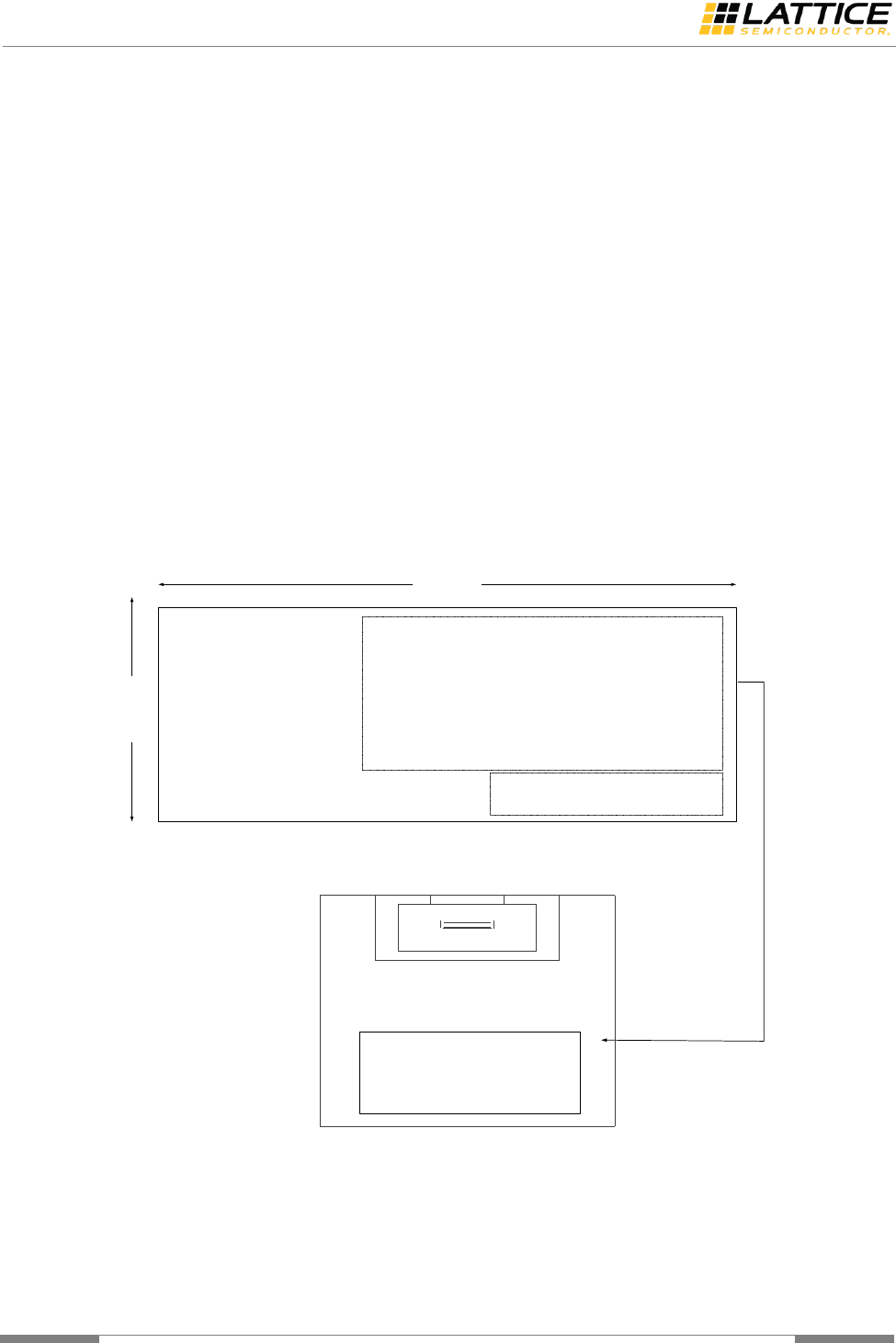
4.1. Module Label Examples
The labels attached to the model set provide identification and traceability in addition to displaying regulatory grants.
Example labels are shown below. The exact layout may differ, but all important information should be displayed clearly.
Lattice Semiconductor
Corporation
BAR CODE AREA
Made in Country
ODM or OEM marks: for example
Lot number, Product ID
15 mm
38 mm
Label Color: White
Text Color: Black
Material: adhesive and Time Resistant (Polyester)
2115 O’Nel Drive San Jose, CA
95131, USA
PN: MOD63422
OPN: MOD63422
LABEL
Figure 4.1. Example Label on MOD63422
MOD65412 Wireless Link Module Set
Preliminary Data Brief
SB-DB-02006-0.80 © 2018 Lattice Semiconductor 11
All rights reserved. CONFIDENTIAL
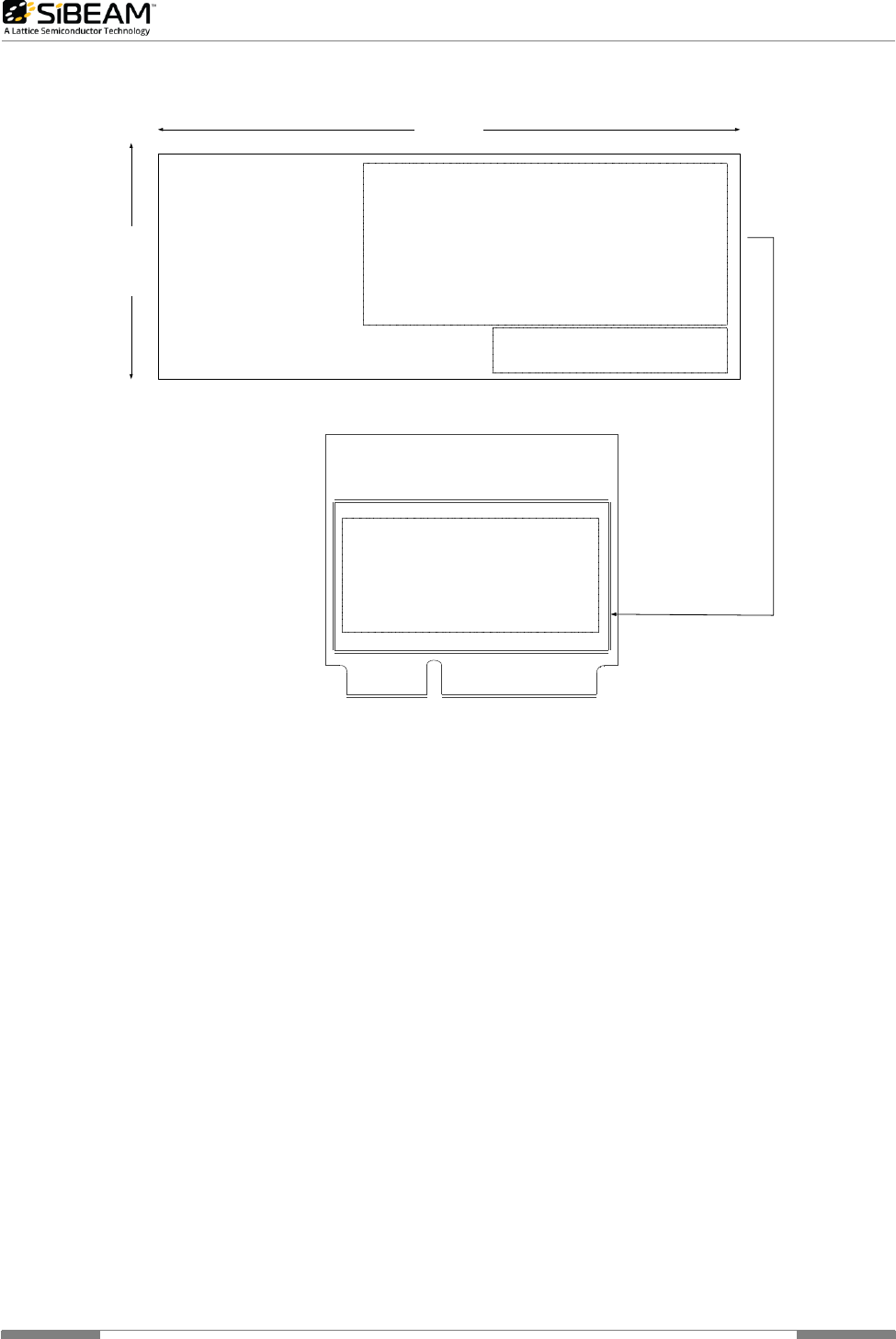
Lattice Semiconductor
Corporation
BAR CODE and MAC address Area
Made in Country
ODM or OEM marks: for example
Lot number, Product ID
14 mm
28 mm
Label Color: White
Text Color: Black
Material: adhesive and Time Resistant (Polyester)
2115 O’Nel Drive San Jose, CA
95131, USA
OPN: MOD65412
(MOD63422 + MOD65410)
PN: MOD65410
FCC ID: UK2-MOD65412
LABEL
Figure 4.2. Example Label on MOD65410

MOD65412 Wireless Link Module Set
Preliminary Data Brief
12 © 2018 Lattice Semiconductor SB-DB-02006-0.80
All rights reserved. CONFIDENTIAL
Ordering Information
Device
Ordering Part Number
Lattice GigaRay Module Set
MOD65412

MOD65412 Wireless Link Module Set
Preliminary Data Brief
SB-DB-02006-0.80 © 2018 Lattice Semiconductor 13
All rights reserved. CONFIDENTIAL
Appendix A. OEM Installation
A.1. Interference Statement
USA - Federal Communications Commission (FCC)
This equipment has been tested and found to comply with the limits for a Class B digital device, pursuant to Part 15 of
FCC Rules. These limits are designed to provide reasonable protection against harmful interference in a residential
installation. This equipment generates, uses, and can radiate radio frequency energy. If not installed and used in
accordance with the instructions, it may cause harmful interference to radio communications. However, there is no
guarantee that interference will not occur in a particular installation.
1. This device complies with Part 15 of the FCC Rules. Operation is subject to the following two conditions: (1) this
device may not cause harmful interference, and (2) this device must accept any interference received, including
interference that may cause undesired operation.
2. This product does not contain any user serviceable components. Any unauthorized product changes or
modifications will invalidate warranty and all applicable regulatory certifications and approvals.
3. Caution: Exposure to Radio Frequency Radiation: The installer of this radio equipment must place the module
inside the enclosure of a stationary system intended to operate 30 cm away from the end user body in typical
operation. This implies that this module shall not be integrated in battery operated devices, handheld devices,
wearable accessories for example.
4. The antenna(s) used for this transceiver must not be collocated or operating in conjunction with any other
antenna or transmitter within a host device, except in accordance with FCC multi-transmitter product procedures.
Other antennas shall be installed with a minimum 30 cm separation from the 60 GHz device antenna present in
this module.
5. Caution: User is cautioned that changes or modifications not expressly approved by the party responsible for
compliance could void the user's authority to operate the equipment.
6. FCC rule 15.255(a) prohibits the use of this device on aircrafts or satellites.
7. This module is intended for the OEM integrator.
Additional note to System Integrator/OEM:
The regulatory label on the final system must include the exact statement:
“Contains FCC ID: UK2-MOD65412” on the enclosure

MOD65412 Wireless Link Module Set
Preliminary Data Brief
14 © 2018 Lattice Semiconductor SB-DB-02006-0.80
All rights reserved. CONFIDENTIAL
Revision History
Revision 0.80, February 2018
First preliminary release.