Lester Electrical of Nebraska 28170 Bluetooth Low-Energy Module for Digital Communication User Manual Focus Lab prototype software interface
Lester Electrical of Nebraska Inc Bluetooth Low-Energy Module for Digital Communication Focus Lab prototype software interface
Users Manual Rev 2
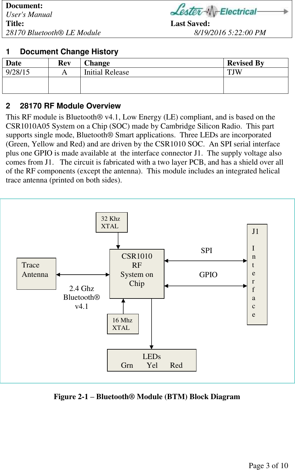
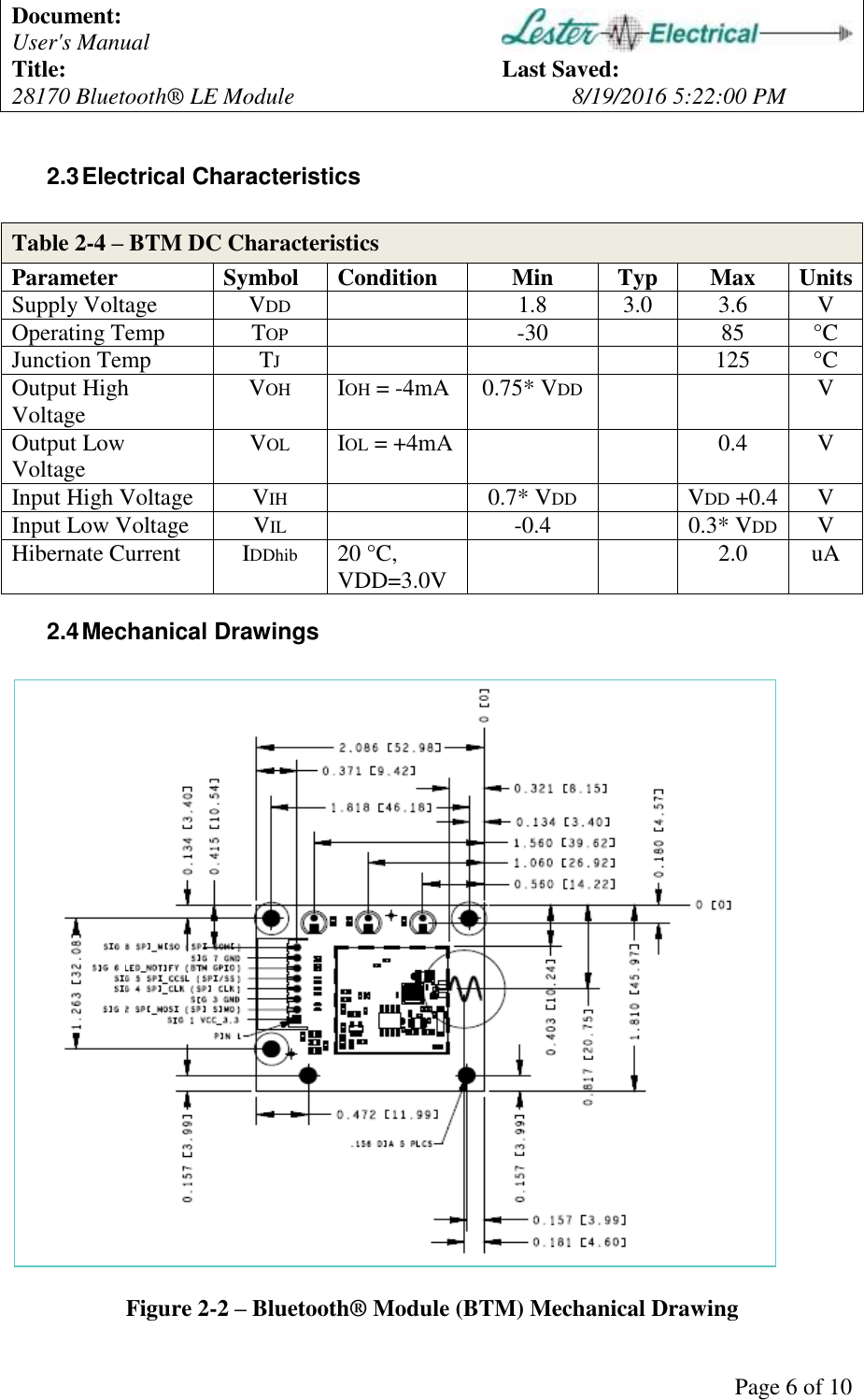
![Document: User's Manual Title: Last Saved: 28170 Bluetooth® LE Module 8/19/2016 5:22:00 PM Page 4 of 10 2.1 Specifications Table 2-1 – BTM Specifications General Frequency ISM 2.4 Ghz Number of Channels (3 used for advertising) 40 Spreading Method Frequency hopping, pseudo-random, adaptive Modulation GFSK Bluetooth® Smart V4.1 Antenna Trace, Helix 2 sided Dimensions 2.086[52.98] x 1.810[45.97] Inches[mm] x 0.492[12.50] Operating Temperature -30 to 85 °C Storage Temperature -40 to 85 °C Power Requirements Supply Voltage (Switching Regulator Input) 1.8 to 3.6 V Transmit Current 1 (TX level = 4, 0 dBm) 18mA peak at 3.0V Receive Current 1 20mA peak at 3.0V Idle Current 1 1 mA at 3.0V Available I/O SPI Serial Port 4, including chip select Additional GPIO 1 Performance Transmit Output Power, Conducted -16 to +9 dBm Receiver Sensitivity -93 dBm RF Data Rate 1 Mbps Agency Approvals FCC Parts 15.209, 15.247 FCC ID: OBH-28170 Industry Canada (IC) IC: nnnnn-28170 1 Currents listed are with all LEDs off. 40mA is the maximum expected peak current, at max transit power with all LEDs on.](https://usermanual.wiki/Lester-Electrical-of-Nebraska/28170/User-Guide-3138137-Page-4.png)
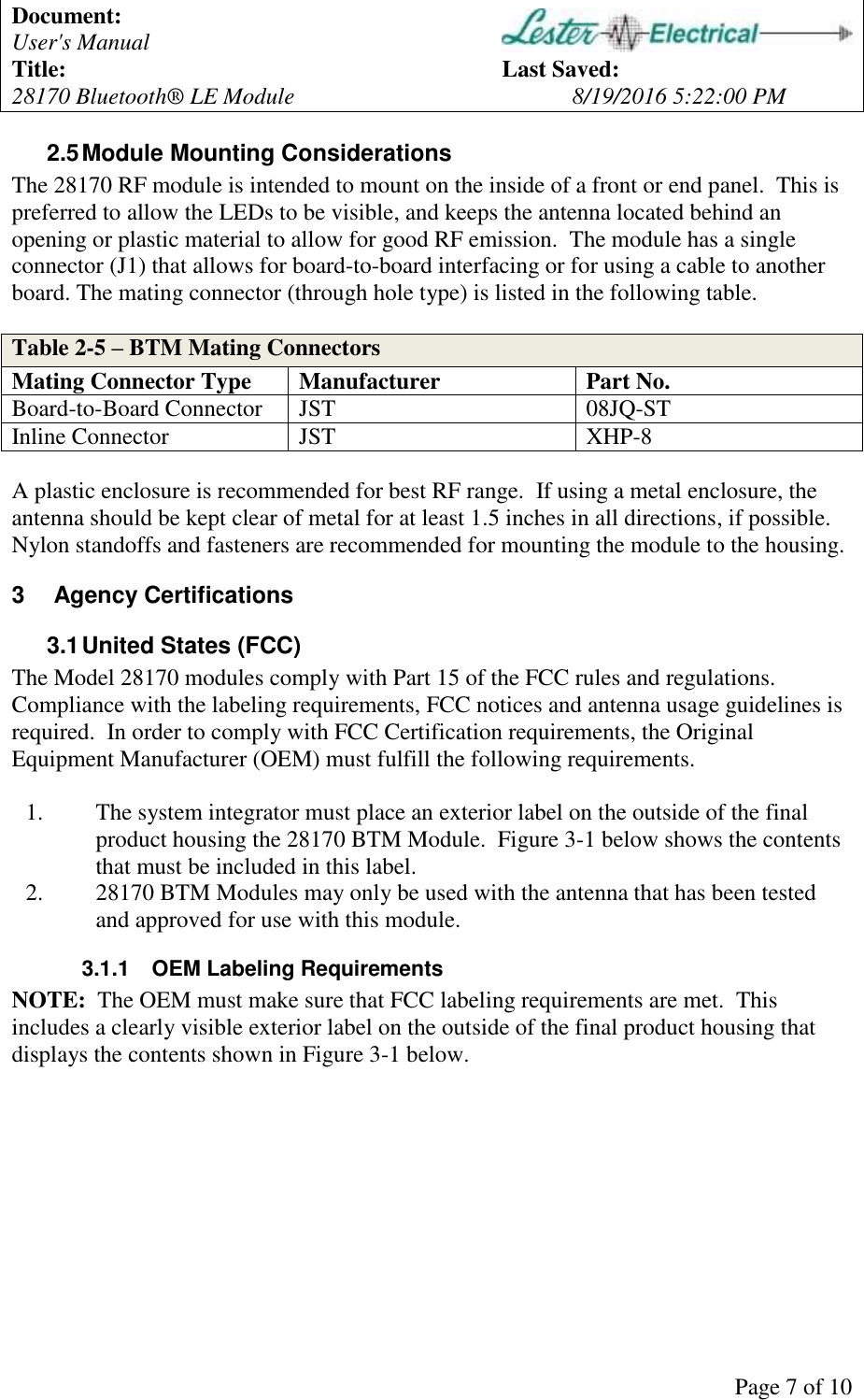
![Document: User's Manual Title: Last Saved: 28170 Bluetooth® LE Module 8/19/2016 5:22:00 PM Page 5 of 10 2.2 Module Pin-Out, Signal Descriptions Table 2-2 – J1 Connector, Interface Description J1 Pin Signal Name Description Direction 1 VCC_3.3 Positive Power Supply Voltage, Normally 3.3V Power 2 SPI_MOSI (SPI SIMO) SPI Bus, Master Output / Slave Input Input/Output 3 GND Ground Pin Power 4 SPI_CLK (SPI CLK) SPI Bus, Master Clock Output Input/Output 5 SPI_CCSL (SPI /SS) SPI Bus, Chip Select Active Low (/Slave Select) Input/Output 6 LED_Notify (BTM GPIO) General Purpose GPIO Input/Output 7 GND Ground Pin Power 8 SPI_MISO (SPI SOMI) SPI Bus, Master Input / Slave Output Input/Output Table 2-3 – BTM LED Port Pins CSR1010 Port I/O Signal Name Description Direction PIO[0] Grn_LED Green LED, Active Low - On 1 Output PIO[1] Yel_LED Yellow LED, Active Low - On 1 Output PIO[6] Red_LED Red LED, Active Low - On 2 Output 1 The Green and Yellow LEDs are shared with the CSR UART debug Pins on PIO[0] and PIO[1]. Avoid I/O contention by not using the debug UART. 2 The Red LED is shared with the CSR Chip Select on PIO[6]. A buffer with open-drain output is recommended (for the programming I/F) to avoid I/O contention.](https://usermanual.wiki/Lester-Electrical-of-Nebraska/28170/User-Guide-3138137-Page-5.png)