Lg Gsa 4165B Users Manual
GSA-4165B GSA-4165 Manual de Servicio
GSA-4165B to the manual 51c64404-3991-4947-9402-0817f9056704
2015-01-26
: Lg Lg-Gsa-4165B-Users-Manual-228490 lg-gsa-4165b-users-manual-228490 lg pdf
Open the PDF directly: View PDF ![]() .
.
Page Count: 86

Super Multi DVD Drive
S E RVICE MANUAL
MODEL: GSA-4165B/
G S A - 4 1 6 7 B /
G S A - 4 1 6 8 B
P/NO : 3828HS1047G
August 2005
Printed in Korea
MODEL : GSA-4165B/GSA-4167B/GSA-4168B

TABLE OF CONTENTS
INTRODUCTION .......................................................................................................................................................................3
FEATURES............................................................................................................................................................................3~5
SPECIFICATIONS.................................................................................................................................................................6~9
LOCATION OF CUSTOMER CONTROLS .......................................................................................................................10~11
DISASSEMBLY.................................................................................................................................................................12~13
1. CABINET and CIRCUIT BOARD DISASSEMBLY ..........................................................................................................12
1-1. Bottom Chassis..........................................................................................................................................................12
1-2. Front Bezel Assy........................................................................................................................................................12
1-3. Cabinet and Main Circuit Board .................................................................................................................................12
2. MECHANISM ASSY DISASSEMBLY..............................................................................................................................12
2-1. Pick-up Unit................................................................................................................................................................12
2-2. Pick-up ......................................................................................................................................................................13
EXPLODED VIEW.............................................................................................................................................................14~15
MECHANICAL REPLACEMENT PARTS LIST ................................................................................................................16~18
GLOSSARY.............................................................................................................................................................................19
THE DIFFERENCES OF CD-R/CD-RW DISCS AND GENERAL CD-ROM.....................................................................20~26
1. Recording Layer ..............................................................................................................................................................20
2. Disc Specification ............................................................................................................................................................20
3. Disc Materials..................................................................................................................................................................21
4. Reading Process of Optical Disc.....................................................................................................................................22
5. Writing Process of CD-R Disc .........................................................................................................................................23
6. Writing Process of CD-RW Disc......................................................................................................................................23
7. Organization of the PCA, PMA and Lead-in Area ...........................................................................................................24
8. Function of PCA and PMA area ......................................................................................................................................25
9. OPC and ROPC ..............................................................................................................................................................25
10. Writing Process of DISC................................................................................................................................................26
THE DIFFERENCES OF DVD-R/RW, DVD+R/RW DISCS AND DVD-ROM....................................................................27~35
1. Recording Layer ..............................................................................................................................................................27
2. Disc Specification ............................................................................................................................................................28
3. Disc Materials..................................................................................................................................................................28
4. Writing Pulse Waveform of DVD+R.................................................................................................................................31
5. Writing Pulse Waveform DVD+RW .................................................................................................................................33
6. Organization of Inner Drive Area, Outer Drive Area, Lead-in Zone and Lead-out Zone .................................................34
LightScribe MEDIA...........................................................................................................................................................36~39
1. LightScribe Media............................................................................................................................................................36
2. Hardware Block Diagram of LightScribe Label Printing...................................................................................................37
3. MD Assy For LightScribe.................................................................................................................................................38
4. Optical Encoder Assy ......................................................................................................................................................39
DVD & CD DATA PROCESSING......................................................................................................................................40~43
1. Data Processing Flow......................................................................................................................................................40
2. Copy Protection and Regional Code Management Block ...............................................................................................41
3. About Prevention the DVD-ROM from to be copy...........................................................................................................42
4. About the DVD-ROM Regional Code ..............................................................................................................................43
INTERNAL STRUCTURE OF THE PICK-UP....................................................................................................................44~46
1. Block Diagram of the Pick-up(HOP-7632TS) ..................................................................................................................44
2. Pick up Pin Assignment...................................................................................................................................................45
3. Signal detection of the P/U..............................................................................................................................................46
DESCRIPTION OF CIRCUIT.............................................................................................................................................47~53
1. ALPC Circuit....................................................................................................................................................................47
2. Focus Circuit....................................................................................................................................................................49
3. Tracking & Sled Circuit....................................................................................................................................................50
4. Spindle Circuit .................................................................................................................................................................53
MAJOR IC INTERNAL BLOCK DIAGRAM AND PIN DESCRIPTION.............................................................................55~72
TROUBLESHOOTING GUIDE..........................................................................................................................................73~90
BLOCK DIAGRAM..................................................................................................................................................................91
PRINTED CIRCUIT BOARD DIAGRAM ...........................................................................................................................92~96
ELECTRICAL REPLACEMENT PARTS LIST........................................................................................................................97
CAUTION - INVISIBLE LASER RADIATION WHEN OPEN AVOID EXPOSURE TO BEAM.

3
This service manual provides a variety of service
information.
It contains the mechanical structure of the Super
Multi DVD Drive and the electronic circuits in
schematic form. This Super Multi DVD Drive was
manufactured and assembled under our strict quality
control standards and meets or exceeds industry
specifications and standards.
This Super Multi DVD drive is an internal drive unit
designed for use with IBM PC, HP Vectra, or
compatible computer. It can write as much as 700
Mbytes of digital data into CD-R/RW disc, and can
read as much as 700 Mbytes of digital data stored in
a CD-ROM/R/RW disc.
It can write as much as 4.7Gbytes of digital data into
DVD-R/RW/RAM/+R/+RW disc, and can read as
much as 4.7Gbytes of digital data stored in a
DVD-ROM/R/RW/RAM/+R/+RW disc.
It can write as much as 8.5Gbytes of digital data into
DVD+R DL/DVD-R DL disc, and can read as much
as 8.5Gbytes of digital data stored in a DVD-ROM
DL/+R DL/-R DL disc.
This Super Multi DVD Drive can easily meet the
upcoming MPC level 3 specification, and its
Enhanced Intelligent Device Electronics (E-IDE) and
ATAPI interface allows Plug and play integration in
the majority of today’s PCs without the need of an
additional interface card.
INTRODUCTION
1. Support feature and writable disc
*) Indicated write-in speed is a value at the time of the fastest operation.
G*A-4165B
GSA GMA GWA GRA GCA GDA
Light Scribe x x x x x x
CD-R 48x write 48x write 48x write 48x write 48x write read only
CD-RW 32x write 32x write 32x write 32x write 32x write read only
DVD-R 16x write 16x write 16x write read only 16x write 16x write
DVD-RW 4x or 6x write 4x or 6x write 4x or 6x write read only 4x or 6x write 4x or 6x write
DVD-R DL 4x write 4x write 4x write read only 4x write 4x write
DVD+R 16x write read only 16x write 16x write read only read only
DVD+RW 8x write read only 8x write 8x write read only read only
DVD+R DL 4x or 6x write read only 4x or 6x write 4x or 6x write read only read only
DVD-RAM 5x write 5x write read only read only read only 5x write
G*A-4167B
GSA GMA GWA GRA GCA GDA
Light Scribe xxx xxx
CD-R 48x write 48x write 48x write 48x write 48x write read only
CD-RW 32x write 32x write 32x write 32x write 32x write read only
DVD-R 16x write 16x write 16x write read only 16x write 16x write
DVD-RW 6x write 6x write 6x write read only 6x write 6x write
DVD-R DL 4x write 4x write 4x write read only 4x write 4x write
DVD+R 16x write read only 16x write 16x write read only read only
DVD+RW 8x write read only 8x write 8x write read only read only
DVD+R DL 6x write read only 6x write 6x write read only read only
DVD-RAM 5x write 5x write read only read only read only 5x write
G*A-4168B
GSA GMA GWA GRA GCA GDA
Light Scribe O O O O O O
CD-R 48x write 48x write 48x write 48x write 48x write read only
CD-RW 32x write 32x write 32x write 32x write 32x write read only
DVD-R 16x write 16x write 16x write read only 16x write 16x write
DVD-RW 6x write 6x write 6x write read only 6x write 6x write
DVD-R DL 4x write 4x write 4x write read only 4x write 4x write
DVD+R 16x write read only 16x write 16x write read only read only
DVD+RW 8x write read only 8x write 8x write read only read only
DVD+R DL 6x write read only 6x write 6x write read only read only
DVD-RAM 5x write 5x write read only read only read only 5x write

4
FEATURES
1 General
1) Enhanced IDE (ATAPI) interface.
2) Internal Half-height Drive.
3) CD-R/RW, DVD-R/-R DL(Dual Layer)/-RW/RAM/+R/+R DL(Double Layer)/+RW read and write
compatible CD Family and DVD-ROM read compatible.
4) Buffer Under-run prevention function embedded.
5) 2MB buffer memory.
6) Power loading and power eject of a disc. Bare media loading.
7) MTBF : 100,000 POH
8) Vertical and Horizontal installable.
2. Supported disc formats
1) Reads data in each DVD-ROM, DVD-R(Ver. 2.0 for Authoring) and DVD-RAM(Ver.1.0)
2) Reads and writes in each DVD-R(Ver. 2.0 for General), DVD-R DL(Dual Layer), DVD-RW, DVD-
RAM(Ver.2.2), DVD+R, DVD+R DL(Double Layer) and DVD+RW
3) Reads data in each CD-ROM, CD-ROM XA, CD-I, Video CD, CD-Extra and CD-Text
4) Reads data in Photo CD (Single and Multi session)
5) Reads standard CD-DA
6) Support to read Super Audio CD(Compatible layer in Hybrid type)
7) Reads and writes CD-R discs conforming to “Orange Book Part 2”
8) Reads and writes CD-RW discs conforming to “Orange Book Part 3”
9) Reads DVD-RAM with CPRM and DVD-RW with CPRM
3. Supported write method
1) DVD-R:..................Disc at Once and Incremental Recording
2) DVD-R DL .............Disc at Once, incremental Recording and Layer jump recording
3) DVD-RW:...............Disc at Once, Incremental Recording and Restricted Overwrite
4) DVD-RAM:.............Random Write
5) DVD+R:.................Sequential Recording
6) DVD+R DL: ...........Sequential Recording
7) DVD+RW:..............Random Write
8) CD-R/RW: .............Disc at Once, Session at Once, Track at Once and Packet Write

4. Performance
1) Average access time: DVD-ROM 145 ms
(1/3 stroke) CD-ROM 125 ms
2) Write speed: DVD-R 2x, 4x CLV, 8x ZCLV, 16x PCAV
DVD-R DL 2x, 4x CLV
DVD-RW 1x, 2x, 4x, 6x CLV
DVD-RAM 2x, 3x ZCLV (Ver.2.2), 3x-5x PCAV(Ver.2.2)
DVD+R 2.4x, 4x CLV, 8x ZCLV, 12x, 16x PCAV
DVD+R DL 2.4x, 4x, 6x CLV
DVD+RW 2.4x, 4x CLV, 8x ZCLV
CD-R 4x, 8x, 16x CLV, 24x, 32x, 40x, 48x ZCLV
CD-RW 4x, 10x, 16x CLV, 24x, 32x ZCLV
(High Speed: 10x, Ultra Speed: 16x, 24x, 32x)
3) Read speed: DVD-R/RW/ROM/ROM-Dual layer 10x / 8x / 16x / 12x max.
DVD-R DL 8x max.
DVD-RAM (Ver.1.0/2.2) 2x / 2x, 3x ZCLV, 3x-5x PCAV
DVD-Video(CSS Compliant Disc) 8x max. (Single/Dual layer)
DVD+R/+RW 10x / 8x max.
DVD+R DL 8x max.
CD-R/RW/ROM 48x/40x/48x max.
CD-DA (DAE) 40x max.
80mm CD 16x max.
4) Sustained Transfer rate: DVD-ROM 22.16 Mbytes/s (16x) max.
CD-ROM 7,200 kB/s (48x) max.
5) Burst Transfer rate: Ultra DMA Mode2
Multi word DMA Mode2, PIO Mode 4
6) Multimedia MPC-3 compliant
5. Audio
1) 16 bit digital data output through ATA interface
2) Software Volume Control
3) Equipped with audio line output for audio CD playback
*Definition
Transfer Rate: .........1x (DVD) = 1.385 Mbytes/s..........1x (CD) = 150 kB/s
Mbytes/s = 106bytes/s, ................kB/s = 210 bytes/s
Capacity: .................MB = 220 bytes,.............................kB = 210 bytes
5

6
SPECIFICATIONS
1. SYSTEM REQUIREMENTS
-CPU: IBM Compatible Pentium 4 2.4GHz (or faster)
(For High speed, 2.4GHz or faster recommended.)
-128MB Memory or greater
2. SUPPORTING OPERATING SYSTEM
2.1 Applicable disc formats
DVD ............................DVD-ROM: 4.7GB (Single Layer)
8.5GB (Dual Layer)
DVD-R DL: 8.5GB
DVD-R: 4.7GB (Ver.2.0 for Authoring : read only)
4.7GB (Ver.2.0 for General: read & write)
DVD-RW: 4.7GB (Ver.1.2)
DVD-RAM: 2.6GB/side (Ver.1.0)
1.46GB/side, 4.7GB/side (Ver.2.2)
DVD+R: 4.7GB
DVD+R DL: 8.5GB
DVD+RW: 4.7GB
CD...............................CD-ROM Mode-1 data disc
CD-ROM Mode-2 data disc
CD-ROM XA, CD-I, Photo-CD Multi-Session, Video CD
CD-Audio Disc
Mixed mode CD-ROM disc (data and audio)
CD-Extra
CD-Text
CD-R (Conforming to “Orange Book Part2”: read & write)
CD-RW (Conforming to “Orange Book Part3”: read & write)
2.2 Writing method
(1) DVD-R/RW...........................Disc at Once
Incremental Recording
Restricted Overwrite (DVD-RW only)
(2) DVD-R DL ............................Disc at Once
Incremental Recording
Layer jump Recording
(3) DVD-RAM/+RW ...................Random Write
(4) DVD+R.................................Sequential Recording
(5) DVD+R DL ...........................Sequential Recording
(6) CD-R/RW .............................Disc at Once (DAO)
Session at Once (SAO)
Track at Once (TAO)
Packet Write
2.3 Disc diameter..............................................120mm
80mm (Horizontal only)
* Operating System
Windows Millennium Edition (Me)
Window 2000 Professional
Window XP Home Edition, Professional
* Recording tool
(1) Nero(Ahead)
(2) In CD(Ahead)
(3) Power Producer Gold (Cyber Link)

7
2.4 Data capacity
• User Data/Block DVD-ROM/R/RW/RAM/+R/+RW ......2,048 bytes/block
CD (Yellow Book) ..........................................2,048 bytes/block(Mode 1 & Mode 2 Form 1)
2,336 bytes/block (Mode 2)
2,328 bytes/block (Mode 2 Form 2)
2,352 bytes/block (CD-DA)
2.5 RPC (Regional Playback Control) Phase2, No Region
3. DRIVE PERFORMANCE
3.1 Host interface ..................................................................X3T13 ATA/ATAPI5/1321D
INF-8090i Rev.5.3
3.2 Read/Write & Rotational speed
<Write> DVD-R...............................................................2x, 4x(CLV), 8x(ZCLV), 16x(PCAV)
DVD-R DL .........................................................2x, 4x(CLV)
DVD-RW............................................................1x, 2x, 4x, 6x(CLV)
DVD-RAM ...............................Ver. 2.2.............2x, 3x(ZCLV), 3x-5x(PCAV)
DVD+R ..............................................................2.4x, 4x(CLV), 8x, 12x, 16x(PCAV)
DVD+R DL ........................................................2.4x, 4x, 6x(CLV)
DVD+RW...........................................................2.4x, 4x(CLV), 8x(ZCLV)
CD-R .................................................................4x, 8x, 16x(CLV), 24x, 32x, 40x, 48x(ZCLV)
CD-RW..............................................................4x, 10x,16x(CLV), 24x, 32x (ZCLV)
(High Speed: 10x, Ultra Speed: 16x, 24x, 32x)
<Read> DVD-ROM...............................Single layer.......6.7x - 16x (CAV), Approx. 9,420 r/min
................................................Dual layer .........5.0x - 12x (CAV), Approx. 7,770 r/min
DVD-R DL...............................8.5GB ...............3.3x - 8x (CAV), Approx 5,180r/min
DVD-Video (CSS) .............................................3.3x - 8x (CAV), Approx. 5,180 r/min
DVD-R.....................................4.7GB ...............4.2x - 10x (CAV), Approx. 5,890 r/min
DVD-RW .................................4.7GB ...............3.3x - 8x (CAV), Approx. 4,720 r/min
DVD-RAM ...............................Ver. 1.0/ 2.2......2x/ 2x, 3x (ZCLV)* 3x-5x (PCAV)*
DVD+R....................................4.7GB ...............4.2x - 10x (CAV), Approx. 5,890 r/min
DVD+R DL ..............................8.5GB ...............3.3x - 8x (CAV), Approx. 5,180 r/min
DVD+RW ................................4.7GB ...............3.3x - 8x (CAV), Approx. 4,720 r/min
CD-R/ROM, CD-I / Video........(1.2m/s) ............20x - 48x (CAV), Approx. 9,540 r/min
CD-RW ...................................(1.2m/s) ...........16.7x - 40x (CAV), Approx. 8,100 r/min
CD-DA (DAE)..........................(1.2m/s) ...........16.7x - 40x (CAV), Approx. 8,100 r/min
CD-DA (Audio out)..................(1.2m/s) ...........4.0x - 10x (CAV), Approx. 2,030 r/min
* Rotational speed (CLV, ZCLV)
DVD-R/RW/ROM, +R/RW ...............................1x: Approx. 1,390(Inside) - 580 r/min(Outside)
DVD-RAM................................Ver. 1.0 ...........1x: Approx. 2,390(Inside) - 1,010 r/min(Outside)
Ver. 2.2 ...........2x: Approx. 3,250(Inside) - 1,380 r/min(Outside)
CD-R/RW/ROM ...............................................1x: Approx. 500(Inside) - 210 r/min(Outside)

3.3 Data transfer rate
3.3.1 Sustained transfer rate
<Write> DVD-R.........................2.77, 5.54, 5.44-11.08 Mbytes/s..................................2x, 4xCLV, 8x ZCLV
9.14-22.16 Mbytes/s....................................................................16x PCAV
DVD-R DL ...................2.77, 5.54 Mbytes/s....................................................................2x, 4x CLV
DVD-RW ...............1.385, 2.77, 5.54, 8.31 Mbytes/s ...................................1x, 2x, 4x, 6x CLV
DVD-RAM (Ver.2.2): ...2.77, 4.15, 4.15-6.925 Mbytes/s (w/o Verify) .......2x, 3x ZCLV, 3-5x PCAV
DVD+R........................3.32, 5.54, 8.31-11.08 Mbytes/s..............................2.4x, 4x CLV, 8x ZCLV
8.31-16.62, 9.14-22.16 Mbytes/s ..............................12x ZCLV, 16x PCAV
DVD+R DL ..................3.32, 5.54, 8.31 Mbytes/s ..................................................2.4x, 4x, 6x CLV
DVD+RW.....................3.32, 5.54, 8.31-11.08 Mbytes/s .............................2.4x, 4x CLV, 8x ZCAV
CD-R ...........................
600, 1,200, 2,400, 2,400-3,600, 2,400-4,800, 2,400-6,000, 2,400-7,200 kB/s (Mode-1)
..........................................4x, 8x, 16x CLV 24x, 32x, 40x, 48x ZCLV
CD-RW........................600, 1500, 2,400, 2,400- 3,600, 2,400-4,800 kB/s (Mode-1)
..........................................4x, 10x, 16x CLV, 24x, 32x ZCLV
<Read> DVD-ROM ...................Single layer ....9.28 - 22.16 Mbytes/s ...........................................16x max.
....................................Dual layer.......6.86 - 16.62 Mbytes/s ...........................................12x max.
DVD-R ................................................5.73 - 13.85 Mbytes/s ............................................10x max.
DVD-R DL...........................................4.58 - 11.08 Mbytes/s ..............................................8x max.
DVD-RW.............................................4.58 - 11.08 Mbytes/s .............................................8x max.
DVD-RAM ...................Ver. 1.0 ..........2.77 Mbytes/s.........................................................2x ZCLV
....................................Ver. 2.2 ..........2.77, 4.155,4.155-6.93 Mbytes/s ..2x, 3x ZCLV, 3-5x PCAV
DVD+R ...............................................5.73 - 13.85 Mbytes/s ............................................10x max.
DVD+R DL..........................................4.58 - 11.08 Mbytes/s ..............................................8x max.
DVD+RW............................................4.58 - 11.08 Mbytes/s .............................................8x max.
CD-R/ROM .........................................3,000 - 7,200 kB/s..................................................48x max.
CD-RW........................ ......................2,500 - 6,000 kB/s..................................................40x max.
CD-DA (DAE)......................................2,500 - 6,000 kB/s..................................................40x max.
3.3.2 Burst transfer rate
Ultra DMA Mode 2 ..............................33.3 Mbytes/s max.
Multiword DMA Mode 2 ......................16.6 Mbytes/s max.
PIO Mode 4 ........................................16.6 Mbytes/s max.
3.4 Access time (1/3 stroke)
DVD-ROM...........................................145 ms Typ.*(Note 1)
DVD-RAM (Ver.2.2)............................165 ms Typ.
CD-ROM.............................................125ms Typ. (Note 1)
Note :
1) Average random access time is the typcal value of more than 50 times including latency and error correction time.
Test Disc : DVD : ALMEDIO TDV-520 / TDR-820
CD : ALMEDIO TCDR-701 / HITACHI HCD-1
*) Typical value defines a measured value in normal temperature (20 deg.C.) and horizontal position.
3.5 Data error rate (Measured with 5 retries maximum)
DVD-R/RW/ROM/RAM ..................................<10-12
DVD+R/+RW..................................................<10-12
CD-R/RW/ROM..............................................<10-12 (Mode-1)
<10-9 (Mode-2)
Condition : It is assumed that the worst case raw error rate of the disc is 10-3
3.6 Data buffer capacity .......................................................2 Mbytes
8

9
4. Quality and Reliability
4.1 MTBF..................................................100,000 Power On Hours(Consecutive/Cumulative POH)
Assumption : ..........................Used in a normall office environment at room temperature.
-POH per year.........................3,000
-ON/OFF cycles per year........600
-Operating duty cycle..............20% of power on time (Seek: 5% of operating time)
4.2 Tray cycle test...................................30,000 times
No degeneration in the mechanical part after test
4.3 Actuator mechanism........................1,000,000 full stroke seek
4.4 MTTR (Mean Time To Repair) ...........0.5 h
4.5 Component life .................................5 years or 2,000 h of Laser radiating time
Assumption : ..........................Used in a normall office environment.
5. POWER REQUIREMENTS
5.1 Source voltage
+5V +5% tolerance, less than 100 mVp-p Ripple voltage
+12V +10% tolerance, less than 100 mVp-p Ripple voltage
5.2 Current
Idle (Hold track state)..............+5V DC .................0.9A typ. .........< 1.0 A max.
+12V DC ...............0.5A typ...........< 1.0 A max.
Write (Active) ..........................+5V DC .................1.3A typ. .........< 1.5 A max.
+12V DC................0.9A typ. .........< 1.5 A max.
Read (Active)..........................+5V DC .................1.0A typ. .........< 1.5 A max.
+12V DC................0.9A typ. .........< 1.5 A max.
Seek (Acess) ..........................+5V DC .................1.0A typ. .........< 1.5 A max.
+12V DC ...............1.2A typ. .........< 2.0 A max.
5.3 Standby
Sleep mode (No disc) .............1.1 W typ. 1.3 W max.
6. AUDIO PERFORMANCE
Output Level (1kHz, 0dB)........................................................0.7 Vrms typical
Frequency Response ..............................................................+/-3dB (20 to 20,000Hz)
Signal to Noise Ratio...............................................................80 dB min. with IHF A and LPF 20 kHz
THD (1kHz, 0dB).....................................................................0.10% max. with LPF 20 kHz
Channel separation(10kHz).....................................................65 dB min.
Condition: ................................................................................Load inpedance : 10 kohms
7. Acoustic noise
Less than 50dB, A scale, at 0.5 m away from the drive
Note : 1. Disc : Less than imbalance 0.3 x 10⁻⁴ Nm
2. Installation : Horizontal
3. Ambient temperature : Normal temperature
4. Except loading, unloading and seek
8. Dimensions
External dimensions (W x H xD) 146 x 41.3 x 165mm(without Bezel)
Front bezel (WxHxD) 148 x 42 x 5 mm
9. Mass .................................................Approx. 0.77+/-0.03 kg
* Which is not provided with Circuit Diagram of this model. Please Contact the friendly staff of LG
Service Care at: Website http: //www.LGEservice.com
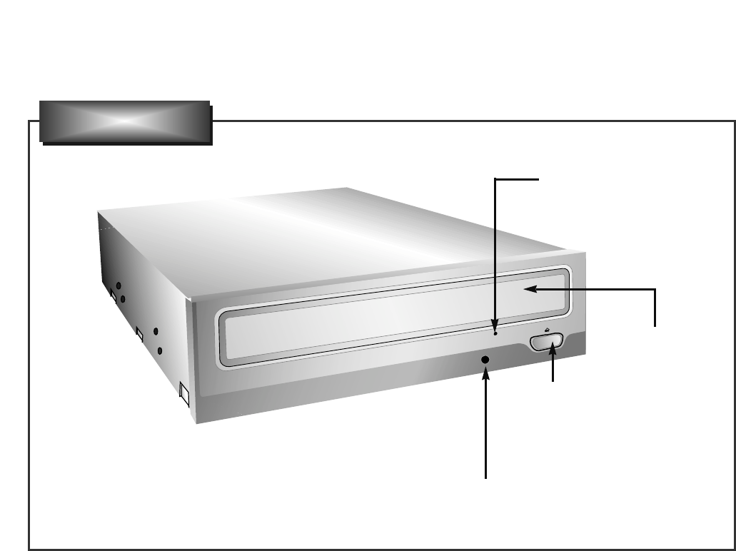
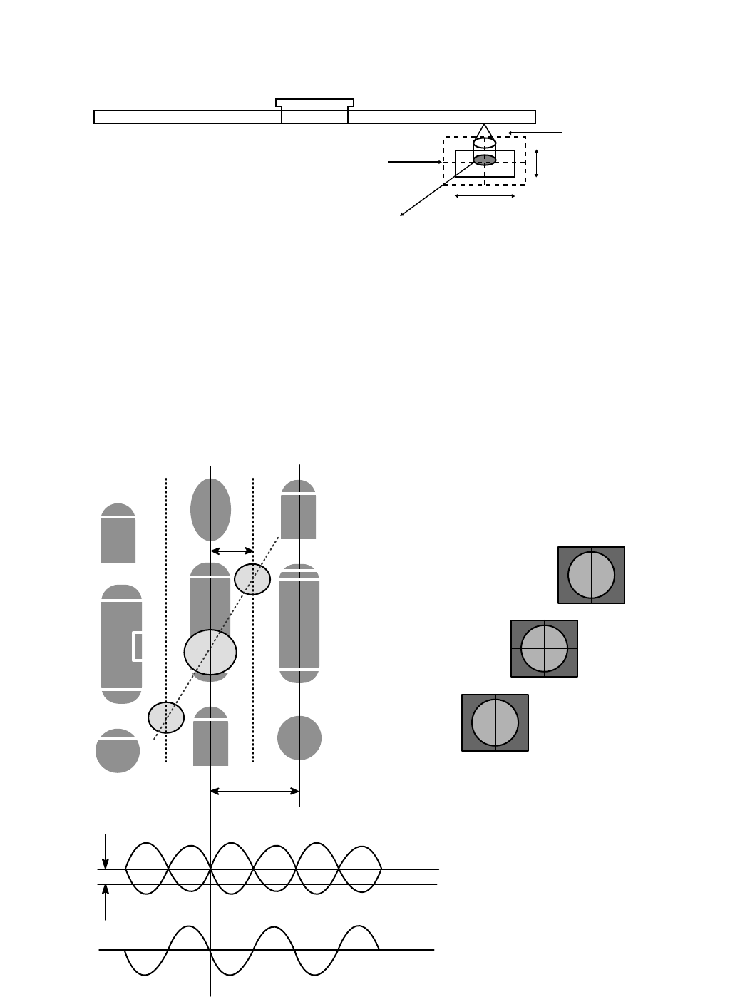
LOCATION OF CUSTOMER CONTROLS
10
1. Disc tray
This is the tray for the disc. Place the disc on the
ejected disc tray, then lightly push the tray (or
push the eject button) and the CD will be loaded.
NOTE: Don’t pull out or push in the disc tray
forcibly. This might cause damage to the loading
section of the drive.
2. Stop/Eject button
This button is pressed to open the CD tray.
This button works only when power is supplied to
the drive.
3. Emergency Eject Hole
Insert a paper clip here to eject the Disc tray
manually or when there is no power.
4. Drive activity indicator
Two colored LED is used to indicate the operation
of the Drive.
Drive Activity Indicators
Stop/Eject Button
Disc Tray
Emergency Eject Hole
Front Panel
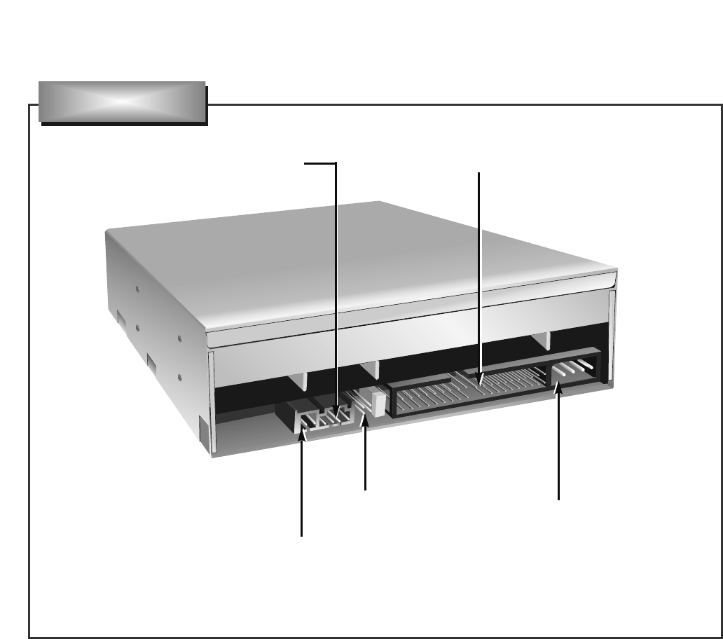
11
1. Power Connector
Connects to the power supply (5-and 12-V DC) of
the host computer.
NOTE : Be careful to connect with the proper
polarity. Connecting the wrong way may damage
the system (and is not guaranteed). Usually this
connector can only be attached one-way.
2. IDE Interface Connector
Connect to the IDE (Integrated Device
Electronics) Interface using a 40-pin flat IDE
cable.
NOTE : Do not connect or disconnect the cable
when the power is on, as this could cause a short
circuit and damage the system. Always turn the
power OFF when connecting or disconnecting the
cable.
3. Jumper Connector
This jumper determines whether the drive is
configured as a master or slave. Changing the
master-slave configuration takes effect after
power-on reset.
4. Analog Audio Output Connector
Provides output to a sound card (analog signal).
Generally you need this to play a regular audio
CD.
5. Digital Audio Output Connector
This connector is not supported.
Digital Audio Output
Connector
Jumper Connector
Analog Audio Output Connector IDE Interface Connector
Power Connector
Rear Panel
NOTE: The actual drive may be different from this design.
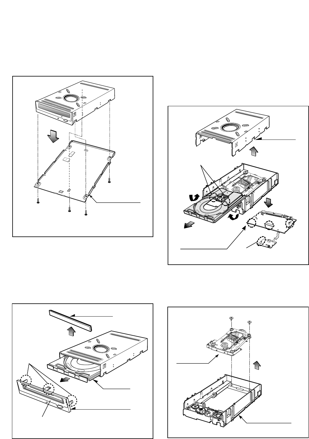
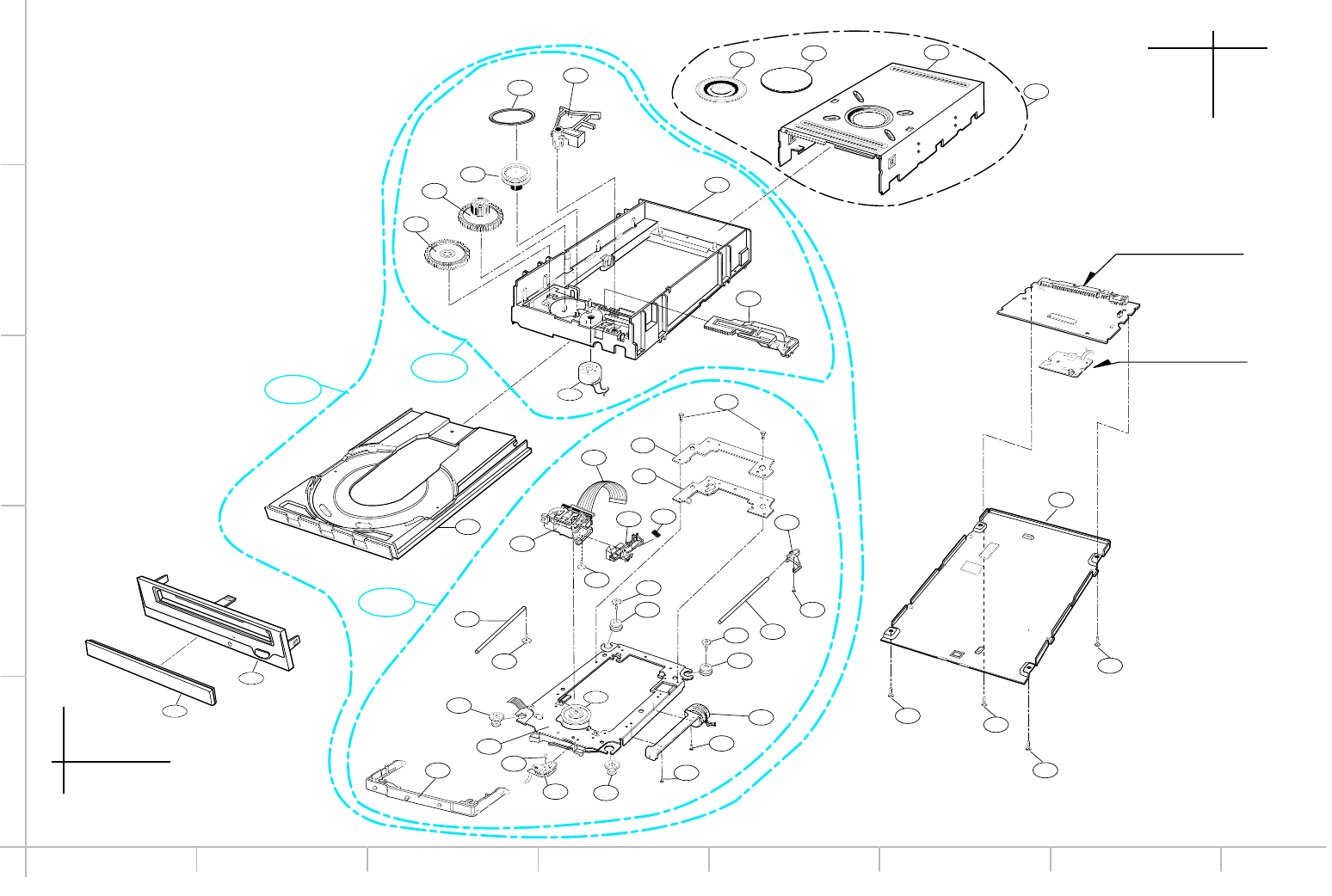
1. CABINET and CIRCUIT BOARD
DISASSEMBLY
1-1. Bottom Chassis
A. Release 4 screws (A) and remove the Bottom Chassis
in the direction of arrow (1). (See Fig.1-1)
1-2. Front Bezel Assy
A. Insert and press a rod in the Emergency Eject
Hole and then the CD Tray will open in the direction
of arrow (2).
B. Remove the Tray Door in the direction of arrow
(3) by pushing the stoppers forward.
C. Release 3 stoppers and remove the Front Bezel Assy.
1-3. Cabinet and Main Circuit Board
A. Remove the Cabinet in the direction of arrow (4).
(See Fig. 1-3)
B. When the CD tray has been opened completely, lift
2 points (a) and remove the CD tray while drawing
out simultaneously.
C. Remove the Soldering of the LD- and LD+ (b) for
the Loading Motor, and then remove the Main
Circuit Board.
D. At this time, be careful not to damage the 4
connectors of the Main Circuit Board.
2. MECHANISM ASSY DISASSEMBLY
2-1. Pick-up Unit
A. Release screws (B).
B. Separate the Pick-up Unit in the direction of arrow (6).
Main
Circuit Board
Cabinet
(4)
(5)
(a)
(b)
(A)
(A) (A)
(A)
(1)
Bottom Chassis
(2)
(3)
Tray Door
CD Tray
Front Bezel Assy
Emergency Eject Hole
Stoppers
Fig. 1-1
Fig. 1-2
DISASSEMBLY
12
Fig. 1-3
Mechanism Assy
Pick-up Unit
(6)
(B) (B)
Fig. 2-1
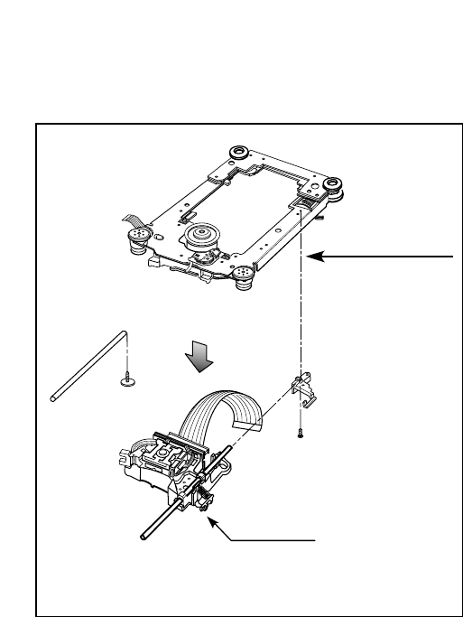
2-2. Pick-up
A. Release 1 screw (C) and remove the Pick-up.
Pick-up Unit
Pick-up
(C)
Fig. 2-2
13
030
014
007
A02
A01 A03
021
028
028
452
032
452
020
021
050
430
005 035 004
006
A B C D E F GH
1
2
3
4
5
452
024
481
034
027
026
033
025
430
445
020
453
031
036
453
010
011
009
008 012
016
015
013
PBM00 (MAIN C.B.A)
PBF00 (FRONT C.B.A)
482 482
482
001
482
003
002
(LightScribe only)
14 15
EXPLODED VIEW

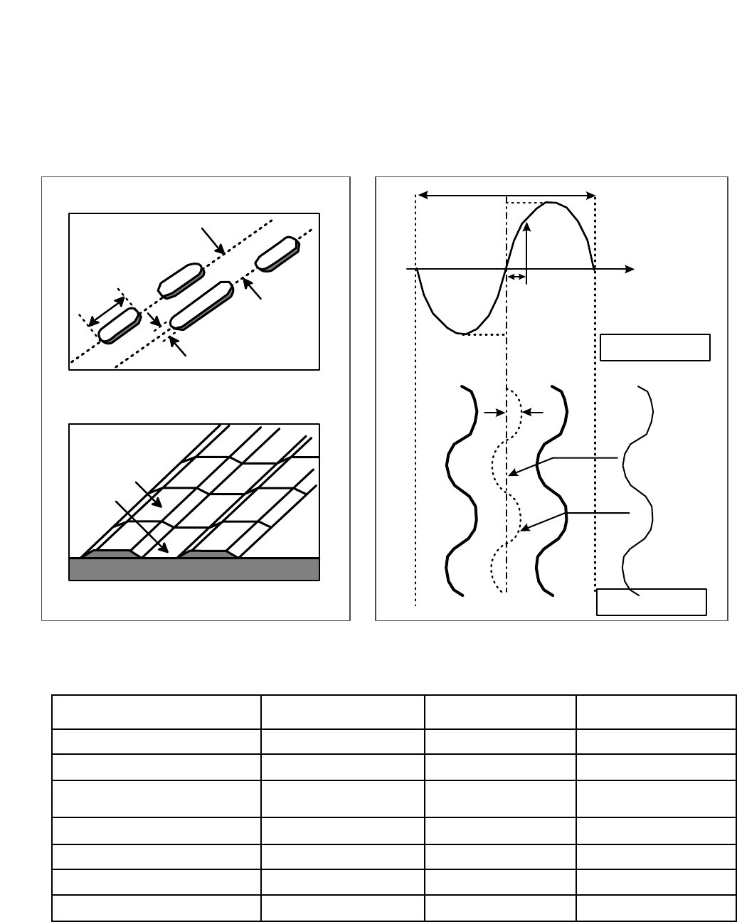
ATIP Absolute Time in Pre-groove. With an additional modulation of the “Wobble”, the “Groove” contains a time
code information.
Wobble The pre-groove in the Disc is not a perfect spiral but is wobbled.
With : – A typical amplitude of 30 nm
– A spatial peried of 54~64 µm
CW Continuous Wave. The laser light output is at a constant level.
DOW Direct Over-Write. The action in which new information is recored over previously recorded information in
CD-RW disc.
Overwrite
The action in which new information is recorded over previously recorded information.
(Pre-)Groove
The guidance track in which clocking and time code information is stored by means of an FM
modulated wobble.
Land Land is characterized in the following way:
When radial signals are concerned,land is defined as the area between the grooves.
When HF signal are concerned,land is defined as the area between the marks(pits) in tangential
direction.
Hybrid Disc A Multisession disc of which the first Session is mastered. On a hybrid disc, recorded and
mastered information may co-exist.
Mastered Information,stored as pits on the disc during the manufacturing process of the disc.
Information (when making the master)
OPC Optimum Power Control. Procedure is determined optimum recording power according to CD-
R/RW Media in recording start step.
ROPC Running OPC. The purpose is to continuously adjust the writing power to the optimum power
that is required.
When the optimum power may change because of changed conditions of disc and change in
operating temperature.
Jitter The 16 value of the time variation between leading and trailing edges of a specific (I3 … I11) pit
or land as measured by Time Interval Analysis.
Deviation The difference between a fixed value of Pit length and Land length.
TOC Table Of Contents : in the Lead-in Area the subcode Q-channel contains information about the
Tracks on the disc.
Packet A method of writing data on a CD in small increments.
Writing Two kinds of packets can be written : Fixed-length and Variable-length.
Write The shape of the HF write signal used to modulate the power of the laser.
Strategy The Write Strategy must be used for recordings necessary for disc measurements.
Information Wobble, ATIP, Disc Identification, Write Power, Speed Range OPC Parameters, etc are
Area recorded in the Information area of CD-RW Disc
Finalization The action in which (partially) unrecorded or logically erased tracks are finished and the Lead-in
and/or Lead-out areas are recorded or overwritten with the appropriate TOC subcode.
Logical Erase
A method to remove information from a disc area by overwriting it with an EFM signal containing
mode 0 subcode
A logically erased area is equivalent to an unrecorded
Physical Erase
The action in which previously recorded information is erased by overwriting with a CW laser
output.
After a Physical Erase action, the erased area on the CD-RW disc is in the unrecorded state
again.
Session
An area on the disc consisting of a Lead-in area, a Program area, a lead-out area.
Multi session
A session that contains or can contain more than one session composed Lead-in and Lead-out
GLOSSARY
19
20
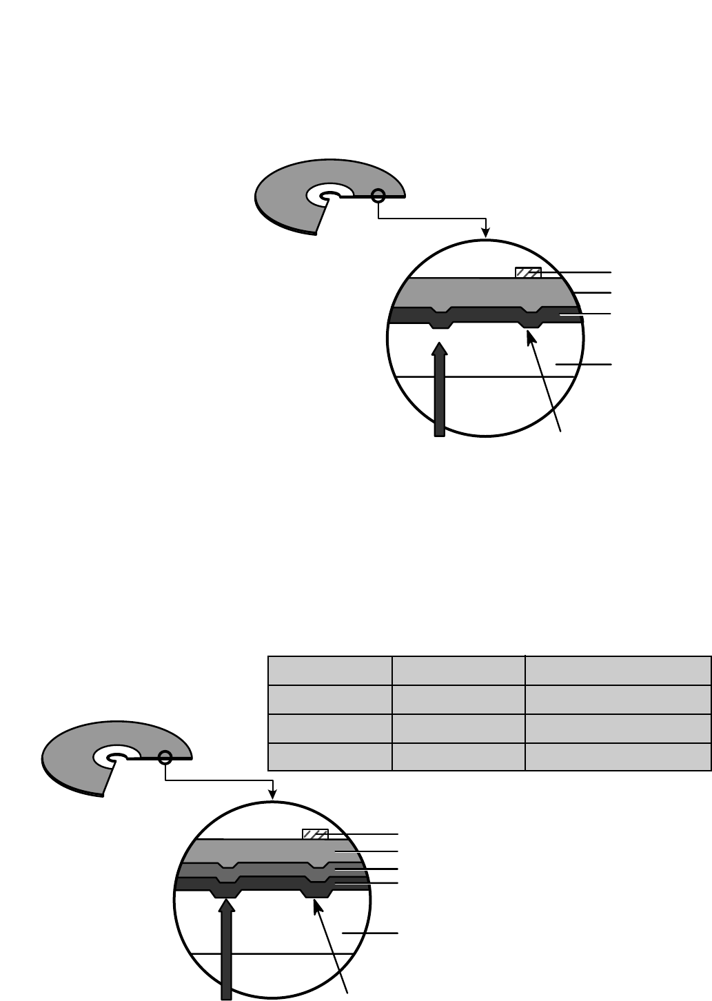
The differences of CD-R/CD-RW discs and General CD-ROM
1. Recording Layer
Recordable CD has a wobbled pre-groove on the surface of disc for laser beam to follow track.
2. Disc Specification
Read-only Disc
CD-R and CD-RW Disc
3~11T
1.6um
0.4~0.5 um
(Pit)Groove
Land
Track pitch(p)
Radial Direction
Iw
A
O
a
a
Groove
Land
Radial Error Signal
The Groove wobble
Average center
Actual center
CD-ROM (READ-ONLY DISC) a=30nm
ITEM CD-ROM CD-R CD-RW
Standard Yellow Book Orange Book II Orange Book III
Record Not available Write once Re-Writeable
Tracking Signal I11/Itop > 0.6 > 0.6 0.55 > M11> 0.70
(HF Modulation)
Read Laser Power(mW) < 0.5 mW < 0.7 mW < 1.0 mW
Jitter < 35 nsec < 35 nsec < 35 nsec
Reflectivity (Rtop) 70 % 65 % 15 % ~ 25 %
Remark) Write Laser Power(mW) 14-65 mW 6-45 mW
21
3. Disc Materials
1) CD-ROM disc
Laser Beam Groove
Substrate
(Polycarbonate)
Organic Dye Layer
Reflective Layer
Protective Layer
Label Printing
2) CD-R disc
Pigment Reflective Layer Color
Phtalocyanine Gold/Silver Yellow/White
Cyanine Gold/Silver Dark Green/Bright Green
Azo Gold/Silver Dark Blue
•It is composed of Silver _ colored aluminum plate and Reflective layer.
•Groove (Pit) of aluminum plate make a track.
•Laser wavelength : 780 nm, Laser Power (Read): 0.5mW
•Signal is detected by the
difference of reflective beam
intensity between “pit” and
“Land” on the disc.
•It is so-called WORM (Write Once Read Many) CD.
•It is composed of polycarbonate layer, Organic dye layer, Reflective layer, and Protective
layer.Gold/Silver Reflective layer is used to enhance the reflectivity
•According to the kinds of Organic dye layer, it is divided by Green CD, Gold CD, Blue CD.
•Laser Wavelength : 780 nm, Laser Power (read) : 0.7 mW
•Recording Power : 8x(14~20mW), 16x(25~35mW)
•When some part of dye layer is exposed to laser heat, it’s color changs black.Therefore, writing and
reading is enabled by the difference of reflectivity between changed part and unchanged part.
•Polycarbonate layer has Pre_Groove which make a Track.
Laser Beam
Pit
Substrate
(Polycarbonate)
Reflective Layer
Protective Layer
Label Printing
22
3) CD-RW Disc
4.
Reading process of Optical Disc
Laser Beam Groove
Substrate
(Polycarbonate)
Recording Layer
Dielectric Layer(TL)
Dielectric Layer(UL)
Protective Layer
Label Printing
•It is composed of polycarbonate layer, alloy(silver, arsenic) layer, aluminum reflectivity layer, protective layer.
•An crystalized alloy layer is transformed into noncrystalized by the laser heat. Therefore, writing and reading
is enabled by the difference of reflectivity.
•It is possible to overwrite about 1000 times.
•Laser Wavelength : 780 nm, Laser Power (Read) : 1.0mW
•Recording Power : Erase (4~18mW), Write (6~45mW)
•When disc rewriting, new data is overwritten previously recorded data.
•Polycarbonate layer has a Pre-Groove which make a track.
Lens HD
Beam
Spot
Focusing
Lens
Laser Spot
at Constant
Read Intensity
Reflected
Light
Signal
Laser Spot
Position
(Time)
Previously Recorded Marks
Groove Land Mirror
I3Itop
I11 IGILI0
Numerical aperture: NA=nsin
θ
,
n: Refractive index
Focus depth : H=
λ
/NA
laser spot diameter : D=
λ
/NA
2
θ
23
5. Writing Process of CD-R Disc
a b c d e f g
a
b
c
d
e
f
g
Incident
Laser
Power (Read) (Read)
(Write)
Laser Spot
Position
(Time)
a b c d e f g Laser Spot
Position
(Time)
Laser
Spot
Recorded
Mark
Reflected
Light
Signal
Reflected
Light
Signal
Below "ORP"– Mark Too Short
At Optimum Record Power ("ORP")
Above "ORP" – Mark Too Long
Time
6. Writing process of CD-RW Disc
Write Power
Erase Power
Read Power
Groove
Crystal Amorphous
Amorphous
Recorded state
(lower reflectivity)
Melting/
quenching
Heating/
gradual cooling
Crystal phase
Erased state
(higher reflectivity)
24
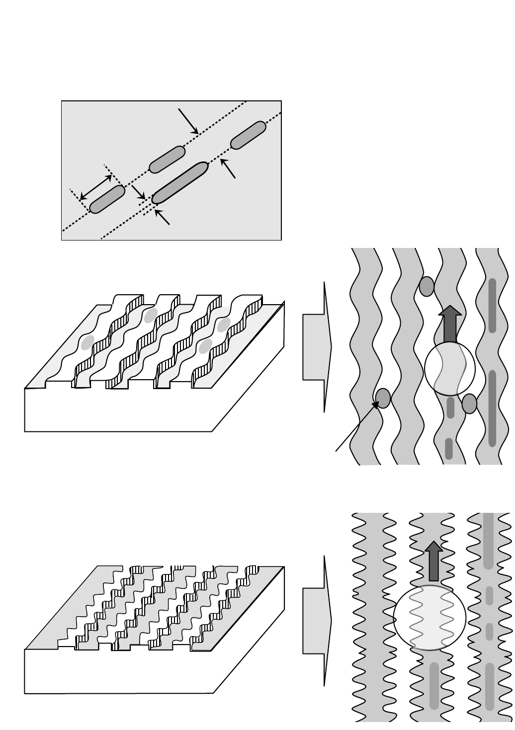
7. Organization of the PCA, PMA and Lead-in Area
1) Layout of CD-ROM disc
Center hole Clamping and Label Area Information Area
Lead-in Area
Lead-in Area
Diameter 15 mm
Diameter 46 mm
Diameter 120 mm
Program Area
Read Only Disc
Lead-out Area
Program Area Lead-out Area
Center hole Clamping and Label Area Information Area
PCA PMA
Test Area Count Area
Diameter 15 mm
Diameter 45 mm
Diameter 120 mm
Unrecorded Disc
Tsl-00:35:65 Tsl-00:15:05 Tsl-00:13:25 Tsl 99:59:74
00:00:00
in out
Test Area : for performing OPC procedures.
Count Area : to find the usable area immediately in T.A
Tsl : start time of the Lead-in Area, as encoded in ATIP
PMA : Program Memory Area
Disc Center
Disc Center
2) Layout of CD-R/RW disc

25
8. Function of PCA and PMA area
1) PCA (Power Calibration Area)
• PCA area is used to determine the correct Laser Power for a disc.
– Method 1 : PCA area is divided by a track.
– Method 2 : The previous Calibration value is referred.
– Method 3 : ROPC is used to determine Laser Power value automatically in data writing.
• CD-R Disc can write maximum 99 Tracks but CD-RW Disc can write unlimited tracks because it has a rewritable
function.
2) PMA (Program Memory Area)
• It has a track information (track No, track Start/End time) of every track before writing completed.
– PMA area has the last written point and the next writable point of a disc.
– In case of CD to CD copy, some writer may not write PMA area.
* When Disc is Finalized,
PMA information is transferred to the Lead_In area so that general Driver can read it.
* Because PCA and PMA area exist before Lead-In area, General CD Player or CD-ROM Drive can’t read
these areas.
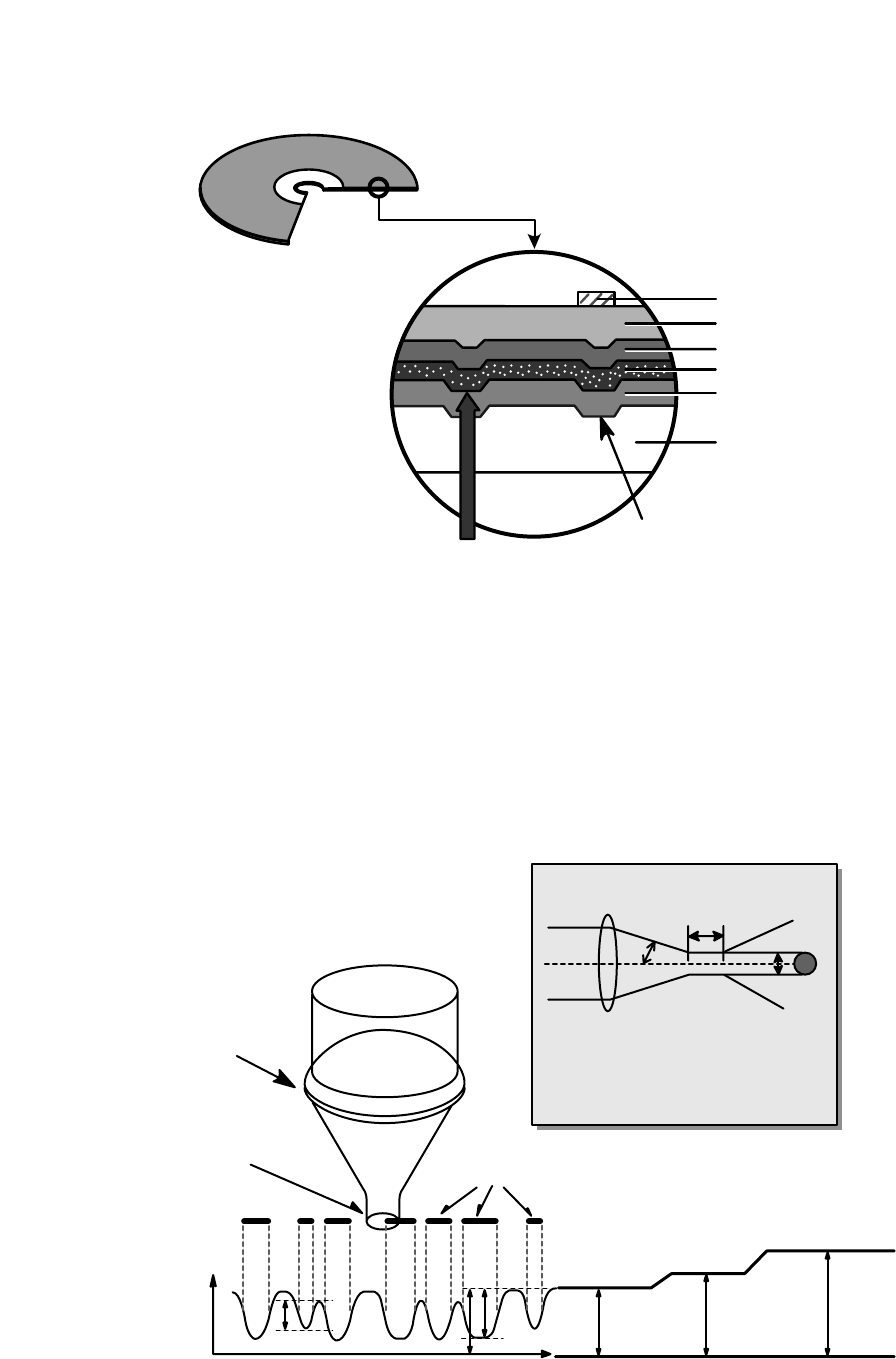
9. OPC and ROPC
1) OPC (Optimum Power Control)
• This is the first step of writing process, because CD writer has its own laser power value and media have different
writing characteristics,
– This is determined by the Writing characteristic, speed, temperature, and humidity.
– Laser wavelength is determined by the environmental temperature (775~795nm) and Optical Laser Power is
determined by the test and retry.
• Asymmetry and optimum writing Power
– EFM signal Asymmetry is determined by the writing power.
Therefore, Optical Power which has the same value to the preset power value can be estimated by measuring
HF signal Asymmetry on the PCA area.
• Measurement of Asymmetry
* Parameter setting (Beta) : Using AC coupled HF signal before equalization
Beta = (A1+A2)/(A1-A2)
Time P << Po Time P = Po
HF Signal
A1
0
A2
Time P >> Po
26
2) ROPC (Running Optimum Power Control)
• Variable primary factor of Optimum Power
– Change of Power sensitivity on the Disc. (limited to 0.05 *Po)
– Wavelength shift of the laser diode due to the operating temperature change.
– Change of the Spot aberration due to the Disc skew,
Substrate thickness, Defocus.
– Change of Disc or Optics conditions due to the long term OPC
==> It is necessary to adjust continuously to obtain the Optimum Power.
• Principle of Running OPC
– To meet the factors mentioned above,
a horizontal _ direction movement of a curve is uesd.
– Beta = f(B-level) = constant on the Recorded Disc
– Procedure of ROPC
a. Reference B-level is determined during OPC Procedure.
b. During Recording, B-level value is controlled to have a close
Reference B-level value.
c. Normalization of B-level is used to eliminate the effect of reflectivity fluctuation.
==> The reflected B-level value is normalized by the disc reflectivity itself.
CD-R/RW Media
Write Strategy
Determination
PCA Test Area
Program Area
PMA Area
Lead-In Area
Lead-out Area
OPC
PCA Count Area
ROPC
* Recording Capacity of CD-R/RW (74Minute Recording media)
•(2048 Byte/Sector) X (75 Sector/Second) X (60 Second/Minute) X 74 Minute
= 681,984,000 Bytes = 682 Mbytes
•But the actual recording capacity is about 650 Mbytes. (according to the ISO 9660 standard, approximately
30 Mbytes are used to make directory structure and volume names.)
Incident recording pulse
Reflected recording pulse
Sampled timing B
11T
Sample B-level (Write Power)
Level B
Sampled at timing B
Pwo decided by OPC
Recording Power
Level B with Pwo
normalized to recording power
Sample Disc Reflectivity
(Read power)
10. Writing Process of DISC
27
The differences of DVD-R/RW, DVD+R/RW discs and DVD-ROM
1. Recording Layer
LPP
(Land Pre-Pit)
DVD+R/RW Disc
DVD-R/RW Disc
0.74 um
3T
0.4 um
DVD-ROM (Read Only Disc)
28
2. Disc Specification
3. Disc Materials
1) DVD-ROM
DVD-ROM
Media Type
User data capacity
Single-Layer
Read Only
4.7GB
Dual-Layer
Read Only
8.54GB
DVD-R DVD-RW DVD+R DVD+RW
Dye Phase change Dye Phase change
4.7GB 4.7GB 4.7GB 4.7GB
Wavelength 650nm 650nm 650nm 650nm 650nm 650nm
Reflectivity 45~85% 18~30nm 45~85% 18~30% 45~85% 18~30nm
Track pitch 0.74 0.74 0.74 0.74 0.74 0.74
Minimum pit length 0.4 0.44 0.4 0.4 0.4 0.4
Modulation >0.6 >0.6 >0.6 >0.6 >0.6 >0.6
Channel bit- rate 26.16MHz 26.16MHz 26.16MHz 26.16MHz 26.16MHz 26.16MHz
Wobble Frequency - - 140KHz 140KHz 817.4KHz 817.4KHz
Addressing 26.16MHz 26.16MHz Wobble & LPP Wobble & LPP Wobble(ADIP) Wobble(ADIP)
Read Power (mW) 0.7 0.1 0.7 0.1
Write Power (mW) - -
JItter <8% <8% <8% <8% <9% <9%
++
Bonding layer
Polycarbonate
Semi-reflective
Polycarbonate
Reflective layer
Label
Polycarbonate
Label
Bonding layer
Reflective layer
Polycarbonate
<Single Layer >
<Dual Layer >
29
2) Recording format using organic dye material (DVD-R/DVD+R)
* The format that records data through the creation of recorded marks by changing the organic dye material
with a laser beam.
DVD-R
Adhesive layer
Protective layer
Reflective layer
Recording layer(dye)
Disc substrate
DVD+R
Adhesive layer
Protective layer
Reflective layer
Recording layer(dye)
Disc substrate
Adhesive layer
Protective layer
Reflective layer
Dye layer
Substrate
Laser beam
> Disc structure
> Disc structure
[Recording]
Recording is done by changing the organic dye layer and the substrate with a laser when a strong is
applied to a disc, the temperature of the ortanic dye material goes up, the dye is decomposed and the
substrate changes at the same time. At this time, a durable bit is created as is the case with a CD-ROM.
[Playback]
Signals are read with the differences of the reflection of a laser from pits.
30
3) Recording format using phase-change recording material (DVD-RW/DVD+RW)
* Data is recorded by changing the recording layer from the amorphous status to the crystalline status, and
played back by reading the difference of the reflection coefficient.
[ Amorphous : Non-crystalline ]
Substrate
Laser beam
Recording data
(Melting/Quick cooling)
Erasing data
(Heating/Gradual cooling)
Data erased state
(High reflection coefficient) Recorded state
(Low reflection coefficient)
Crystalline status Amorphous status
DVD-RW
Adhesive layer
Protective layer
Reflective layer
Dielectric layer
Recording layer
(Phase change material)
Dielectric layer
Disc substrate
DVD+RW
Adhesive layer
Protective layer
Reflective layer
Dielectric layer
Recording layer
(Phase change material)
Dielectric layer
Disc substrate
> Disc structure
> Recording principles
[Recording]
When a high-power laser is applied to the recording material, it melts and then becomes amorphous with
a low reflection coefficient when it quickly cools off. When a mid-power laser is applied to heat gradually
the recording material and then gradually cools it off, it becomes crystal with a high reflection coefficient.
[Playback]
A low-power laser is used for playback. The amount of reflected light depends on the status (amorphous
or crystalline) of the recording material. This is detected by an optical sensor.
31
4. Writing Pulse Wave Form of DVD+R
For different speed ranges, different write strategies can be used. This document specifies 2 options:
- a pulsed write strategy, where each single mark is created by a number of subsequent separated short
pulses.
- a blocked write strategy, where each single mark is created by one continuous pulse.
1) 1st Method : Using Pulsed Write Strategy
* 3T :
NRZI
T = 3
2Tw
Ttop
dTtop
dTle
Pb
top
top le
Pp
Channel bits
N = 3 : only the top pulse(T ),
first pulse lead-time dT , dT
NRZI
T > 4
2Tw Tw
Ttop Tmp Tmp Tlp
dTtop
dTle
Pb
top
top le
lp
mp
Pp
Channel bits
N > 4 : the top pulse (T ), multi-pulse (T ) and last pulse (T ),
first pulse lead-time dT , dT
Pp : Actual write power
Pb : Bias Power
* > 4T :
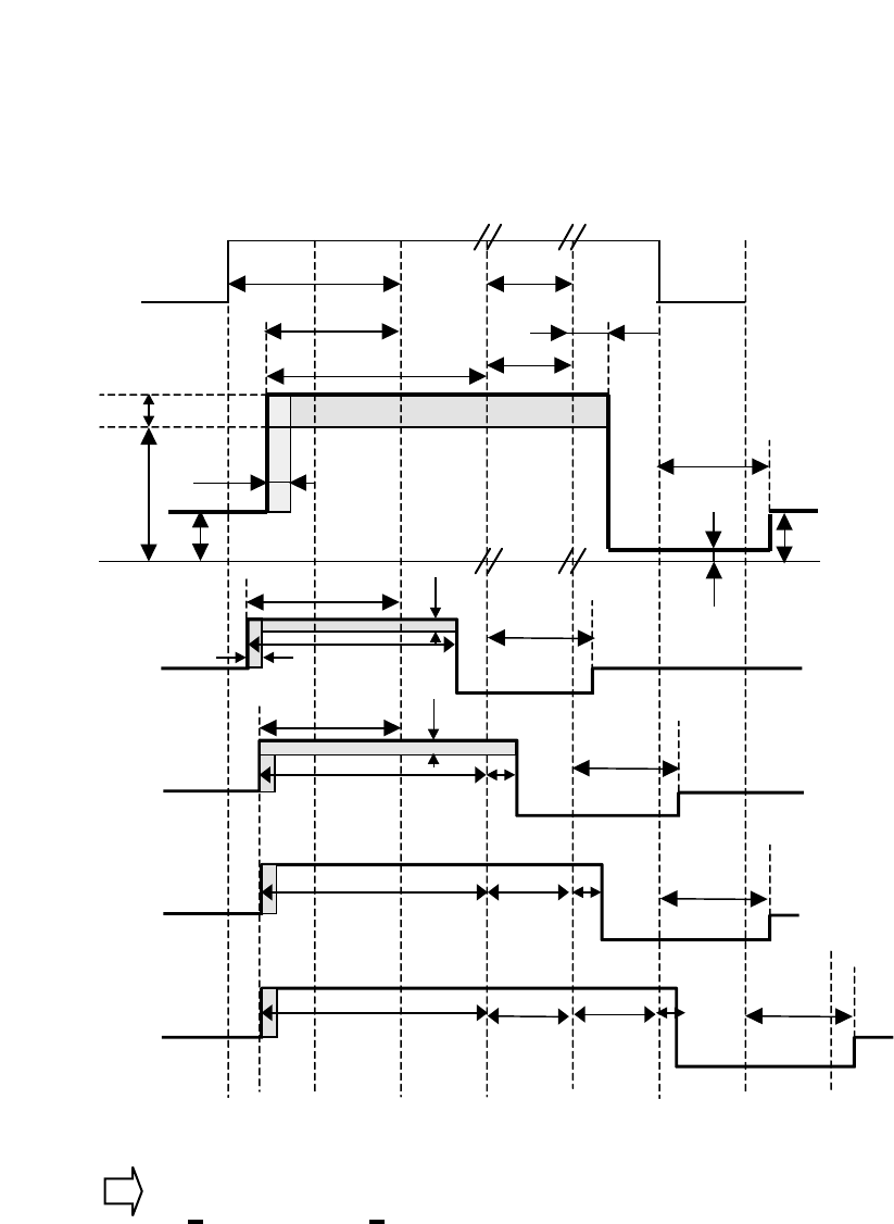
32
2) 2st Method : Using Blocked Write Strategy
NRZI
Channel bits 2Tw Tw
dT
top
Ttop
dTle
Pp
Pb
T
mp
lp
T
dPp
0mW PcPb
1.25Tw
3T mark
4T mark
5T mark
Etc.
dTtop,3 dP
p3
Ttop,3
dTle
1.25Tw
PcPb
1.25Tw
1.25Tw
1.25T
w
dTtop,4 dP
p4
Ttop,4 Tlp
Ttop,4
Ttop,4
Tmp
Tmp
Tlp
TlpTmp
N = 3 : T (cm = 3) can be optimized individually.
N > 4 : T (cm 4) + x (N-3) T + T , T = T
P shall be < 0.1mW
top
mp
lp
ww
top
c
Pp : Actual write power
Pb : Bias Power
dPp : Additional power ( Only be applied for the 3T and 4T marks)
Pc : Cooling power (Especially at higher recording speeds, optimum cooling down of the
recording layer after writing a mark may be needed.)
>
33
5. Writing Pulse Wave Form of DVD+RW
NRZI
Channel bits 2Tw Tw
Ttop
dTtop
Pp
Pe
Tmp mp
TdTera
Pp : Actual write power
Pe : Erase Power
Pb : Bias Power
Pb 0mW
T
mp
6. Organization of the Inner Drive Area, Outer Drive Area, Lead-in Zone and
Lead-out Zone
1) Layout of DVD-ROM disc
34
Center
hole
1st transition area
2nd transition area
Clamping
Zone 3rd transtion
area Information Zone
Lead-in Zone
Lead-in
Zone Lead -out
Zone
Diameter 15 mm
Diameter 16 mm
Diameter 22 mm
Diameter 33 mm
Diameter 44 mm
Diameter 120 mm
Data Zone
Read Only Disc
Lead-out Zone
Data Zone Outer Drive
Area
Inner Drive
Area
Inner Disc
Test Zone Outer Disc
Test Zone
Unrecorded Disc
PSN: 23080H 27080H 27480H 28480H 2A480H 30000H 260540H 261940H 262940H 263940H 267940H
in OUT
Disc Center
Rim area
Center
hole
1st transition area
2nd transition area
Clamping
Zone 3rd transtion
area Information Zone
Diameter 15 mm
Diameter 16 mm
Diameter 22 mm
Diameter 33 mm
Diameter 44 mm
Diameter 120 mm
Disc Center
Rim area
Inner Disc
Count Zone Outer Disc
Count Zone
2) Layout of DVD+R disc
> Inner Disc Test Zone : for performing OPC procedures.
> Inner Disc Count Zone : for counting the number of OPC algorithm performed in IDT Zone.
> Outer Disc Test Zone : for performing OPC procedures.
> Outer Disc Count Zone : for counting the mumger of OPC algorithm performed in IDT Zone.
3) Layout of DVD+RW disc
35
> Inner Disc Test Zone : for performing OPC procedures.
> Inner Disc Count Zone : for counting the number of OPC algorithm performed in IDT Zone.
> Outer Disc Test Zone : for performing OPC procedures.
> Outer Disc Count Zone : for counting the number of OPC algorithm performed in IDT Zone.
Lead-in Zone Lead -out Zone
Data Zone
Inner Disc
Test Zone Outer Disc
Test Zone
Unrecorded Disc
PSN: 2A480H 2A7C80H 2DC80H 30000H 260540H 262940H 265940H 266140H
in OUT
Center
hole
1st transition area
2nd transition area
Clamping
Zone 3rd transtion
area Information Zone
Diameter 15 mm
Diameter 16 mm
Diameter 22 mm
Diameter 33 mm
Diameter 44 mm
Diameter 120 mm
Disc Center
Rim area
Inner Disc
Count Zone Outer Disc
Count Zone
36
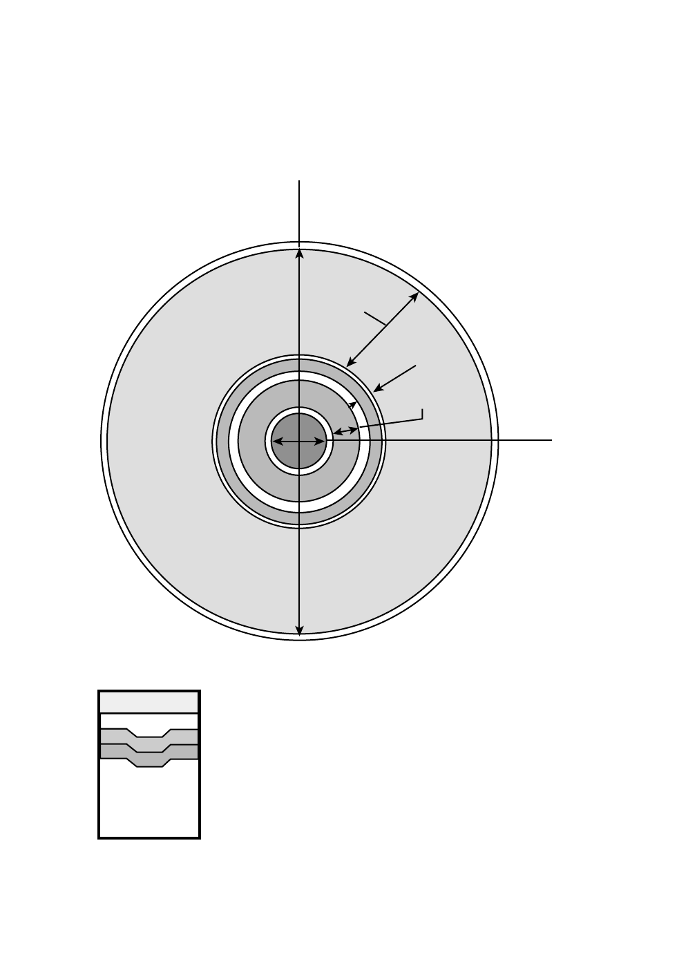
LightScribe Media
1. LightScribe Media
Center Hole
Screen Printed Imaging Layer
Clear Protective Coating
Reflective/Thermal Layer
Dye Data Layer
Polycarbonate
Substrate
DiscOD
Label Zone
Control Feature Zone
Clamping/Logo Zone
37
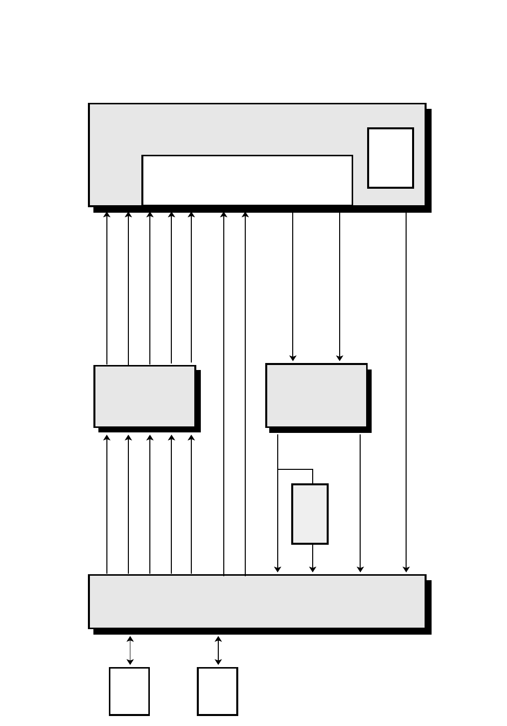
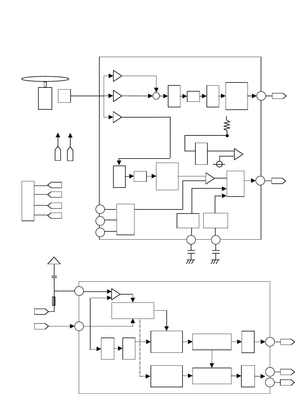
2. Hardware Block Diagram of LightScribe Label Printing
Host
PC
(Spindle)
uP
(DSP)
Power
Drive
Analog
Signal
Processor
MECHANISM
Optical
Pick-up
Optical
Encoder
(Sled)
(Track)
(Tilt)
(Focus)
RFOUT
Spindle Motor
Step Motor
Track Actuator
Tilt Actuator
Focus Actuator
Laser Power Reference
Write Strategy Control
Buffer
Memory
SERVO Signals
RF Cell Signals
Laser Power Monitor Signal
Optical FG
CIrcuit
38
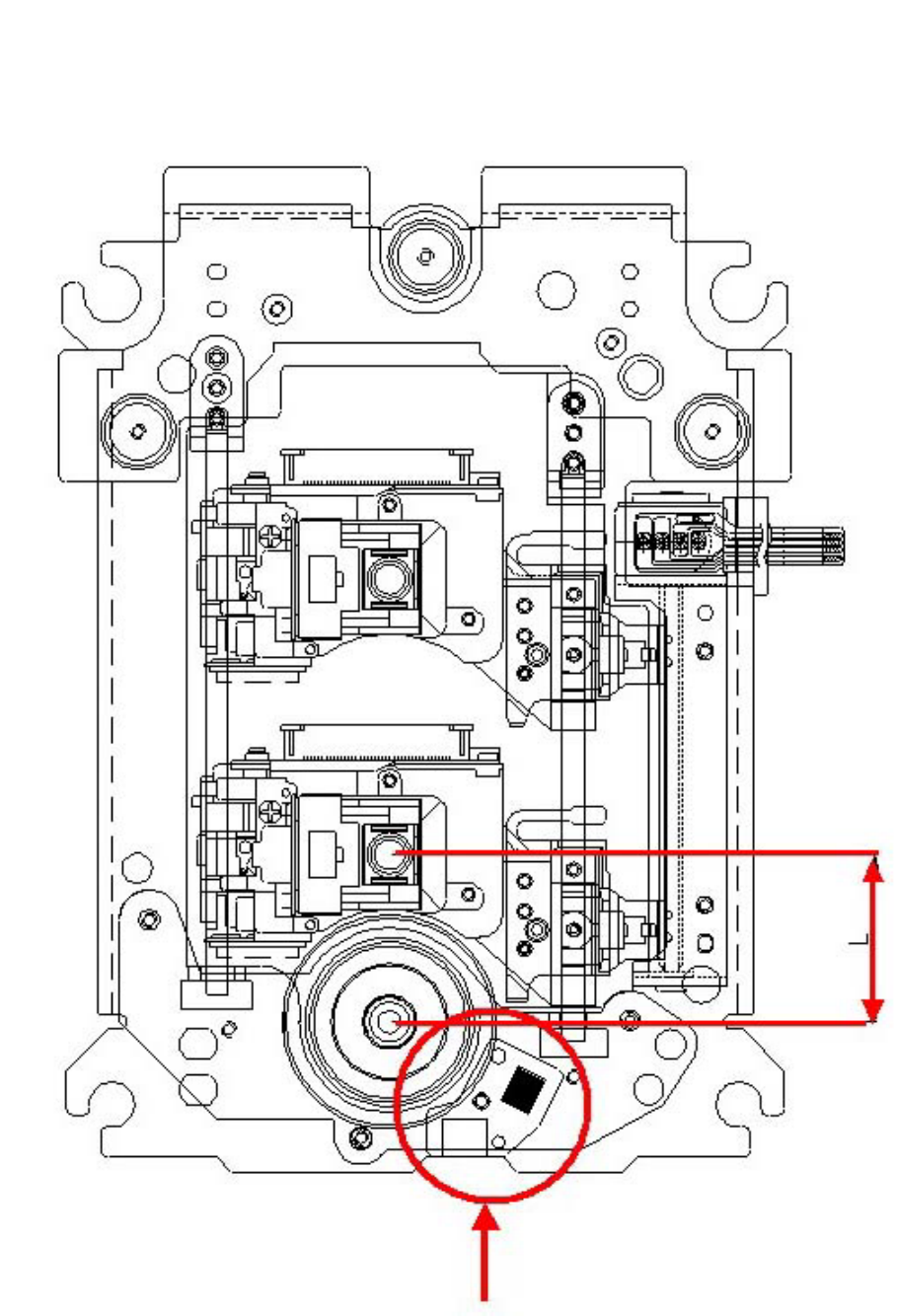
3. MD Assy For LightScribe
Optical Encoder Unit
OPU ID Movement Range : L=21um
39
4. Optical Encoder Assy
Codewheel
Direction of
radial play
CODEWHEEL
OR
CODESTRIP
FFC
3PIN SIGNAL
PROCESSING
CIRCUITRY
R
VLED
VCC
CH A
CH B
CH B
GND
GND
Vcc
OFG
Encoder PCB
PIN 6
VCC
PIN 5
CH A
PIN 4
GND
PIN 3
VLED
PIN 2
GND
PIN 1
CH B
PIN 6
VCC
PIN 5
CH A
PIN 4
GND
PIN 3
VLED
PIN 2
GND
PIN 1
CH B
Optical Encoder IC
Schematic of Enc PCB
40
DVD & CD DATA PROCESSING
1. Data Processing Flow
Command
Data
Status
RF EQ & AGC SERVO
DSP Encoder & Decoder & CSS
RF data slice EFM demodulator
CiRC error correction
Audio DAC
Buffer/Memory controller
CSS controller
Atapi interface control
Data PLL
Servo ADC
Focus/tracking
control output
Sled control output
CAV Spindle control
P-up
Unit
(HOP-7632TS)
IC101
RF AMP
(R2S35002) CD
DVD
IC301
(R8J32007)
TE/CSO GEN
FE GEN
DRAM
U-COM
SRAM
IC302
Flash ROM

41
R8J32007 HOST DVD
PLAYER
(EMPEG2 B/D)
Scrambled MPEG Data
Change the "KEY"
KEY Management Control
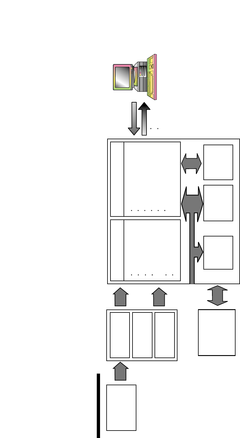
2. Copy Protection and Regional Code Management Block
Block Diagram
Brief Process
1. Regional Code for DVD Disc
– DVD-ROM drive transfers the regional code of the control data to host by the command of host, the DVD
player of host reads the regional code, and plays title in the case of allowed regional code only.
2. Management of DVD Disc for the scrambled of data
(1) DVD-ROM and DVD player of host generate the “KEY 1” respectively, transfer to opposite part, the
“KEY 2” is received, recognizes the data transfer or not with this value, and generates the bus key
encoded the data.
(2) Encoded “Disc Key” and “Title Key” host is transfer with the bus Key.
(3) DVD player of host reads the key value, and uses the value to restore the scrambled data.
* Refer to the next page for the details.
42
3. About Prevention the DVD-ROM from to be copy
A data is able to encode and record in the disc, if a copyright holder wants to prevent the disc from copying.
In case of a disc enhanced movie of 3 titles......
DISC KEY (2048 Bytes) is used to encode the whole contents in the disc and TITLE
KEY (5 Bytes) is used to encode the title respectively.
So, the data is encoded and stored in a disc through the unknown algorithms
with a disc key and title key. (At this time, the disc key and title key are stored
in a disc.)
…As above, the disc is able to copy when the disc key and title key are
opened.
Then, ROM-DRIVE encodes the disc key and title key and transfers to MPEG-
2 board.
If you want to play the disc prevented from the copy......
First of all, ROM-DRIVE and MPEG-2 board identify with each other through the procedure as described
below.
1. Drive and host gives and takes the ID of 2bit. This ID is AGID (Authentication Grant ID).
The various decoder boards are attached to the host, in these, AGID sets the MPEG-2 board and drive.
2. After the AGID is set, MPEG-2 board generates the challenge key (10 Byte) and transfers to drive. The
board and drive generate key 1 (5Byte) with the challenge key respectively. (Of course, the Algorithm
generating the key 1 is not known.)
3. Compare with the generated key 1, if it corresponds each other, the first step of authentication is
completed. This is a course to identify the MPEG-2 board with a drive.
4. The second step of authentication is a course to identify a drive with the MPEG-2 board.
The dirve generates a challenge key and transfers it to the MPEG-2 board. The dirve and MPEG-2 board
generate the key 2 (5Byte) with the challenge key, compare with each other, and if it corresponds and the
secondary step of authentication is completed.
5. As above, the identification is completed.
6. The dirve and MPEG-2 board generate the Bus key with the key 1 and key 2 and own it.
7. Dirve encodes the disc key and title key with this Bus key and transfers to the MPEG-2 board.
8. The MPEG-2 board reads the encoded disc key and title key with the Bus key only.
9. MPEG-2 board lets data read from the drive to decode with the read disc key and title key and makes into
the video signal by decoding.
ROM-DRIVE
AGID HOST
MPEG-2
BOARD
Challenge key
encoded disc key, title key
43
4. About the DVD-ROM Regional Code
DISC ROM - DRIVE MPEG-2 BOARD VGA CARD MONITOR
1
CAN
U.S.A
MIX
CUB
BHS
PRI. VIR
1
BMG
GRL
2
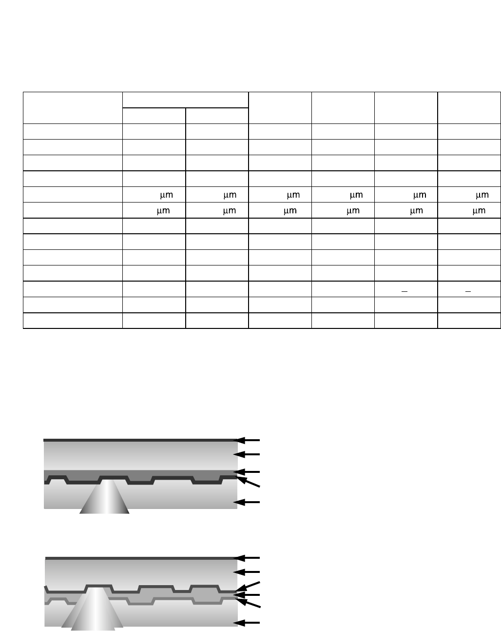
2ZAF
ISO
SWZ
FIN
POI
FST
LTU
BIR
UKR
TUR
FGY
JRN
TKM
AFG
PAK
CHN
MMR
MNG
RUS
KOR JPN
HKG
MAC TWN
PHL
6
3
21
5
5
4
1
MDI
MNP
GUM
PLW
PNG
NZL
AUS
4
The disc has
the regional
code of 8 bit.
Example)
The disc
manufactured
in the U.S.A,
has the
number one.
Transfer to
MPEG-2 board
reading the
regional code.
Receiving
data from the
MPEG-2
board and
output
through the
monitor
If the board is setting to the regional
code 1 for the U.S.A. ...
Check the received regional code to
number 1, all or not, transfer the
data to VGA card in accordance with
only a case among the three case.
Regional code
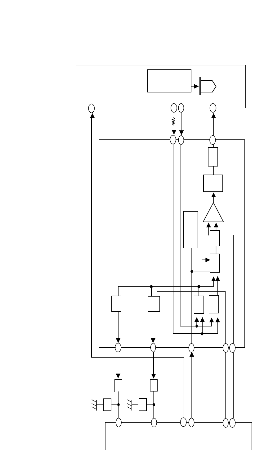
INTERNAL STRUCTURE OF THE PICK-UP
1. Block Diagram of the PICK-UP(HOP-7632TS)
44
45
16 15 14 13 12 11 10
26 27 28 29 30 31 32
917
8
7
6
5
4
3
2
1
Tilt-
C3
R1
R4
CD-LD
DVD-LD
R2
FB2
FB1
CD-VR
DVD-VR
GND EF4
EF1
VA
VB
VEF2
VREP
VRFN
VD
VCC
VS
VC2
VEF3
SW
C15
C14
C6 C5
C9
C10
Rth
R7
R8
R14
Rd
C12
C13
FB3
C2
C1
IC2(LDD)
IC2(FM)
IC3(OEIC)
VSO
18 OUT2
19 OUT2
20 VSO
21 VSO
22 GND
23 OUT1
24 OUT1
25 VSO
NC
NC
BUSY
SEN
SDIO
SCLK
MON1
VSL
CLK
CLKB
GND
GND
NRZB
NRZ
RWB
VSA
RSET
EN
AGND
ISLOP
IAPC
Rfreq
SLG
44 Tilt+
43 TR-
42 TR+
41 AF-
40 AF+
39 GND(FM)
38 FM
37 VREF
36 SEL
35 VCC(FM)
34 ENA
33 IAPC
32 SLG
31 VSA5
30 VSL25
29 CLK
28 CLKB
27 GND(LDD)
26 NRZB
25 NRZ
24 GND(LDD)
23 MONITOR
22 RWB
21 SDIO
20 SCLK
19 BUSY
18 SEN
17 VSO
16 Vcc(FM)
15 GND(OEIC,TEMP)
14 RF-
13 RF+
12 E2+F2
11 C
10 A
9E1+F1
8E4+F4
7D
6B
5E3+F3
4GAINSW
3Vc(OEIC)
2Vcc(OEIC)
1GND(OEIC,TEMP)
54
2
1
6
7
7F4 F1
F3 F2
E4 E1
DA
BC
E3 E2
8
9
10
11
12
13
14
6
5
4
3
2
1
3
Behind View DVD-LD : 1st Vendor : Rd = 82k
DVD-LD : 2nd Vendor : Rd = 5.6k
8

45
2. Pick up Pin Assignment
No. Signal Name I/O Signal Description
1 GND(OEIC,TEMP) Ground for OEIC
2 Vcc(OEIC) I Power supply for OEIC
3 Vc(OEIC) I Reference voltage input for OEIC
4 GAINSW I OEIC output gain control (High:Low gain, Middle:Middle gain, Low:High gain)
5 E3+F3 O Single OEIC output EF3
6 B O Single OEIC output B
7 D O Single OEIC output D
8 E4+F4 O Single OEIC output EF4
9 E1+F1 O Single OEIC output EF1
10 A O Single OEIC output A
11 C O Single OEIC output C
12 E2+F2 O Single OEIC output EF2
13 RF+ O Single OEIC RF positive differential output
14 RF- O Single OEIC RF negative differential output
15 GND(OEIC.TEMP) O Ground for OEIC and TEMP
16 TEMP O Output voltage for controlling temperature
17 VSO I Supply voltage for the output drivers only
18 SEN I Serial control enable (H=enable, L=disable)
19 BUSY O Goes high when serial transfer to timing menory is active
20 SCLK I Serial control clock
21 SDIO I/O Serial data for parameters and control ; in/out
22 RWB I Write enable for NRZ laser data (L=write, H=read)
23 MONITOR O Monitor output
24 GND(LDD) Ground connection for LD Driver-IC
25 NRZ I NRZ laser data (H=mark, L=space) (LVDS+)
26 NRZB I NRZ laser data (H=mark, L=space) (LVDS-)
27 GND(LDD) Ground connection for LD Driver-IC
28 CLKB I CLOCK for NRZ code input (LVDS-)
29 CLK I CLOCK for NRZ code input(LVDS+)
30 VSL25 I Supply voltage for 2.5V logic
31 VSA5 I Supply voltage for PLL only
32 SLG I Land/groove input serects the power register set (H=land, L=groove)
33 IAPC I A low inpedance current input ; 100xIAPC frow to the output
34 ENA I Fast chip enable input
35 VCC(FM) I Power supply for FM
36 SEL I Low: selects DVDFMOUT
High: selects CDFMOUT
37 VREF I APC amplifier reference voltage input
38 FM O APC amplifier output
39 GND(FM) Ground connection for FM
40 AF+ I Focusing Actuator drive signal+
41 AF- I Focusing Actuator drive signal-
42 TR+ I Tracking Actuator drive signal+
43 TR- I Tracking Actuator drive signal-
44 Tilt+ I Tilting Actuator drive signal+
45 Tilt- I Tilting Actuator drive signal-
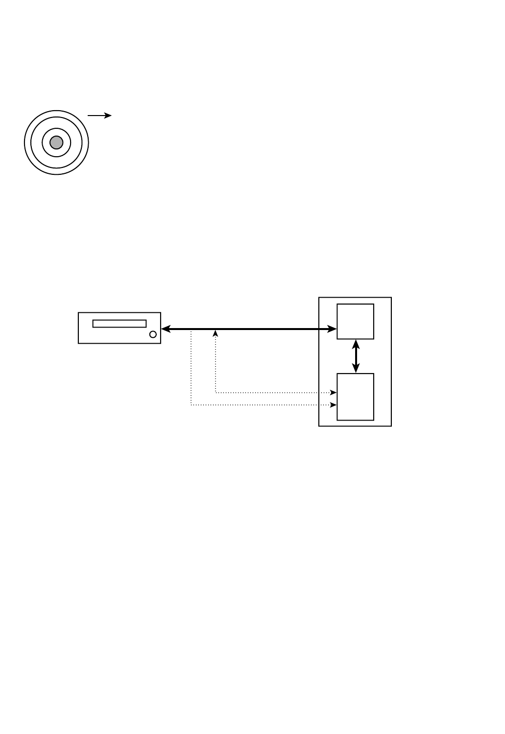
3. Signal detection of the P/U
1) Focus Error Signal ==> (A+C)-(B+D)
This signal is generated in RF IC (IC101 : R2S35002) and controls the pick-up’s up and down to focus on
Disc.
2) Tracking Error Signal (DPP Method) ==> {(A+D)-(B+C)}- kx {(EF1+EF4)-(EF2+EF3)}
This signal is generated in RF IC (IC101 : R2S35002) and controls the pick-up’s left and right shift to find
to track on Disc.
3) RF Signal ==> (A+B+C+D)
This signal is converted to DATA signal in DSP IC (IC301 : R8J32007).
46
Pick-Up module
Photo Diode Tracking
Focusing
Infrared Iaser
k[(F+H) - (E+G)]
(A+D) - (B+C)
(A+D) - (B+C) - k[(F+H) - (E+G)]
Offset
TE
Tp
Sub2
Main
Tp/2 Sub1
Track Center
F,E
D,C
A,B
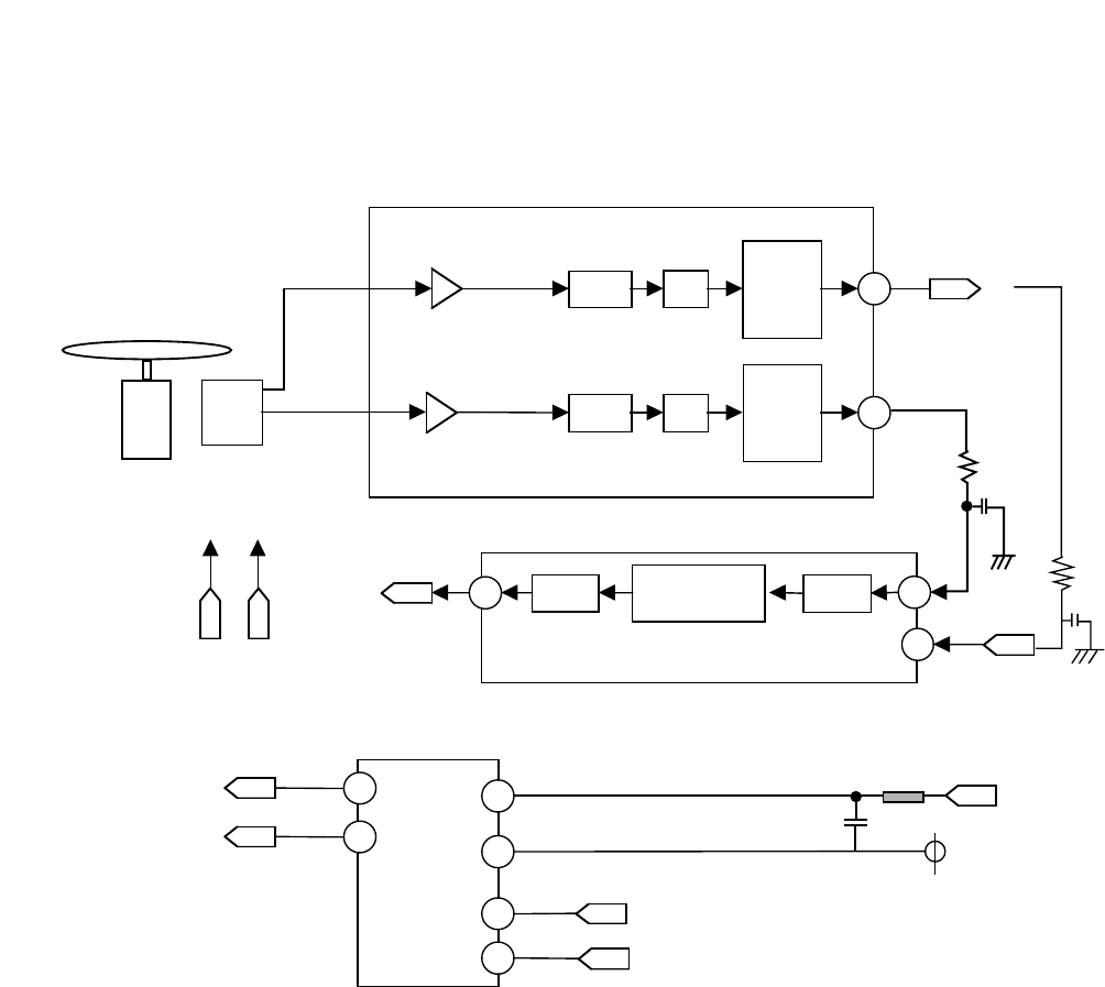
H,G
47
WGATE
RFPDSH
Optical
Pick-up
LD
Driver
Write
Strategy
FsDAC
WDAC
IAPC
R160
LPF
&
Gain
WFPDSH
FMON
RWAPC
buffe
r
2.5VREF
Buffer
S/H
B/H
+
-
13 S/H MU
X
AM
P
APCDAC
(REDA/WRDA)
SCLK, SDATA, WDEN
12
99
810
28
29
126
127
CN101 IC101 (R2S35002))
IC301 (R8J32007)
BCNT
5
6TCPH
32 134
175
R106
R105
C106
25,26,28
120,121,123
108
C105
DESCRIPTION OF CIRCUIT
1. ALPC (Automatic Laser Power Control) Circuit
1-1. Block Diagram

48
1-2. ALPC (Automatic Laser Power Control) Circuit
ALPC function DVD/CD anlaog front-end IC(IC101 R2S35002) is for constant power control purpose. Based on the
accurate power sensor(FMON) in P/U, ALPC feedback loop maintains constant power level against laser diode’s
temperature variation.
The ALPC loop amplifies(10x) the FMON signal to enhance the accuracy of read power level control. Swithching of
amplification is made by combination of a logical WGATE signal and a logical RWAPC signal.
There are two set of APCDAC, which are used at different term to monitor different power level. Generally, the one is used
at reading and the other one is used at writing. The logical WGATE signal which is switched between reading and writing
changes the two APCDAC.
The ALPC loop supplies same currency (IAPC) to Laser Diode Driver(LDD) during reading and writing.
There is another ALPC which controls Full-Scale-DAC (FsDAC). FsDAC determines scale of WDAC of Laser Diode Driver.
MPU monitors write-power level of FMON signal and changes FsDAC directly to maintain constant write-power level. There
are two write power signal. The one is based on S/H signal and the other one is based on B/H(Bottom-Hold) signal. The
write power levels are monitored as digital levlels which are converted by built-in Anlog-Digital Converter in DSP. The MPU
monitors each write power level and calculates proper setting of FsDAC, and changes value through serial interface
between LDD and DSP.
49
2. Focus Circuit
2-1. Block Diagram
Disc
Motor unit Optical
Pick-up
HOP-7632TS
A,B,C,D
A,B,C,D
(EF1~EF4)
(A+C)-(B+D)
(A+C)-(B+D)+K[(EF1+EF3)-(EF2+EF4)]
HAVC
LS
to
V14 FE
FE
FE
R102
C405
R103
C406
GND
GND
ADC
Focusing
Compensator
DAC
FOD
FOD
R329
R2S30202FP
IC601
FACT+
FACT-
FACT+
FACT-
IC101
R2S35002
IC301
R8J32007
EN1
EN2
CTL1
CTL2
C335
REF 1.65V
FOIN
A+B+C+D
LPF G
HAVC
LS
to
0.8V
PE
PE
3
LPF G2
169
170
180
40
42
20
21
34
35
2-2. Focus Servo
The aim of Focus Servo is to maintain the distance between object lens of P/U and disc surface, so that the
detected RF signal(A, B, C, D, EF1, EF2, EF3, EF4) can be maximized.
Focus Error Signal(FE) generates from focus error detection block in RF IC(R2S35002) using Conventional
Astigmatism Detection method, Differential Astigmatism Detection method.
Focus Gain and path can be changed at the RF IC(R2S35002) according to the disc, and the resulting output
FE(R2S35002 2pin) is input to DSP IC(R2S35002 169pin).
The Focus Search operation is using FE, PE Signal, therefore check FE, PE signals when Focusing is failed.
The role of DSP IC(R8J32007) is Focus Digital Controller. The operation path is as follows;
FE Signal is input to DSP IC(R8J32007 169pin), and after A/D Conversion, Digital Equalizer Block and D/A
Conversion in R8J32006FP, the output signal FOD(R8J32007 180pin) is input to Drive IC(R2S30202FP 40pin).
The drive output signal FACT+/FACT- generated according FOIN(R2S30202FP 40pin), and drives focus
actuator in the P/U unit.
50
3. Tracking & Sled Circuit
3-1-1. Block Diagram (Tracking Following)
Disc
Motor unit Optical
Pick-up
HOP-7632TS
A,B,C,D
(EF1~EF4) TE
TE
R101
C101
GND
TE
ADC
Tracking
Compensator
DAC
TRD
TACT+
TACT-
IC101
R2S35002
IC301
R8J32007
MPPO
(A+D)-(B+C)
G
HAVC
LS
to
V14
1
173
181
L
P
F
L
P
F
SPPO
(A+D)-(B+C)-K[(EF1+EF4)-(EF2+EF3)]
Sled
Compensator
DAC
SL2
183
SL1
182
A+
A-
B+
B-
SLED MOTOR
Unit
(CN601)
TRD
R330
IC601
R2S30202FP
TACT+
TACT-
EN1
EN2
CTL1
CTL2
REF
C604 1.65V
TOIN
39
42
20
21
36
37
SL2
2
SL13
SL1IN
SL2IN
A-
B-
8
10
A+
B+
6
9
SL2N
SL1N
SL2P
SL1P
C336
1.65V
C338
C337
R372
1.65V
R374
R373
R332
R331
3-1-2. Block Diagram (Seek)
51
Disc
Motor unit Optical
Pick-up
HOP-7632TS
SUMF
RFIP
RFIN
(EF1~EF4)
A,B,C,D
TACT+
TACT-
IC101
R2S35002
MPPO
(A+D)-(B+C)
G
HAVC
LS
to
V14
1
L
P
F
L
P
F
SPPO
[(EF1+EF4)-(EF2+EF3)]
A+
A-
B+
B-
SLED MOTOR
Unit
A+B+C+D
G
HAVC
LS
to
V14
L
P
F
L
P
F
38
79
80
81
EQ
MIRR
DET
AGC TOP
HOLD
63 62
BOTTOM
HOLD
-
+
-
+
TE1
MIRRTOPH MIRRBOTH
C128
GND
MIRR
VREF1
VREF1
SL2
D
A
C
Tracking
Compensator
IC301
R8J32007
173
Sled
Compensator
A
D
C
149
M
U
X
Short
Seek
Algorithm
Loog
Seek
Algorithm
D
A
C
182
181
183
TRD
SL1
Track Counter
and Timer
R101
C101
GND
MIRR
TE1
TE
IP2MIRR
C127
GND

52
3-2-1. Tracking Servo
The aim of tracking servo is to make laser beam trace the data track on disc.
Tracking Error(TE) Signal is generated from tracking error detected block in R2S35002 using DPP(Differential
Push-Pull) Method and DPD (Differential Phase Detection) Method.
DPP Method uses not only main beam(A, B, C, D) but also side beam(EF1~EF4) for correcting DC offset
generated in Push-Pull Method.
The remaining procedure of TE signal processing in R8J32007 is similar to Focus Servo.
The role of DSP IC(R8J32007) is Tracking Digital Controller.
TE Signal is input to DSP IC(R8J32007 173pin), and after A/D Conversion, Digital Equalizer Block and D/A
Conversion in R8J32007, the output signal TRD(R8J32007 181pin) is input to Drive IC(39pin).
The drive output signal TACT+/TACT- generated according TOIN(R2S30202FP 39pin), and drives tracking
actuator in the P/U unit.
3-2-2. Sled Servo
The working distance of tracking actuator is too short to cover whole disc radius.
Sled Servo make P/U move by little and little so that the laser beam keep tracing the data track on disc
continuously when tracking actuator reaches the working limit.
TE Signal is input to DSP IC(R8J32007 173pin), and after A/D Conversion, Digital Tracking Equalizer Block,
Digital Sled Compensator Block and D/A Conversion in R8J32007, the output signal SL1, SL2(R8J32007 182,
183pin) is input to Drive IC (R2S30202FP SL1:3 pin, SL2:2pin) after Low-Pass filtering.
4. Spindle Circuit
4-1-1. Block Diagram(FGCAV Servo)
53
Disc
Motor unit
Optical
Pick-up
HOP-7632TS
XCO
Control Clock
Generator
IC301
R8J32007 107
M
U
X
P
W
M
SPD
211
Motor Kick
REG
CAV FD
+
CAV PD
SFG
VCK4M
VCK4M 106
R349
C349
R375
1.65V
SPD
IC601
R2S30202FP
U
V
CTL1
CTL2
DAVC 1.65
1
20
21
12
13
19
42
SPD
SFG
CTL2
CTL1
SPIN
FG
W14
XCI
213
R361
3.3V
X301
33.8688MHz
4-1-2. FG CAV Servo
1) CD 48x CAV : CD-ROM, CD-R
2) CD 40x CAV : CD-RW
3) DVD 8x CAV : DVD+RW
4) DVD 10x CAV : DVD+R
5) DVD 12x CAV : DVD-ROM DL
6) DVD 16x CAV : DVD-ROM
7) DVD 16x PCAV : DVD+R
When drive read PRESS CD, Closed Session CD-R/RW, the spindle motor is controlled using FG CAV Spindle
Servo. FG signal(R2S30202FP 19pin) input to SFG in DSP IC(R8J32007 213pin).
The spindle controller in DSP IC uses SFG as spindle rotation frequency feedback, therefore the FG CAV
Spindle Servo doesn't work well if FG generation is abnormal.
The spindle controller PWM output signal SPD(R8J32007 211pin) input to SPIN in Drive IC(R2S30202FP 1pin)
after Low-Pass Filtering.
The PWM output signal U, V, W signal(R2S30202FP 12, 13, 14pin) drives Spindle Motor without using a
sensor, and FG pulse output is generated as 18 pulses/rotation.
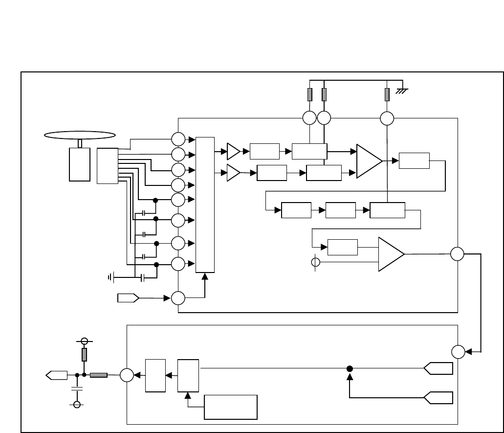
4-2-1. Block Diagram (Wobble CLV Servo)
54
Disc
Motor unitOptical
Pick-up
HOP-7632TS
IC101
R2S35002
HPF
S
/
H
-
+
C174
C173
C171
C172
WBLSH
C116
87
88
89
90
92
93
94
95
HPF AGC2
HPFBPF AGC3
HPF
HPF 37
31
WBLS
GND
H
18 19
AGC1
20
VREF
WAG1 WAG2 WAG3
SA
SB
SC
SD
MA
MB
MC
MD
+
-
C117 C118
ADO
BCO
IC301
R8J32007
M
U
X
P
W
M
SPD
PH
SP
211
Motor Kick
REG
154
R349
R375
C349
1.65V
1.65V
SPD
WOBSIG
4-2-2. Wobble CLV Servo
CD-R : 4x, 8x, 16x, 24x, 32x, 40x, 48x
/CD-RW : 4x, 10x, 16x, 24x, 32x
/DVD-R : 2x, 4x, 8x, 16x(PCAV)
/DVD-R DL : 2x, 4x
/DVD-RW : 1x, 2x, 4x, 6x
/DVD+R : 2.4x, 4x, 8x, 12x, 16x(PCAV)
/DVD+R DL : 2.4x, 4x, 6x
/DVD-RAM : 2x, 3x, 3-5x(PCAV)
/DVD+RW : 2.4x, 4x, 8x
When drive write DVD-RAM/R/RW/+R/+RW/CD-R/CD-RW, the spindle motor is controlled using Wobble CLV
Spindle Servo.
The WOBSIG signal(R2S35002 37pin) input to DSP IC(R8J32007 154pin). The DSP Controller in R8J32007
uses WOBSIG as linear velocity feed back, therefore the Wobble CLV Spindle Servo doesn’t work well when
WOBSIG signal is abnormal.
The spindle controller PWM output signal SPD (R8J32007 211pin) input to SPIN in Drive IC(R2S30202FP 1pin)
after Low-Pass Filtering.
The PWM output signal U,V, W signal(R2S30202FP 12, 13, 14pin) drives Spindle Motor without using a sensor.

MAJOR IC INTERNAL BLOCK DIAGRAM AND PIN DESCRIPTION
IC101 (R2S35002) : RF AMP Analog Signal Processor
Pin Assignment
55
75
PORT13
74
PORT12
PORT11
PORT10
73
AGHPF1
72
AGHPF2
71
VDD1(3.3V)
70
EQOP
69
EQON
68
GND1
67
IREFE
66
EQFCF
65 64
SUBO/LPPMON
63
SUBI/LPPSIG
62
TOPH
61
BOTH
60
MIRRHPF
59
MIRRTOPH
58
MIRRBOTH
57
VDD4(3.3V)
56
MRSTB
55
SDEN
54
SDATA
53
SCLK
52 51
50 MCLK
DFT
49
IP1/LPPOUT
48
IP2/MIRR
47
WGATE
46
PORT07
PORT06
PORT05
PORT04
PORT03
PORT02
PORT01
PORT00
45
LO_ZB/SPDSH
44
43
BLANK
42
41
40
39
GND4
38
MPDSH/SPDSH
37
RFPDSH
36
WFPDSH
35
IDGATE
34
33
SPBLVL/TISH2
32
LNDTRK
31 WBLSH
30
29
28
27
WOBSIG
26
RFHLD/TISH1
76
77
SUMF/SUMF2
(5V)VCC1
AGFR
AGFU
78
RFIN
79
SRVREF
80
FVREFO
81
IREFT
82
VREF1
83
HAVC
84
SA
85
SB
86
SC
87
SD
88
89
(3.3V)VDD2
90
MA
91
MB
92
MD
93
GND2
94
AIN1
95
AIN2
96
MC
97
AIN3
98
SIGM
99
100
AWOBSIG
FE
PE
TE
GND5
BCENT
PHBETA/TCE
BHBETA/TIE
(3.3V)VDD3
(3.3V)VDD5
FVREF
FMD
GND3
(EQOS/RRF/WRF/LPPMON/)ATEST
(5V)VCC2
LDOUT
VRDC3N
VRDC
VRDC2N/PWRMON
VRDCN
WAG1
WAG2
WAG3
WOBFCF
R2S35002
(TOP VIEW)
BHC
LE
RFIP
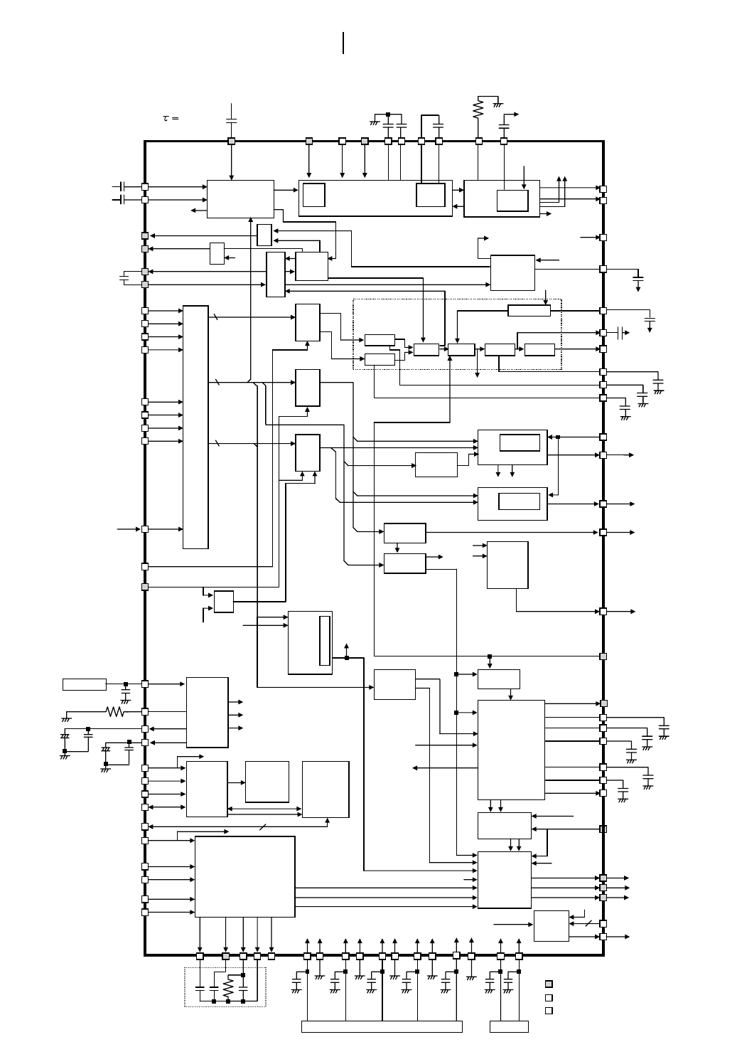
Block Diagram
56
RFIP
RFIN
Pick
I/F
0.068u
0.068u
IDGATE
TISH1
AGFU
AGFR
EQ-
AUTO
RF
LPP
Wobble F0-CNT
AGC3BPFSUB
AGC1
DPD
TE BALANCE
FE
FE
RECD
SAV
MIRR
DEFECT
TIE
R-OPC
OPC
APC
Serial
Cont.
Reg.
VREF
Power
Cont.
Programm
able I/O
port
SIGM
PE
HFSUM
BALANCE
AGC2 COMP
EQ
HP3
RF
AGC
HP2
ID
DET
S/H
S/H
S/H
WRF
MUX
RF SLIM/SUB
(RGA)
M
U
X
M
U
X
M
U
X
M
U
X
AGHPF2
RFHLD/
SPDSH
LO_ZB/
IREFE
EQFCF
EQOP
EQON
MA
MB
MC
MD
SA
SB
SC
SD
HAVC
MPDSH/
WOB
main
sub
4
4
2
SUBO/LPPMON
SUBI/LPPSIG
BHC
IP1/LPPOUT
D
WOBSIG
WAG3
WAG1
WAG2
WBLSH
MCLK
TE
FE
PE
HFPE
mclk
IREFT
RRF
WRF
BLANK
TOPH
BOTH
DFT
RECD
SPBLVL/TISH2
PHBETA/TCE
BHBETA/TIE
MRSTB
SDEN
SCLK
SDATA
BCENT
SPBLVL
SIGM
each blocks
WGATE
WGATE
RFPDSH
FMD
FVREF
PWRMON
VRDCN
VRDC
LDOUT
BHOUT
0.068u
0.033u
0.12U
0.12U
0.1U
12k
(*2)
3300p 0.1u
0.47u
D
D
D
LO_ZB/SPDSH
pin
D
D
D
D
D
D
D
D
D
D
D/A
D
SUBP.N
IP2/MIRR
D
SUBW
BPO
to MIRR.DEFECT
EQOP/N
BPO
2200p
SPDSH
RFHLD/TISH1 pin
VRDC2N/
RFHLD/TISH1 pin
GND2
VDD1
GND3
VDD2
GND4
VDD3
GND5
VDD4
VDD5
GND1
vCC2
DDD
VREF1
...Combined pin
...digital pin
D
...digital/analog pin
D/A
power 5V
power 3.3V(VDD)
4700p
15,000p
VREF1
GCAOUT
MIRRTOPH
MIRRBOTH
MIRRHPF
pick-up I/F
reference level
AWOBSIG
WOBFCF
VREF1
LO_ZB/SPDSH
PWWMON
D
LNDTRK
mclk
mclk
mclk
SHPE
ATEST
SUMF/
SUMF2
8200p
680k
3.3u
*3300P/0.068u
0.47u
0.1u 0.033u
0.033u
(*1), (*2)...1% Resistor
toLPF,A/D
toLPF,A/D
toLPF,A/D
toLPF,A/D
toLPF,A/D
toLPF,A/D
to LPF,A/D
*HPF fc=1kHz
to A/D
*3300p
Lo-Z function by IDGATE.
fast mode 3.3us
Lo-Z function by IDGATE.
0.1u
20k(*1)
LPPMON/EQOS/RRF/WRF
EQOS
VFREFO
10u
VREF1
SRVREF
power 3.3V
VHALH(=VDD/2)
VREF1(=2.1V)
FVREFO(=2.5V)
MPP SPP
to LE
MPP
SPP
SUMF2
to WRF
SUMF2
In the case of
analog APC
vCC1
LE toLPF,A/D
IP2/MIRR pin
MIRR
MIRR
AGHPF1
0.1u
0.1u
0.1u
0.1u
0.1u
0.1u
0.1u
0.1u
0.01u
0.01u
PORT00~07.10~13
D
12
AIN1~3
3
VRDC3N
..

57
•Pin Functions
pin Name pin No. Type max. voltage Function
TE 1 Analog-Output Tracking error output terminal
FE 2 Analog-Output Focus error output terimnal
PE 3 Analog-Output PE output terminal
LE 4 Analog-Output Lens error output terminal
BCENT 5 Analog-Output OPC center signal output terminal
PHBETA/TCE 6 Analog-Output OPC top hold level signal and APC write sampleing
signal output terminal/tilt servo detecting output terminal
BHBETA/TIE 7 Analog-Output OPC bottom hold level signal and R-OPC sampleing
signal output terminal/tilt servo detecting output terminal
VCC2 8 Power Power supply connected terminal(5V)
FVREF 9 Analog-Input VDD Reference voltage for APC input terminal
FMD 10 Analog-Input VDD APC monitor diode input terminal
VDD3 11 Power Power supply connected terminal(3.3V)
LDOUT 12 Analog-Output Terminal to control laser drivers for APC read system
VRDC3N 13 External-components required Terminal to connect laser driver control filters for APC
read
VRDC2N/PWRMON 14 External-components required Terminal to connect laser driver control filters for APC
read/ SH monitor output terminal
VRDCN 15 External-components required Terminal to connect laser driver control filters for APC
read
VRDC 16 External-components required Terminal to connect laser driver control filters for APC
read
GND3 17 Ground Ground connected terminal
WAG1 18 External-capacitor required Terminal to connect WOBBLE AGC detector capacitor
WAG2 19 External-capacitor required
WAG3 20 External-capacitor required
WOBFCF 21 External-capacitor required WOB-BPF f0 auto-adjustment external capacitor
connected terminal
VDD5 22 Power Power supply connected terminal(3.3V)
ATEST 23 Analog-Output Renesas analog test signal output terminal
AWOBSIG 24 Analog-Output Analog-level WOBBLE signal output terminal
GND5 25 Ground Ground connected terminal
LNDTRK 26 Digital-Inputpull-up VDD Balans adjustment mode selection
SPBLVL/TISH2 27 Digital-Inputpull-up VDD R-OPC WRF signal sampling pulse input terminal
/Tilt servo detecting sampling pulse input terminal
RFPDSH 28 Digital-Input putpull-up VDD APC read system sampling pulse input terminal
WFPDSH 29 Digital-Input putpull-up VDD APC write system sampling pulse input terminal
MPDSH/SPDSH 30 Digital-Input putpull-up VDD Pickup input sampling pulse input terminal
WBLSH 31 Digital-Input putpull-up VDD WOBBLE sampling pulse input terminal
WGATE 32 Digital-Input putpull-up VDD Read/write control input terminal
RFHLD/TISH1 33 Digital-Input putpull-up VDD RF hold control signal input terminal /Tilt servo detecting
sampling pulse input terminal
IDGATE 34 Digital-Input putpull-up VDD ID select pulse input terminal
LO_ZB/SPDSH 35 Digital-Input putpull-up VDD Low-z (reversal) pulse input terminal
/Pickup input sampling pulse input terminal

58
pin Name pin No. Type max. voltage Function
BLANK 36 Digital-Output Record/non-record detecting/BD detecting output
terminal
WOBSIG 37 Digital-Output WOBBLE signal output terminal
IP2/MIRR 38 Digital-Output ID detection/Mirror detection output terminal
IP1/LPPOUT 39 Digital-Output ID detection/LPP detection output terminal
DFT 40 Digital-Output Defect detection output terminal
GND4 41 Ground Ground connected terminal (Digital)
PORT00 42 Digital-Input/Output VDD I/O Port
PORT01 43 default input mode
PORT02 44 No pull-up
PORT03 45
PORT04 46
PORT05 47
PORT06 48
PORT07 49
MCLK 50 Digital/Analog-Input VDD Main clock input terminal
No pull-up Equalizer fc auto-adjustment control clock input terminal.
LPP output pulse width control clock input terminal.
WOB-BPF f0 auto-tracking clock input terminal.
PORT10 51 Digital-Input/Output VDD I/O Port
PORT11 52 default input mode
PORT12 53 No pull-up
PORT13 54
SCLK 55 Digital-Input pull-up VDD Serial I/F clock input terminal
SDATA 56 Digital-Input/Output pull-up VDD Serial I/F data input/output terminal
SDEN 57 Digital-Input pull-up VDD Serial I/F enable input terminal
MRSTB 58 Digital-Input pull-up VDD Master reset (reversal) input terminal
VDD4 59 Power Power supply connected terminal(3.3V)(digital)
BHC 60 External-capacitor required External capacitor for LPP bottom hold terminal
MIRRHPF 61 External-capacitor required Terminal to connect Mirror envelope detector HPF
capacitor
MIRRBOTH 62 External-capacitor required Terminal to connect Mirror envelope detector bottom
hold capacitor
MIRRTOPH 63 External-capacitor required Terminal to connect Mirror envelope detector top hold
capacitor
BOTH 64 External-capacitor required Terminal to connect envelope bottom hold capacitor
TOPH 65 External-capacitor required Terminal to connect envelope top hold capacitor
GND1 66 Ground Ground connected terminal
EQOP 67 Differential-Output RF equalizer differential output terminal
EQON 68
VDD1 69 Power Power supply connected terminal(3.3V)
SUBI/LPPSIG 70 Analog-Input VDD ID detecting HPF input terminal/LPP detecting HPF input
terminal

59
pin Name pin No. Type max. voltage Function
SUBO/LPPMON 71 Analog-Output ID detecting HPF output terminal/LPP detecting HPF
output terminal
EQFCF 72 External-capacitor required Terminal to connect RF-equalizer fc auto-adjustment
external capacitor
IREFE 73 External-resistor required Terminal to connect RF-equalizer fc setting external
resistor
AGHPF2 74 External-capacitor required Terminal to connect AGC high pass filter capacitor
AGHPF1 75
AGFU 76 External-capacitor required AGC filter connecting terminal
AGFR 77 External-capacitor required
VCC1 78 Power Power supply connected terminal(5V)
SUMF/SUMF2 79 Analog-Input/ /External-capacitor required VDD SUM RF input/SUM differential amp. DC filter
connected terminal
RFIP 80 Differential-Input VDD RF differential input terminal
RFIN 81
SRVREF 82 Analog-Input VDD DSP supply voltage (3.3V) input terminal
FVREFO 83 Analog-Output 2.5V reference bias voltage output terminal
IREFT 84 External-resistor required Terminal to connect reference current setting external
resistor
VREF1 85 Analog-Output 2.1V reference bias voltage output terminal
HAVC 86 Analog-Input VCC Pickup reference voltage input terminal
SA 87 Analog-Input VCC Sub beam 4D input terminal
SB 88 Analog-Input
SC 89 Analog-Input
SD 90 Analog-Input
VDD2 91 Power Power supply connected terminal(3.3V)
MA 92 Analog-Input VCC Main beam 4D input terminal
MB 93 Analog-Input
MC 94 Analog-Input
MD 95 Analog-Input
GND2 96 Ground Ground connected terminal
AIN1 97 Analog-Input VDD Analog input terminal
AIN2 98 Analog-Input
AIN3 99 Analog-Input
SIGM 100 Analog-Output Analog signal monitoring output terminal

60
IC301 (R8J32007FPV) : Encoder, Decoder & DSP Singal Processor
1.1 Pin Layout
CPU15
A17
EFG
SFG
TLD
SPD
LDD
LE D
GPIO04
ICUIN8
ICUIN6
ICUIN7
TESTB1
TESTB2
MRSTB
VSSIO
VCCIO
VCC
PTEST3
VDDAA
PTEST2
VSSA
REXT
VDDAA
PTEST1
VSSA
VINP
VDDAA
VINN
VSSA
VCCA
VCCA
DAVC
TVDN
TVDP
TRD
FOD
GAD1
GAD0
BCENT
TIB H
TCPH
LPSA
TE
ATZC
SIGM
PE
FE
VSSA
VSSA
VCCA
W1LPF0
W1LPF1
W1LPF2
216
215
214
213
212
211
210
209
208
207
206
205
204
203
202
201
200
199
198
197
196
195
194
193
192
191
190
189
188
187
186
185
184
183
182
181
180
179
178
177
176
175
174
173
172
171
170
169
168
167
166
165
164
163
V
SSR 1 162 W2LPF0
V
CCR 2 161 W2LPF1
CPU14 3 160 W2LPF2
CPU13 4 159
V
DDA
A
CPU12 5 158
V
SSA
A
V
SSIO 6 157 DEFECT
V
CCIO 7 156 BL AN
K
V
CCR
Q
8155 LN DTR
K
CPU11 9 154 WOBSIG
CPU10 10 153 LOWZB
V
SSR
Q
11 152 ID GATE
CPU9 12 151 RFHLD
CPU8 13 150 IP1LP PIN
CPRDB 14 149 IP2M IRR
UCS0B 15 148
V
CCIO
A1 16 147
V
SSIO
CPU0 17 146
V
DD
CPU1 18 145
V
SS
CPU2 19 144
V
SS
A
CPU3 20 143 NRZI
CPU4 21 142 NRZIB
V
SSR
Q
22 141 DCLKB
CPU5 23 140 DCL
K
CPU6 24 139
V
CC
A
CPU7 25 138 WRGATEB
V
CCR
Q
26 137 SRFH
V
SS 27 136 SRFL
V
DD 28 135 WRSTOP
A16 29 134 WRGATE2
A15 30 133
V
CCIO
V
SSIO 31 132
V
SSIO
V
CCIO 32 131
V
SS
A14 33 130
V
DD
A13 34 129 WBLSH
A12 35 128 MPDSH
A11 36 127 WFPDSH
A10 37 126 RFPDSH
A9 38 125 TCSHSPBLV
A20 39 124 LDB USY
CPWRB 40 123 WDEN
V
DD 41 122 RFDEN
V
SS 42 121 SDAT
A
A19 43 120 SCL
K
A18 44 119 FEMC
K
A8 45 118 TRST
A7 46 117 TDO
A6 47 116 TDI
A5 48 115 TC
K
A4 49 114 TMS
A3 50 113 TEST3
V
SSIO 51 112 TEST2
V
CCIO 52 111 TEST1
V
CCR 53 110 TEST0
V
SSR 54 109 DOUT
55
56
57
58
59
60
61
62
63
64
65
66
67
68
69
70
71
72
73
74
75
76
77
78
79
80
81
82
83
84
85
86
87
88
89
90
91
92
93
94
95
96
97
98
99
100
101
102
103
104
105
106
107
108
A2
GPIO05
VSSIO
VCCIO
HRSTB
DATA7
DATA8
DATA6
DATA9
DATA5
DAT A10
DATA4
DAT A11
DATA3
DAT A12
DATA2
DAT A13
VDD
VSS
VSSIO
VCCIO
DATA1
DAT A14
DATA0
DAT A15
DREQ
ZIOWB
ZIORB
IORDY
DACKB
HIN TRQ
IOCS16B
VSSIO
VCCIO
DA1
PDIA GB
DA0
DA2
CS1FXB
CS3FXB
DASPB
GPIO07
GPIO06
ROUT
VCCA
LOU T
ADIP VR1
ADIP VRT
ADIPINP
VSSA
VSSA
XCO
XCI
VCCA
R8J32007
Top View
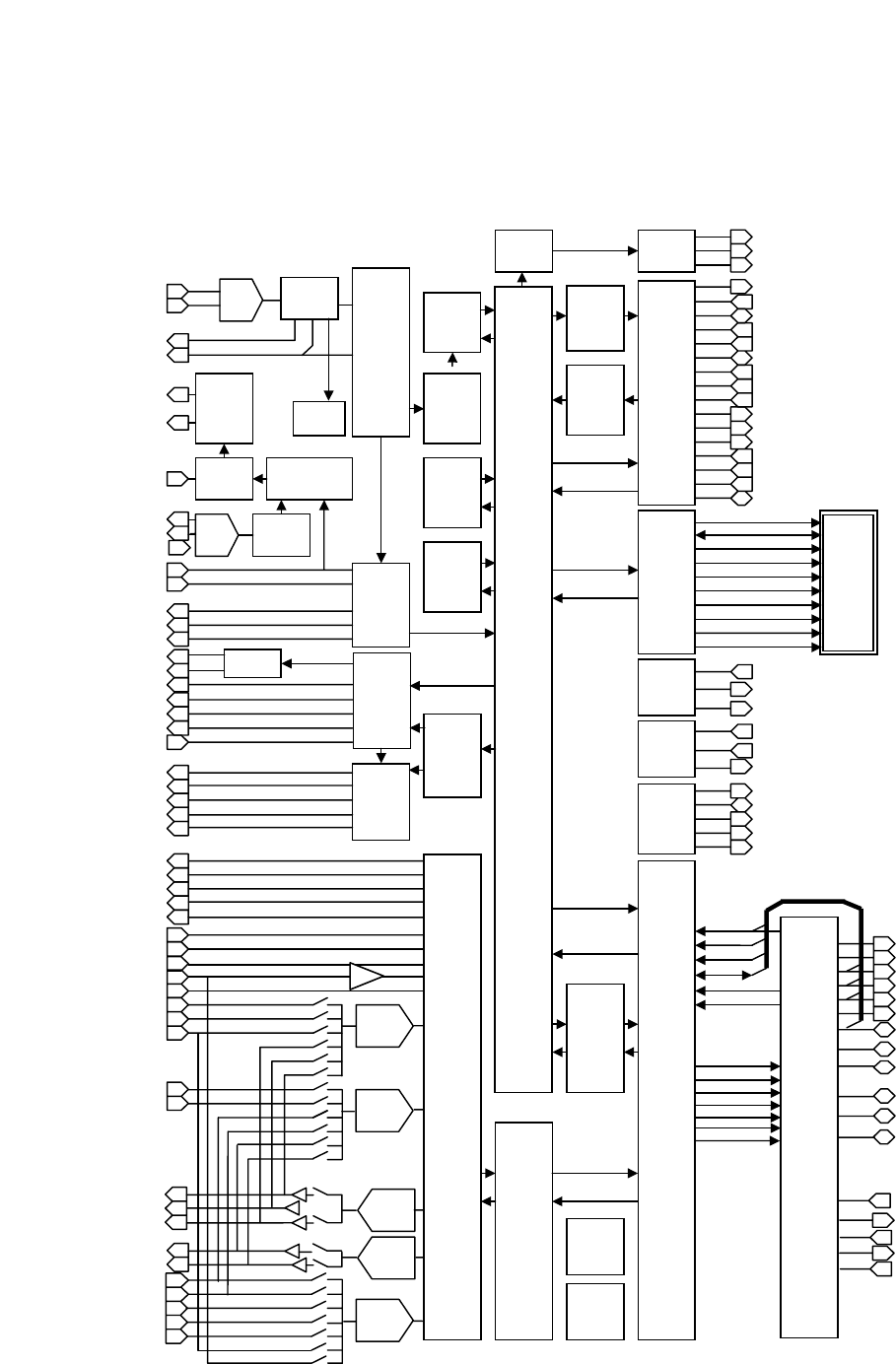
1.2 Block Diagram
61
Data
WPLL
ADIP
Detector
Detector
Counter
PRML
PLL
Generator
Demodulate
Servo
CD-ROM
Decoder
DVD
PI-ECU
DVD
PO-ECU
DRAM
MCIF
ATAPI
AUDIO
DRAM
Interface
Clock
Generator
Test
Control
VINP
VINN
REXT
PTEST [2:0]
IP1LPPIN
IP2MIRR
LOWZB
IDGATE
RFHLD
W1LPF[2:0]
ADC
ADC
ADIPVRT
LPP
Wobble
WOBSIG
Jitter CD-DSP
CAV
AUDIO
NRZI,NRZIB LVDS
DCLK,DCLKB
WGATEB
WRGATE2
SRFH
WRSTOP
Sample
Hold
WBLSH
MPDSH
WFPDSH
RFPDSH
CD-ROM
CD
Encoder
Modulator
DAC
ADC
FE
PE
TE
LPSA
FOD
DAVC
TRD
XCI
TRST(NMI)
TCK(SCK)
TDI(SCI)
TDO(SCO)
TMS
XCO
Serial I/F
SDATA
RFDEN
SCLK
WDEN
LDBUSY
FEMCK
TEST[3:0]
MRSTB
TESTB[1:2]
ROUT
DOUT
LOUT
DVD
Descramble
DVD
Scramble
Auth
BCA
SSEQ
MSEQ
RA[12.10:0]
DWE
RD[15:0]
DRAS
DCAS
RAMCL
DQMU
DQML
DACKB
CS3FXB
DREQ
CS1FXB
PDIAGB
DASPB
DA2
IOCS16B
IORDY
ZIOWB
HINTRQ
HRSTB
ZIORB
DATA [15:0]
DA1
DA0
SFG
ATZC
DERECT
BLANK
EFG
LED
LNDTRK
LDD
TLD
TCSHSPBLV
DCKE
W2LPF[2:0]
H8S
CPU
ADC
GAD1
ADGATEB
INT0B
FOK
CPWRB
CPRDB
UCS2B
A[20:0]
CPU[15:0]
INT1B
INT2B
UCS0B
GPIO05(UCS1B)
CPRDB
CPWRB
A[20:1]
CPU[15:0]
GPIO06(CSEL)
GPIO07(HEATRUN)
ICUIN6(EJECTSW)
ICUIN7(ACTFLG)
GPIO04(A[0])
SDRAM
16Mbit
ZCS
UCS3B
INT3B
SRFL
TCPH
TIBH
BCENT
FAD0(VRDC2N)
TVDP
TVDN
ADC
WAI T
ICUIN8(LOADIN)
DAC
SIGM
SPD
ADIPINP
ADIPVR1
Cmp

62
1.3 Pin Table
Pin no Pin Name
1 VSSR
2 VCCR
3 CPU14
4 CPU13
5 CPU12
6 VSSIO
7 VCCIO
8 VCCRQ
9 CPU11
10 CPU10
11 VSSRQ
12 CPU9
13 CPU8
14 CPRDB
15 USC0B
16 A1
17 CPU0
18 CPU1
19 CPU2
20 CPU3
21 CPU4
22 VSSRQ
23 CPU5
24 CPU6
25 CPU7
26 VCCRQ
27 VSS
28 VDD
29 A16
30 A15
31 VSSIO
32 VCCIO
33 A14
34 A13
35 A12
36 A11
37 A10
38 A9
39 A20
40 CPWRB
41 VDD
42 VSS
43 A19
44 A18
45 A8
46 A7
47 A6
48 A5
49 A4
50 A3
51 VSSIO
52 VCCIO
53 VCCR
54 VSSR
Pin no Pin Name
55 A2
56 GPIO05
57 VSSIO
58 VCCIO
59 HRSTB
60 DATA7
61 DATA8
62 DATA6
63 DATA9
64 DATA5
65 DATA10
66 DATA4
67 DATA11
68 DATA3
69 DATA12
70 DATA2
71 DATA13
72 VDD
73 VSS
74 VSSIO
75 VCCIO
76 DATA1
77 DATA14
78 DATA0
79 DATA15
80 DREQ
81 ZIOWB
82 ZIORB
83 IORDY
84 DACKB
85 HINTRQ
86 IOCS16B
87 VSSIO
88 VCCIO
89 DA1
90 PDIAGB
91 DA0
92 DA2
93 CS1FXB
94 CS3FXB
95 DASPB
96 CPIO07
97 CPIO06
98 ROUT
99 VCCA
100 LOUT
101 ADIPVR1
102 ADIPVRT
103 ADIPINP
104 VSSA
105 VSSA
106 XCO
107 XCI
108 VCCA
Pin no Pin Name
109 DOUT
110 TEST0
111 TEST1
112 TEST2
113 TEST3
114 TMS
115 TCK
116 TDI
117 TDO
118 TRST
119 FEMCK
120 SCLK
121 SDATA
122 RFDEN
123 WDEN
124 LDBUSY
125 TCSHSPBLV
126 RFPDSH
127 WFPDSH
128 MPDSH
129 WBLSH
130 VDD
131 VSS
132 VSSIO
133 VCCIO
134 WRGATE2
135 WRSTOP
136 SRFL
137 SRFH
138 WRGATEB
139 VCCA
140 DCLK
141 DCLKB
142 NRZIB
143 NRZI
144 VSSA
145 VSS
146 VDD
147 VSSIO
148 VCCIO
149 IP2MIRR
150 IP1LPPIN
151 RFHLD
152 IDGATE
153 LOWZB
154 WOBSIG
155 LNDTRK
156 BLANK
157 DEFECT
158 VSSAA
159 VDDAA
160 W2LPF2
161 W2LPF1
162 W2LPF0
Pin no Pin Name
163 W1LPF2
164 W1LPF1
165 W1LPF0
166 VCCA
167 VSSA
168 VSSA
169 FE
170 PE
171 SIGM
172 ATZC
173 TE
174 LPSA
175 TCPH
176 TIBH
177 BCENT
178 GAD0
179 GAD1
180 FOD
181 TRD
182 TVDP
183 TVDN
184 DAVC
185 VCCA
186 VCCA
187 VSSA
188 VINN
189 VDDAA
190 VINP
191 VSSA
192 PTEST1
193 VDDAA
194 REXT
195 VSSA
196 PTEST2
197 VDDAA
198 PTEST3
199 VCC
200 VCCIO
201 VSSIO
202 MRSTB
203 TESTB2
204 TESTB1
205 ICUIN7
206 ICUIN6
207 ICUIN8
208 GPIO04
209 LED
210 LDD
211 SPD
212 TLD
213 SFG
214 EFG
215 A17
216 CPU15

63
1.4 Pin Functions
It corresponds to the following signs as a pin I/O specification.
AI : Analog Input
AO : Analog Output
AIO : Analog Input/Output
I : Standard Input
IU : Standard Input with Pull Up
O : Standard Output
TO : Standard Three State Output
IO : Standard Input/Output
IOU : Standard Input/Output with Pull Up
5I : 5V Tolerant Input
5O : 5V Tolerant Output
5TO : 5V Tolerant Three State Output
5IO : 5V Tolerant Input/Output
PW : Power Supply Pin
GND : Earth Pin
Data PLL/PRML Pin List
Pin Name Pin No. I/O destination Function
VINP 190 AI AFE RF signal normal phase input pin
VINN 188 RF signal counter phase input pin
REXT 194 AO External Resistance Resistor connect pin for reference current generation
PTEST1 192 AO External Resistance PRML/Data PLL moniter D/A output pin
PTEST2 196 PRML/Data PLL moniter D/A output pin
PTEST3 198 Data PLL VCO control voltage monitor pin
Wpll Pin List
Pin Name Pin No. I/O destination Function
W1LPF0 165 AO External Components Write PLL1 filter connect pin (0)
W1LPF1 164 Write PLL1 filter connect pin (1)
W1LPF2 163 Write PLL1 filter connect pin (2)
W2LPF0 162 AO External Components Write PLL2 filter connect pin (0)
W2LPF1 161 Write PLL2 filter connect pin (1)
W2LPF2 160 Write PLL2 filter connect pin (2)

64
Servo Pin List
Pin Name Pin No. I/O destination Function
BLANK 156 I AFE Blank signal input
(also connected to the H8S interrupt port INT5)
DEFECT 157 I AFE Defect (scratch detect) signal
SFG 213 IU DRVR Spindle FG pulse
(also input to the H8S interrupt port INT4)
EFG 214 I PU Spindle FG pulse for Light Scribe
(also input to the H8S interrupt port INT4)
TLD 212 TO DRVR Tilt drive signal (PWM output)
SPD 211 TO DRVR Spindle drive signal (PWM output)
LDD 210 TO DRVR Loading drive signal (PWM output)
LED 209 TO PU LPS_LED control signal (PWM output)
ATZC 172 AI AFE Tracking Zero Cross input signal
FE 169 AI AFE Focus error: sampled at 352.8 kHz
PE 170 AI AFE Laser power error: sampled at 352.8 kHz
SIGM 171 AI AFE Signal monitor: sampled at 88.2/176.4 kHz
TE 173 AI AFE Tracking error: sampled at 352.8 kHz
LPSA 174 AI AFE Lens positioning/lens error: sampled at 88.2 kHz
TCPH 175 AI AFE Tracking center/BETA top hold: sampled at 44.1/176.4 kHz
TIBH 176 AI AFE Tilt error/BETA bottom hold: sampled at 44.1/176.4 kHz
BCENT 177 AI AFE BETA center: sampled at 176.4 kHz
GAD1 179 AI General AD input: sampled at 88.2 kHz
GAD0(VRDC2N) 178 AI General AD input: sampled at 176.4 kHz
FOD 180 AO DRVR Focus control signal
TRD 181 AO DRVR Tracking control signal
TVDP 182 AO DRVR Sled drive signal (normal phase)
TVDN 183 Sled drive signal (counter phase)
DAVC 184 AO DRVR Servo system Vcc/2 voltage output pin

65
ATAPI Interface Pin List
Pin Name Pin No. I/O destination Function
HRSTB 59 5I ATAPI ATAPI-IF control signal (host reset signal)
DA2 92 5I ATAPI ATAPI-IF register address signal
DA1 89
DA0 91
DATA[15:0] 79,77,71, 5IO ATAPI ATAPI- IF data bus
69,67,65,
63,61,60,
62,64,66,
68,70,76,
78
DREQ 80 5TO ATAPI ATAPI-IF DMA request signal
ZIOWB 81 5I ATAPI ATAPI-IF write strobe pulse
ZIORB 82 5I ATAPI ATAPI-IF read strobe pulse
IORDY 83 5TO ATAPI ATAPI-IF control signal (drive Ready)
DACKB 84 5I ATAPI ATAPI-IF DMA acknowledge
HINTRQ 85 5TO ATAPI ATAPI-IF drive interrupt signal
IOCS16B 86 5TO ATAPI ATAPI-IF control signal (16-bit transfer)
PDIAGB 90 5IO ATAPI ATAPI-IF control signal
CS1FXB 93 5I ATAPI ATAPI-IF register chip select signal
CS3FXB 94
DASPB 95 5IO ATAPI ATAPI-IF control signal

66
Encoder Interface Pin List
Serial Communication Interface Pin List
Pin Name Pin No. I/O destination Function
IP1LPPIN 150 I AFE PID area identification signal/LPP input signal
IP2MIRR 149 I AFE PID area identification signal/MIRR signal
WOBSIG 154 I AFE Wobble signal input
LOWZB 153 O AFE Input impedance switch control signal/SPDSH; running
OPC sampling pulse (Pit top)
IDGATE 152 O AFE ID/data switch signal
RFHLD 151 O AFE VFO3 holding signal and track center signal sample &
hold signal
WRGATE2 134 O AFE Write gate signal output
WBLSH 129 O AFE Wobble signal sampling pulse
MPDSH 128 O AFE Main beam sampling pulse
WFPDSH 127 O AFE Laser control sampling pulse
(Front monitor write/erase block)
RFPDSH 126 O AFE Laser control sampling pulse
(Front monitor read block)
TCSHSPBLV 125 O AFE VFO1 track center signal sample & hold pulse;
/SPBLVL running OPC sampling pulse (Pit end)
WRGATEB 138 O PU Write gate signal
SRFH 137 O PU I- V amplifier gain switch (HI side)
/I- V amplifier gain switch (for binary)
SRFL 136 I- V amplifier gain switch (Low side)
WRSTOP 135 I PU Write stop gate signal
LNDTRK 155 O AFE/PU Land/groove switch
NRZI 143 AO PU NRZI output after modulation (normal phase)
NRZIB 142 NRZI output after modulation (counter phase)
DCLK 140 AO PU NRZI sync clock (counter phase)
DCLKB 141 NRZI sync clock (normal phase)
ADIPVR1 101 AO External Cpmponents AD related pin for ADIP detection
ADIPVRT 102 AO External Cpmponents AD related pin for ADIP detection
ADIPINP 103 AI AFE ADIP detect input pin
Pin Name Pin No. I/O destination Function
LDBUSY 124 IO LDD LDD serial IF busy also functions as the CPU general port 1-0
WDEN 123 O LDD LDD microcomputer I/F (transfer enable signal)
RFDEN 122 O AFE AFE microcomputer I/F (transfer enablesignal)
SDATA 121 IO AFE/LDD AFE/LDD microcomputer I/F (transfer data signal 3Vsystem)
SCLK 120 O AFE/LDD AFE/LDD microcomputer I/F (transfer clock signal)

67
Audio Interface Pin List
Pin Name Pin No. I/O destination Function
DOUT 109 IO ATAPI Digital output pin,also functions as the CPU general port 1-2
ROUT 98 AO ATAPI Audio Lch & Rch output
LOUT 100
Clock Generator Pin List
Pin Name Pin No. I/O destination Function
FEMCK 119 O AFE Front End LSI clock
XCO 106 O X’tal Crystal oscillation 33.8688MHz
XCI 107 I X’tal Crystal oscillation 33.8688MHz
Flash/SRAM Pin List
Pin Name Pin No. I/O destination Function
UCS0B 15 O Flash H8S / CS0
CPWRB 40 O Flash / SRAM H8S / WRB
CPRDB 14 O Flash / SRAM H8S / RDB
A[20:1] 39,43,44, O Flash / SRAM H8S / A[20:1]
215,29,30,
33,34,35,
36,37,38,
45,46,47,
48,49,50,
55,16
CPU[15:1] 216,3,4, IO Flash / SRAM H8S / D[15:0]
5,9,10, CPU[0] can also function as the CPU general port 0-4
(multiplexed).
12,13,25,
24,23,21,
20,19,18
17
H8S Micro-Processor Pin List
CPU
Pin Name Pin No. I/O destination Function
ICUIN7(ACTFLG) 205 IU DRVR CPU interrupt port INT7: Pick up protect flag
ICUIN6(EJECTSW) 206 I Eject Switch CPU interrupt port INT6: EJECTSW interrupt request
ICUIN8(LOADIN) 207 IO Load Switch CPU general port1-1 also connected to the CPU interrupt
port INT8: Loader in sensor
GPIO07(HEATRUN) 96 5IO ATAPI CPU general port 0-7 :Off heat run test input
GPIO06(CSEL) 97 5IO ATAPI CPU general port 0-6 ATAPI CSEL
GPIO04(A0) 208 IO SRAM CPU general port 0-4, also functions as H8S / A0
GPIO05(UCS1B) 56 IO SRAM CPU general port 0-5, also functions as H8S / CS1

68
LSI/TEST Control Pin List
Pin Name Pin No. I/O destination Function
MRSTB 202 I RESET IC Master reset input
TESTB2 203 I Test select
TESTB1 204
TMS 114 IU E10emulator Test data switch for E10emulator
TCK 115 IOU E10emulator Test clock for E10 emulator
It can function as a SCI serial clock output port when E10
emulator is not used (multiplexed).
TDI 116 IU E10emulator Test data input for E10 emulator
It can function as a SCI serial data input port when E10
emulator is not used (multiplexed).
TDO 117 O E10emulator Test data output for E10 emulator
It can function as a SCI serial data output port when E10
emulator is not used (multiplexed).
TRST 118 I E10emulator Test reset for E10 emulator
/Non-mask CPU interrupt port(falling edge sense)
TEST0 110 IO User test/CPU general port2
TEST1 111 Test monitor can be set as the following table by a register
TEST2 112
TEST3 113
T*SEL[3:0] TEST0 TEST1 TEST2 TEST3
0 Servo monitor 0 Servo monitor 1 Servo monitor 2 Servo monitor 3
1 WPLL monitor 0 WPLL monitor 1 WPLL monitor 2 WPLL monitor 3
2 Audio 0 Audio 1 Audio 2 Audio 3
3 DVD modulation 0 DVD modulation 1 DVD modulation 2 DVD modulation 0
4 DVD-R/CD-R DVD-R/CD-R DVD-R/CD-R DVD-R/CD-R
monitor 0 monitor1 monitor 2 monitor 3
5 DVD+RW monitor 0 DVD+RW monitor1 DVD+RW monitor 2 DVD+RW monitor 3
6 PI/C1 PI/C1 PI/C1 PI/C1
7 PO/C2 PO/C2 PO/C2 PO/C2
8 DEMO 0 DEMO 1 DEMO 2 DEMO 3
9- - - -
10 CLVCK CLVCK CLVCK CLVCK
11 BLEND BLEND BLEND BLEND
12 PRML monitor 0 PRML monitor 1 PRML monitor 2 PRML monitor 3
13 Data PLL monitor 0 Data PLL monitor 1 Data PLL monitor 2 Data PLL monitor 3
14 RAMCON monitor 0 RAMCON monitor 1 RAMCOM monitor 2 RAMCON monitor 3
15 MIF monitor 0 MIF monitor 1 MIF monitor 2 MIF monitor 3
16 WOBREF monitor 0 WOBREF monitor 1 WOBREF monitor 2 WOBREF monitor 3
T*SEL can be set for each of pins TEST3, TEST2, TEST1, and TEST0, respectively.

69
Power Supply/GND Pin List
Pin Name Pin No. I/O Function
VDD 28,41,72, PW DSP core power supply (1.5V)
130,146
VCCR 2,53 PW SDRAM power supply (3.3V)
VCCRQ 8,26 SDRAM I/O power supply (3.3V)
VDDAA 159 PW 1.5V system analog power supply (1.5V) WPLL1,2
189,193,197 1.5V system analog power supply (1.5V) PRML A/D Data PLL
VCCA 99 PW Analog power supply (3.3V):AUDIO / ADIP
108 Analog power supply (3.3V):PLL multiplication
139 Analog power supply (3.3V):LVDS
166 Analog power supply (3.3V):WPLL1,2
185 Analog power supply (3.3V):Servo A/D D/A
186 Analog power supply (3.3V):PRML A/D Data PLL
VCC 199 PW Digital power supply (3.3V):PRML A/D Data PLL
VCCIO 7,32,52, PW DSP I/O power supply (3.3V)
58,75,88,
133,148,200
VSS 27,42,73, GND DSP core GND
131,145
VSSR 1,54 GND SDRAM GND
VSSRQ 11,22 GND SDRAM I/O GND
VSSA 104 GND Analog GND:AUDIO / ADIP
105 Analog GND:PLL multiplication
144 Analog GND:LVDS
167 Analog GND:WPLL1,2
168 Analog GND:Servo A/D D/A
187,191,195 Analog GND:PRML A/D Data PLL
VSSAA 158 GND 1.5V system analog GND:WPLL1,2
VSSIO 6,31,51, GND DSP I/O GND
57,74,87, Connected SDRAM I/O GND through 6,31pin
132,147,201
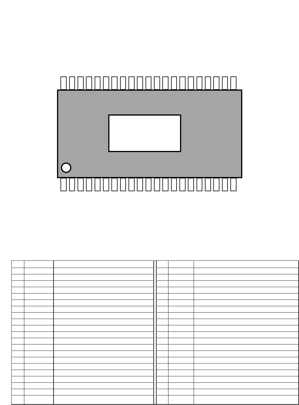
70
No Pin name Function
1 SPIN Spindle control voltage input
2 SL1IN Slide control voltage input1
3 SL2IN Slide control voltage input2
4 SPLIM Input terminal for spindle current limit
5 VM2 Motor Power Supply 2(for Slide)
6 SL2+ Slide non-inverted output2
7 GND GND
8 SL2- Slide inverted output2
9 SL1+ Slide non-inverted output1
10 SL1- Slide inverted outptut1
11 GND GND
12 U Motor drive output U
13 V Motor drive output V
14 W Motor drive output W
15 ACTFLG Pickup protect flag output
16 COMMON Motor common
17 TEST Test terminal (*1)
18 SLLIM Input terminal for slide current limit
19 FG Frequency generator output
20 EN1 Input terminal for enable 1
21 EN2 Input terminal for enable 2
No Pin name Function
42 REF Reference voltage input
41 LOIN Loading control input
40 FOIN Focus control voltage input
39 TOIN Tracking control voltage input
38 TLIN Tilt control voltage input
37 TL- Tilt inverted output
36 TL+ Tilt non-inverted output
35 FO- Focus inverted output
34 FO+ Focus non-inverted output
33 GND GND
32 5VCC 5V Power Supply (for FS,TS,TL)
31 TO+ Tracking non-inverted output
30 TO- Tracking inverted output
29 GND GND
28 LO- Loading inverted outptut
27 LO+ Loading non-inverted output
26 VM3 Power Supply3(for Loading)
25 ACTRST Pickup protect Reset (*2)
24 STTH Reference voltage for spindle start up
23 SPGS Input terminal for gain select SPM
22 VM1 Motor Power Supply 1(for Spindle)
Pin Function
*1) Please connect 17terninal (TEST) to GND or open, for TEST.
*2) Please connect 25terminal(ACTRST) to 5VCC, When the Pick-up protection circuit is not used.
IC601 (R2S30202FP) : SPINDLE MOTOR AND 6CH ACTUATOR DRIVER
Pin Layout
142SPIN REF
241SL1IN LOIN
340SL2IN FOIN
439SPLIM TOIN
538VM2 TLIN
637SL2+ TL-
736GND TL+
835SL2- FO-
934SL1+ FO+
10 33SL1- GND
11 32GND
R2S3
0202FP
5VCC
12 31U TO+
13 30V TO-
14 29W GND
15 28ACTFLG LO-
16 27COMMON LO+
17 26TEST VM3
18 25SLLIM ACTRST
19 24FG STTH
20 23EN1 SPGS
21 22EN2 VM1
Package outline : 42 PIN POWER SSOP (42P9R-K)
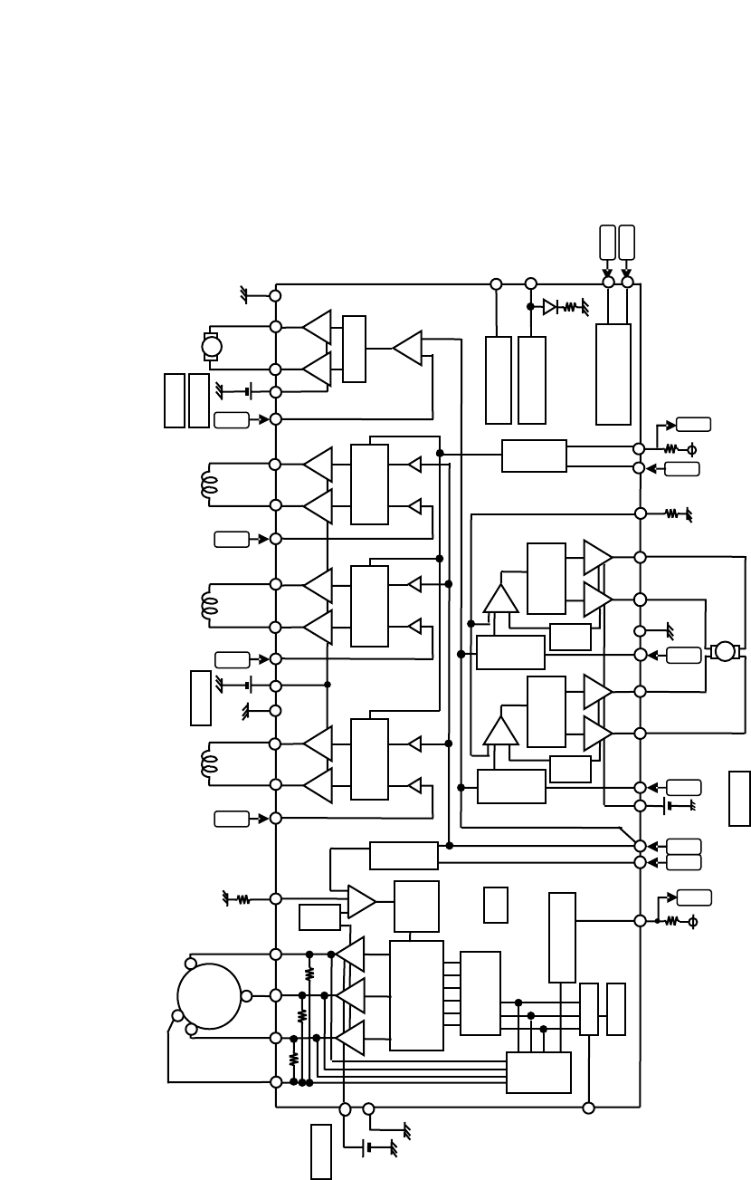
Block Diagram
71
STM
M
SWICHING
Commutation PWM
CIRCUIT
SPM
V/V converter
+-
CTL
SLIDE2
V/V converter
+
-
CTL
+
-
CTL
SL1+
SL1-
SL1IN
SL2+
SL2-
SL2IN
REF
SPIN
FG
U
V
W
FOIN
FO+
FO-
TRIN
TR+
TR-
VM2
SLIDE1
V/V converter
PWM
CIRCUIT PWM
CIRCUIT
Current
sense
Current
sense
Current
sense
GND
GND
DSP
DSP
DSP
DSP
DSP
DSP
DSP
BTLAMP
CurrentchopperPWM
Currentc
hopperPWM
SPLIM
DSP
5VCC
SLLIM
commutation
STARTER
CLK
TLIN
TL+
TL-
STTH
Current gain
0.88 A/V
BTLAMP
BTLAMP
OUTPUT Ron
1ohm
OUTPUT Ron
1.5ohm
OUTPUT Ron
1.5ohm
OUTPUT Ron
1.5ohm
OUTPUT Ron
1.8 ohm
6.4MHz
Frequency
75KHz Frequency
75KHz
Frequency
150KHz
Current gain
0.88 A/V
Current gain
3A/V
0.6A/V
OUTPUT Ron
1.8 ohm
For /FO/TR/TILT
VM1
GND
BACK EMF
DETECTER
TSD
SINCurrent chopperPWM
For SPINDLE
For SLIDE
7-13.2V
7-13.2V
4.5-5.5V
FG(x3)
Reverse detect
Voltage gain
x12 Voltage gain
x12 Voltage gain
x12
LO+
LO-
VM3
DSP
M
OUTPUT Ron
1.5ohm
GND
H Bridge
+ -
EN 1 DSP
EN 2 DSP
For LOADING
4.5-5.5V
7-13.2V
TEST
SPGS
Gain Select
(SPM)
ENABLE
COMMON
ACTRST
ACTFLG
DSP
DSP Pickup Protect
TEST mode
72
Input/Output circuit diagram
SPIN, SL1IN, SL2IN
LOIN
FOIN, TOIN,TLIN
TEST
REF EN1, EN2
SPGS ACTFLG,FG ACTRST
VM1, U, V, W VM2, SL1+, SL1-, SL2+, SL2-
5VCC, FO+, FO-, TO+, TO-, TL+, TL- VM3, LO+, LO-
5VCC 5VCC 5VCC 5VCC
5VCC 5VCC 5VCC
VM1 VM2
VM3
5VCC
U V W SL1+ SL1- SL2-SL2+
LO-LO+
FO-FO+ TO-TO+ TL-TL+
(Temperature monitor)
5VCC
5VCC
10k
25k
100 100
100 100 100 100
17k
35k
COMMON
VM1
U
COMMON 100
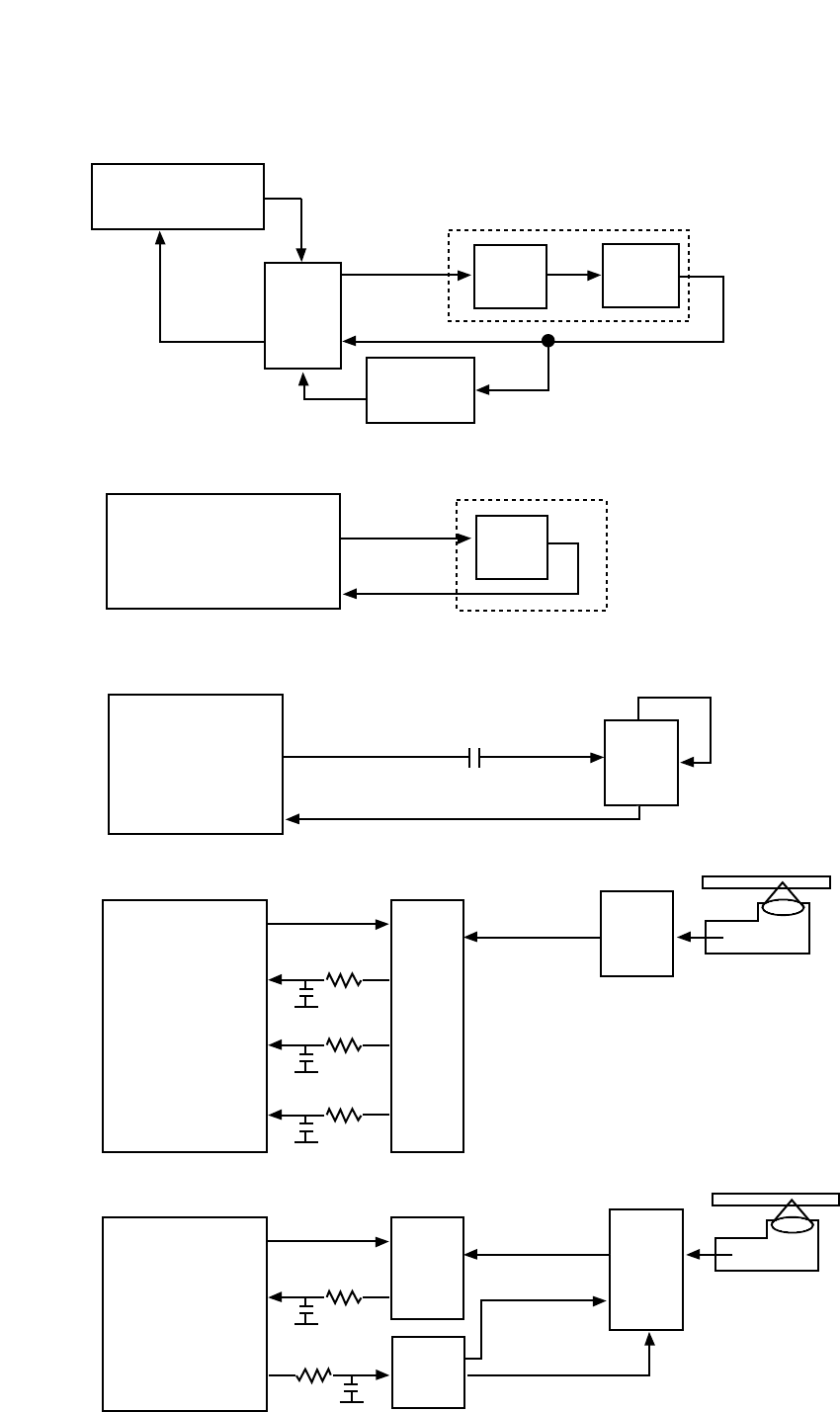
TROUBLESHOOTING GUIDE
73
MPU & DSP
IC301
MPU & DSP
IC301
MPU & DSP
IC301
AFE
IC101
AFE
IC101
Pickup
LD
Driver Front
Monitor
IC102
AFE
IC101
#6
Pin#79
Pin#110
Pin#203
Pin#
87-90
#2
#1
#3
C137 Pin#21
#10
#12
FFC
FFC
17,18,20,21
FFC
FFC
Pickup
Pickup
FFC
Setting
Setting
FE:R102,C405
Pin#175
pin#98
LD
Driver
TE:R101,C101
PE:R103,C406
(01) Laser Power Adjust (using RD Power/WR Power/Erase Power)
(02) High Frequency/NRZI skew Adjust
(03) Data Slice/Equalizer Boost/Raw Slice/ Equalizer Frequency Adjust
(04) Circuit Offset Adjust
(05) Focus Amp. Adjust for DVD-Dual
MPU & DSP
IC301
AFE
IC101
Driver
IC601
Pickup
Pin#
87-90
#2
#40
FFC
Slider FPC
Slider, #6,8-10
Focus:#34-35
DVD-Dual Disc
Setting
FE:R102,C405
R329,C335
MPU & DSP
IC301
74
MPU & DSP
IC301
AFE
IC101
Driver
IC601
Pickup
All Disc
Pin#
87-90
FFC
Setting
FE:R102,C405
Focus:#34-35
R329,
C335 #40
All Disc
MPU & DSP
IC301
AFE
IC101
Driver
IC601
Pickup
All Disc
Pin#
87-90
Setting
FE:R102,C405
Tracking:#30-31
Focus:#34-35
TE:R101,C101
R329,C335 #40
R330,C336 #39
MPU & DSP
IC301
AFE
IC101
Driver
IC601
Pickup
Pin#
87-90
#1
#2
PE:R103,C406
#3
#2
#1
FFC
Setting
TE:R101,C101
Tracking
#30-31
Slider FPC
Slider:#6,8-10
Slider FPC
Slider:#6,8-10
R330
C336
#39
(06) Focus Amp. and Total Amp. Adjust
(07) Tracking Amp. Adjust
(08) Servo Loop Gain Adjust
FFC
75
DVD-RAM Disc
MPU & DSP
IC301
AFE
IC101
Driver
IC601
Pickup
Pin#
80-81
#171 #100
FFC
Setting
SIGM:R148, C151
Slider FPC
Slider:#6, 8-10
DVD-RAM Disc
MPU & DSP
IC301
AFE
IC101
Driver
IC601
Pickup
Pin#
87-90,80-81
#67,68
FFC
Setting
C341,343
Slider FPC
Slider:#6, 8-10
DVD-RAM Disc
MPU & DSP
IC301
AFE
IC101
Driver
IC601
Pickup
Pin#
87-90,80-81
#100
FFC
Setting
SIGM:R148,C151
Slider FPC
Slider:#6, 8-10
(09) Unwritten Slice Level Adjust for DVD-RAM
(12) Focus Offset Adjust for DVD-RAM (Data Error pulse)
(11) Focus Offset Adjust for DVD-RAM (PID Amp)
DVD-ROM Disc
MPU & DSP
IC301
AFE
IC101
Driver
IC601
Pickup
Pin#
87-90,80-81
#2
FFC
Setting
FE:R102,C405
Slider FPC
Slider:#6, 8-10
(10) Focus Offset Adjust for DVD-ROM, CD-R/RW
76
Slider FPC
Slider:#6,8-10
MPU & DSP
IC301
AFE
IC101
Driver
IC601
Pickup
DVD-R/RW Disc
Pin#
87-90, 80-81
Pin#
87-90,80-81
FFC
Setting
TE:R101, C101
TRD:R330,C336
TILT: #36-37
#39
#181
#1
Tracking: #30-31
MPU & DSP
IC301
AFE
IC101
Driver
IC601
Pickup DVD-R/RW Disc
FFC
Setting
FE:R102, C405
FE:#34-35
FE
R329, C335 #40
#2
(14) Tilt Adjust for DVD-R/RW, DVD+R/RW, CD-R/RW
(15) Focus Deviation Adjust
Pin#
87-90,80-81
MPU & DSP
IC301
AFE
IC101
Driver
IC601
Pickup
DVD-R/RW Disc
FFC
Setting
TE:R101, C101
Tracking:#30-31
Slider FPC
Slider:#6, 8-10
R330, C336
TRD:
#39
#1
#181
(16) Focus Offset Adjust for DVD-R/RW, DVD+R/RW, CD-R/RW
MPU & DSP
IC301
AFE
IC101
Driver
IC601
Pickup DVD-RAM Disc
Pin#
87-90,80-81
FFC
Setting
TCE:R106, C106
Slider FPC
Slider:#6, 8-10
TIE:R107,C107
#6
#7
(13) Tilt Adjust for DVD-RAM
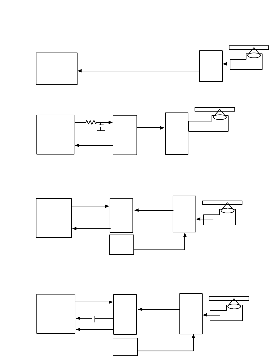
77
MPU & DSP
IC301
MPU & DSP
IC301
Driver
IC601
Pickup
FFC
FFC
(Temp.Information)
putemp
#178
Spindle
SPD:R349, C349
#211 #1 Pin#
12-14
#19
#213 FG
Pin#
87-90,80-81
MPU & DSP
IC301
AFE
IC101
Driver
IC601
Pickup
DVD+R Disc
FFC
Setting
WobSIG
Slider FPC
Slider:#6, 8-10
#154 #37
Pin#
87-90,80-81
MPU & DSP
IC301
AFE
IC101
Driver
IC601
Pickup
DVD-R/RW Disc
FFC
Setting
C341, 343
Slider FPC
Slider:#6,8-10
#67,68
#39
(17) Lens Sensitivity Adjust
(18) Spindle Offset Adjust
(19) ADIP BPF/Read Timing Adjust for DVD+R/RW
(20) Focus Offset Adjust for DVD-R/RW, DVD+R/RW(DID)
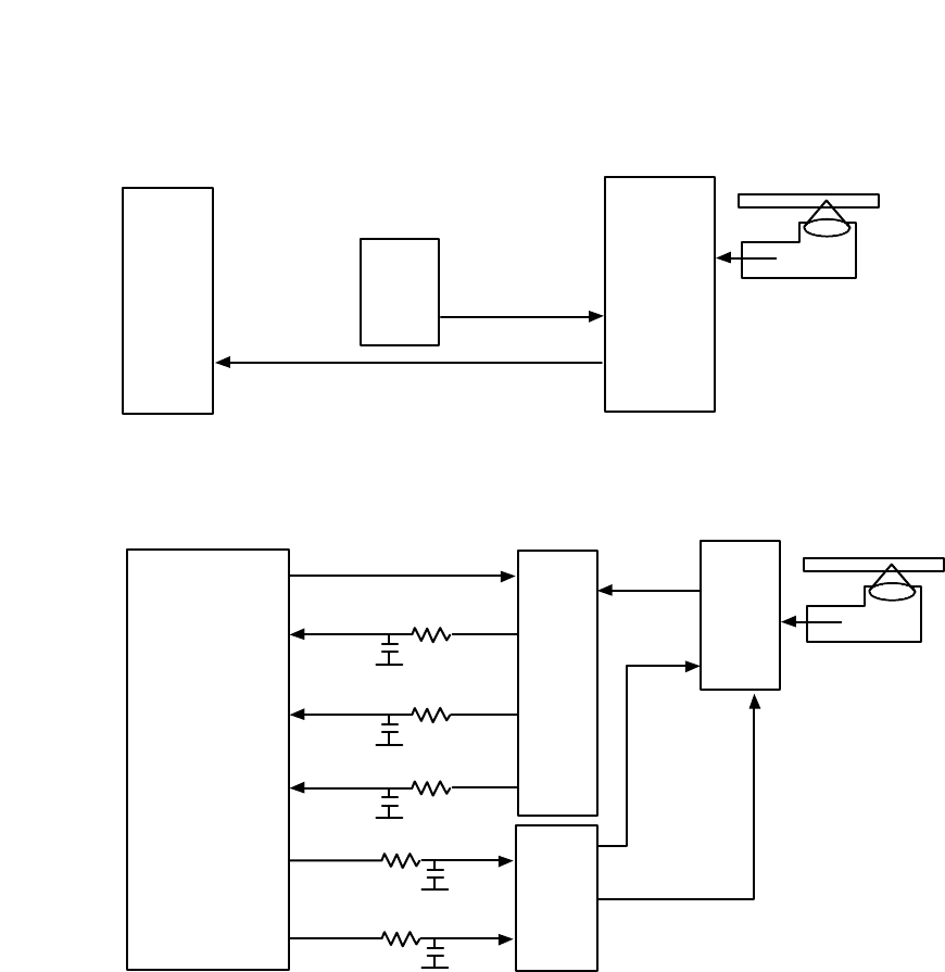
78
AFE
IC101
Driver
IC601
Slider/
Spindle
Spindle FFC
Slider FPC
Slider:#6,8-10
Pin#
87-90
MPU & DSP
IC301
AFE
IC101
Driver
IC601
Pickup
All Disc
FFC
Setting
FE:R102,C405
Focus:#34-35
Tracking:#30-31
Slider FPC
Slider:#6,8-10
TE:R101,C101
PE:R103,C406
R329,C335 FOD
TRD
R330, C336
#40
#1
#3
#2
#43
#39
(21) RTZ TimeOut Fail
(22) Focus Servo/Tracking Servo Fail

79
No. Error Code Contents of fail Fail Analysis Block Diagram
SSB Byte8,9
1 28xx LP Adjust NG. 1) Check Pickup FFC Connection. No.01
2) Check solder of IC101circumference.
(pin#6, 10, 12, L150, L151)
3) Check solder of IC102.
4) Exchange Pickup(LDD, Front Monitor).
5) Exchange IC101(AFE).
6) Exchange IC301(MPU & DSP).
2 48xx High Frequency Adjust NG. 1) Check Pickup FFC Connection. No.02
2) Exchange Pickup (LDD part).
3) Exchange IC301(DSP).
3 5Exx NRZi Skew Adjust NG. 1) Check Pickup FFC Connection No.02
2) Exchange Pickup (LDD part).
3) Exchange IC301(MPU & DSP).
4 4C0x to 4C4x Data Slice Adjust NG. 1) Check solder of IC101circumference. No.03
(pin# 79, L150, L151)
2) Exchange IC101(AFE).
3) Exchange IC301(MPU & DSP).
5 4C5x to 4C7x EQ Boost Adjust NG. 1) Check solder of IC101circumference.
(pin# 79, L150, L151)
2) Exchange IC101(AFE).
3) Exchange IC301(MPU & DSP).
6 4C80 RAW Slice Level Adjust NG. 1) Check solder of IC101circumference.
(pin# 79, L150, L151)
2) Exchange IC101(AFE).
3) Exchange IC301(MPU & DSP).
7 4CAx EQ Auto Frequency Adjust NG. 1) Check solder of IC101circumference.
(pin# 79, L150, L151)
2) Exchange IC101(AFE).
3) Exchange IC301(MPU & DSP).
Detail Error Code & Fail Analysis
1. Laser Power Initial Adjust
(Exchange
low/high byte)
Byte8: xxh
Byte9: 28h

80
No. Error Code Contents of fail Fail Analysis Block Diagram
SSB Byte21,22
1 42xx Circuit Offset Adjust NG. 1) Check Pickup FFC Connection. No.04
2) Check solder of IC101circumference .
(pin#,1,2,3 pin#87-90,
FE_Servo: R102, C405
TE_Servo: R101, C101
PE_Servo: R103, C406)
3) Exchange IC101(AFE).
4) Exchange Pickup.
5) Exchange IC301(MPU & DSP).
2 452x Focus Amp Adjust NG. 1) Check DVD-Dual Disc. No.05
(DVD-DL Only) 2) Check Pickup FCC Connection.
3) Check solder of IC101circumference.
(pin#1,2,3 pin#87-90,
FE_Servo: R102, C405)
4) Check Slider FPC Connection.
5) Exchange IC101(AFE).
6) Exchange IC601(Driver).
7) Exchange IC301(MPU & DSP).
3 450x Focus Amp Adjust NG. 1) Check Pickup FFC Connection. No.06
451x Total Amp Adjust NG. 2) Check solder of IC101circumference.
454x (pin#1,2,3 pin#87-90,
FE_Servo: R102, C405
PE_Servo: R103, C406)
3) Exchange Pickup.
4) Exchange IC101(AFE).
5) Exchange IC301(MPU & DSP).
4 458x Tracking Amp Adjust NG. 1) Check Pickup FFC Connection. No.07
2) Exchange Pickup.
3) Check solder of IC101circumference.
(pin#1,2,3 pin#87-90,
TE_Servo: R101, C101)
4) Exchange IC101(AFE).
5) Exchange IC301(MPU & DSP).
5 47xx Servo Loop Gain Adjust NG. 47XA: Disc Unmatch(Exchange Disc). No.08
1) Check Pickup FFC Connection.
2) Exchange Pickup (Signal Noisy).
3) Check solder of IC101circumference.
(pin#1,2,3 pin#87-90,
FE_Servo: R102, C405
TE_Servo: R101, C101)
4) Exchange IC101(AFE).
5) Exchange IC301(MPU & DSP).
6 49xx Unwritten Slice Level Adjust NG. 4906: RAM Disc NG (Exchange Disc). N0.09
(RAM Only) 1) Check solder of IC101circumference.
(pin#1,2,3 pin#87-90)
2) Exchange IC101(AFE).
3) Exchange IC301(MPU & DSP).
2. Adjusting Error during Disc Load Sequence (Lead in Error)

81
No. Error Code Contents of fail Fail Analysis Block Diagram
SSB Byte21,22
7 4Axx Focus Offset Adjust NG. 4A08: Disc Unmatch(Exchange Disc). No.10
(DVD-ROM,CD-R/RW) 1) Check Pickup FFC Connection.
2) Exchange Pickup.
3) Exchange IC301(MPU & DSP).
8 4A5x Focus Offset Adjust NG. 1) RAM Disc NG (Exchange RAM Disc) No.11
4A6x (RAM Only for PID) 2) Exchange Pickup
3) Exchange IC101(AFE)
4) Exchange IC301(MPU & DSP)
9 4A8x Focus Offset Adjust NG. 4A88: RAM Disc NG (Exchange RAM Disc). No.12
(RAM Only for Data) 1) Exchange Pickup.
2) Exchange IC101(AFE).
3) Exchange IC301(MPU & DSP)
10 4B0x Tilt Adjust NG(RAM Only). 1) Check Pickup FFC Connection. No.13
2) Exchange Pickup.
3) Check solder of IC101circumference.
(pin#6,7 R106, C106, R107, C107)
4) Exchange IC101(AFE).
5) Exchange IC301(MPU & DSP).
11 4B8x Tilt Adjust NG(DVD-/+ R/RW). 1) Check Pickup FFC Connection. No.14
2) Exchange Pickup.
3) Check solder of IC601 circumference.
4) Exchange IC601.
5) Check solder of IC301 circumference.
6) Exchange IC301
7) Exchange Slider Motor.
12 4CCx Data Slice Adjust NG. 1) Exchange Pickup. No.12
(RAM Only) 2) Exchange IC101(AFE).
3) Exchange IC301(MPU & DSP).
13 4Dxx Focus Deviation Adjust NG. 1) Check Pickup FFC Connection. No.15
2) Exchange Pickup.
3) Check solder of IC301circumference.
4) Exchange IC301(MPU & DSP).
14 182x Home Position Adjust NG. 1) Check FFC Connection. No.21
01xx (DVD-SL Only) 2) Check Slider FPC Connection.
3) Exchange Slider Motor.
4) Check solder of IC101circumference.
5) Exchange IC101(AFE).
15 52xx Focus Offset Adjust NG. 1) Check Pickup FFC Connection. No.16
(DVD-R/RW, +R/RW) 2) Exchange Pickup.
3) Check solder of IC101circumference.
(pin#1,2,3 pin#87-90,
TE_Servo: R101, C101)
4) Exchange IC101(AFE).

82
No. Error Code Contents of fail Fail Analysis Block Diagram
SSB Byte21,22
16 54xx DPP Amp Adjust NG. 1) Check Pickup FFC Connection. No.07
(CD Disc Only) 2) Exchange Pickup.
3) Check solder of IC101circumference.
(pin#1,2,3 pin#87-90,
TE_Servo: R101, C101)
4) Exchange IC101(AFE).
5) Exchange IC301(MPU & DSP).
17 55xx Lens Shift/ Tilt Adjust NG. 1) Check Pickup FFC Connection. No.14
(CD Disc Only) 2) Exchange Pickup.
3) Check solder of IC601 circumference.
4) Exchange IC601.
5) Check solder of IC301 circumference.
6) Exchange IC301
7) Excahange Slider Motor
18 56xx Focus Level Adjust NG. 1) Check Pickup FFC Connection. No.06
2) Exchange Pickup.
3) Check solder of IC101circumference.
(pin#1,2,3 pin#87-90,
PE_Servo: R103, C406)
4) Exchange IC101(AFE).
5) Exchange IC301(MPU & DSP).
19 57xx HFPE Amp/Gain Adjust NG. 1) Check Pickup FFC Connection. No.13
2) Exchange Pickup.
3) Check solder of IC101circumference.
(pin#6,7 R106, C106, R107, C107)
4) Exchange IC101(AFE).
5) Exchange IC301(MPU & DSP).
20 58xx Lens Sensitivity Adjust NG. 1) Check Pickup FFC Connection. No.17
2) Exchange Pickup.
3) Check solder of IC301circumference.
4) Exchange IC301(MPU & DSP).
21 59xx Spindle Offset Adjust NG. 1) Check Spindle FFC Connection. No.18
2) Check solder of IC601circumference.
(pin#12-14)
3) Exchange IC601(Driver).
4) Exchange Spindle Motor.
5) Check solder of IC301circumference.
6) Exchange IC301(MPU & DSP).

83
No. Error Code Contents of fail Fail Analysis Block Diagram
SSB Byte21,22
22 5Axx ADIP read timing Adjust NG. 5A01: Check DVD+R Disc (Exchange Disc) . No.19
1) Check Pickup FFC Connection.
2) Exchange Pickup.
3) Exchange IC101(AFE).
4) Exchange IC301(MPU & DSP).
5) Exchange IC601(Driver)
23 5Cxx Signal Amp Error. 1) Check Pickup FFC Connection. No.06
2) Exchange Pickup.
3) Check solder of IC101circumference.
(pin#1,2,3 pin#87-90,
PE_Servo: R103, C406)
4) Exchange IC101(AFE).
5) Exchange IC301(MPU & DSP).
24 5Dxx Focus Offset Adjust NG. 1) Check Pickup FFC Connection. No.20
(DVD-R/RW,+R/RW in Data) 2) Exchange Pickup.
3) Check solder of IC101circumference.
4) Exchange IC101.
5) Check solder of IC701circumference.
6) Exchange IC301(MPU & DSP).
7) Exchange Slider Motor.

84
No. Error Code Contents of fail Fail Analysis Block Diagram
SSB Byte21,22
1 2503,2504 RTZ Timeout(Sled Timeout). 1) Check Slider FPC Connection. No.21
2) Check solder of IC601 circumference .
(pin#2-3, 6, 8-10)
3) Exchange IC601.
4) Exchange Slider Motor.
2 2020,2021 Focus Fail. 1) Check Pickup FFC Connection. No.22
2) Exchange Pickup.
3) Check solder of IC601circumference.
4) Exchange IC601(Driver)
5) Check solder of IC101circumference.
(pin#1,2,3pin#87-90,
FE_Servo: R102, C405)
6) Exchange IC101(AFE).
3 2101,2102 Tracking Fail. 1) Check Pickup FFC Connection. No.22
2) Exchange Pickup.
3) Check solder of IC601circumference.
4) Exchange IC601(Driver).
5) Check solder of IC101circumference.
(pin#1,2,3 pin#87-90,
TE_Servo: R101, C101).
6) Exchange IC101(AFE).
4 2000~2010 Spindle Fail. 1) Check Spindle FFC Connection. No.18
2) Check solder of IC601circumference.
(pin#12-14)
3) Exchange IC601(Driver).
4) Exchange Spindle Motor.
5) Check solder of IC301circumference.
6) Exchange IC301(MPU & DSP).
3. Loading Sequence Error (Lead in Error)
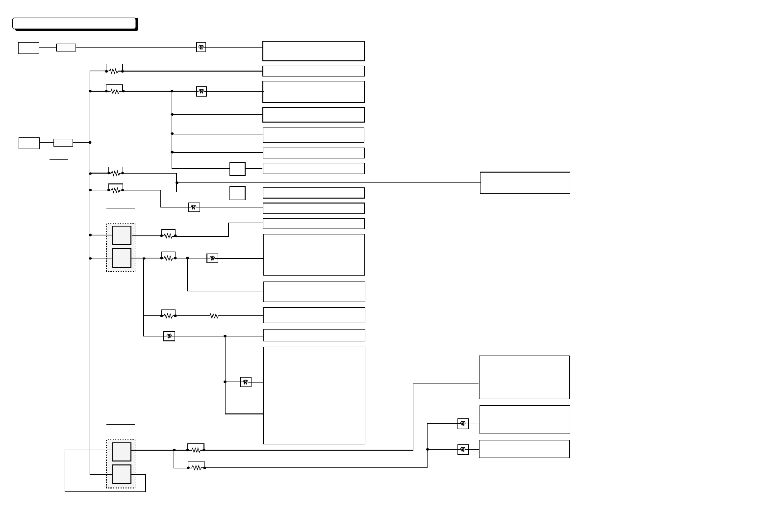
IC701
1.5V
REG
IC701
2.8V
REG
12V
DRV IC601 R2S30202FP
VM1 #22 Motor power supply 1(Spindle)
VM2 #05 Motor power supply 2(Slide)
IC301 DSP (R8J32007)
#028 VCC Core Power]
#041 VDD [Core Power]
#072 VDD [Core Power]
#130 VDD [Core Power]
#146 VDD [Core Power]
CN101 P/U (LDD) Vso5V #29
IC101 AFE(R2S35002)
VCC1 #08 Power (5.0V)
VCC2 #78 Power (5.0V)
IC102 LM258-D VCC #08
(ON SEMIconductor) OP-amp
Audio Output
Q901 Tr(UMC5N)/Q902 Tr(UMG4N)
CN101 P/U
OEIC(Vcc) #44 & FM(Vcc) #11
CN101 P/U Vsa5(Vcc) #15
Light Scribe Encoder Module Vcc 5V
Front PWB Led Control Vcc 5V
IC601 DRV 5VCC(#32)/VM3(#26)
CN101 P/U LDD Vsl2.8(Vcc) #16
IC101 AFE (R2S35002)
VDD1 #69 Power
VDD2 #91 Power
VDD3 #11 Power
VDD4 #59 Power
VDD5 #22 Power
SRVREF #82 Power
IC301 DSP (R8J32007)
VCCA #186 3.3V
VCCA #166 3.3V
IC301 DSP (R8J32007)
Audio VCCA #99 3.3V
IC302 Flash Memory Fujitsu/Mcronics
IC301 DSP (R8J32007)
#58 VCCIO [DSP I/O]
#75 VCCIO [DSP I/O]
#88 VCCIO [DSP I/O]
#108 VCCA [Analog]
#133 VCCIO [DSP I/O]
#139 VCCA [Analog]
#148 VCCIO [DSP I/O]
#185 VCCA [Analog]
#200 VCCIO [DSP I/O]
#53 VCCR [SDRAM]
#52 VCCIO [DSP I/O]
#32 VCCIO [DSP I/O]
#26 VCCRQ [SDRAM I/O]
#08 VCCRQ [SDRAM I/O]
#07 VCCIO [DSP I/O]
#02 VCCR [SDRAM]
12V
Vso
S705 OPEN
5V
2.5(2.8)
3.3A
3.3A
3.3A-2
3.3D
S713 OPEN
5VR
L151
L150
L602
L601
R354
0
UMC5N
Vin=5.00 V
V0=3.30 V
Pc= W
Vin=5.00 V
V0=2.80 V
Torex Regurator
IC703 XCM403AA03SR
miniSMDC150F/24
(Raychem)
L305
L710
1.5D
1.5A
IC703
2.8V
REG
IC703
3.3V
REG
SW701
Poly SW
5V in
miniSMDC150F/24
(Raychem)
SW702
Poly SW
S707 OPEN
S706 OPEN
S704 OPEN
5VP
S714 OPEN
S708 OPEN
S709 OPEN
L304
L301
Tr
Q631
UMC5N
Tr
Q651
Vin=5.00 V
V0=2.80 V
Pc= W
Vin=2.80 V
V0=1.50 V
Torex Regurator
IC701 XCM403AA02SR
S715 OPEN
IC301 DSP (R8J32007)
#189 VDDAA [Analog Power]
#193 VDDAA [Analog Power]
#197 VDDAA [Analog Power]
IC301 DSP (R8J32007)
#159 VDDAA [Analog Power]
85 86
JR6 Power Supply System Diagram * Ver1.0 It created based on the PLT circuit diagram.

87
No Circuit/IC Signal Signal/Level mesurement-point (IC-pin or Device)
1 Power supply Line-12V 12V CN801-41
2 Line-5V 5V CN801-44
3 (IC701) reg-1.5V 1.5V IC701-2
4 reg-2.8V 2.8V IC703-5
5 (IC703) reg-3.3V 3.3V IC703-2
6 Flash-ROM VDD : 3.3V 3.3V 37
7 (IC302) CS Active-Low 26
8 XRD read-CK 28
9 DSP VDD : 1.5V 1.5V 41, 28, 72, 130, 146, 159, 189, 193, 197
10 (IC301) VCC(D) : 3.3V 3.3V 7, 32, 52, 58, 75, 88, 133, 148, 200, 199, 2, 53, 185,
139, 108, 8, 26
11 VCC(A) : 3.3V 3.3V 186, 166, 99
12 Clock-34MHz 33.8688MHz 106, 107
13 MRSTB (3.3V)High 202
14 AFE VCC : 5.0V 5.0V 8, 78
15 (IC101) VDD : 3.3V 3.3V 22, 11, 91, 59, 69, 82
16 OP-amp VCC : 5.0V 5.0V 8
(IC102)
17 7ch-DRV 5VCC : 5V 5V 32
18 (IC601) VM3 : 5V 5V 26
19 VM1, 2 : 12V 12V 5, 22
20 REF : 1.65V 1.65V 42
21 Pick-up VCC(FM) : 5.0V 5.0V 11
22 VCC(OEIC) : 5.0V 5.0V 44
23 VC(OEIC) : 2.1V 2.1V 43
24 VREF : 2.5V 2.5V 9
25 VSL25 : 2.8V 2.8V 16
26 VSA5 : 5.0V 5.0V 15
27 VSO : 5.0V 5.0V 29
* When there are twe or more power supply pins of LSI, it checks by one ramdom pin first.
PCB Poor Analysis - Check list

88
1. Self-Diagnostic Function by LED Blink.
• Basic operation: At JR6, MPU is included in DSP, MPU accesses each peripheral (inside, exterior) device,
and discover a defect by the ability of a read/write of data to be performed correctly. Since MPU operates by
the program with a built-in Flash-ROM, when abnormalities are in MPU, Flash-ROM, and these Data-Bus &
control signals, this self-diagnostic function cannot be used. In such a case, the case where LED does not
light up at all at the time of a power supply injection is almost the case.
• MPU: In DSP Flash-ROM (16Mb) is connected to the exterior Bus of MPU. Even if the MPU-Bus terminal of
Flash-ROM short-circuits, it becomes impossible for MPU to read the right program data from Flash-ROM,
and stops for this reason, turning on LED at all. On the other hand, the own poor device of DSP, and the
open state of IC-pin, when a defect does not influencing Bas of MPU, it can detect correctly and becomes
blink of LED according to those defects.
• DSP: DSP has ATAPI-IF, LDD-serial-IF, AFE-serial-IF, and an AFE control signal as Digital-IF. As Analog-
IF, it has the slice circuit of RF signal from AFE, PLL, the objects ADC and DAC for SERVO, and ADC for
ADIP detection. Among these, own poor Digital of DSP, and AFE-serial-IF can detect by this self-diagnostic
function.
• AFE: Poor detection of AFE is restricted to detection of a limitation-item. Since the greater part of the
function is analog signal processing, AFE serves as a register in AFE, and a check, which accepts it, serial
IF in the logical digital examination from MPU. In addition, serial-IF for AFE control is performed via DSP.
This is writing in the Write command and setting data, and is automatically transmitted to the predetermined
register of DSP. Conversely, when it leads the register information on AFE, the read command can be
written in the predetermined register of DSP, and the value of an AFE register can be read by reading the
read register of DSP after that. Therefore, serial [between the poor register of AFE, and AFE and DSP],
when there is LED blink with poor AFE — the defect of IF or the defect of the register for AFE of DSP is
considered.
•Refer to the contrast table of the number of times of blink of LED, and a poor part.
•The self-diagnostic function by this LED blink is carried out in the state of a set without a PCB independent
or loading Disc.
HW Self- Diagnostic function

89
2. LED does not blink at all at the time of a power supply injection. Eject-SW does not react.
(1) Is it normal to the exterior Bus (Data-Bus, Address-Bus, control signal system) of MPU?
Viewing — check: -- a short circuit, opening, etc.
• The device connected to the exterior Bus of MPU in DSP, and its signal list
=> It repairs, when abnormalities are discovered.
(2) Does the power supply circuit operate normally?
External input 12V, external input 5V, regulator 3.3V, regulator 2.8V, and regulator 1.5V
=>When the abnormalities are discovered, an external power supply, a power supply cable, and Regulator
IC are exchanged.
=> Since a problem is in a load side when not improving, even if it exchanges the above, and attached sheet
JR6 power-supply system figure is made reference, and poor portions, such as a short circuit of a power
supply part, are found out and fixed.
(3) Is the clock of MPU in DSP oscillated correctly?
Checked the ceramic oscillation element’s X301 both-ends and DSP(106)(107) 33.87MHz oscillating.
=> When 3.3V power supply is correctly supplied to DSP and the clock is not oscillating correctly, it is the
defect of MPU, or an oscillation element defect, and part exchange is performed in order of DSP and
X301.
(4) The defect of Flash-ROM
Although the clock of DSP is oscillating correctly and the power supply circuit is also outputting normal
voltage, when LED does not blink at all at the time of a power supply injection and Eject-SW does not react,
either, poor Flash-ROM is the most doubtful.
=> Flash-ROM (IC302) are exchanged.
Note: Before Flash-ROM exchange, the CS signals of the external device of MPU in DSP connection, an
Address signal, and a Data signal are observed on a waveform level, and since the but most amount of work
and the special knowledge which can raise the discovery accuracy of a poor part are necessities,
recommendation is impossible.
(5) Even if it performs the above-mentioned repair, when not improving, the disconnection and the short circuit
which cannot be discovered, can be considered in viewing of PCB. Moreover, partial breakage (although a
clock is oscillated, somewhere in insides do not operate.) of DSP can be considered.
=> When not improving above, the possibility that a PCB pattern is faulty is high, and judges repair to be
difficult.
Peripheral device Flash -ROM
[Bus/Signal] (IC302)
Address A1~A20
Data D0~D15
CS* CS0B
WCK WR
RCK RD

90
3. Motor, Abnormalities in Actuator System
The drive circuit of a motor & actuator consists of the three ICs IC601(R2S30202FP). The work of each IC is
as follows.
(1) IC601(R2S30202FP) : 7ch driver
Spindle motor driver: 180° audio drive Type, an analog input, a PWM drive, a Vm=12V.
Stepping motor driver X2: analog input, a PWM drive (differential), a Vm=12V
Loading motor driver: Input/Output PWM drive, Vm=5V.
Focus actuator driver: analog input / output (differential), a Vm=5V
Tracking actuator driver: analog input / output (differential), Vm=5V
Tilt actuator driver : analog input/output (differential), Vm=5V.
A motor & actuator and its correspondence pin
A control mode setup by the control terminal
Signal/CH SPDL-MT STEP-MT Load-MT Focus-ACT Track-ACT Tilt-ACT
Input (1)SPIN (2)SL1IN (41)LOIN (40)FOIN (39)TOIN (38)TLIN
(3)SL2IN
Reference (42)REF 1.65V
Output (12)U (6)SL2+ (27)LO+ (34)FO+ (31)TO+ (36)TL+
(13)V (8)SL2- (28)LO- (35)FO- (30)TO- (37)TL-
(14)W (9)SL1+
(10)SL1-
EN1(20) EN2(21) SPDL SLED Load Focus/Track/Tilt
Low Low off off off off
Low High off on on off
High Low on on off on
High High on on off on
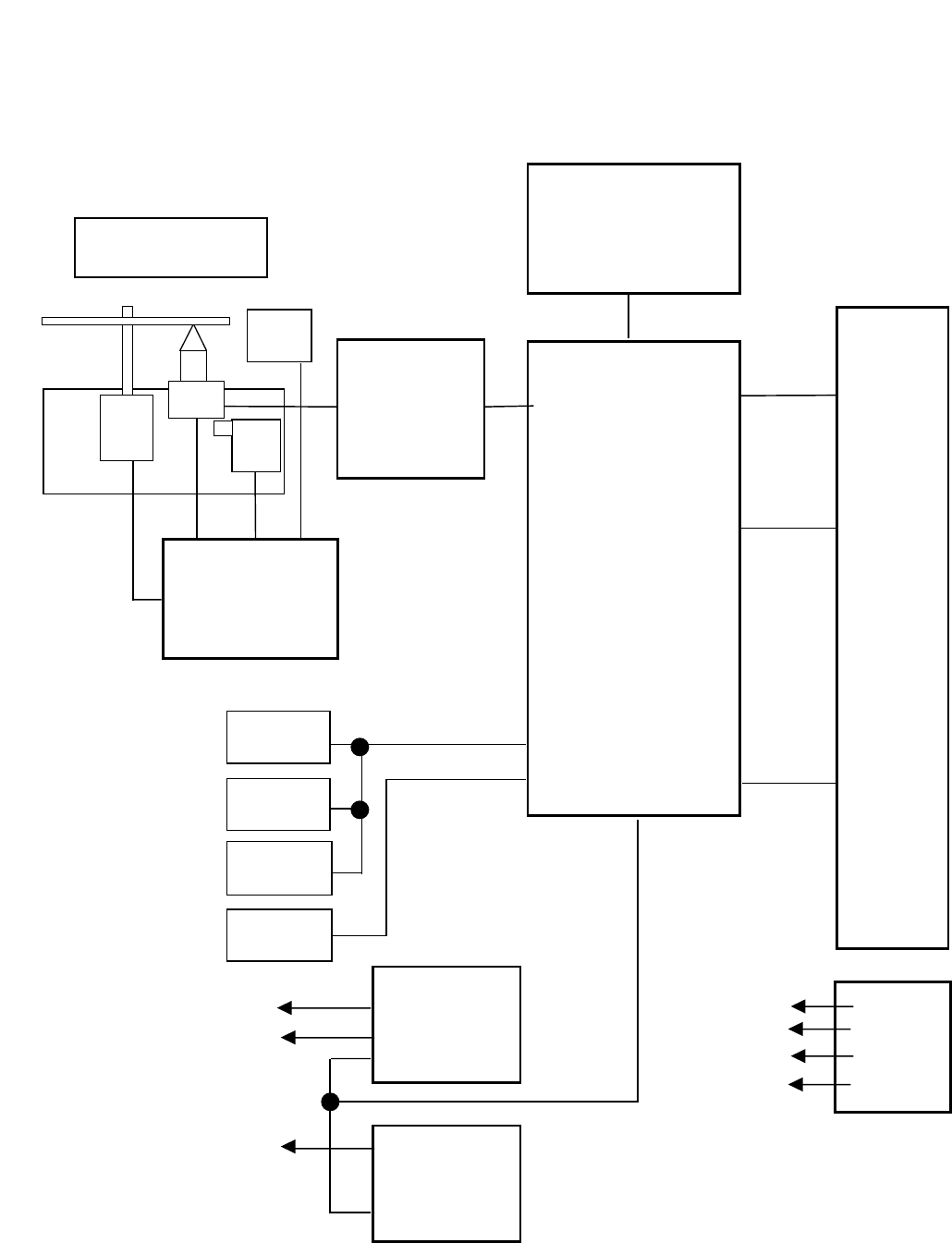
91
12V
GND
5V
Device
configuration
jumper
MASTER
SLAVE
CSEL
Host IDE
Analog
audio
LED
3.3V
2.8V
1.5V
Flash-ROM
(2MByte)
MBM29LV160BE
or Equivalent
(FUJITSU)
Disc
Loading
motor
Slide
motor
Disc
motor
Unit
mechanism
Tray Detect
SW
Eject
SW
Limit
SW
Analog Front End
R2S35002
100pin-TQTF
(RENESAS)
3.3V/2.8V Reg.IC
XCM403AA03SR
RST
(TOREX)
2.8V/1.5V Reg.IC
XCM403AA02SR
RST
(TOREX)
OPU:HOP-7632TS
(HITACHI ME)
Interface
connector
DVD/CD DSP
(DVD/CD/Servo/ATAPI)
R8J32007FP
256pin LQFP
(RENESAS)
DVD-codec
CD-codec
LPP/ADIP decorder
Servo DSP
ATAPI-IF
Microprocessor
7ch-Driver
R2S30202FP
SPDL/SLED/Fo/Tr/Ti/LD
(RENESAS)
PU
BLOCK DIAGRAM
