Lg C320 Users Manual C320_SVC ENG_101007
LG-C320 to the manual e3475751-5423-4144-b3a9-4de7607efb28
2015-01-26
: Lg Lg-Lg-C320-Users-Manual-229466 lg-lg-c320-users-manual-229466 lg pdf
Open the PDF directly: View PDF ![]() .
.
Page Count: 174 [warning: Documents this large are best viewed by clicking the View PDF Link!]
Service Manual Model : LG-C320
Internal Use Only
Service Manual
LG-C320
Date: October, 2010 / Issue 1.0

- 3 -
Copyright © 2010 LG Electronics. Inc. All right reserved.
Only for training and service purposes
LGE Internal Use Only
Table Of Contents
1. INTRODUCTION ..................................................................5
1.1 Purpose ............................................................................................... 5
1.2 Regulatory Information ............................................................... 5
1.3 Abbreviations ................................................................................... 7
2. PERFORMANCE ...................................................................9
2.1 Product Name .................................................................................. 9
2.2 Supporting Standard .................................................................... 9
2.3 Main Parts : GSM Solution ........................................................... 9
2.4 HW Features ....................................................................................10
2.5 SW Features ....................................................................................12
2.6 HW SPEC. .........................................................................................14
2.7 C320 Figures ...................................................................................15
3. TECHNICAL BRIEF .............................................................16
3.1 General Description .....................................................................16
3.2 Power management ....................................................................28
3.3 SUB SYSTEM ....................................................................................32
3.4 General Description (RF Part) ..................................................40
3.5 GSM MODE ......................................................................................41
3.6 OFF-CHIP RF COMPONENTS ....................................................44
3.7 OFF-CHIP COMPONENTS ..........................................................46
4. TROUBLE SHOOTING .......................................................50
4.1 Power ON Troubleshooting ......................................................50
4.2 Charger Troubleshooting ..........................................................52
4.3 USB Troubleshooting ..................................................................54
4.4 USIM Detect Troubleshooting .................................................56
4.5 Camera Troubleshooting ...........................................................58
4.6 Main side view LED Troubleshooting ...................................60
4.7 Slide Key side view LED Troubleshooting ...........................61
4.8 LCD Troubleshooting ..................................................................63
4.9 Vibrator Troubleshooting ..........................................................65
4.10 Receiver Path ...............................................................................67
4.11 Headset path ...............................................................................70
4.12 Speaker/Speaker Phone path ...............................................73
4.13 Main microphone ......................................................................78
4.14 Headset microphone ................................................................80
4.15 RF Component ............................................................................82
4.16 RF Path ............................................................................................83
4.17 Trouble Shooting of GSM Part ..............................................84
4.18 Checking Bluetooth Block ......................................................91
4.19 Checking FM Radio Block .......................................................96
5. DOWNLOAD ......................................................................99
6. BLOCK DIAGRAM ........................................................... 112
7. CIRCUIT DIAGRAM ........................................................ 123
8. BGA Pin Map .................................................................. 137
9. PCB LAYOUT ................................................................... 143
10. RF CALIBRATION ......................................................... 149
10.1 Usage of Tachyon for RF Calibration and Test ............. 149
11. TEST ALONE ................................................................. 152
11.1 Phone Test Mode.....................................................................152
12. EXPLODED VIEW & REPLACEMENT PART LIST ......... 157
11.1 EXPLODED VIEW ...................................................................... 157
11.2 Replacement Parts.................................................................. 159
11.3 Accessory ................................................................................... 175

- 4 -
LGE Internal Use Only Copyright © 2010 LG Electronics. Inc. All right reserved.
Only for training and service purposes

- 5 -
Copyright © 2010 LG Electronics. Inc. All right reserved.
Only for training and service purposes
LGE Internal Use Only
1. INTRODUCTION
1. INTRODUCTION
Introduction
1.1 Purpose
This manual provides the information necessary to repair, calibration, description and download the features
of this model.
1.2 Regulatory Information
A. Security
Toll fraud, the unauthorized use of telecommunications system by an unauthorized part (for example,
persons other than your company’s employees, agents, subcontractors, or person working on your
company’s behalf) can result in substantial additional charges for your telecommunications services. System
users are responsible for the security of own system.
There are may be risks of toll fraud associated with your telecommunications system. System users are
responsible for programming and configuring the equipment to prevent unauthorized use. The
manufacturer does not warrant that this product is immune from the above case but will prevent
unauthorized use of common carrier telecommunication service of facilities accessed through or connected
to it. The manufacturer will not be responsible for any charges that result from such unauthorized use.
B. Incidence of Harm
If a telephone company determines that the equipment provided to customer is faulty and possibly causing
harm or interruption in service to the telephone network, it should disconnect telephone service until repair
can be done. A telephone company may temporarily disconnect service as long as repair is not done.
C. Changes in Service
A local telephone company may make changes in its communications facilities or procedure. If these
changes could reasonably be expected to affect the use of the phones or compatibility with the net work, the
telephone company is required to give advanced written notice to the user, allowing the user to take
appropriate steps to maintain telephone service.
D. Maintenance Limitations
Maintenance limitations on the phones must be performed only by the manufacturer or its authorized agent.
The user may not make any changes and/or repairs expect as specifically noted in this manual. Therefore,
note that unauthorized alternations or repair may affect the regulatory status of the system and may void
any remaining warranty.
- 6 -
LGE Internal Use Only Copyright © 2010 LG Electronics. Inc. All right reserved.
Only for training and service purposes
1. INTRODUCTION
G
E. Notice of Radiated Emissions
This model complies with rules regarding radiation and radio frequency emission as defined by local
regulatory agencies. In accordance with these agencies, you may be required to provide information such as
the following to the end user.
F. Pictures
The pictures in this manual are for illustrative purposes only; your actual hardware may look slightly different.
G. Interference and Attenuation
A phone may interfere with sensitive laboratory equipment, medical equipment, etc. Interference from
unsuppressed engines or electric motors may cause problems.
H. Electrostatic Sensitive Devices
ATTENTION
Boards, which contain Electrostatic Sensitive Device (ESD), are indicated by the sign. Following
information is ESD handling:
• Service personnel should ground themselves by using a wrist strap when exchange system boards.
• When repairs are made to a system board, they should spread the floor with anti-static mat which is also
grounded.
• Use a suitable, grounded soldering iron.
• Keep sensitive parts in these protective packages until these are used.
• When returning system boards or parts like EEPROM to the factory, use the protective package as described.
- 7 -
Copyright © 2010 LG Electronics. Inc. All right reserved.
Only for training and service purposes
LGE Internal Use Only
1. INTRODUCTION
ʹΠΡΪΣΚΘΙΥ͑ι ͣͨ͑͡͡ͽ͑ͶΝΖΔΥΣΠΟΚΔΤ͑͟ͺΟΔ͑͑͟ͲΝΝ͑ΣΚΘΙΥ͑ΣΖΤΖΣΧΖΕ͑͟
ΟΝΪ͑ΗΠΣ͑ΥΣΒΚΟΚΟΘ͑ΒΟΕ͑ΤΖΣΧΚΔΖ͑ΡΦΣΡΠΤΖΤ
ͽͶ͑ͺΟΥΖΣΟΒΝ͑ΆΤΖ͑ΟΝΪ 6/140
1.3 Abbreviations
For the purposes of this manual, following abbreviations apply:
Offset Phase Locked LoopOPLL
Light Emitting DiodeLED
Low Drop OutputLDO
Liquid Crystal DisplayLCD
Intermediate FrequencyIF
International Portable User IdentityIPUI
Global System for Mobile CommunicationsGSM
General Purpose Interface BusGPIB
Gaussian Minimum Shift KeyingGMSK
Flexible Printed Circuit BoardFPCB
Electrostatic DischargeESD
Electrical Erasable Programmable Read-Only MemoryEEPROM
Digital Signal ProcessingDSP
dB relative to 1 milli wattdBm
Digital Communication SystemDCS
Digital to Analog ConverterDAC
Constant Current – Constant VoltageCC-CV
Bit Error RatioBER
BasebandBB
Automatic Power ControlAPC
1. INTRODUCTION
- 8 -
LGE Internal Use Only Copyright © 2010 LG Electronics. Inc. All right reserved.
Only for training and service purposes
1. INTRODUCTION
ʹΠΡΪΣΚΘΙΥ͑ι ͣͨ͑͡͡ͽ͑ͶΝΖΔΥΣΠΟΚΔΤ͑͟ͺΟΔ͑͑͟ͲΝΝ͑ΣΚΘΙΥ͑ΣΖΤΖΣΧΖΕ͑͟
ΟΝΪ͑ΗΠΣ͑ΥΣΒΚΟΚΟΘ͑ΒΟΕ͑ΤΖΣΧΚΔΖ͑ΡΦΣΡΠΤΖΤ
ͽͶ͑ͺΟΥΖΣΟΒΝ͑ΆΤΖ͑ΟΝΪ 7/140
Wireless Application Protocol
WAP
Voltage Control Temperature Compensated Crystal OscillatorVCTCXO
Voltage Controlled OscillatorVCO
Universal Asynchronous Receiver/TransmitterUART
Time Division Multiple AccessTDMA
Time Division DuplexTDD
Travel AdapterTA
Side Tone Masking RatingSTMR
Pseudo SRAMPSRAM
Static Random Access MemorySRAM
Sending Loudness RatingSLR
Subscriber Identity ModuleSIM
Surface Acoustic WaveSAW
Real Time ClockRTC
Root Mean SquareRMS
Receiving Loudness RatingRLR
Radio FrequencyRF
Public Switched Telephone NetworkPSTN
Phase Locked LoopPLL
Programmable Gain AmplifierPGA
Printed Circuit BoardPCB
Power Amplifier ModulePAM
1. INTRODUCTION
- 9 -
Copyright © 2010 LG Electronics. Inc. All right reserved.
Only for training and service purposes
LGE Internal Use Only
2. PERFORMANCE
2. PERFORMANCE
3
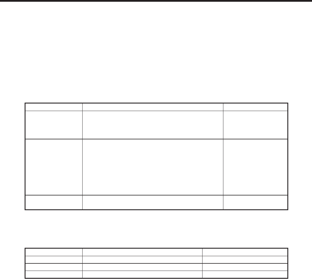
2.1 Product Name
C320 : EGSM/GSM850/DCS/PCS
(GPRS Class 12 / EDGE Class 12)
2.2 Supporting Standard
Item Feature Comment
Supporting Standard EGSM/GSM850/DCS1800/PCS1900
with seamless handover
Phase 2+(include AMR)
SIM Toolkit : Class 1, 2, 3, C-E
Frequency Range EGSM TX : 880 – 915 MHz
EGSM RX : 925 – 960 MHz
GSM850 TX : 824 – 849 MHz
GSM850 RX : 869 – 894 MHz
DCS1800 TX : 1710 – 1785 MHz
DCS1800 RX : 1805 – 1880 MHz
PCS1900 TX : 1850 – 1910 MHz
PCS1900 RX : 1930 – 1990 MHz
Application Standard WAP 2.0, JAVA 2.0
2.3 Main Parts : GSM Solution
Item Part Name Comment
Digital Baseband ESC6270 : Qualcomm
Analog Baseband ESC6270 : Qualcomm
RF Chip ESC6270 : Qualcomm
Phase 2+(include AMR)
SIM Toolkit : Class 1, 2, 3, C-E
- 10 -
LGE Internal Use Only Copyright © 2010 LG Electronics. Inc. All right reserved.
Only for training and service purposes
2. PERFORMANCE
4
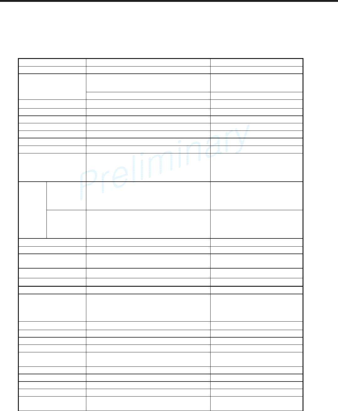
2.4 HW Features
Item Feature Comment
Form Factor Slide type
1) Capacity
Standard : Li-Ion, 900 mAh
Battery
2) Packing Type : Soft Pack
Size Standard : 91 x 63 x 15.9 mm
Weight 115.6g With Battery
Volume TBD
PCB Stag type, 10 Layers , 0.8t
Stand by time Up to 300 hrs @ Paging Period 5
Charging time Up to 3 hrs @
Talk time 2G Up to 3.4hr @ Tx=Max(2G)
RX sensitivity EGSM : -105 dBm
GSM850 : -105 dBm
DCS 1800 : -105 dBm
PCS 1900 : -105 dBm
GSM/
GPRS
EGSM : 33dBm
GSM850 : 33 dBm
DCS 1800 : 30 dBm
PCS 1900 : 30 dBm
Class4 (EGSM)
Class4 (GSM850)
Class1 (PCS)
Class1 (DCS)
TX
output
power
EDGE GSM 900 : 27 dBm
GSM 850 : 27 dBm
DCS 1800 : 26 dBm
PCS 1900 : 26 dBm
E2 (GSM900)
E2 (GSM850)
E2 (PCS)
E2 (DCS)
GPRS compatibility GPRS Class 12
EDGE compatibility EDGE Class 12
SIM card type Plug-In SIM
3V /1.8V
Display 2.4” TFT QVGA landscape
Built-in Camera 2M FF SOC Camera
Status Indicator Yes
Keypad
ANT Main : Internal Fixed Type
System connector 5 Pin
Ear Phone Jack 3.5Phi, 4 Pole, Stereo
PC synchronization Yes
Memory NAND Flash : 2Gbit
SDRAM : 1Gbit
Speech coding FR, EFR, HR,AMR
Data & Fax Built in Data & Fax support
Vibrator Built in Vibrator
BlueTooth V2.1 + EDR
MIDI(for Buzzer
Function)
SW Decoded 64Poly
- 11 -
Copyright © 2010 LG Electronics. Inc. All right reserved.
Only for training and service purposes
LGE Internal Use Only
2. PERFORMANCE
5
Music Player MP3/AAC/AAC+/WMA
Video Player PEG4, H.263,H.264 30fps@QVGA
WMV 15fps@QCIF
Camcorder MPEG4, 15fps@QVGA
Voice Recording Yes
Speaker Phone mode
Support
Yes
Travel Adapter Yes
CDROM No
Stereo Headset Yes
Data Cable Yes
T-Flash
(External Memory)
Yes
- 12 -
LGE Internal Use Only Copyright © 2010 LG Electronics. Inc. All right reserved.
Only for training and service purposes
2. PERFORMANCE
6
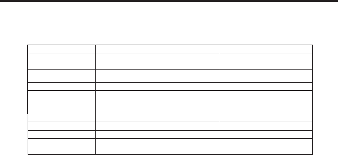
2.5 SW Features
Item Feature Comment
RSSI 0 ~ 7 Levels
Battery Charging 0 ~ 3 Levels
Key Volume 0 ~ 7 Level
Audio Volume 1 ~ 20 Level
Time / Date Display Yes
Multi-Language Yes English / Chinese Trad. / Chinese Simp.
/ Thai / Korean / Malay / Indonesian /
Vietnamese
Quick Access Mode Dialing / Contact / Menu /
Message / Camera
PC Sync Yes PC suite 4
Speed Dial Yes Voice mail center -> 1 key
Profile Yes not same with feature phone setting
CLIP / CLIR Yes
Phone Book Name + 5 Numbers + 1 Memo + 2
e-mail + 3 Group Select + Picture +
Ringtone + Anniversary day
1000 + SIM
Last Dial Number Yes Total Call DB Max 100
LDN (SIM) N/A
Last Received
Number
Yes Total Call DB Max 100
LDN (SIM) N/A
Last Missed Number Yes Total Call DB Max 100
LDN (SIM) N/A
Search by Number
/ Name
Name and Number
Group Yes 30
Fixed Dial Number Yes
Service Dial Number No
Own Number Yes Read only
(add/edit/delete are not supported)
Voice Memo Yes Support voice recorder
Call Reminder Yes
Network Selection Automatic
Mute Yes
Call Divert Yes
Call Barring Yes
Call Charge (AoC) Yes
Call Duration Yes
SMS (EMS) Yes (1000+SIM) EMS : Release4
(Except Text align)
SMS Over GPRS Yes
EMS Melody / Picture
Send / Receive / Save
Yes
(Receive only)
MMS MPEG4
Send / Receive / Save
Yes
Long Message MAX 1000 Characters SMS 7pages
- 13 -
Copyright © 2010 LG Electronics. Inc. All right reserved.
Only for training and service purposes
LGE Internal Use Only
2. PERFORMANCE
7
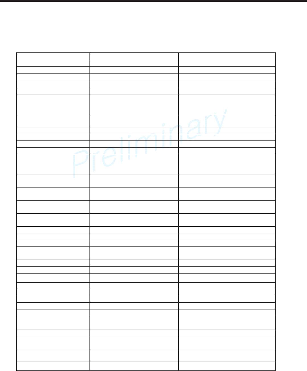
Cell Broadcast Yes
Download Over the WAP
Game Yes
Calendar Yes
Memo Yes 100
World Clock Yes
Unit Convert Yes
Stop Watch Yes
Wall Paper Yes
WAP Browser Over WAP 2.0 Obigo
Download Melody /
Wallpaper
Yes Over WAP
SIM Lock Yes Operator Dependent
SIM Toolkit Yes R99
MMS Yes Obigo +LG MMS Client
EONS No
CPHS Yes V4.2
ENS No
Camera Yes 2M FF
JAVA Yes CLDC V1.1 / MIDP V2.1
Download Over WAP
Voice Dial No
IrDa No
Bluetooth Yes BT 2.1+EDR
HFP/HSP/A2DP&AVRCP
/OPP/BPP/PBAP/SPP/
FM radio Yes
GPRS Yes Class 12
EDGE Yes Class 12
Hold / Retrieve Yes
Conference Call Yes Max. 6
DTMF Yes
Memo pad Yes
TTY No
AMR Yes
SyncML No
IM Yes JAVA midlet (neustar)
Email Yes
- 14 -
LGE Internal Use Only Copyright © 2010 LG Electronics. Inc. All right reserved.
Only for training and service purposes
2. PERFORMANCE
8
2.6 HW SPEC.
1) GSM transceiver specification
Item Specification
Phase Error Rms : 5°
Peak : 20 °
Frequency Error GSM : 0.1 ppm
DCS/PCS : 0.1 ppm
EMC(Radiated Spurious Emission
Disturbance) GSM/DCS : < -28dBm
Transmitter Output power and Burst
Timing
GSM : 5dBm – 33dBm ± 3dB
DCS/PCS : 0dBm – 30dBm ± 3dB
Burst Timing <3.69us
Spectrum due to modulation out to less
than 1800kHz offset
200kHz : -36dBm
600kHz : -51dBm/-56dBm
Spectrum due to modulation out to
larger than 1800kHz offset to the edge
of the transmit band
GSM :
1800-3000kHz :< -63dBc(-46dBm)
3000kHz-6000kHz : <-65dBc(-46dBm)
6000kHz < : < -71dBc(-46dBm)
DCS :
1800-3000kHz :< -65dBc(-51dBm)
6000kHz < : < -73dBc(-51dBm)
Spectrum due to switching transient 400kHz : -19dBm/-22dBm(5/0), -23dBm
600kHz : -21dBm/-24dBm(5/0), -26dBm
Reference Sensitivity – TCH/FS Class II(RBER) : -105dBm(2.439%)
Usable receiver input level range 0.012(-15 - -40dBm)
Intermodulation rejection – Speech
channels
± 800kHz, ± 1600kHz
: -98dBm/-96dBm (2.439%)
AM Suppression
TGSM : -31dBm
- DCS : -29dBm
-98dBm/-96dBm (2.439%)
Timing Advance ± 0.5T
- 15 -
Copyright © 2010 LG Electronics. Inc. All right reserved.
Only for training and service purposes
LGE Internal Use Only
2. PERFORMANCE
9
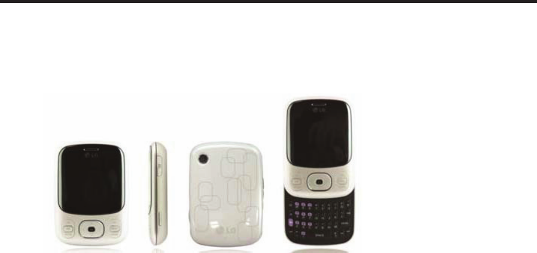
2.7 C320 Figures
- 16 -
LGE Internal Use Only Copyright © 2010 LG Electronics. Inc. All right reserved.
Only for training and service purposes
3. TECHNICAL BRIEF
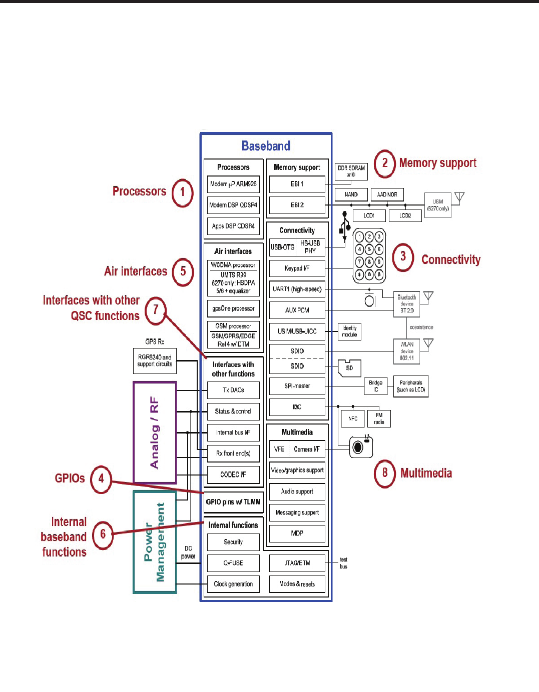
3. TECHNICAL BRIEF
2. Base Band Technical Description
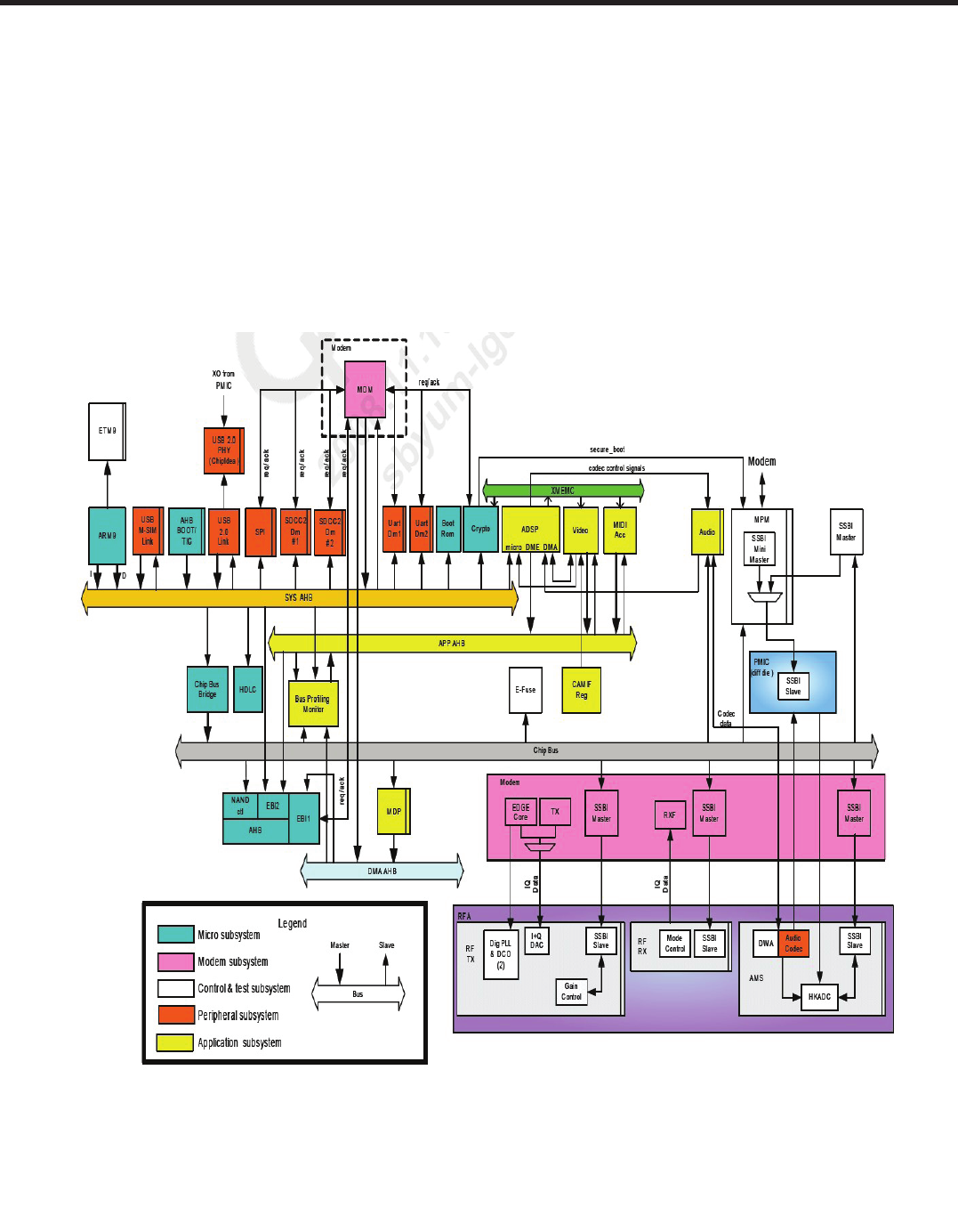
3.1 General Description
QSC6270 (3G disable)has all eight major functional blocks as like Figure 3.1
Figure 3.1 QSC6270(3G disable) Base band block
- 17 -
Copyright © 2010 LG Electronics. Inc. All right reserved.
Only for training and service purposes
LGE Internal Use Only
3. TECHNICAL BRIEF
3.1.1 Processor
The QSC6270(3Gdisable) device integrates multiple processors on-chip: one ARM microprocessor and two
DSP processors. Each processor is part of a functional subsystem:
The micro subsystem includes the ARM926EJ-S microprocessor.
The modem subsystem includes the QDSP4u8 digital signal processor (mDSP).
The application subsystem includes the QDSP4u8 application digital signal processor(aDSP).
Figure 3.1.1 Processors and bus architecture
- 18 -
LGE Internal Use Only Copyright © 2010 LG Electronics. Inc. All right reserved.
Only for training and service purposes
3. TECHNICAL BRIEF
3.1.2 Memory support (and LCD interface)
The QSC62x0 device has two external bus interface (EBI) ports: EBI1 and EBI2.
EBI1 supports high-speed synchronous dynamic devices. Its memory controller supports the new mobile
DDR SDRAM memories with its higher bandwidth and ability to run at high clock frequencies. This
interface supports the high-bandwidth, high-density, and low-latency requirements of the QSC’s
advanced on-chip capabilities such as the ARM9 processor, highperformance graphics, and video
applications.
EBI2 is the slower speed interface intended to support memory devices such as NAND flash and
asynchronous SRAM, peripheral devices such as LCDs, and the UBM receiver for multicast or
broadcast reception (QSC6270 only). In addition, EBI2 is required to support a synchronous-burst
AAD NOR flash to enable a NOR/DDR SDRAM memory configuration because the simultaneous mode
(NOR, SDRAM) is not supported on the EBI1 bus.
The ARM926EJ-S microprocessor is a cached processor and all its accesses to external memory use burst
techniques of four or eight 32-bit words when the memory region is declared to be
cacheable/bufferable. To take advantage of this QSC higher performance feature, data from
memories must satisfy the requirements for these burst accesses.
Figure 3.1.2.1 The memory control blocks of C320
QSC6270
NAND Flash
(1Gbit)
SDRAM
512Mbit)
NAND_DATA[ 0: 15]
NAND__CS__N
NAND_LB_N
NAND_UB_N
NAND_OE_N
NAND_WE_N
NAND_BSY_N
NAND_WP_N
_CE
ALE
CLE
_RE
_WE
RY_BY
_WP
IO[1: 16]
DDR_A[0:13]
DDR_M_CLK_N
DDR_CKE[0]_
DDR_CS[0]_N_
DDR_RAS_N
DDR_CAS_N
DDR_WE_N_ _
DDR_DQM[0:1]_
DDR_D[0:15]
CLK
CKE
_CS
_RAS
_CAS
_WED
DQM
ADDR
DQ
EBI1 EBI2
(3G disable)
USIM
(SIM PLUS)
SIM_CLK
_ _
SIM_DATA
MUSIM_DM
MUSIM_DP
SIM_RST_N
External
Memory
( MICRO SD)
MSD_D[0:3]
MSD_CMD
MSD_CLK
3.1.2 Memory support (and LCD interface)
The QSC62x0 device has two external bus interface (EBI) ports: EBI1 and EBI2.
EBI1 supports high-speed synchronous dynamic devices. Its memory controller supports the new mobile DDR
SDRAM memories with its higher bandwidth and ability to run at high clock frequencies. This interface supports
the high-bandwidth, high-density, and low-latency requirements of the QSC’s advanced on-chip capabilities such
as the ARM9 processor, highperformance graphics, and video applications.
EBI2 is the slower speed interface intended to support memory devices such as NAND flash and asynchronous
SRAM, peripheral devices such as LCDs, and the UBM receiver for multicast or broadcast reception (QSC6270 only).
In addition, EBI2 is required to support a synchronous-burst AAD NOR flash to enable a NOR/DDR SDRAM memory
configuration because the simultaneous mode (NOR, SDRAM) is not supported on the EBI1 bus.
The ARM926EJ-S microprocessor is a cached processor and all its accesses to external memory use burst
techniques of four or eight 32-bit words when the memory region is declared to be cacheable/bufferable. To take
advantage of this QSC higher performance feature, data from memories must satisfy the requirements for these
burst accesses.
- 19 -
Copyright © 2010 LG Electronics. Inc. All right reserved.
Only for training and service purposes
LGE Internal Use Only
3. TECHNICAL BRIEF
QSC6270
(3G disable)
QVGA Main
LCD
(2.4", 320x240)
EBI2_DATA[15:0]
LCD_ADS
LCD_CS_N
EBI2_WE_N
LCD_RST
LDO_LCD_2.8V
WLED_PWR
LCD_IF(2:1)
LDO_LCD_1.8V
Figure 3.1.2.2 The LCD interfaces of C320
- 20 -
LGE Internal Use Only Copyright © 2010 LG Electronics. Inc. All right reserved.
Only for training and service purposes
3. TECHNICAL BRIEF
3.1.3 Connectivity
QSC6270 has connectivity features as below
– USB-OTG; USB LS, FS, and HS (2.0 compliant)
– I2C compatible for peripheral controls (1.8 V)
– UART: up to 4 Mbps
– Bluetooth 2.0 support via external SoC
– WLAN via external device (SDIO)
– NFC via external module (I2C)
– FM radio via external module (I2C)
– USIM, SIM, and USB-UICC support; 1.8 and 3 V
– Keypad interface
– SPI (master only) for peripheral support
– Two secure digital controllers — WLAN and secure digital (SD) cards
Figure 3.1.3 The connectivity of BL20
QSC6270
- 21 -
Copyright © 2010 LG Electronics. Inc. All right reserved.
Only for training and service purposes
LGE Internal Use Only
3. TECHNICAL BRIEF
Figure 3.1.4 GPIOs of C320
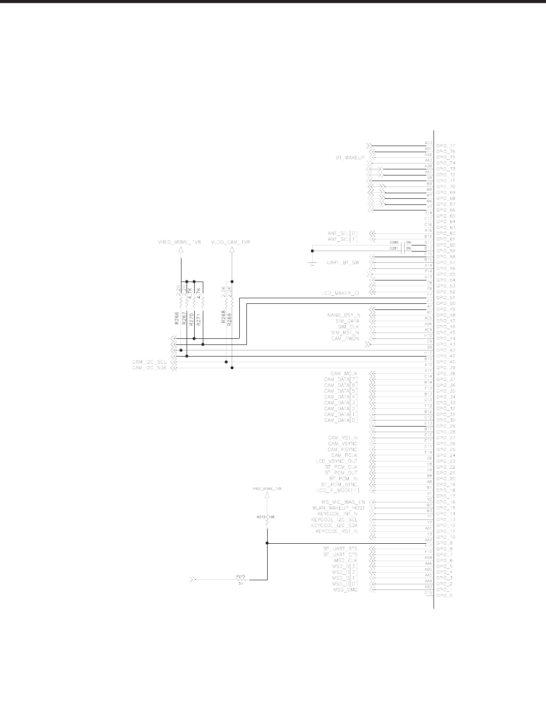
3.1.4 GPIOs
QSC6270 (3G disable has 78 configurable I/O pins
UART_BT_SEL
MUIC_INT_N
CHG_EN_N
BT_WAKEUP_HOST
CHG_STS_N
HALL_SENS_DET
MUIC_AUD_FM_I2C_SCL
MUIC_AUD_FM_I2C_SDA
BL_LCD_CAM_LDO_I2C_SCL
HS_JACK_DET
WLAN_BT_REG_ON
WLAN_CLK
LCD_IF_MODE[0]
BL_LCD_CAM_LDO_I2C_SDA
WLAN_RST_N
BL_LCD_CAM_LDO_EN
BT_RST_N
WLAN_CMD
LCD_RST_N
WLAN_SDIO[3]
WLAN_SDIO[0]
WLAN_SDIO[1]
WLAN_SDIO[2]
BT_PWR_ON
MUSIM_DM
MUSIM_DP
Low : UART Comm
High : BT UART
- 22 -
LGE Internal Use Only Copyright © 2010 LG Electronics. Inc. All right reserved.
Only for training and service purposes
3. TECHNICAL BRIEF
3.1.5 Air interfaces
The supported air-interface standards and features include: (See the RF technical description)
GSM/GPRS/EDGE Specification Release 4 (3GPP R4)
Enhanced GPS position location using gpsOne (with RGR6240 IC)
Integrated gpsOne functionality, featuring enhancements by SnapTrack®, Inc., to enable a wide variety of
location-based services and applications, including points of interest, personal navigation, and friend finder
Simultaneous-GPS (processes GPS using dedicated circuitry while voice and/or data signals continue to be
processed separately)
1024x searcher, direct facility termination (DFT) accelerator, off-chip RAM for measured data storage
3.1.6 Internal base band functions
Several baseband circuits within the QSC6270(3G disable)device provide functions that are necessary only to
make the device operate properly — these functions are not generally used directly by other
handset circuits and functions.
PLLs and clock generation
Modes and resets
Security
Qfuse
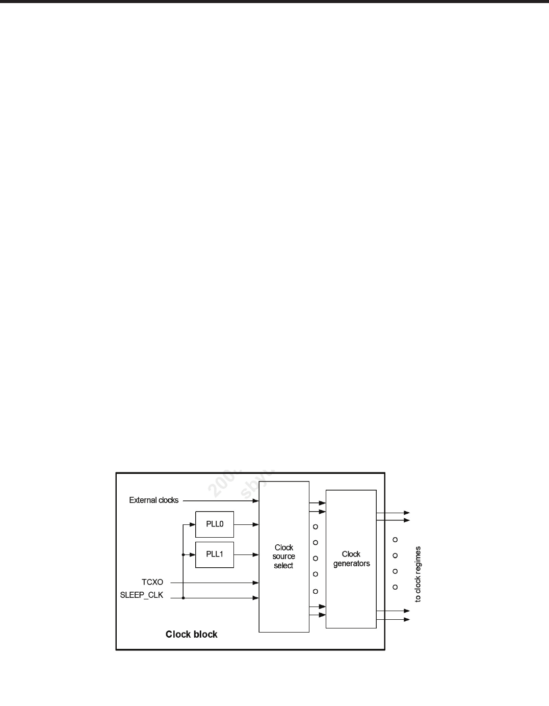
JTAG/ETM
The clock block includes two PLLs, all phase-locked to the TCXO signal. These PLLs generate several
different stable, low-jitter clock signals that are distributed throughout the QSC device and to external c
omponents as needed.
All the required WCDMA, GSM, GPS(only QSC6270), ARM, QDSP, and most peripheral clocks are derived in
some way from the TCXO (or XO) source for their operating modes, plus the 32.768 kHz
oscillator for their sleep modes
Figure 3.1.6 Clock block basic architecture of QSC6270(3G disable)
- 23 -
Copyright © 2010 LG Electronics. Inc. All right reserved.
Only for training and service purposes
LGE Internal Use Only
3. TECHNICAL BRIEF
3.1.7 Multimedia
Multimedia topics are as below in QSC6270, including:
Camera interface and video front-end
Mobile display processor
Additional multimedia support: video, audio, graphics, and messaging
3.1.7.1 Camera interface and video front-end
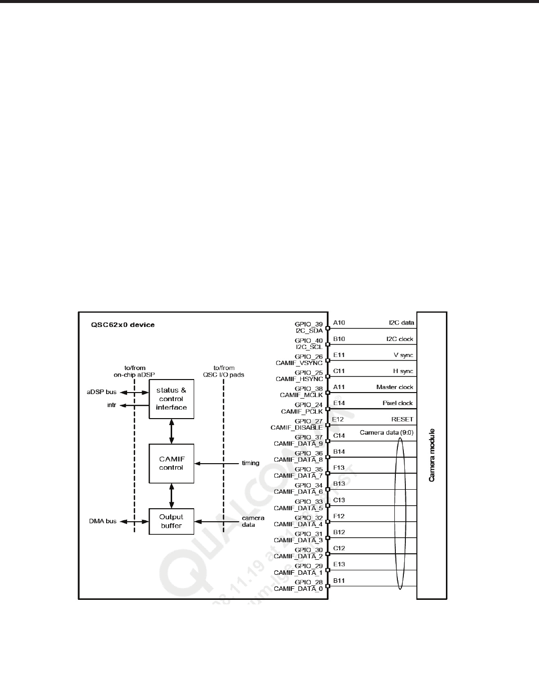
The camera interface (CAMIF) connects the QSC62x0 device directly to a camera sensor. Typical applications
include Qcamera, Qcamcorder, and QvideophoneThe CAMIF delivers the raw 10-bit Bayer pattern data
(preferred) to the video front-end (VFE) that performs the required image processing (RGB-triplet generation,
color-space conversion, auto-white balance, auto exposure, gamma correction, etc.) and prepares the image
for capture or transmission. The QSC device also supports a YUV 4:2:2 input from the sensor
(8-bit, 2:1 MUX YUV or CCIR656 YUV).
The video capabilities of the two QSC devices varies slightly, with the QSC6270 providing higher performance
than the QSC6270 device — greater resolution, higher capture and streaming rates, etc.
- 24 -
LGE Internal Use Only Copyright © 2010 LG Electronics. Inc. All right reserved.
Only for training and service purposes
3. TECHNICAL BRIEF
3.1.7.2 Mobile display processor
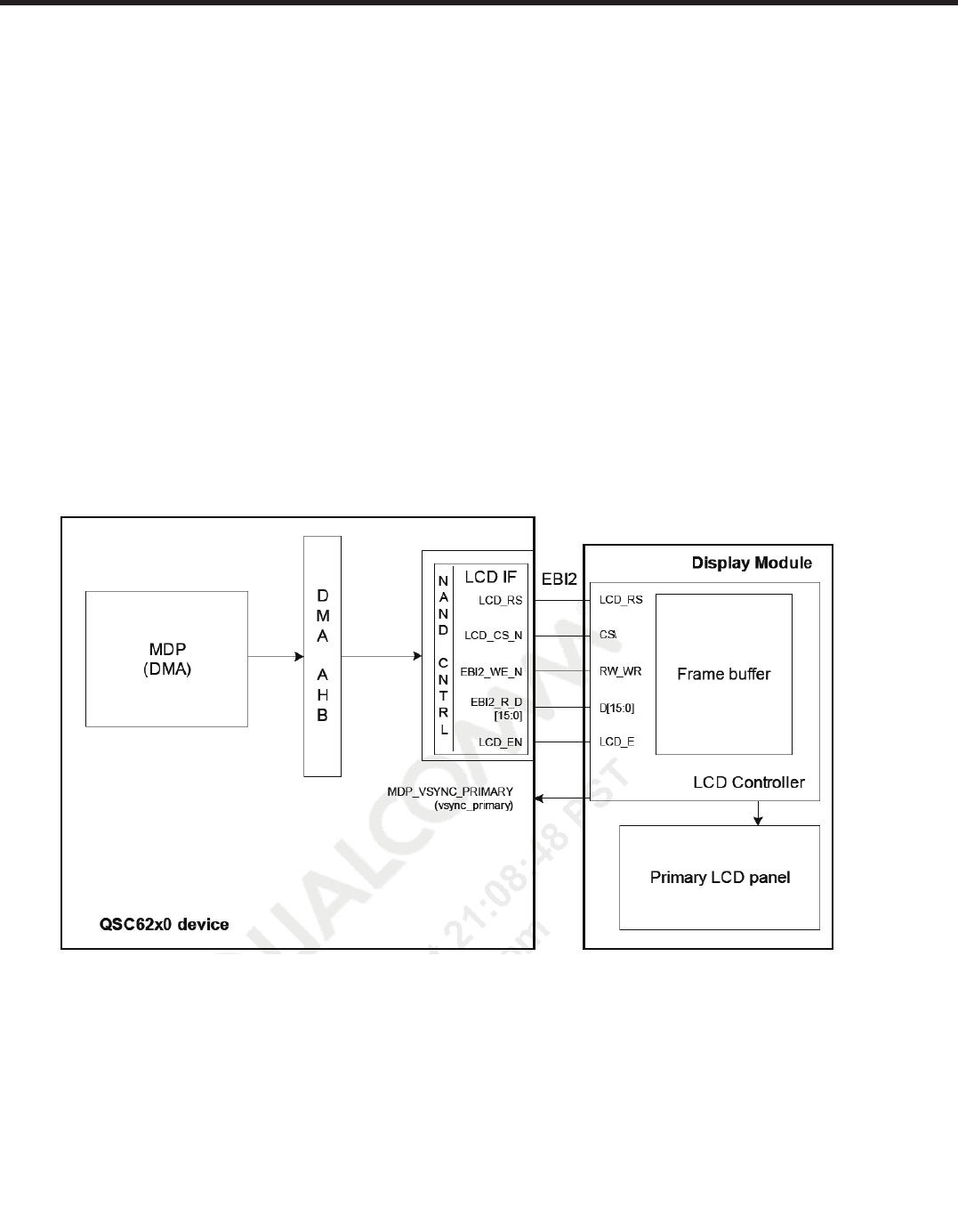
The MDP is a hardware accelerator primarily responsible for transferring an updated image from the QSC
memory subsystem to the LCD module. The transferring of an updated image is an operation that is shared
between software, video processing, and graphics processing, so a common block helps to reduce
redundant circuitry. The MDP is designed with the assumption that the LCD panel has an embedded LCD
controller and a frame buffer. The image transfer is then the copying of the image from the QSC memory
system to the frame buffer within the LCD module.
While the MDP is transferring an image to the LCD module, it can perform a final set of operations to the
image. The set of operations that the MDP can perform has been chosen to maximize the efficiency of the
QSC memory subsystems, typically removing two or more copy operations of the image to and from
memory.
The MDP reduces redundant circuitry and offloads the ARM and aDSP from memory-transfer operations and
a certain set of graphics and video operations
Figure 3.1.7.2.1 MDP-to-LCD interface functional block diagram
- 25 -
Copyright © 2010 LG Electronics. Inc. All right reserved.
Only for training and service purposes
LGE Internal Use Only
3. TECHNICAL BRIEF
Figure 3.1.7.2.2 The LCD interface of C320
C102
0.1u0.1u
C101
CN102
35
34
33
32
31
30
29
28
27
26
25
24
23
22
21
20
19
18
17
16
15
14
13
12
11
10
9
8
7
6
5
4
3
2
1
1
101R
201R 1
VLDO_LCD_1V8 VLDO_LCD_2V8
LCD_MAKER_ID
LCD_RD
WLED3
WLED2
WLED1
LCD_VSYNC_OUT
LCD_RS
LCD_DATA[7]
LCD_DATA[6]
LCD_DATA[5]
LCD_DATA[4]
LCD_DATA[3]
LCD_DATA[2]
LCD_DATA[1]
LCD_DATA[0]
LCD_WR_N
LCD_CS_N
LCD_RST_N
LCD_DATA[15]
LCD_DATA[14]
LCD_DATA[13]
LCD_DATA[12]
LCD_DATA[11]
LCD_DATA[10]
LCD_DATA[9]
LCD_DATA[8]
LCD_IF_MODE[0]
WLED4
WLED5
LCD_IF_MODE[1]
WLED_VOUT

- 26 -
LGE Internal Use Only Copyright © 2010 LG Electronics. Inc. All right reserved.
Only for training and service purposes
3. TECHNICAL BRIEF
3.1.8 UART
̰One universal asynchronous receiver transmitter (UART) port that supports low-speed, full-speed,
and high-speed modes
̰Serial data port communications that conform to the RS-232 interface protocol
̰Used for data transport during Bluetooth operation (BTS402x™ SoC required)
̰Other possible uses:
– Test and debug
– External keypad
– Ringer
– Load/upgrade system software
̰Separate FIFOs for Rx and Tx
̰Supporting circuits include:
– Interrupt control
– Clock source
– Bit-rate generator (BRG)
– Microprocessor interface
̰Flow control is not available on UART2 (behind USIM)
3.1.9 USB
̰Each USB link has a host and a peripheral; the host is responsible for initiating and controlling bus traffic
̰The USB specification requires PCs to act as hosts, and other devices such as printers, keyboards, mice, etc.,
to act as peripherals
̰USB 2.0 implementation defines three modes
- Low-speed (LS): 1.5 Mbps
- Full-speed (FS): 12 Mbps
- High-speed (HS): 480 Mbps
̰The QSC62x0 is compliant with the USB 2.0 specification
- All three modes are supported when acting as a host
- FS and HS are supported when acting as a peripheral
̰The QSC62x0 has two USB controllers
- Primary USB controller
- Secondary USB controller
̰The primary USB controller is supplemented by an integrated physical layer (PHY)
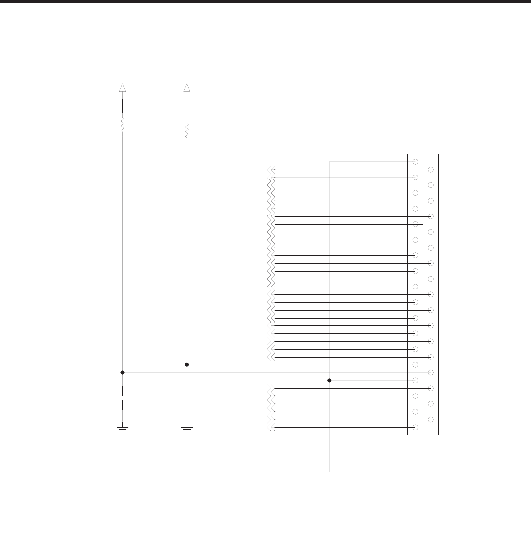
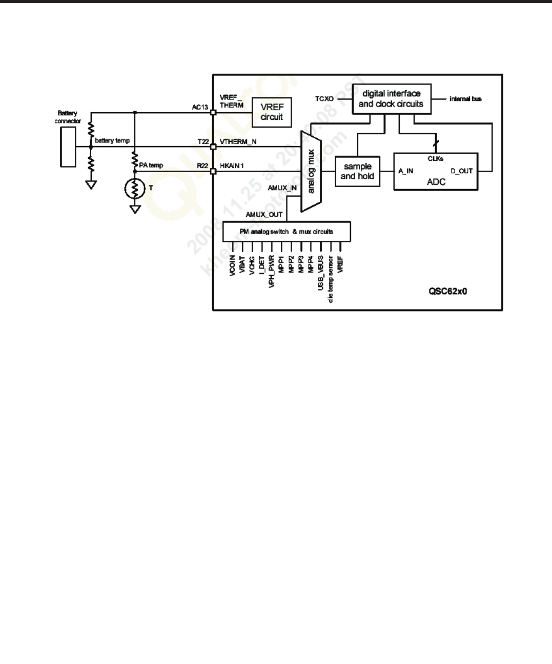
3.1.10 HKADC
The HKADC includes an analog multiplexer that selects an input for the sample and
hold circuit. One of three inputs can be selected:
HKAIN1, pin R22 – an external connection that is available as a general-purpose input,
though it is often used to monitor the power amplifier(s) temperature.
An on-chip connection to the power management circuit’s analog multiplexer output. This allows monitoring of:
-. Key power supply nodes such as VBAT, VCHG, etc.
-. Multipurpose pins (when configured as analog inputs)
-. A few on-chip parameters such as the die temperature or VREF
- 27 -
Copyright © 2010 LG Electronics. Inc. All right reserved.
Only for training and service purposes
LGE Internal Use Only
3. TECHNICAL BRIEF
QSC6270HKADC Block diagram
- 28 -
LGE Internal Use Only Copyright © 2010 LG Electronics. Inc. All right reserved.
Only for training and service purposes
3. TECHNICAL BRIEF
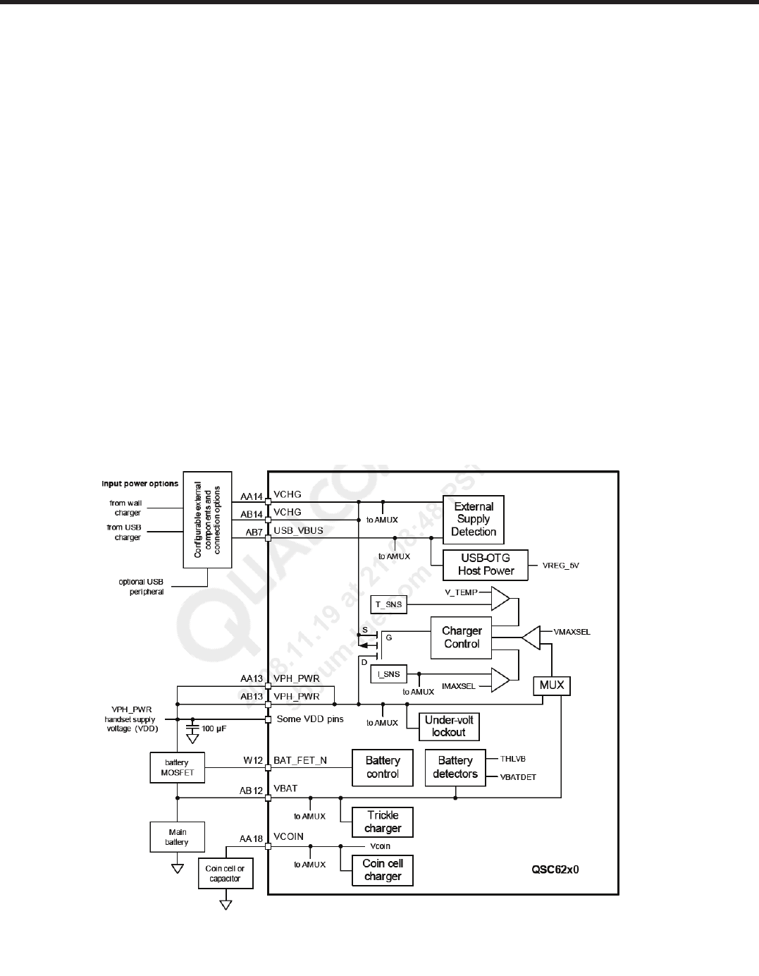
3.2 Power management
3.2.1 Input power management
Valid external supply attachment and removal detection
Unregulated (closed-loop) external charger supply as input power source
Integrated PFET charging pass transistor; eliminated sense resistor
Support for lithium-ion and lithium-ion polymer main batteries; nickel-based batteries are not supported
Trickle, constant current, constant voltage, and pulse charging of the main battery
Autonomous charging option – driven by an on-chip state machine without software intervention
Software-controlled charging option – backwards-compatible with previous QSC and PM products
Coin-cell battery (including charging)
Battery-voltage detectors with programmable thresholds
VDD collapse protection
Charger-current regulation and real-time monitoring for overcurrent protection
Charger-transistor protection by thermal control
Control drivers for the internal charging PFET and external battery PFET
Voltage, current, and thermal control loops
Automated recovery from sudden momentary power loss (requires external32.768 kHz crystal)
Figure 3.2.1 Input circuits schematic diagram

- 29 -
Copyright © 2010 LG Electronics. Inc. All right reserved.
Only for training and service purposes
LGE Internal Use Only
3. TECHNICAL BRIEF
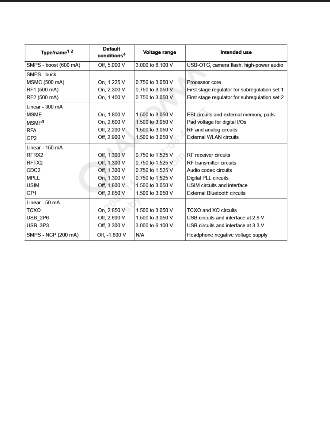
3.2.2 Output voltage regulation
The QSC62x0 device includes all the regulated voltages needed for most low-cost wireless
handset applications (and many other applications). Independent regulated power sources are
required for various electronic functions to avoid signal corruption between diverse circuits,
support power-management sequencing, and meet different voltage-level requirements. Sixteen
voltage regulators are provided — all programmable, all derived from a common bandgap reference circuit.
Three major types of voltage regulator circuits are on-chip:
Three positive voltage switched-mode power supply (SMPS) circuits
- One boost converter (rated for 600 mA)
- Three buck converters (rated for 500 mA each)
Thirteen positive voltage linear regulators
- Four rated for 300 mA
- Six rated for 150 mA
- Three rated for 50 mA
One negative voltage charge pump rated for 200 mA, referred to as a negative charge pump(NCP)
Each regulator has two logic-OR input bits; a logic high at either input enables that regulator:
A master bit that enables all regulators according to their default condition
A dedicated bit that enables only that regulator
The master enable reduces the number of write cycles needed when switching between the phone’s
sleep and active modes.
Additional comments that apply to regulator functions:
If a regulator’s default condition is on, that regulator will power on automatically at QSC startup.
The MSMP regulator must be on to allow internal communications between major functional blocks.
Each regulator and SMPS can provide more than its rated output current, though some
performance characteristics might be degraded.
All regulated output voltages are programmable.
All regulators can be set to a low-power mode except the VREG_USB_3P3 and VREG_NCP circuits
- 30 -
LGE Internal Use Only Copyright © 2010 LG Electronics. Inc. All right reserved.
Only for training and service purposes
3. TECHNICAL BRIEF
Table 3.2.2 Voltage regulator summary
1. All regulator names are based on their intended use, though some may be used to power alternate
functions. For example, the USIM regulator is intended to power an external SIM card but may be used to
power other circuits (or not used at all).
2. Each current listed in this table is its regulator's rated value – the current at which the regulator meets all its
performance specifications. Higher currents are allowed, but higher input voltages may be required and
some performance characteristics may become degraded. See the appropriate regulator sections for details.
3. VREG_MSMP powers key internal circuits and should be kept on at its default voltage setting.
4. All regulators have default output voltage settings, even if they default to an off condition.
- 31 -
Copyright © 2010 LG Electronics. Inc. All right reserved.
Only for training and service purposes
LGE Internal Use Only
3. TECHNICAL BRIEF
3.2.3 Charging control
C320 use single Charger.
- Single charger has five mode like “ OFF / TRICKLE / ISET / USB500 / FACTORY mode”.
- Single Charger is working as ISET mode in case of CC(Constant Current), CV(Constant Voltage) mode,
as USB 500mode in case of USB Charging.
- FACTORY mode is working only for Factory use.
p
j
j
ylT
kGG
kGuv{G
VBUS_LDO_4V9
I
ND
CHG_STS_N
MUIC_IO_M
MUIC_IO_P
MUIC_ACC_ID
- 32 -
LGE Internal Use Only Copyright © 2010 LG Electronics. Inc. All right reserved.
Only for training and service purposes
3. TECHNICAL BRIEF
3.3 SUB SYSTEM
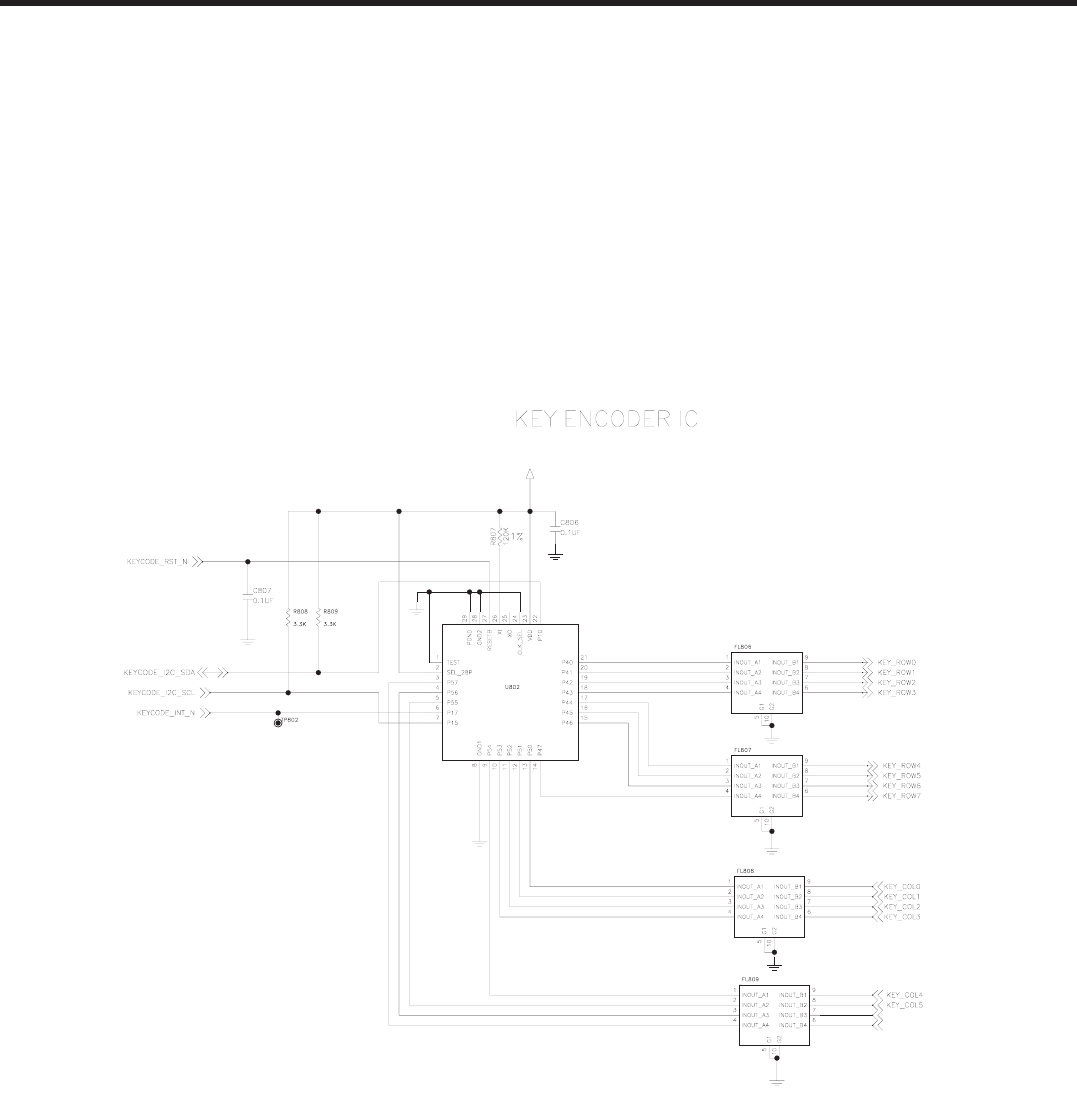
3.3.1 KEY PAD
C320 have a key-coder IC that supports eight sense lines, or columns, and eight keypad rows.
The device scans and encodes 64 matrix – addressed keys on keypads . Key press and release events are stored
in a FIFO buffer with 16 event lengths for uploading to a host processor. The event data stored will indicate the
sequence of events and which keys set pressed or released.
25pF
25pF
25pF
VREG_MSME_1V8
KEY_COL7
KEY_COL6

- 33 -
Copyright © 2010 LG Electronics. Inc. All right reserved.
Only for training and service purposes
LGE Internal Use Only
3. TECHNICAL BRIEF
̰SDRAM
-16-bit low-power DDR SDRAM
-Minimum size per chip-select: 16 MB (128 Mbit)
-Maximum size per chip-select: 128 MB (1 Gbit, 1 k columns only)
Characteristics of the EBI1 clock are listed below:
-Maximum clock rate is 92 MHz, defined by the AMSS software.
-The EBI1 memory controller clock is synchronous to the bus clock (HCLK).
EBI2 Features
EBI2 is used to interface with slower memory and peripheral devices (NAND flash, burst NOR, LCDs, etc.).
The following EBI2 devices are supported:
̰NAND flash
-8/16 bit, single-level cell (SLC)/multi-level cell (MLC) 512/2048-byte page devices
-DMA support
-Boot-up capability from the above devices
̰Burst NOR flash
-16-bit multiplexed AAD burst NOR devices
̰8/16/18-bit (write only) LCD devices (both Motorola and Intel style)
Characteristics of the EBI2 clock are listed below:
̰The maximum clock rate is 46 MHz, defined by the AMSS software.
̰The EBI2 memory controller operates at HCLK/2.
̰Broadcasting and multicasting (QSC6270 only, with MBP1600 IC) are based on:
-Wideband MediaFLO™, DBV-H, and ISDB-T
Asynchronous/burst controller (EBI1 and EBI2)
The external memory controller (xmem_ctlr) forms the asynchronous/burst controller for both EBI1 and EBI2 in
the QSC62x0 device. The controller is generic in terms of its software programmable options and can be
customized when used for EBI1 and EBI2. This block has been enhanced in the QSC62x0 device to support 32-bit
burst memories and byte masking during write operations.
.
3.3.2 External memory interface
The QSC62x0 device has two external bus interface (EBI) ports: EBI1 and EBI2.
EBI1 supports high-speed synchronous dynamic devices. Its memory controller supports the new mobile DDR
SDRAM memories with its higher bandwidth and ability to run at high clock frequencies. This interface supports
the high-bandwidth, high-density, and low-latency requirements of the QSC’s advanced on-chip capabilities
such as the ARM9 processor, highperformance graphics, and video applications.
EBI2 is the slower speed interface intended to support memory devices such as NAND flash and asynchronous
SRAM, peripheral devices such as LCDs, and the UBM receiver for multicast or broadcast reception (QSC6270
only). In addition, EBI2 is required to support a synchronous-burst AAD NOR flash to enable a NOR/DDR SDRAM
memory configuration because the simultaneous mode (NOR, SDRAM) is not supported on the EBI1 bus.
EBI1 Features
EBI1 is a high-performance external memory interface for the QSC62x0 digital block that supports DDR SDRAM
devices Specifically, the following memory devices are supported on EBI1:
- 34 -
LGE Internal Use Only Copyright © 2010 LG Electronics. Inc. All right reserved.
Only for training and service purposes
3. TECHNICAL BRIEF
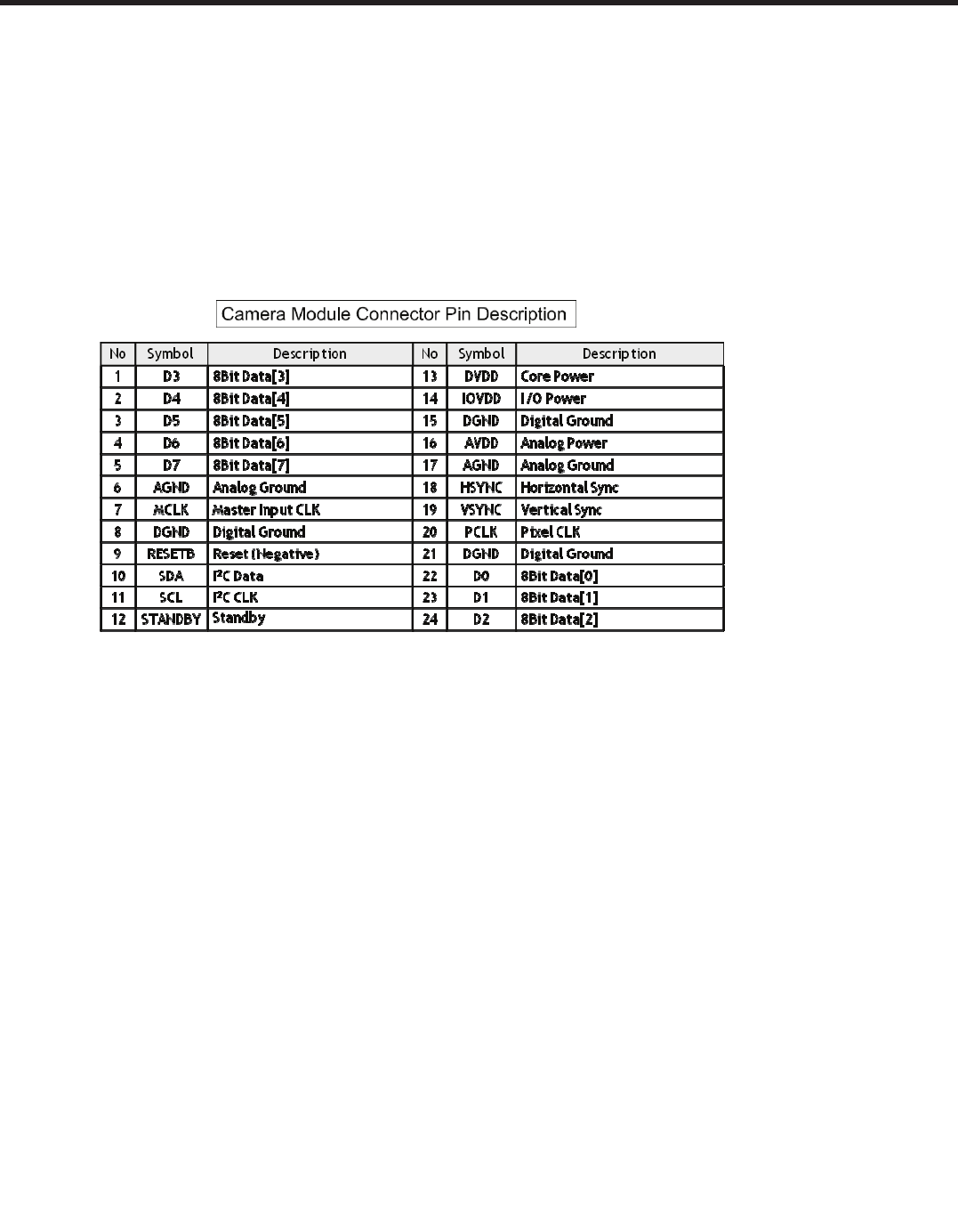
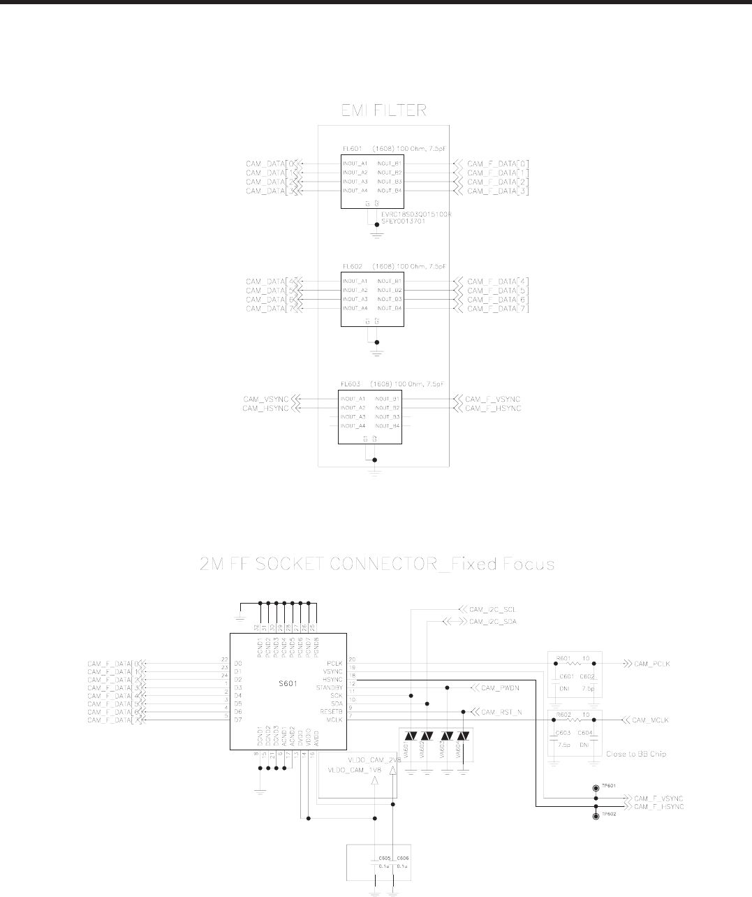
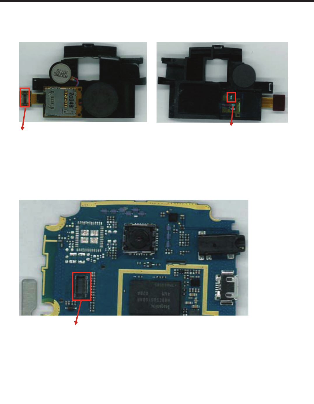
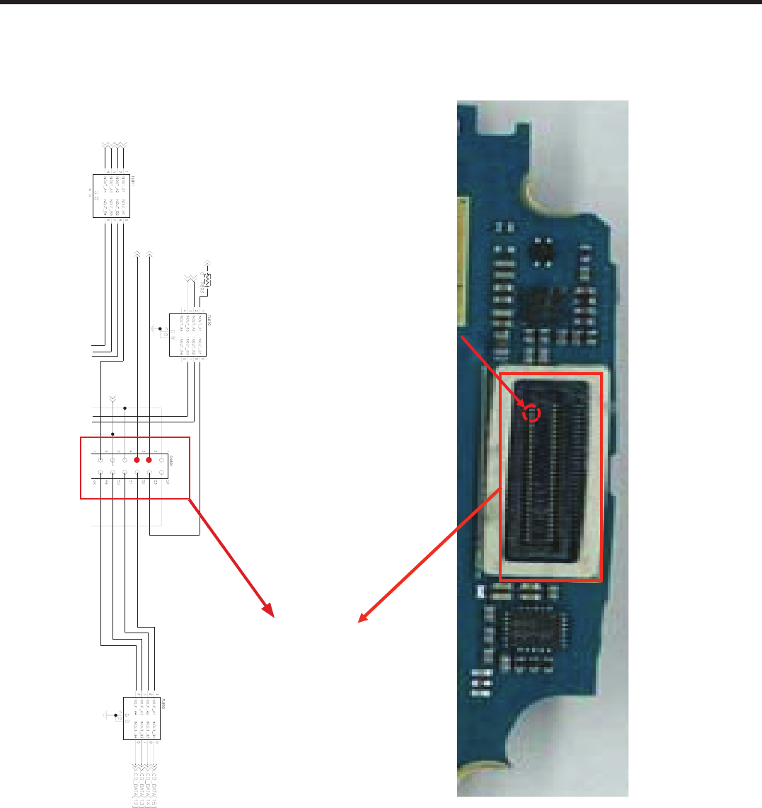
3.3.3 Camera Interface ( 2M CAMERA )
3.3.3.1 2M CAMERA
C320 Installed a 2M Pixel Camera. Below picture shows the camera board to board connector and
camera I/F signal.
- 35 -
Copyright © 2010 LG Electronics. Inc. All right reserved.
Only for training and service purposes
LGE Internal Use Only
3. TECHNICAL BRIEF
01
5
64
73
82
91
01
5
64
73
82
91
01
5
64
73
82
91
- 36 -
LGE Internal Use Only Copyright © 2010 LG Electronics. Inc. All right reserved.
Only for training and service purposes
3. TECHNICAL BRIEF
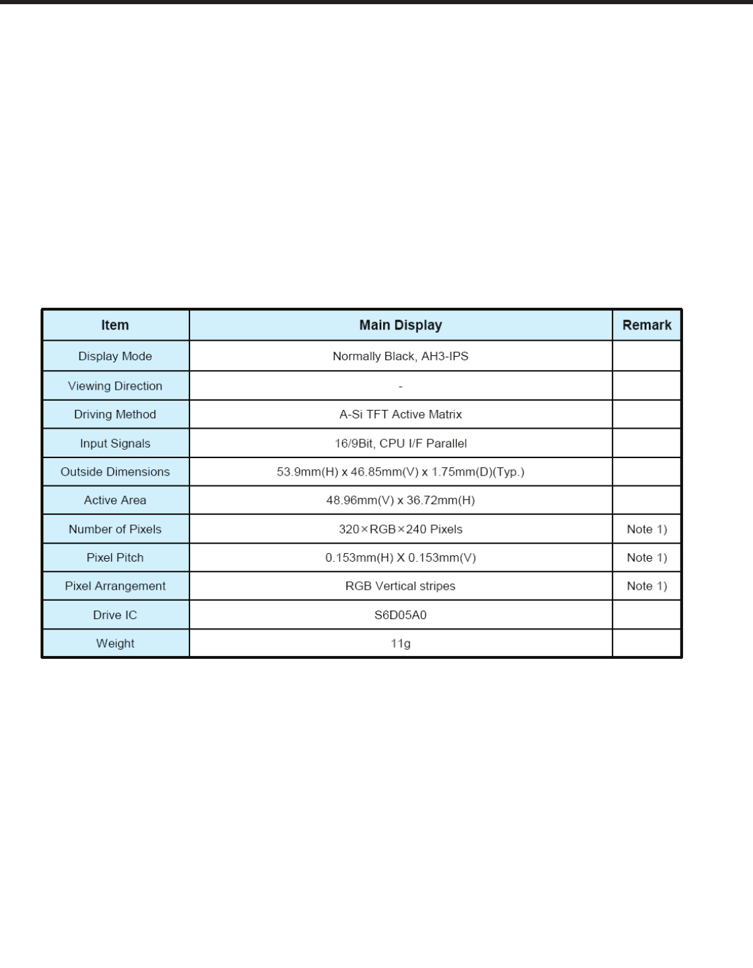
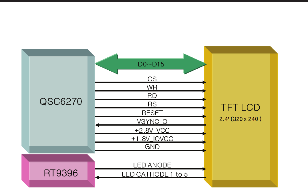
3.3.4 LCD Module (LQ024Q3UX01 : SHARP)
The DM24-DSM04 model is a Color TFT LCD supplied by LG Innotek.
This main Module has a 2.4 inch diagonally measured active display area with 320(RGB) X 240 resolution.
Each pixel is divided into Red, Green and Blue sub-pixels and dots which are arranged in vertical stripes.
Main LCD color is determined with 262k colors signal for each pixel.
The DM24-DSM04 has been designed to apply the interface method that enables low power, high speed, and
high contrast. The DM24-DSM04 is intended to support applications where thin thickness and low power are
critical factors and graphic displays are important
GENERAL DESCRIPTION
- 37 -
Copyright © 2010 LG Electronics. Inc. All right reserved.
Only for training and service purposes
LGE Internal Use Only
3. TECHNICAL BRIEF
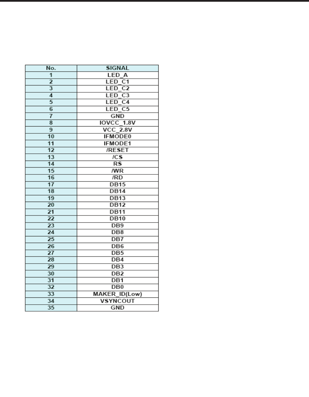
Input Signal and Power : Pin Description ( Input Pin : 35 )
PIN DESCRIPTION
- 38 -
LGE Internal Use Only Copyright © 2010 LG Electronics. Inc. All right reserved.
Only for training and service purposes
3. TECHNICAL BRIEF
- 39 -
Copyright © 2010 LG Electronics. Inc. All right reserved.
Only for training and service purposes
LGE Internal Use Only
3. TECHNICAL BRIEF
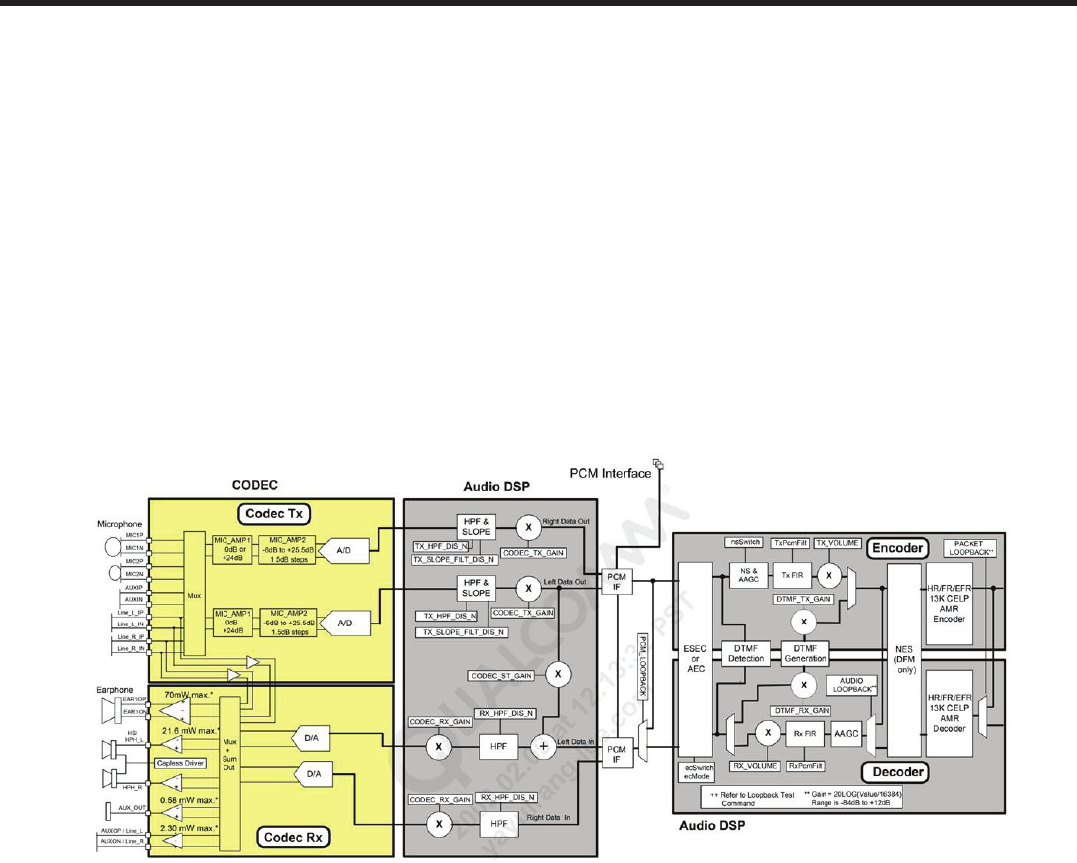
3.3.5 Audio Signal Processing & Interface
Audio signal processing is divided uplink path and downlink path. The uplink path amplifies the audio signal
from MIC and converts this analog signal to digital signal and then transmits it to DBB Chip (QSC6270). This
transmitted signal is reformed to fit in GSM & WCDMA frame format and delivered to RF Chipset. The downlink
path amplifies the signal from DBB chip (QSC6270) and outputs it to receiver (or speaker).
The receive path can be directed to either one of two earphone amplifiers or the auxiliary output. The outputs
earphone1 (EAR1OP, EAR1ON) and auxiliary out (LINE_OP, LINE_ON) are differential outputs. Earphone2 (HPH_L,
HPH_R) is a single-ended output stage designed to drive a headset speaker. The microphone interface consists
of two differential microphone inputs, one differential auxiliary input and a two-stage audio amplifier.
- 40 -
LGE Internal Use Only Copyright © 2010 LG Electronics. Inc. All right reserved.
Only for training and service purposes
3. TECHNICAL BRIEF
G
3.4 GENERAL DESCRIPTION
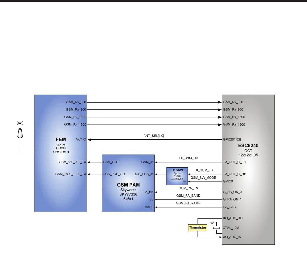
The RF platform of C320 supports four communication bands (GSM850 / GSM900 / GSM1800 / GSM1900).
The all the RF blocks can be divided into two main parts, which are a GSM, and an antenna switch Mode.
The simplified block diagram is shown in Figure 3.4
[Figure 1.1] Block diagram of RF part
(RF Part)
3.4

- 41 -
Copyright © 2010 LG Electronics. Inc. All right reserved.
Only for training and service purposes
LGE Internal Use Only
3. TECHNICAL BRIEF
G
3.5 GSM MODE
The EDGE/GPRS/GSM transceiver use a digital interface that is shared between receive and transmit data.
The receive interface is based on I and Q data and the transmitter interface is based on envelop and
frequency data.
The quad band EDGE/GSM/GPRS transceiver has the following general features:
Power class
GMSK low bands: Class 4 (33 dBm)
GMSK high bands: Class 1 (30 dBm)
8PSK low bands: Class E2 (27 dBm)
8PSK high bands: Class E2 (26 dBm)
Multi slot class 12 (4+4=5)
Dual Transfer Mode (DTM) class 9 (3+2=5)
Zero-IF receiver
-Polar modulation transmitter
3.5.1 GSM RECEIVER
The RF receiver designs are leveraged from previous-generation RTR devices, including the latest innovations.
All ESC receiver paths are discussed in this section.
The ZIF receive signal paths support multiband, multimode applications:
Quad-band GSM:
Low-band
GSM 850 (869 to 894 MHz) and GSM 900 (925 to 960 MHz)
High-band
DCS1800 (1805 to 1880 MHz) and PCS1900 (1930 to 1990 MHz)
The on-chip receive signal paths are functionally identical for each mode (GSM or EDGE) and each band type
(low or high). The external circuitry includes the antenna switch module and a filter function.
All RF Rx inputs use a differential configuration to maximize common-mode rejection, Tx isolation, out-of-
band suppression, and second-order intermodulation performance. The first of two quadrature
downconverters accepts inputs from two LNAs (only one is active at a time). An example application could
support the following bands using these two LNAs:
GSM 1900
GSM 850
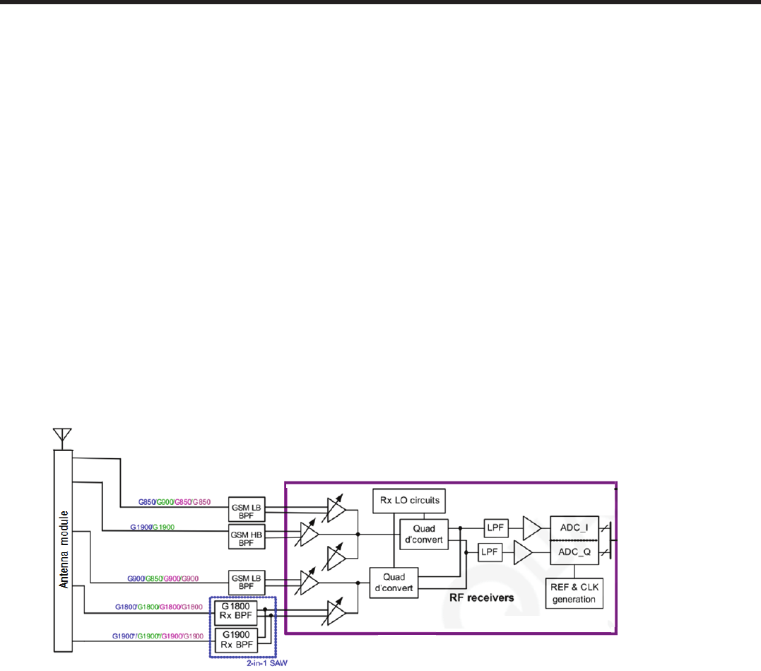
- 42 -
LGE Internal Use Only Copyright © 2010 LG Electronics. Inc. All right reserved.
Only for training and service purposes
3. TECHNICAL BRIEF
G
The second downconverter accepts inputs from another two LNAs (again, just one is active at time) and is
dedicated to GSM 900 and GSM 1800 operation.
The two downconverter outputs drive analog baseband filters and buffer circuits that are programmed to
support the active operating mode’s waveforms (GSM or EDGE). The analog baseband signals are then
digitized by analog-to-digital converters (ADCs) whose outputs are routed to the digital baseband circuits for
further processing.
Numerous secondary Rx functions are also integrated: Rx frequency synthesizers (each having their own PLL
and VCO circuits), LO generation and distribution circuits, reference and clock circuits for the ADCs, and
various interface, control, and status circuits. Power reduction features (such as selective circuit powerdown,
gain control, and bias control) extend handset standby time.
Like the Tx LO, all Rx LO circuits are completely integrated. All received LO signals are generated by the on-
chip Rx VCOs under control of their PLLs.
[Figure 3.5.1] QSC GSM receiver signal paths functional diagram
- 43 -
Copyright © 2010 LG Electronics. Inc. All right reserved.
Only for training and service purposes
LGE Internal Use Only
3. TECHNICAL BRIEF
G
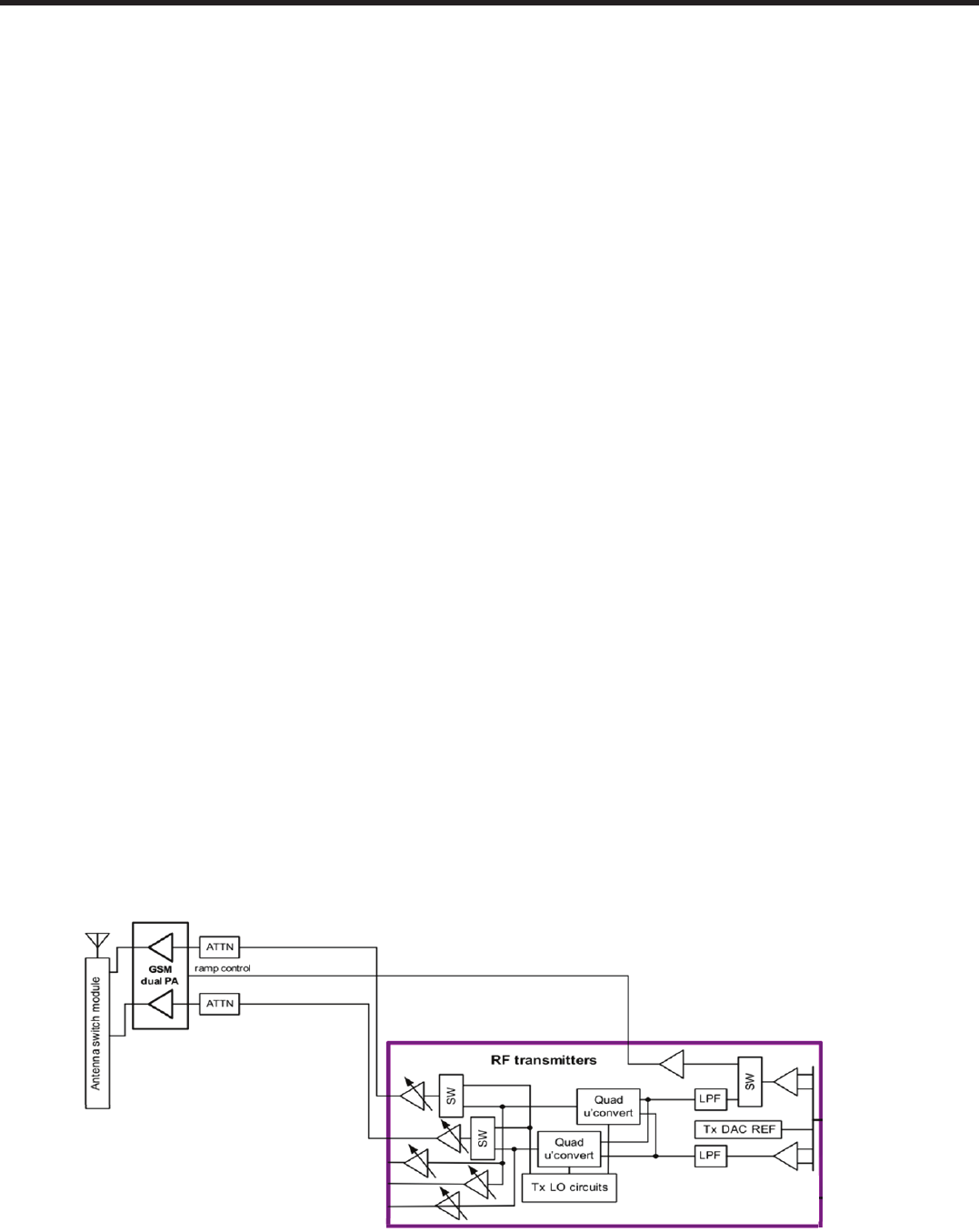
3.5.2 GSM TRANSMITTER
The RF transmitters are leveraged from previous-generation RTR™ devices, including the latest innovations.
The ESC transmitter paths and Tx power-detector input are discussed in this section. It provides the zero-IF
(ZIF) transmit signal paths for multiband, multimode applications:
Quad-band GSM:
Low-band
GSM 850 (869 to 894 MHz) and GSM 900 (925 to 960 MHz)
High-band
DCS1800 (1805 to 1880 MHz) and PCS1900 (1930 to 1990 MHz)
The transmit signal paths include a shared set of baseband amplifiers, a dedicated quadrature upconversion
for each band-type (low and high), gain control RF amplification, and multiple output driver amplifiers for
each band-type. Two GSM output drivers support one low-band and one high-band type (but each GSM
band-type is dual-band). The GSM transmitters in polar PA configuration are also supported by a PA envelope
control path, plus the ability to route LO signals to the transmit chains for test and calibration purposes. In
linear PA configuration, phase and envelope paths are combined inside the ESC and amplified using a
multistage linear PA.
Numerous secondary Tx functions are also integrated: a reference for the transmit DACs, the Tx phase-locked
loop (PLL), the Tx OSC circuit, the Tx LO generation and distribution circuits, an RMS Tx power detector, and
various interface, control, and status circuits.
The RF transmitter interfaces internally with the baseband circuits for its analog baseband input and status
and control signaling. Power reduction features controlled by baseband circuits (such as selective circuit
powerdown, gain control, and transmit puncturing) extend handset talk time. The driver amplifier outputs
are routed externally to the final stages of the transmit chains, culminating with the antenna switch whose
output drives the antenna.
Sophisticated Tx LO circuits implement the frequency plan and are completely integrated on-chip. All Tx LO
signals are generated by the on-chip Tx OSC under the control of its PLL.
[Figure 3.5.2] QSC GSM transmitter signal paths functional diagram
- 44 -
LGE Internal Use Only Copyright © 2010 LG Electronics. Inc. All right reserved.
Only for training and service purposes
3. TECHNICAL BRIEF
G
3.6 OFF-CHIP RF COMPONENTS
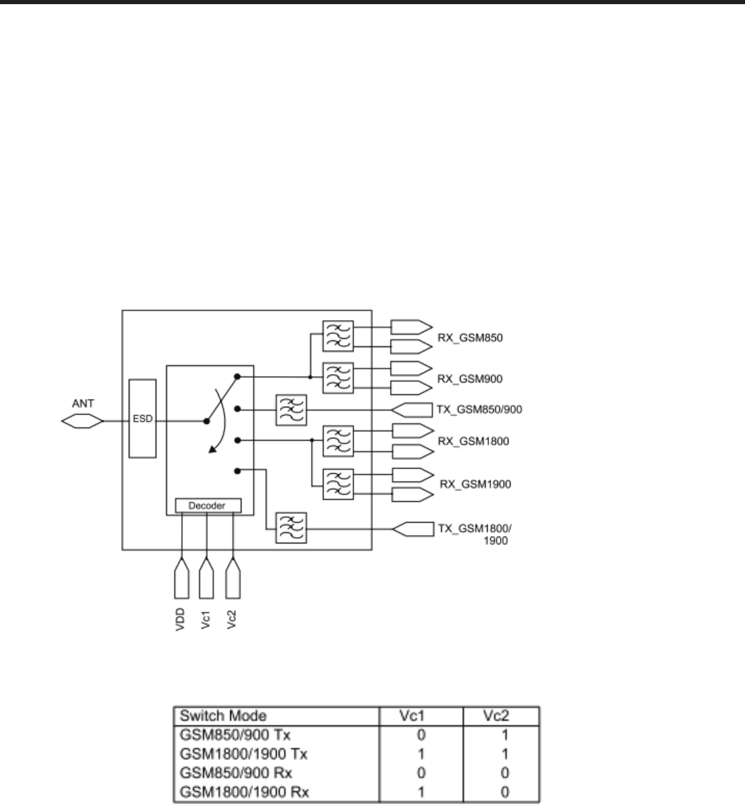
3.6.1 D5008 (FL101: FEM)
Low-loss SAW frontend module for mobile telephone system
Covering GSM850, GSM900, GSM1800 and GSM1900 bands
Integration of Tx low pass filters, switch, de-coder and diplexing network between GSM Filters
Integration of GSM850, GSM900, GSM1800 and GSM1900 Rx SAWs
Balanced outputs of all Rx ports
Integration of ESD protection at Ant port to 8kV acc. IEC-61000-4-2 (contact discharge)
[Figure 3.6.1] Block diagram of FEM
[Table 3.6.1] Control table of FEM
- 45 -
Copyright © 2010 LG Electronics. Inc. All right reserved.
Only for training and service purposes
LGE Internal Use Only
3. TECHNICAL BRIEF
G
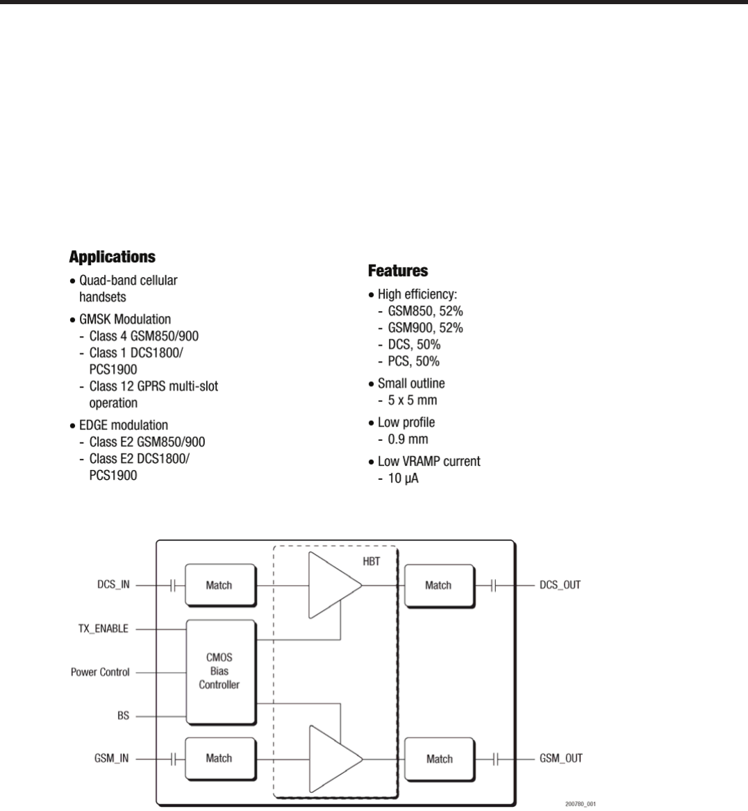
3.6.2 GSM850/EGSM/DCS/PCS Dual band Transmit Power Amplifier
(U101: SKY77336)
The dual band PA is operating to transmit for low band (GSM-850, GSM-900) and high band (GSM-1800,
GSM1900). Operating mode is selected and controlled by the ESC6270 (GSM_PA_BAND).
[Figure 3.6.2] Block diagram of GSM PAM
- 46 -
LGE Internal Use Only Copyright © 2010 LG Electronics. Inc. All right reserved.
Only for training and service purposes
3. TECHNICAL BRIEF
G
3.7 OFF-CHIP COMPONENTS
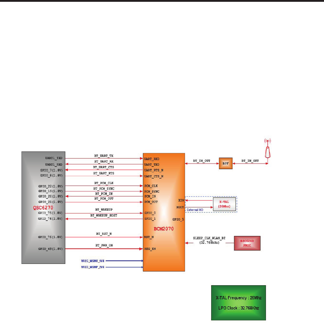
3.7.1 Bluetooth (BCM2070)
Bluetooth block of LG-C320 consists of a BCM2070 chip-set, an external crystal oscillator(26MHz), and a
Bluetooth chip antenna (2.4GHz). QSC6270_3G disable, which is main HW solution of LG-C320 Model, doesn’t
include BT baseband core. Instead, Bluetooth chipset, BCM2070, contains stand-alone baseband processor
(V2.1+EDR) as well as BT RF block. An external crystal oscillator (26MHz) is used to provide reference
frequency to BCM2070.
Figure 3.7 shows the Bluetooth system architecture in the LG-C320.
[Figure 3.7] Bluetooth system architecture
- 47 -
Copyright © 2010 LG Electronics. Inc. All right reserved.
Only for training and service purposes
LGE Internal Use Only
3. TECHNICAL BRIEF
G
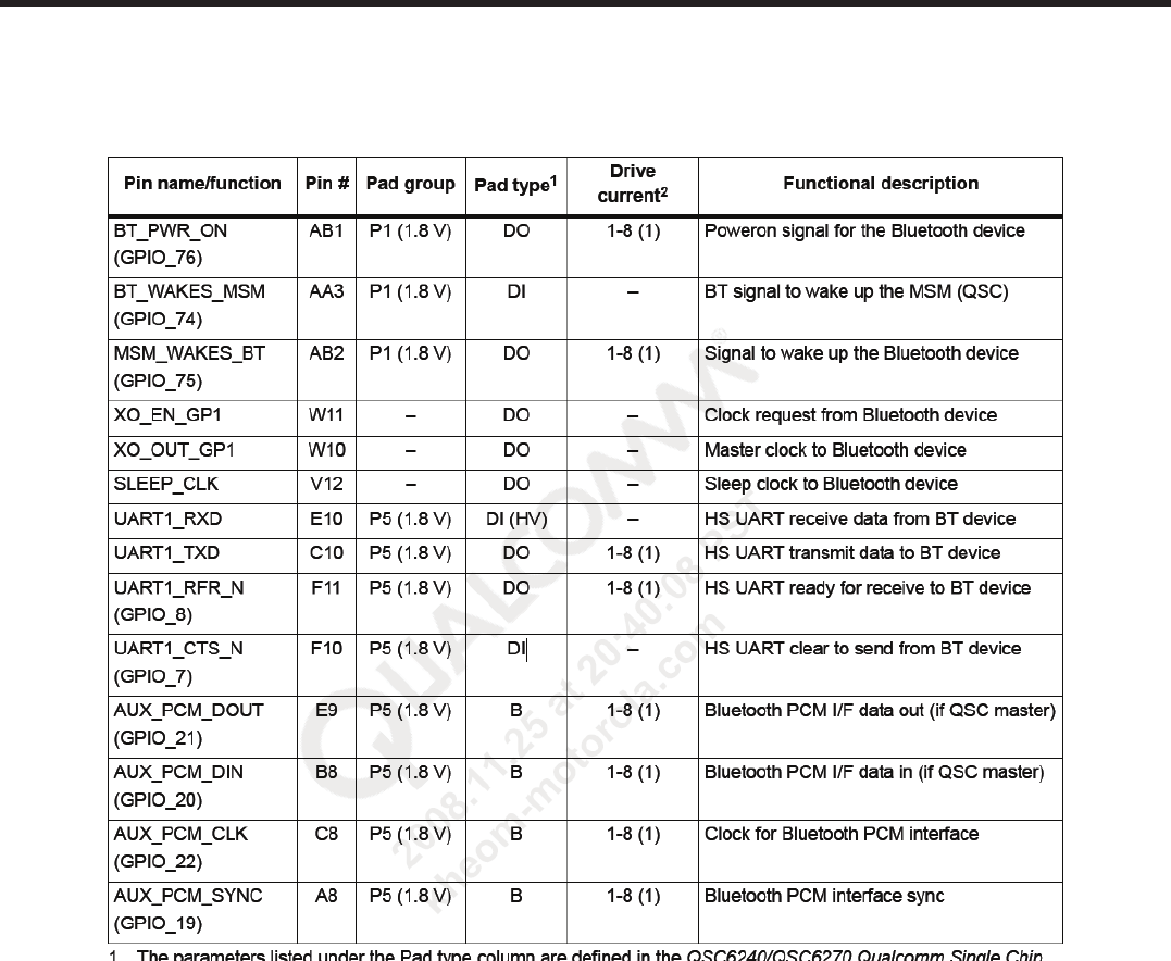
[Table 3.7] Bluetooth Connection(GPIO) with QSC6270
- 48 -
LGE Internal Use Only Copyright © 2010 LG Electronics. Inc. All right reserved.
Only for training and service purposes
3. TECHNICAL BRIEF
G
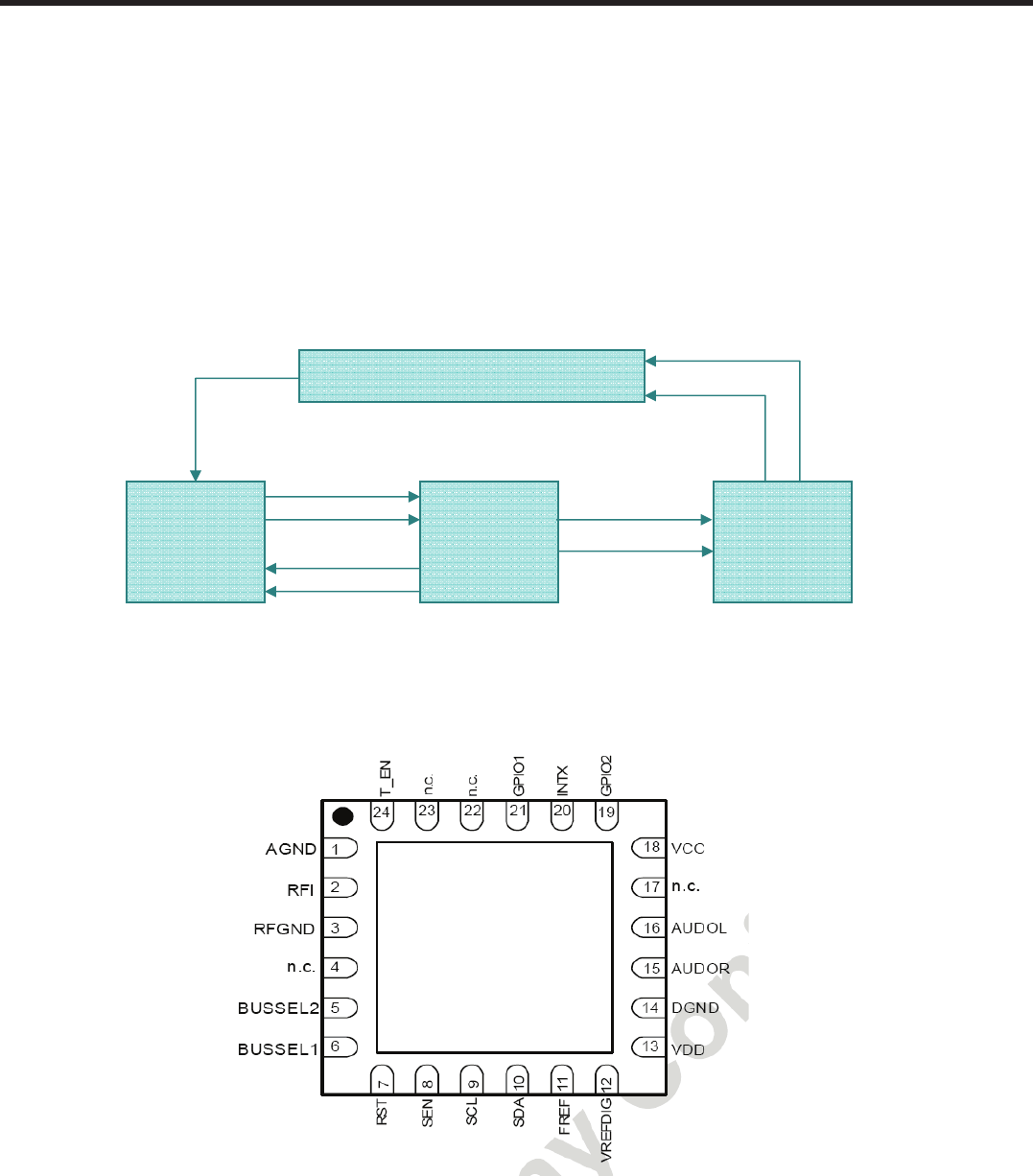
3.7.2 FM Receiver (TEA5991)
The TEA5991 is a single chip FM stereo radio with RDS and RBDS decoder. The radio can be connected to a
headphone antenna and can tune from 70-108 MHz to cover the European, US, Chinese and Japanese FM
band. The radio delivers stereo audio output to an external amplifier. The radio can be controlled with a high
level command based interface through a I2C or SPI-bus.
[Figure3.7.2] shows the FM Radio system architecture in the LGC320.
[Figure3.7.2] FM Radio system architecture
[Figure3.7.2.1] Pin Descriptions
G
ESC6270
AUDIO
SUBSYSTEM
FM
TEA5991
FM_R
FM_L
FM_I2C_SDA
FM_I2C_SDL
HP_R
HP_L
Ear-Jack
FM_ANT
HP_EAR_R
HP_EAR_L
- 49 -
Copyright © 2010 LG Electronics. Inc. All right reserved.
Only for training and service purposes
LGE Internal Use Only
3. TECHNICAL BRIEF
G
SYMBOL HVQFN WLCSP DESCRIPTION
AGND 1 F1 Analog ground
RFI 2 E1 RF input
RFGND 3 D1 RF ground
NC 4 - not connected
BUSSEL2 5 A1 Bus Selection pin 2
BUSSEL1 6 C1 Bus Selection pin 1
RST 7 A2 Reset, used for operating mode change
SEN 8 B1 Chip Select for SPI bus
SCL 9 A3 Serial Bus Clock
SDA 10 A4 Serial Bus Data
FREF 11 A5 Reference frequency (32.768 kHz)
VREFDIG 12 A6 Reference voltage for digital I/Os
VDD 13 B6 Digital supply voltage
DGND 14 C6 Digital ground
AUDOR 15 D6 Audio output signal right
AUDOL 16 E6 Audio output signal left
NC 17 - Not connected
VCC 18 F6 Analog supply voltage
GPIO2 19 F5 General Purpose I/O 2; Dataout for 4-wire SPI-bus
[Table 3.7.2] pin description
- 50 -
LGE Internal Use Only Copyright © 2010 LG Electronics. Inc. All right reserved.
Only for training and service purposes
4. TROUBLE SHOOTING
4. TROUBLE SHOOTING
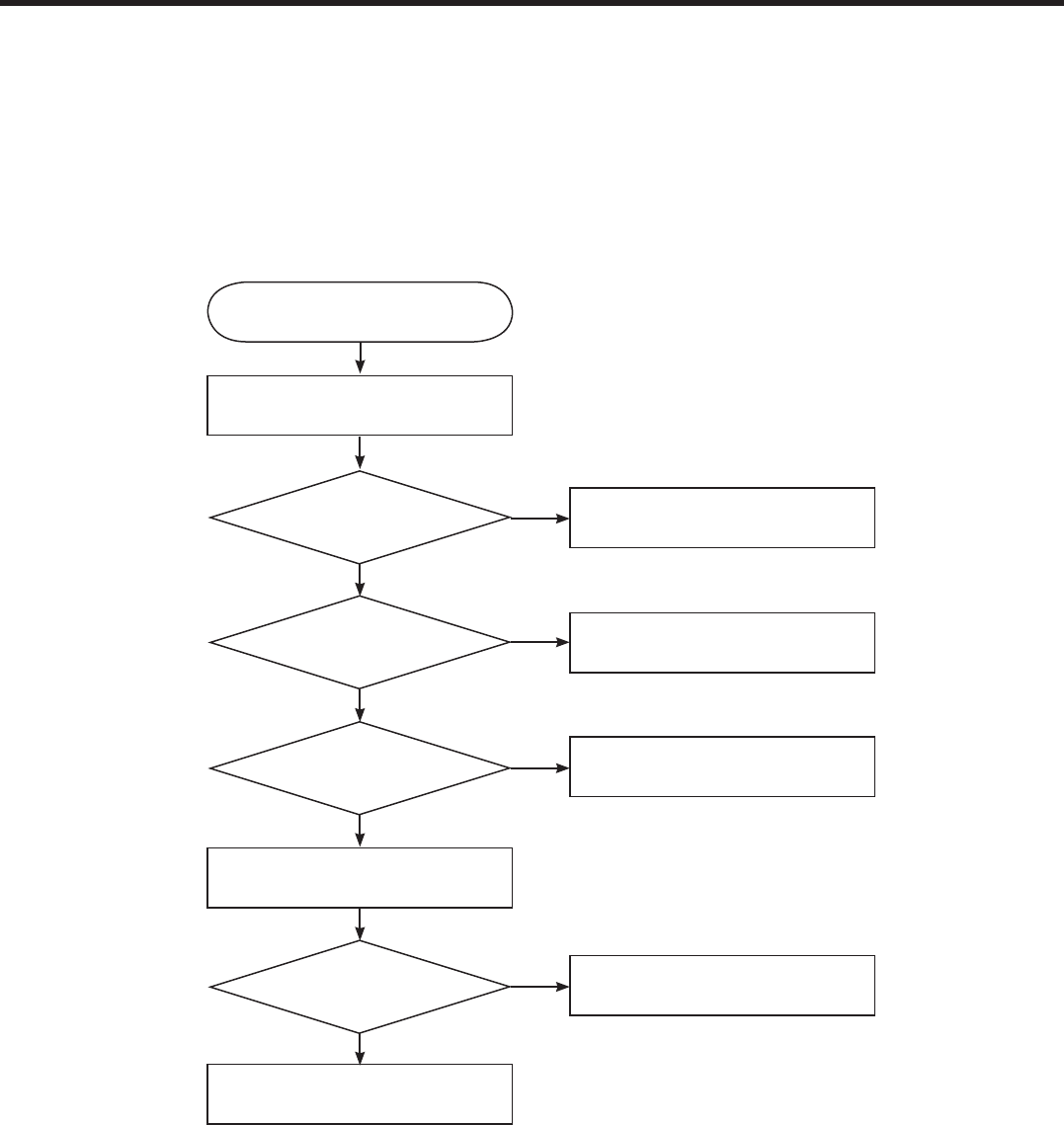
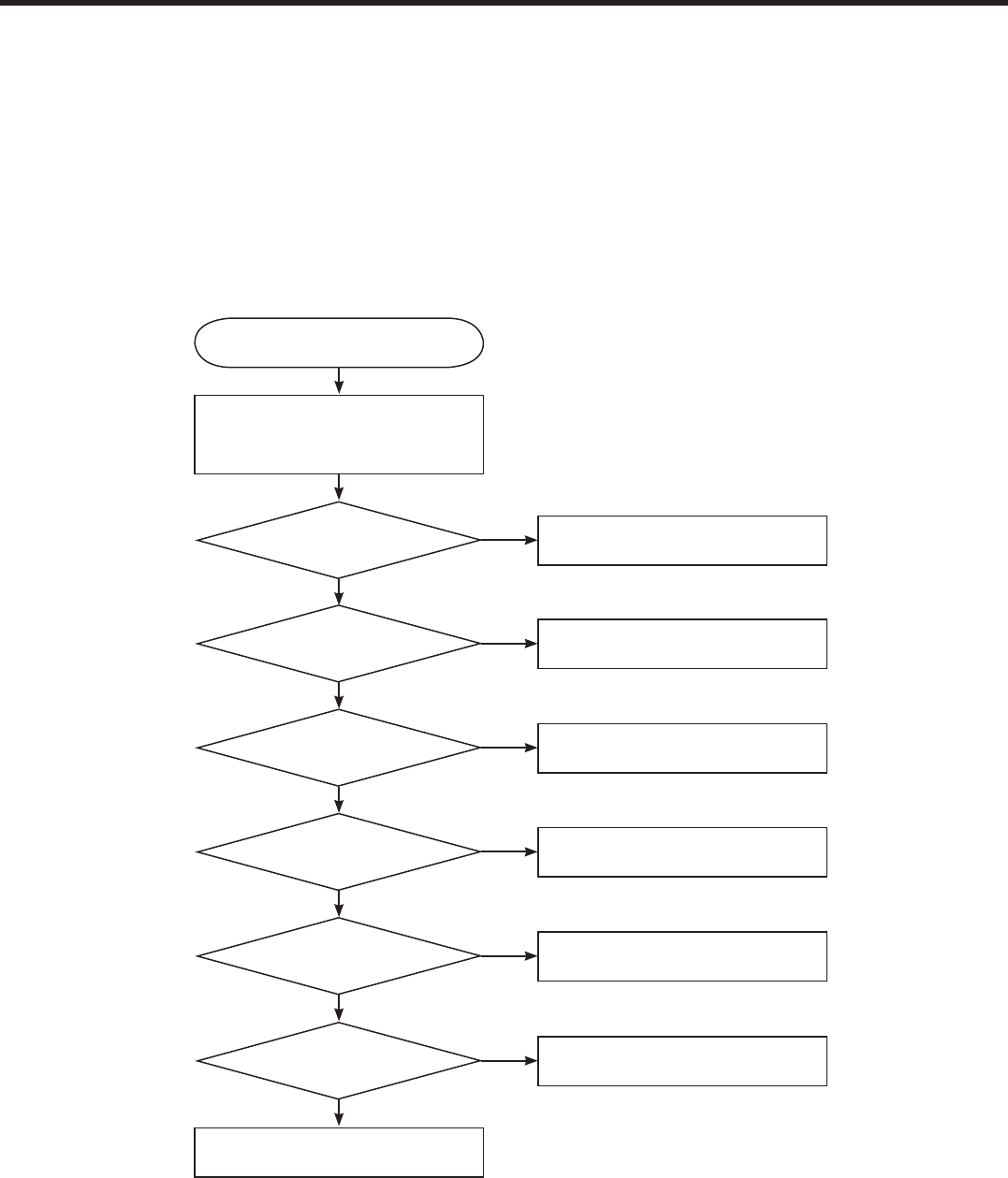
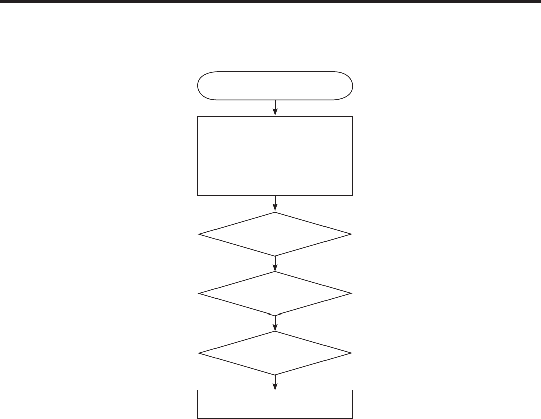
Power ON Troubleshooting
5. Base band part
4.1 Power ON Troubleshooting
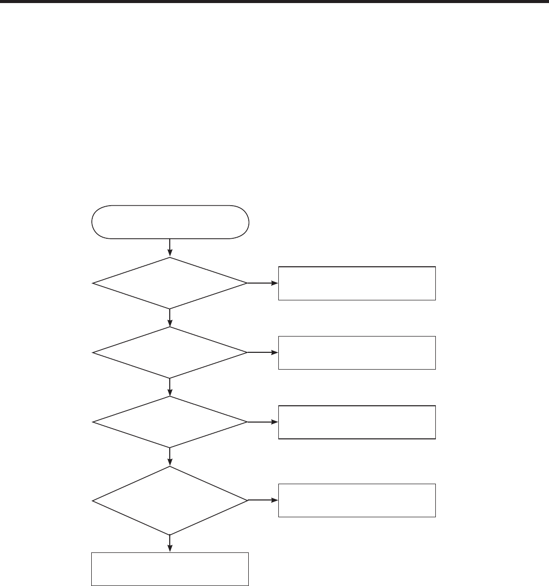
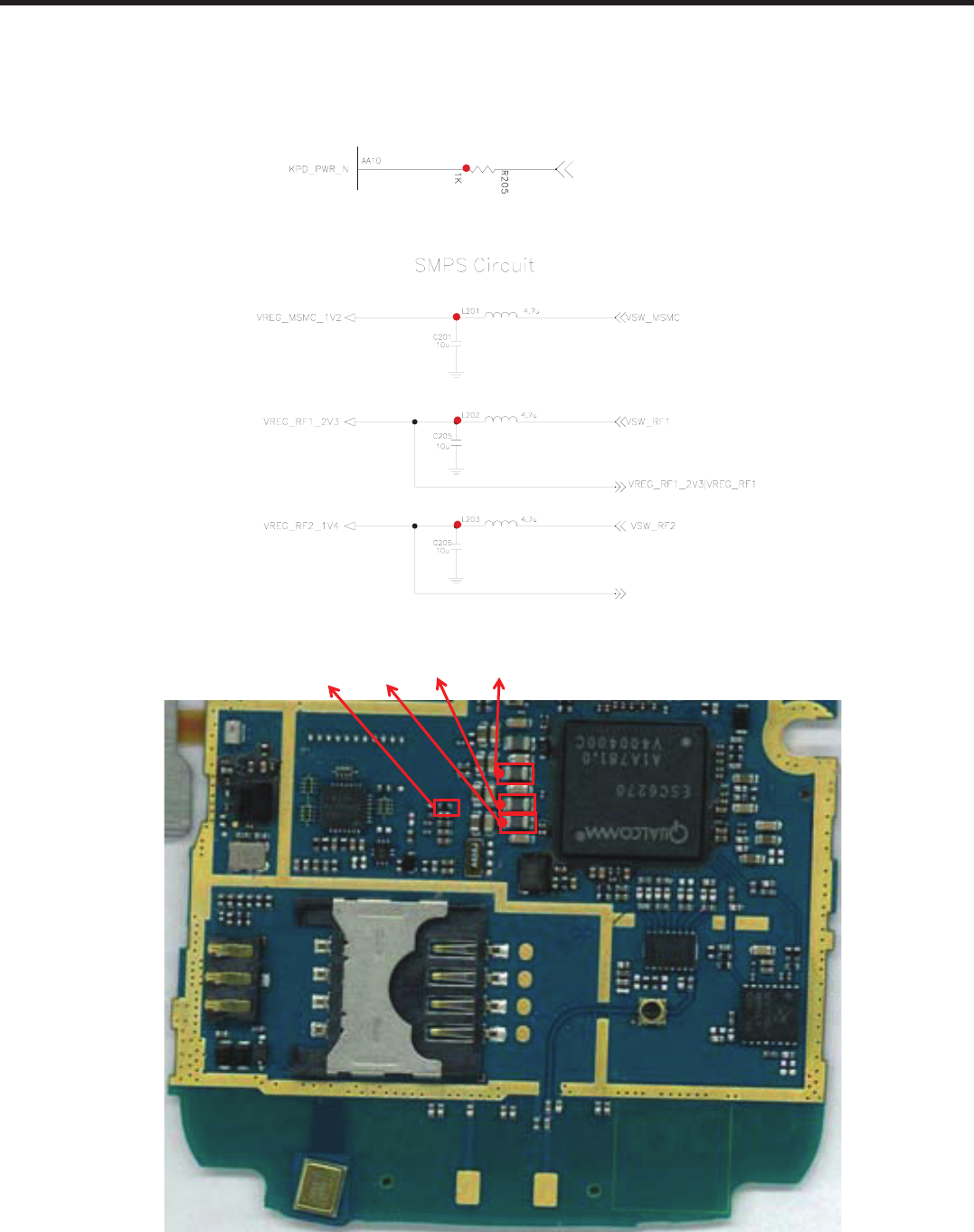
Power On sequence is :
PWR key press PM_ON_SW_N ÎQSC6270 KPDPWR_N pin(AA2) go to low(Main BOARD R205) ÎQSC6270
Power Up ÎVREG_MSMC_1.2V(C261), VREG_MSME_1.8V(C209), VREG_MSMP_2.6V(C414),
VREG_RFRX2_1.3V(C232), VREG_TCXO_2.85V(C275) power up and system reset assert to QSC6270 ÎPhone
booting and PS_HOLD assert to QSC6270
START
Battery voltage. higher
than 3.20V? Change or charging the Battery
No
Yes
Change the main board
Replaced
with normal LCD module,
and then Booting is OK? Go to LCD Troubleshooting
Yes
No
TP1_R205 go to low
When Power key press? Check the Key Dome
No
Yes
TP2_VREG_MSMC_1.2V(L201)
TP3_VREG_RF1_2.3V(L202)
TP4_VREG_RF1_1.4V(L203)
power up?
Change the main board
No
Yes
- 51 -
Copyright © 2010 LG Electronics. Inc. All right reserved.
Only for training and service purposes
LGE Internal Use Only
4. TROUBLE SHOOTING
Power ON Troubleshooting
TP3TP4TP2TP1
VREG
_
RF2
_
1V4
|
VREG
_
RF2
N
_W
S
NO_MP
TP1
TP2
TP3
TP4
- 52 -
LGE Internal Use Only Copyright © 2010 LG Electronics. Inc. All right reserved.
Only for training and service purposes
4. TROUBLE SHOOTING
൯Charging Procedure
- Connect TA or USB Cable
- Control the charging current by QSC6270(disable 3G)
- Charging current flows into the battery
තCheck Point
- Connection of TA or USB Cable
- Charging current path
- Battery
තTroubleshooting Setup
- Connect TA and battery to the phone
තTroubleshooting Procedure
- Check the charger (TA or USB Cable) connector
- Check the charging current Path
- Check the battery
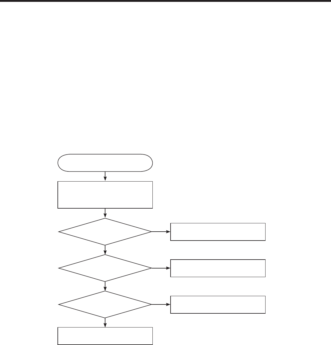
4.2 Charger Troubleshooting
Charger Troubleshooting
Check the pin and battery
Connect terminals of I/O
connector
Connection OK? Change I/O connector
No
Yes
Change the main board
Is the TA voltage TP1_5.1V(FL401)? Change TA
No
Yes
Is it charging properly? END
Yes
No
START
[ Charger Troubleshooting Flow ]
- 53 -
Copyright © 2010 LG Electronics. Inc. All right reserved.
Only for training and service purposes
LGE Internal Use Only
4. TROUBLE SHOOTING
Charger Troubleshooting
FL401
TP1
TP1
- 54 -
LGE Internal Use Only Copyright © 2010 LG Electronics. Inc. All right reserved.
Only for training and service purposes
4. TROUBLE SHOOTING
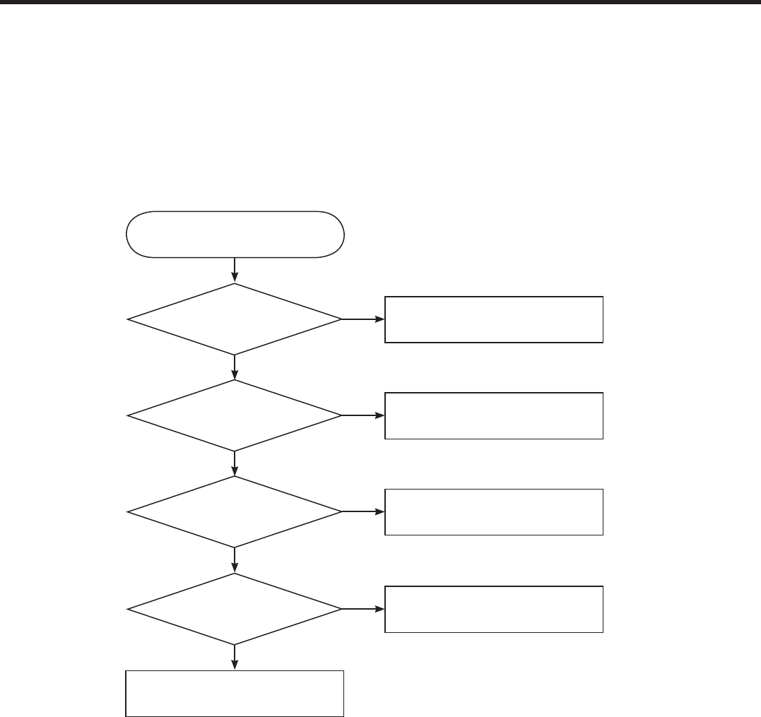
4.3 USB Troubleshooting
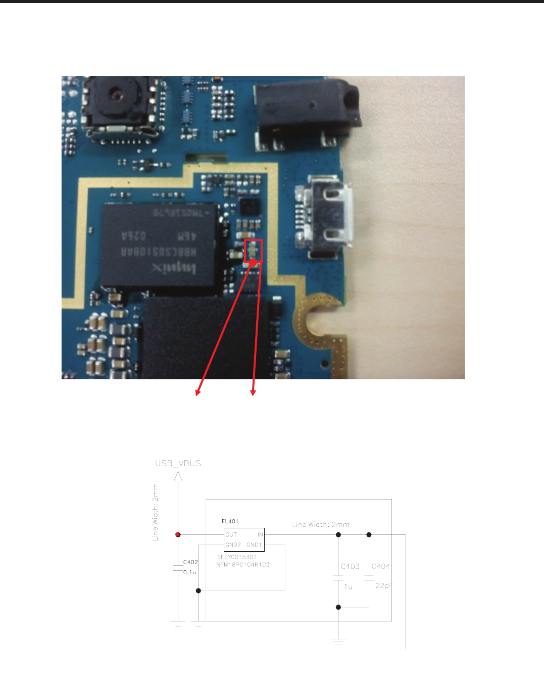
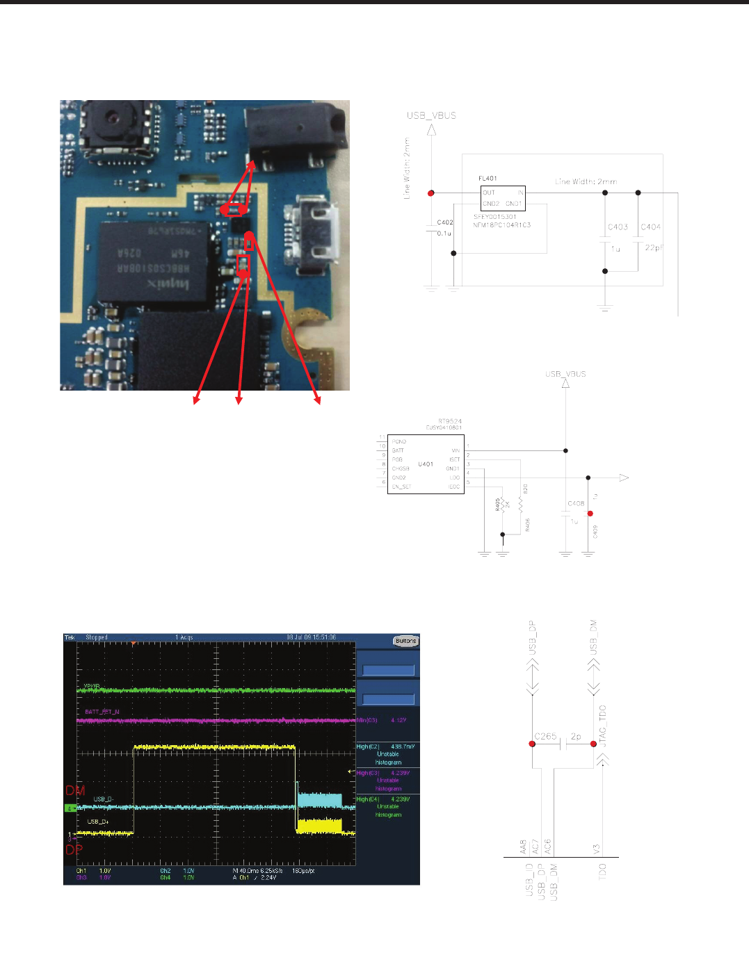
USB Initial sequence is : Isert USB Cable ÎUSB_VBUS +5V Check ÎIC400 triggered USB IF work
USB Troubleshooting
START
Cable is insert
physically? Change CN400
No
Yes
Change the main board
Is TP1_FL401(VBUS) voltage 5.1V? Change CN401
No
Yes
TP2_C409(LDO4.9V)
OUTPUT is about 5V? Change the U401
No
Yes
Is IC401 OUTPUT is TP3_C265(USB_
DM,USB_DP) signal OK? Change the IC401
No
Yes
[ USB Troubleshooting Flow ]
- 55 -
Copyright © 2010 LG Electronics. Inc. All right reserved.
Only for training and service purposes
LGE Internal Use Only
4. TROUBLE SHOOTING
USB Troubleshooting
kt
kw
TP1 TP2
TP3
FL401
VBUS_LDO_4V9
TP3 TP3
TP2
TP1
- 56 -
LGE Internal Use Only Copyright © 2010 LG Electronics. Inc. All right reserved.
Only for training and service purposes
4. TROUBLE SHOOTING
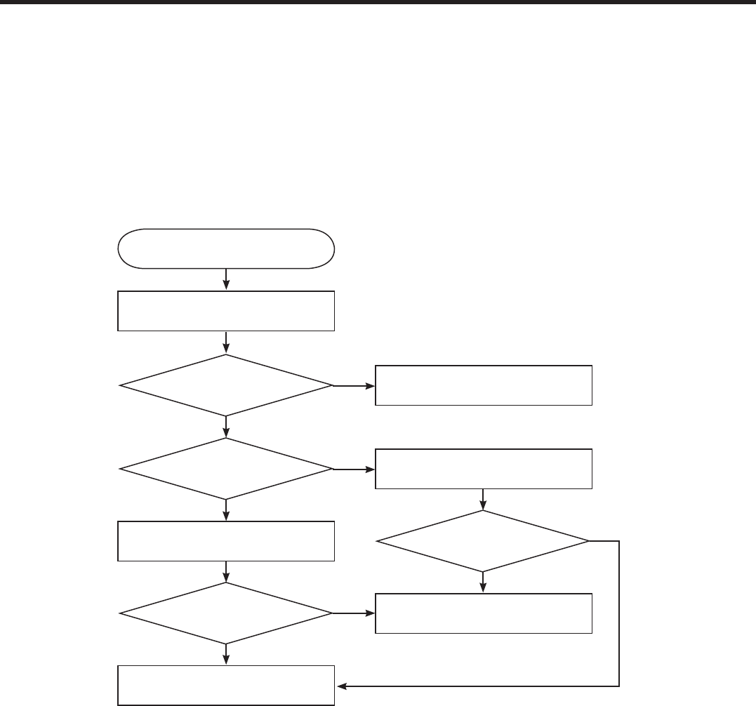
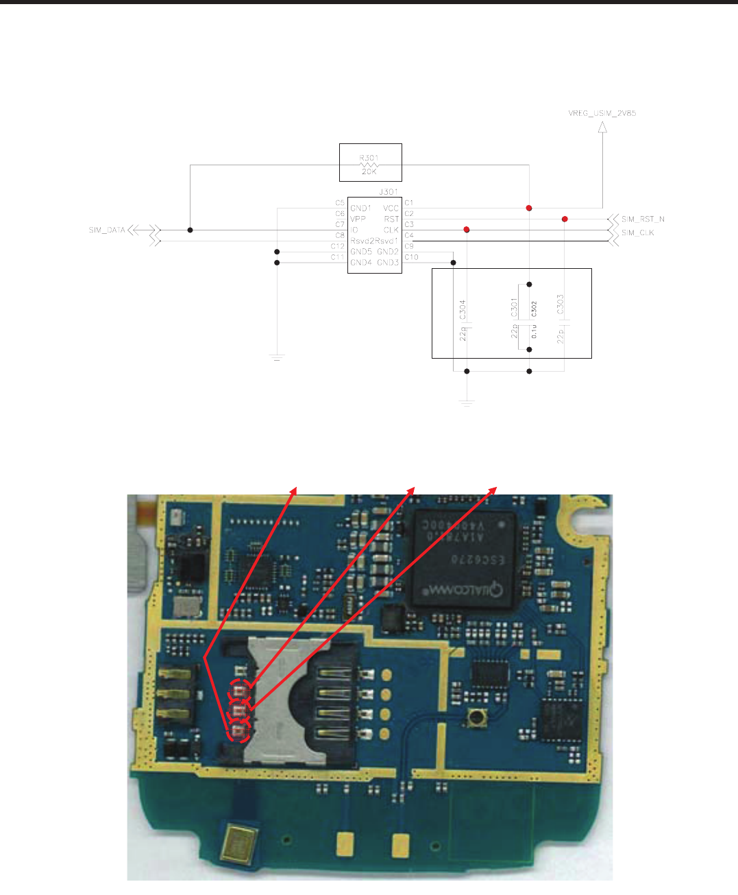
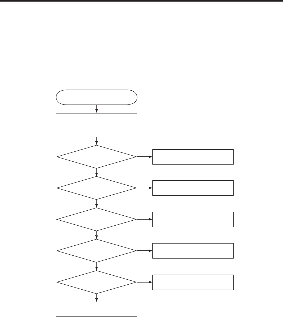
4.4 USIM Detect Troubleshooting
USIM Initial sequence is :
VREG_USIM_2.85V go to 1.8V or 3.0V ÆUSIM_CLK,USIM_RST,USIM_DATA triggered ÆUSIM IF work
USIM Troubleshooting
Re-insert the SIM card
Work well ?
No
END
END
Yes
Work well ? Change the Main board
START
Change the SIM card
Yes
No
TP1(Vreg_USIM) is 1.8V or 3.0V ?
TP2(USIM_CLK) & TP3(RST) is run ?
Yes
Check J301
No
No
Work well ? Yes
- 57 -
Copyright © 2010 LG Electronics. Inc. All right reserved.
Only for training and service purposes
LGE Internal Use Only
4. TROUBLE SHOOTING
USIM Troubleshooting
TP1 TP3TP2
MUSIM_DM MUSIM_DP
TP3
TP1
TP2
- 58 -
LGE Internal Use Only Copyright © 2010 LG Electronics. Inc. All right reserved.
Only for training and service purposes
4. TROUBLE SHOOTING
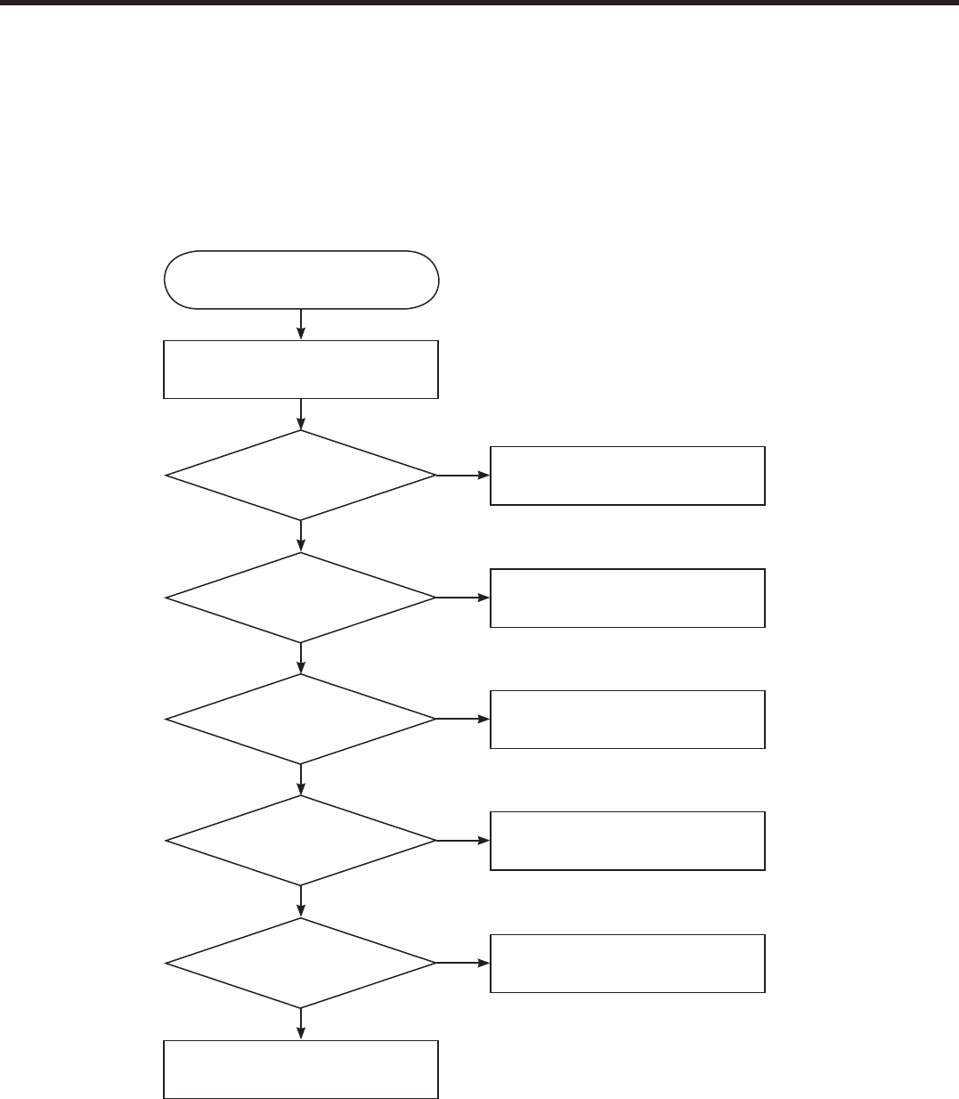
4.5 Camera Troubleshooting
Camera control signals are generated by QSC6270.
Camera Troubleshooting
START
CAM_AVDD_2.8V
CAM_VDD_1.8V (TP1, TP2) Chang the Main board
No
Yes
Change the Main board
Check the CAM_MCLK
TP4 Change the Main board
No
Check the CAM_PCLK
TP3 Change the Camera Module
No
Camera is OK END
Yes
No
Check the camera connection to the
socket and reconnect the camera
Camera is OK? END
Yes
No
- 59 -
Copyright © 2010 LG Electronics. Inc. All right reserved.
Only for training and service purposes
LGE Internal Use Only
4. TROUBLE SHOOTING
CAM_70MHz PCLK CAM_24MHz MCLK
Camera Troubleshooting
TP1 TP2
TP3
TP4
CAM_70MHz PCLK CAM_24MHz MCLK
Camera Troubleshooting
TP1 TP2
TP3
TP4
TP1
TP2
TP3
TP4
TP4TP3
- 60 -
LGE Internal Use Only Copyright © 2010 LG Electronics. Inc. All right reserved.
Only for training and service purposes
4. TROUBLE SHOOTING
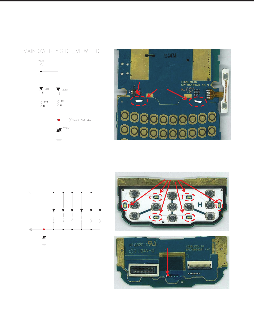
4.6 Main side view LED Troubleshooting
MAIN Key Pad LED is on as below :
Key pressing ÆLED_CON go down low (below 0.8v) ÆMAIN Key Backlight LED On
Main side view LED Troubleshooting
START
+VPWR is above 3.2V? Check battery
No
Yes
END
Change QSC6270
No
LED ON ? Change LED
No
Yes
Key press
When the LCD is on,
TP1 is below 0.8v
Yes
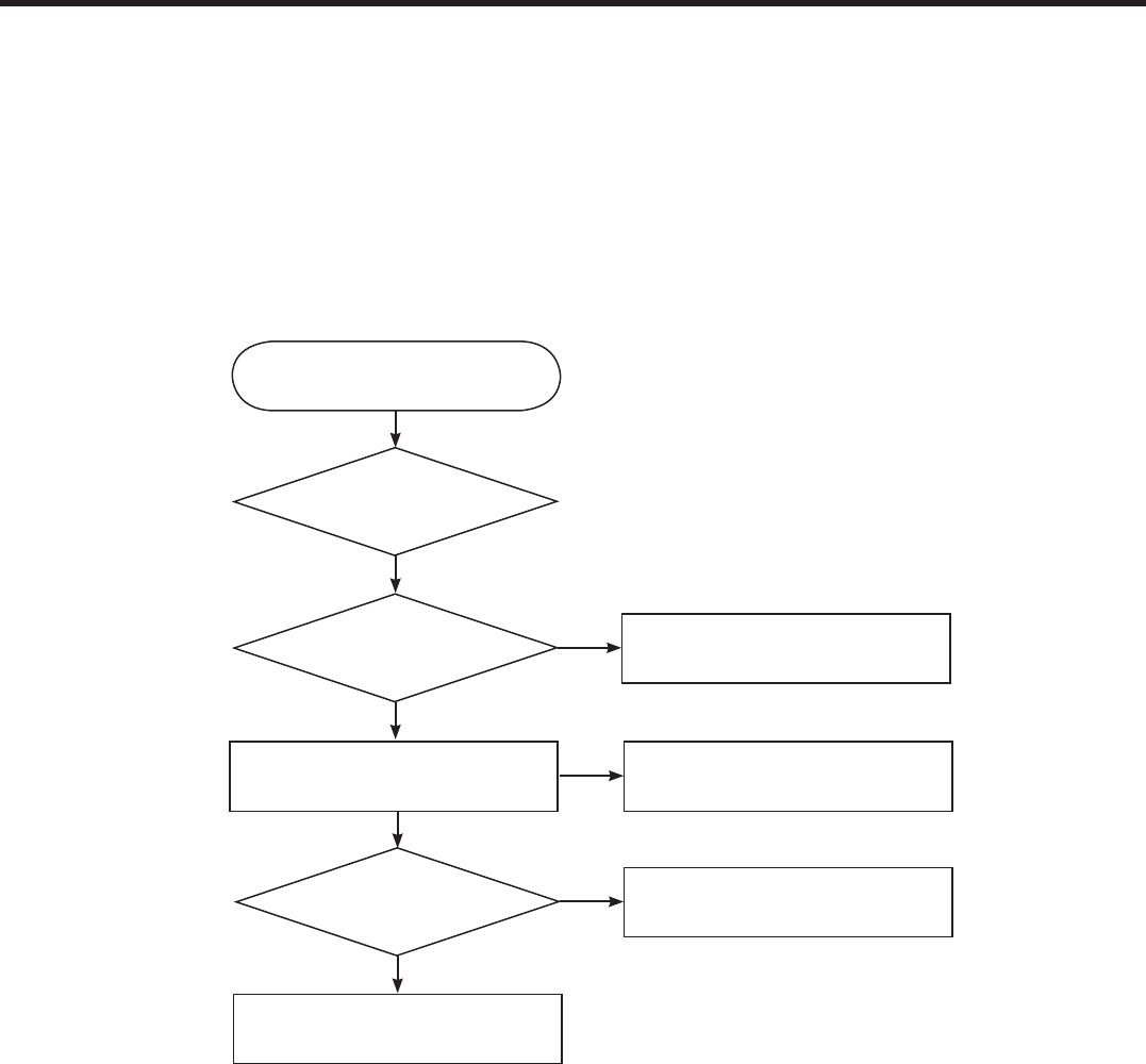
- 61 -
Copyright © 2010 LG Electronics. Inc. All right reserved.
Only for training and service purposes
LGE Internal Use Only
4. TROUBLE SHOOTING
4.7 Slide Key side view LED Troubleshooting
Sub Key Pad Slide is on as below :
Key pressing ÆLED_CON go down low (below 0.8v) ÆSub Key Backlight LED On
Slide Key side view LED Troubleshooting
START
+VPWR is above 3.2V? Check battery
No
Yes
END
Change the FPCB
or KEY PCB
No
LED ON ? Change the MAIN PCB
No
Yes
Key press
When the LCD is on,
TP2 is below 0.8v?
Yes
- 62 -
LGE Internal Use Only Copyright © 2010 LG Electronics. Inc. All right reserved.
Only for training and service purposes
4. TROUBLE SHOOTING
Slide Key side view Troubleshooting
LED
TP1
LED
TP2
TP1
LD103 LD104 LD105 LD108LD106 LD107
10
R107 R108
10 10
R105 R106
10 10
R109 R110
10
VA101
SLIDE_KEY_LED
WLED_VOUT
SUB KEY B/L
MAIN
SLIDE
TP2
- 63 -
Copyright © 2010 LG Electronics. Inc. All right reserved.
Only for training and service purposes
LGE Internal Use Only
4. TROUBLE SHOOTING
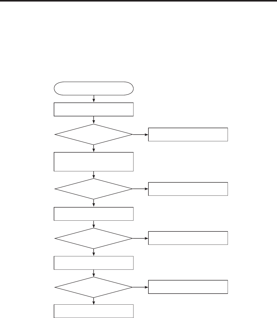
4.8 LCD Troubleshooting
LCD control signals are generated by QSC6270.
The signal path is : QSC6270 ÆCN102 ÆLCD Module
LCD Troubleshooting
Press END key
Key LED is on?
Yes
Change the Main Board
Move to KEY LED Troubleshooting
No
LCD display OK? END
START
Disconnect and reconnect
The LCD connector
(Slide PCB CN102,CN101)
LCD display OK?
Yes
Yes END
No
No
Change the FPCB
Change SUB PCB
LCD display OK? Yes END
No
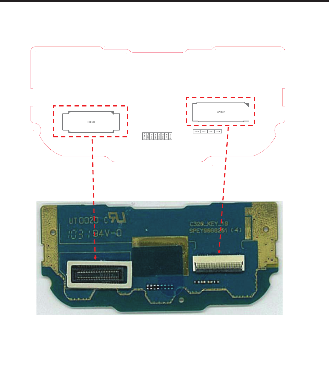
- 64 -
LGE Internal Use Only Copyright © 2010 LG Electronics. Inc. All right reserved.
Only for training and service purposes
4. TROUBLE SHOOTING
[Slide Side view placement]
LCD Troubleshooting
- 65 -
Copyright © 2010 LG Electronics. Inc. All right reserved.
Only for training and service purposes
LGE Internal Use Only
4. TROUBLE SHOOTING
4.9 Vibrator Troubleshooting
Vibrator is operate when DC motor driver is enabled.
Vibrator Troubleshooting
Operate the Vibrator
CN803(Main B/d)
and CN101(motor_FPCB) are well
connected ?
Yes
END
Reconnect Board to FPCB connector
No
Wired
Vibrator to FPCB
”VIB”?
Solder the wire on to FPCB
START
LINMOT_P
above 3.0V or LINMOT_M
below 1V?
No
Yes Change vibrator or
Change the Main PCB
No
Yes
Change the FPCB
working? No Change vibrator or
Change the Main PCB
Yes
- 66 -
LGE Internal Use Only Copyright © 2010 LG Electronics. Inc. All right reserved.
Only for training and service purposes
4. TROUBLE SHOOTING
F_SUB_FPCB to Main PCB Connector(CN101)
Main to F_SUB_FPCB Connector(CN803)
1
22
Motor Pad(CN101)
- 67 -
Copyright © 2010 LG Electronics. Inc. All right reserved.
Only for training and service purposes
LGE Internal Use Only
4. TROUBLE SHOOTING
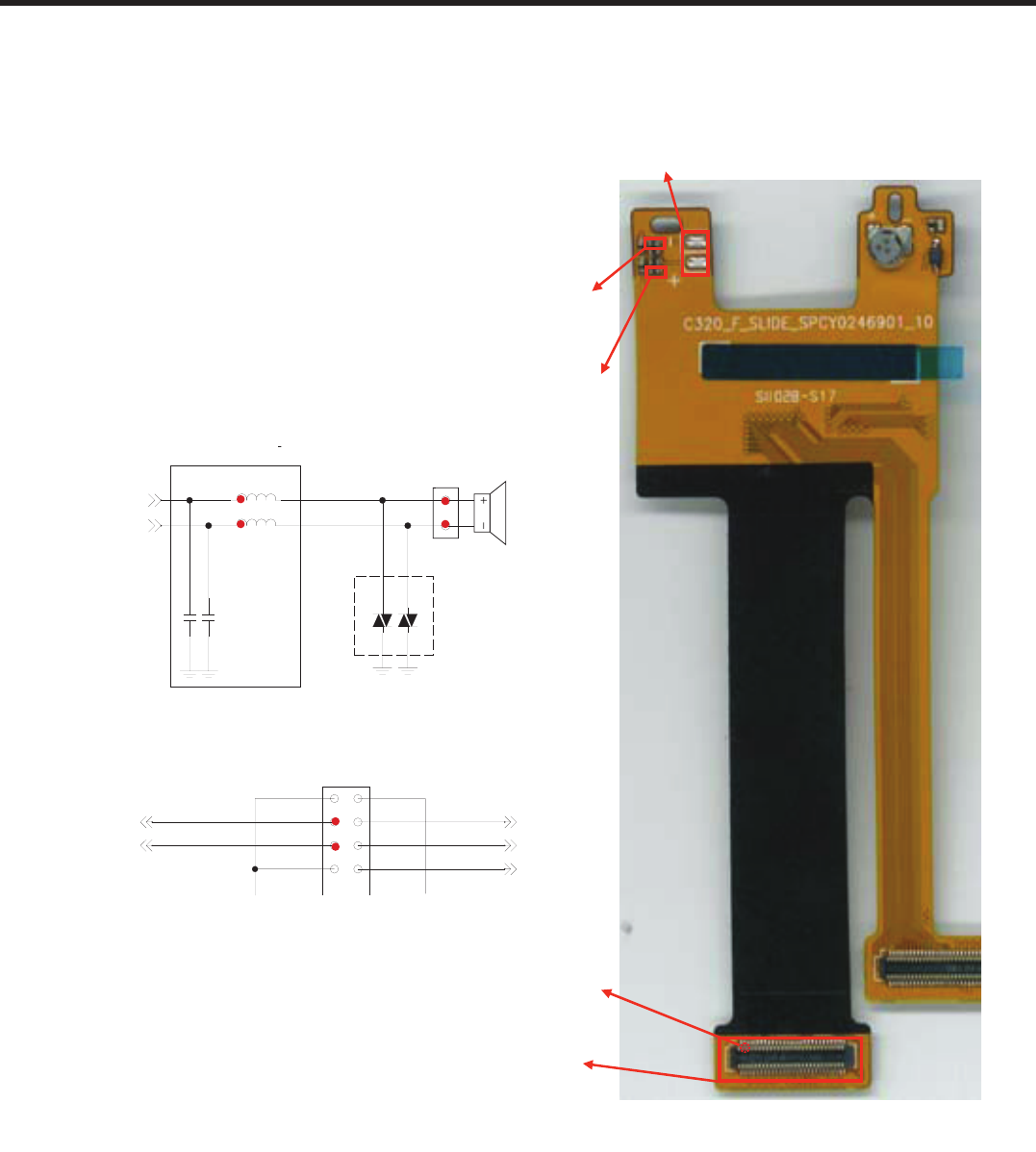
4.10 Receiver Path
QSC6270(3G disable) EAROP(EARON) ÆTP1_CN801(Main to Slide FPCB Connector) 2,3 PIN
ÆTP2_CN103(=Slide FPCB to Main PCB Connector) 2, 3 PIN ÆTP3_FB101, FB102(of F_SLIDE_ FPCB)
TP4_CN101(= Receiver Pad of F_SLIDE_ FPCB )
Connect the phone to network
Equipment and setup call
Setup 1KHz tone out
Can you hear the tone? END
Yes
No
Change the QSC6270
Change the Main PCB
The sine wave appears at
Receiver Pad(TP4)
Re-Solder Receiver
Change the Receiver
Yes
No
START
The sine wave appears at
TP3_FB101, FB102? Change F_SLIDE_FPCB
Yes
No
The sine wave appears at
TP2_CN103 2,3 PIN?
Re-Solder FB101,FB102
Change F_SLIDE_FPCB
Yes
No
The sine wave appears at
TP1_CN801 2,3 PIN?
Re-Connect CN103
Change F_SLIDE_FPCB
Yes
No
- 68 -
LGE Internal Use Only Copyright © 2010 LG Electronics. Inc. All right reserved.
Only for training and service purposes
4. TROUBLE SHOOTING
Main to Slide FPCB Connector(CN801)
1
27
TP1
15pF
15pF
15pF
VCOIN
RCV_P
RCV_N
LCD_DATA[4]
LCD_DATA[5]
LCD_DATA[6]
LCD_DATA[7]
LCD_VSYNC_OUT
LCD_RST_N
LCD_MAKER_ID
TP1
- 69 -
Copyright © 2010 LG Electronics. Inc. All right reserved.
Only for training and service purposes
LGE Internal Use Only
4. TROUBLE SHOOTING
TP4_Receiver PAD=CN101
127
Slide FPCB to Main PCB
Connector(CN103)
TP3_FB101
TP3_FB102
TP2
FB102 100n
10
1
AV
2
0
1C Fp
9
3
101C Fp93
CN101
2
1
2
0
1AV
FB101 100n
RCV_N
RCV_P
Can be Changed to TVS or ECLAMP
CN103
505
514
523
532
541
LCD_MAKER_IDRCV_N
RCV_P LCD_DATA[15]
LCD_DATA[14]
TP3
TP3
TP4
TP4
TP2
- 70 -
LGE Internal Use Only Copyright © 2010 LG Electronics. Inc. All right reserved.
Only for training and service purposes
4. TROUBLE SHOOTING
4.11 Headset path
QSC6270(3G disable) HPH_OUT_L_P/N ÆTP1_C506,C507 ÆIC501(Audio Sub System) Æ
TP2_R504,R505 ÆTP3_FB504, FB505 ÆJ501(=3.5pi Ear-jack)
Connect the phone to network
equipment and setup call.
Setup 1KHz tone out and insert headset.
Can you hear the tone? END
Yes
No
Change the Main board
Sine wave appears at
TP3_FB504, FB505
Re-solder or Change J501
Change the Main PCB
Yes
No
START
Sine wave appears at
TP2_R504, R505?
Re-solder the FB504, FB505
Change the Main PCB
Yes
No
Sine wave appears at
TP1_C506, C507? Change the IC501
Yes
No
- 71 -
Copyright © 2010 LG Electronics. Inc. All right reserved.
Only for training and service purposes
LGE Internal Use Only
4. TROUBLE SHOOTING
TP3_FB504
TP3_FB505
TP2_R504
TP2_R505
HS_GND
HS_MIC_P|Hook_ADC
FM_ANT
HS_OUT_R
HS_OUT_L
NC
TP2
TP2
TP3
TP3
- 72 -
LGE Internal Use Only Copyright © 2010 LG Electronics. Inc. All right reserved.
Only for training and service purposes
4. TROUBLE SHOOTING
Audio Sub system IC501TP1_C506TP1_C507
GND
HS_R
SPK_N
SPK_P
MUIC_AUD_FM_I2C_SCL
MUIC_AUD_FM_I2C_SDA
SPK_OUT_
N
SPK_OUT_P
HS_OUT_R
HS_OUT_L
HS_L
WM9093 is possible to 1.8 & 2.6 IO When HPVDD is 1.8V
TP1
TP1
- 73 -
Copyright © 2010 LG Electronics. Inc. All right reserved.
Only for training and service purposes
LGE Internal Use Only
4. TROUBLE SHOOTING
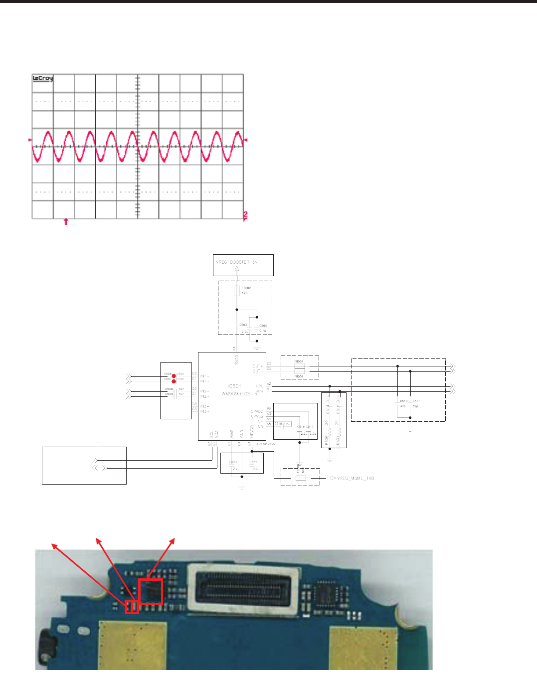
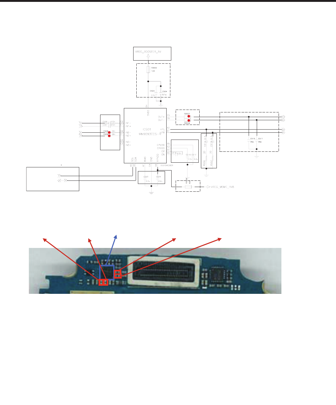
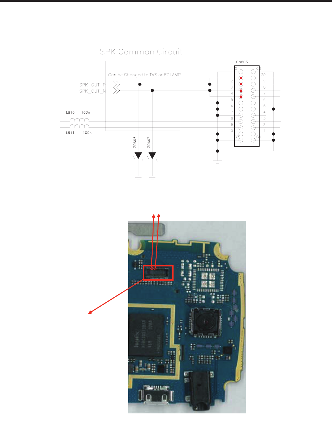
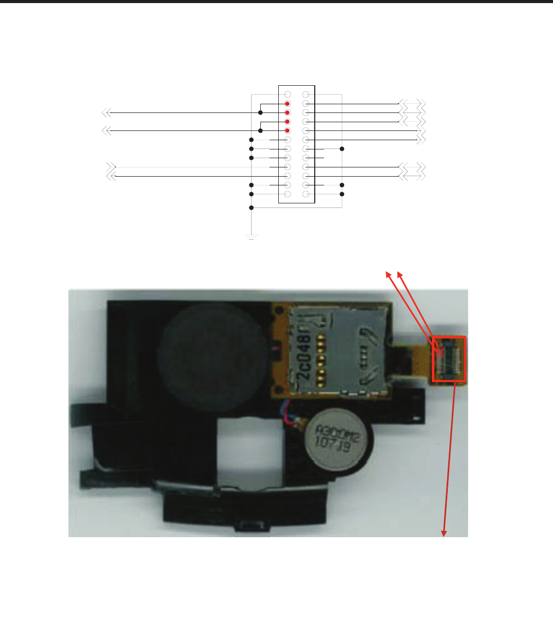
4.12 Speaker/Speaker Phone path
QSC6270 LINE_OUT_L_P/LINE_OUT_R_N ÆTP1_C508, C509ÆAudio Sub System(IC501) ÆTP2_FB507, FB508 Æ
TP3_CN803 1/2, 3/4 PIN(=Main to F_SUB_FPCB Connector) ÆTP4_CN101 1,2 PIN(=F_SUB_FPCB to Main PCB
Connector) ÆTP5_CN102(= Speaker Pad of F_SUB_FPCB)
Connect the phone to network
Equipment and setup call
Setup 1KHz tone out
Can you hear the tone? END
Yes
No
Change the QSC6270
Change the Main board
Sine wave appears at
TP5_Speaker Pad
Re-Solder Speaker Pad
Change the Speaker
Yes
No
START
Sine wave appears at
TP4_CN101 1,2 PIN Change the F_SUB FPCB
Yes
No
Sine wave appears at
TP3_CN803 1/2, 3/4 PIN
Re-Connect the CN101
Change the F_SUB FPCB
Yes
No
Sine wave appears at
TP2_FB507, FB508 Change the Main PCB
Yes
No
Sine wave appears at
TP1_C508, C509 Change the IC501
Yes
No
- 74 -
LGE Internal Use Only Copyright © 2010 LG Electronics. Inc. All right reserved.
Only for training and service purposes
4. TROUBLE SHOOTING
TP1_C508
Audio Sub
System(IC501)
TP1_C509 TP2_FB507 TP2_FB508
GND
HS_R
SPK_N
SPK_P
MUIC_AUD_FM_I2C_SCL
MUIC_AUD_FM_I2C_SDA
SPK_OUT_
N
SPK_OUT_P
HS_OUT_R
HS_OUT_L
HS_L
WM9093 is possible to 1.8 & 2.6 IO When HPVDD is 1.8V
TP1
TP1
TP2
TP2
- 75 -
Copyright © 2010 LG Electronics. Inc. All right reserved.
Only for training and service purposes
LGE Internal Use Only
4. TROUBLE SHOOTING
TP3
Main to F_SUB_FPCB
Connector(CN803)
110
TP3
TP3
- 76 -
LGE Internal Use Only Copyright © 2010 LG Electronics. Inc. All right reserved.
Only for training and service purposes
4. TROUBLE SHOOTING
F_SUB_FPCB to Main PCB
Connector(CN101)
1
10
TP4
CN101
1110
129
138
147
156
165
174
183
192
201
G1 G2
G3 G4
MOTOR_POWER_N
SPK_OUT_P
SPK_OUT_N
MSD_D[3]
MSD_D[2]
MSD_D[1]
MSD_CMD
VBAT
MSD_D[0]
MSD_CLK
VREG_MICROSD_3V0
TP4
- 77 -
Copyright © 2010 LG Electronics. Inc. All right reserved.
Only for training and service purposes
LGE Internal Use Only
4. TROUBLE SHOOTING
TP5_CN102(=Speaker Pad)
2
1
CN102
SPK_OUT_P
SPK_OUT_N
Can be Changed to TVS or ECLAMP
TP5
- 78 -
LGE Internal Use Only Copyright © 2010 LG Electronics. Inc. All right reserved.
Only for training and service purposes
4. TROUBLE SHOOTING
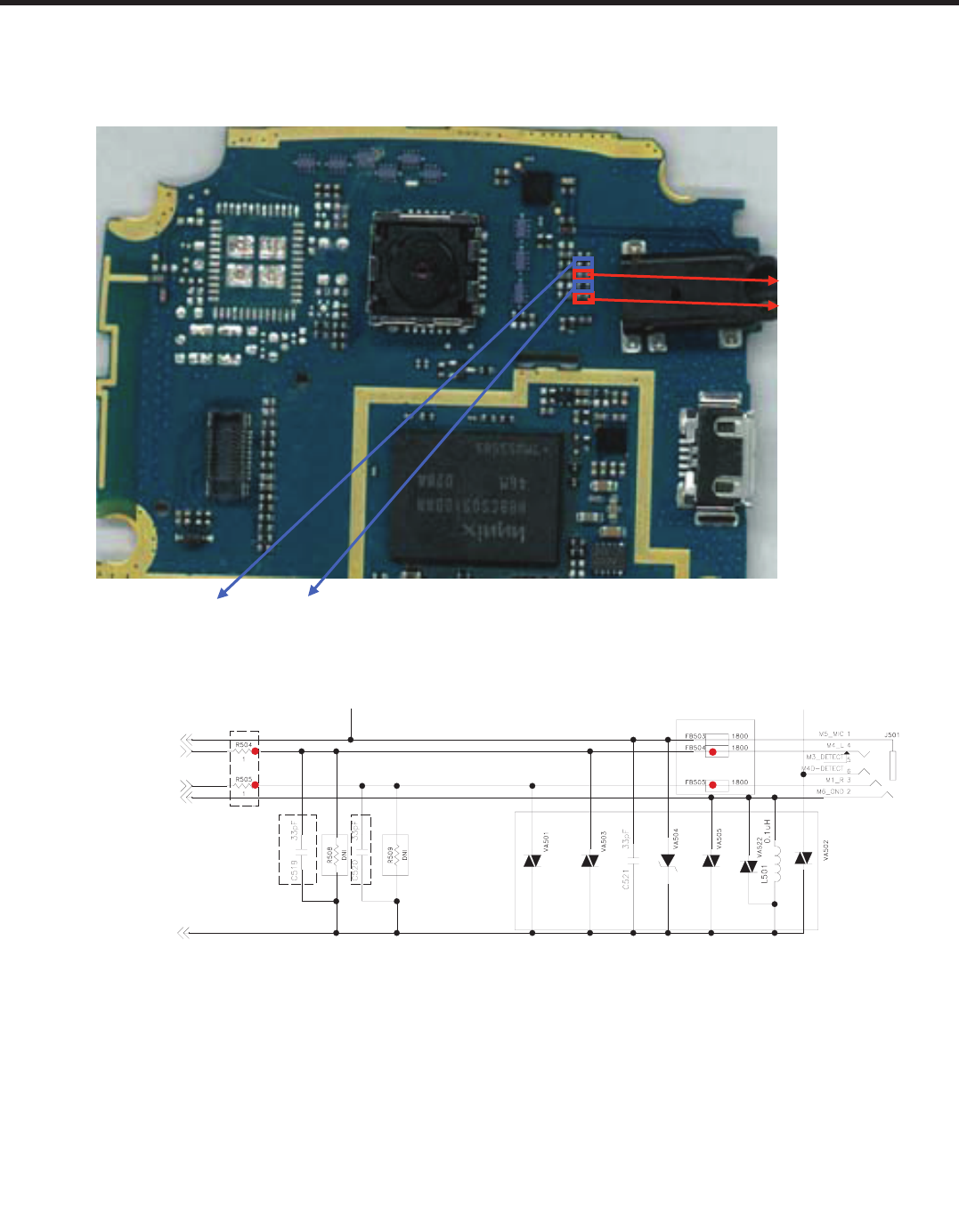
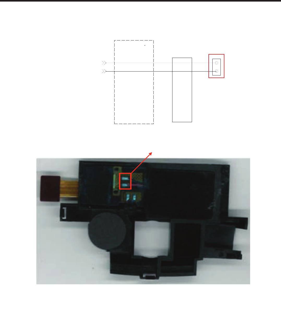
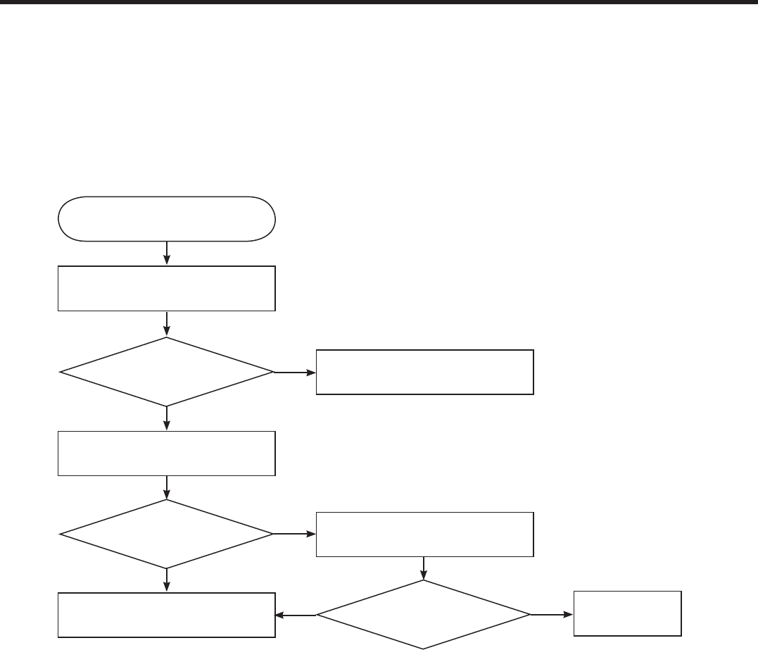
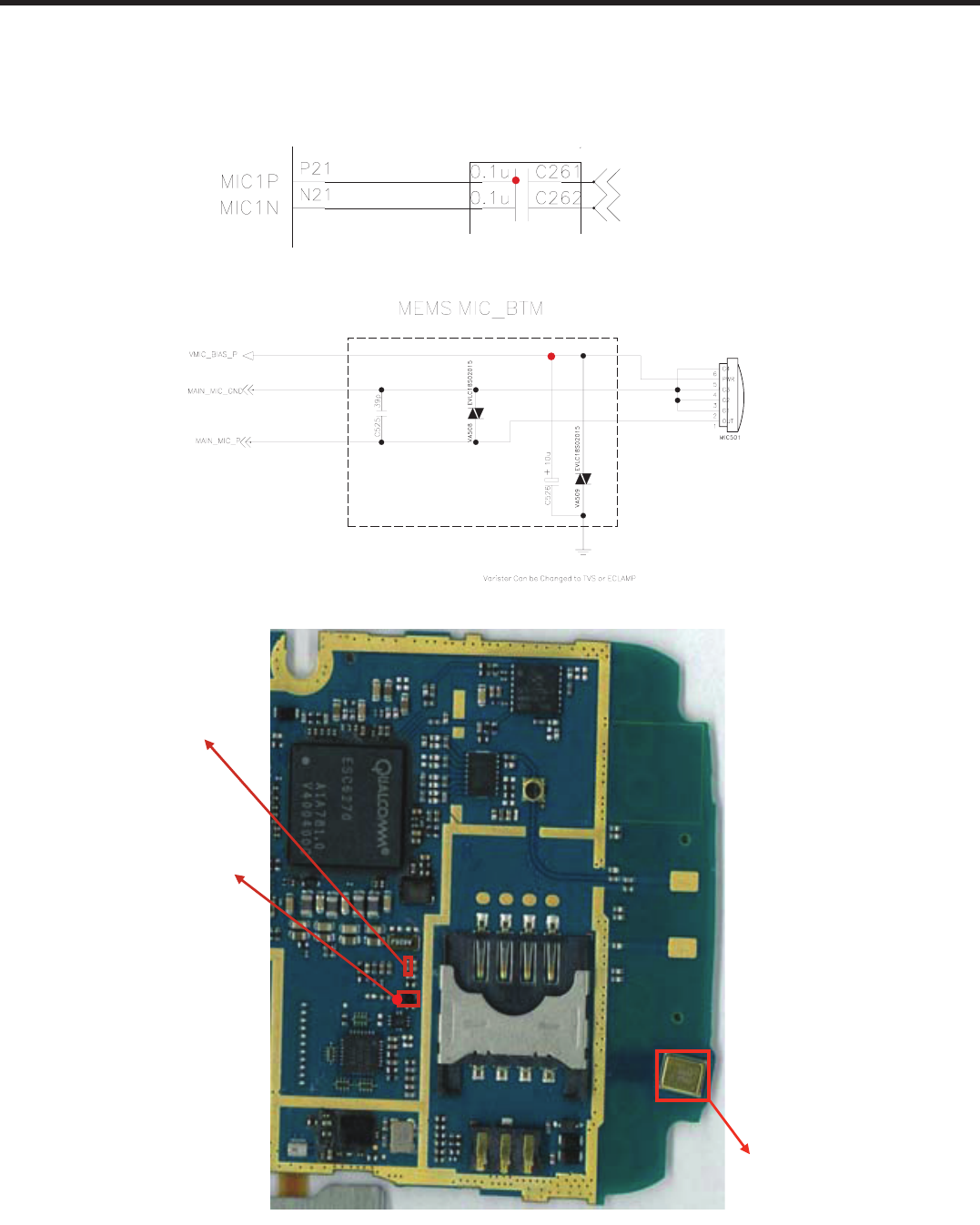
4.13 Main microphone
MIC501 ÆVMIC_BIAS_P(TP1_C526) ÆMAIN_MIC_P(TP2_C261) ÆMIC1P PAD of QSC6270(3G disable)
Make a call
MIC_BIAS(TP1_C526)
is about 1.8V?
Yes
Change the Main board
No
Sine wave appears at
TP2_C261? Change the MIC
START
Make sound to MIC
Yes
No
Change the Main board Work well? Yes END
No
- 79 -
Copyright © 2010 LG Electronics. Inc. All right reserved.
Only for training and service purposes
LGE Internal Use Only
4. TROUBLE SHOOTING
MIC501
TP1_C526
TP2_C261
DNG_CIM
_
N
IA
M
P
_C
I
M_
N
IA
M
TP2
TP1
- 80 -
LGE Internal Use Only Copyright © 2010 LG Electronics. Inc. All right reserved.
Only for training and service purposes
4. TROUBLE SHOOTING
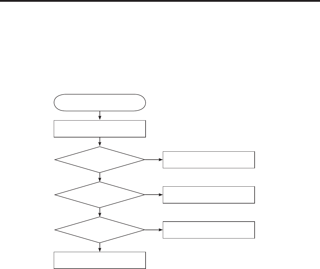
4.14 Headset microphone
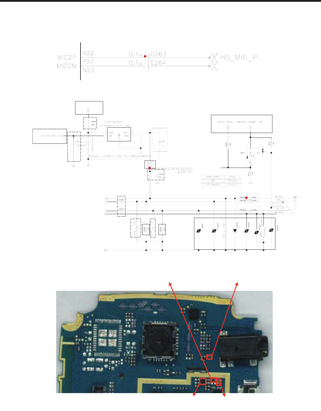
3.5 pie Headset ÆHS_MIC_BIAS(TP1_R502) ÆHS_MIC_P(TP2_FB503) ÆHS_MIC_P(TP3_C263)
ÆMIC2P PAD of QSC6270(3G disable)
Insert Headset & Make a call
TP1_R502 is About 1.8V ? Change the LDO(U501)
Change the Main board
No
Yes
Change the Headset
Change the MAIN board
Sine wave appears at
TP2_FB503?
Re-Solder FB503
Change the MAIN board
No
Yes
Sine wave appears at
TP3_C263?
Re-Solder C263
Change the MAIN board
START
Yes
No
- 81 -
Copyright © 2010 LG Electronics. Inc. All right reserved.
Only for training and service purposes
LGE Internal Use Only
4. TROUBLE SHOOTING
TP1_R502 TP2_FB503
TP3_C263U501
DNG
_
S
H
TP3
VREG_MSMP_2V6
HS_GND
HS_MIC_P|Hook_ADC
FM_ANT
HS_OUT_R
HS_OUT_L
HS_JACK_DET
´ëüǰ : EUSY0407501
NC
RP183K181D is possible to 1.8 & 2.6 IO
TP1
TP2
- 82 -
LGE Internal Use Only Copyright © 2010 LG Electronics. Inc. All right reserved.
Only for training and service purposes
4. TROUBLE SHOOTING
㝘⪌HG 㵬㦤G 㠄⸬㡸G 㵲㡸G ㍌G 㛺㏩⏼␘UU㝘⪌HG 㵬㦤G 㠄⸬
㡸G 㵲㡸G ㍌G 㛺㏩⏼␘UG
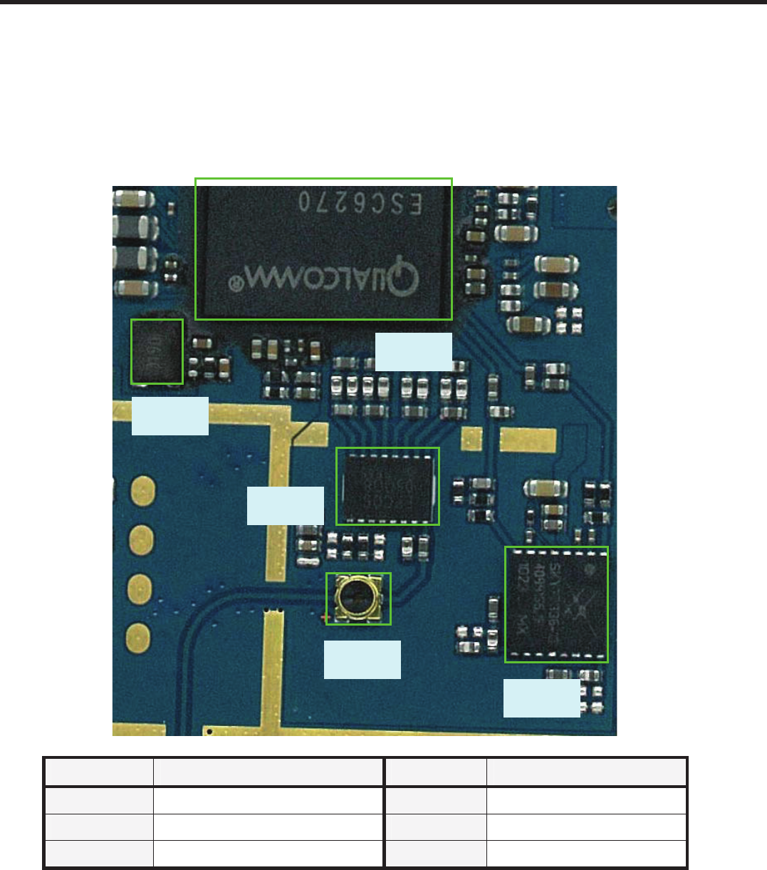
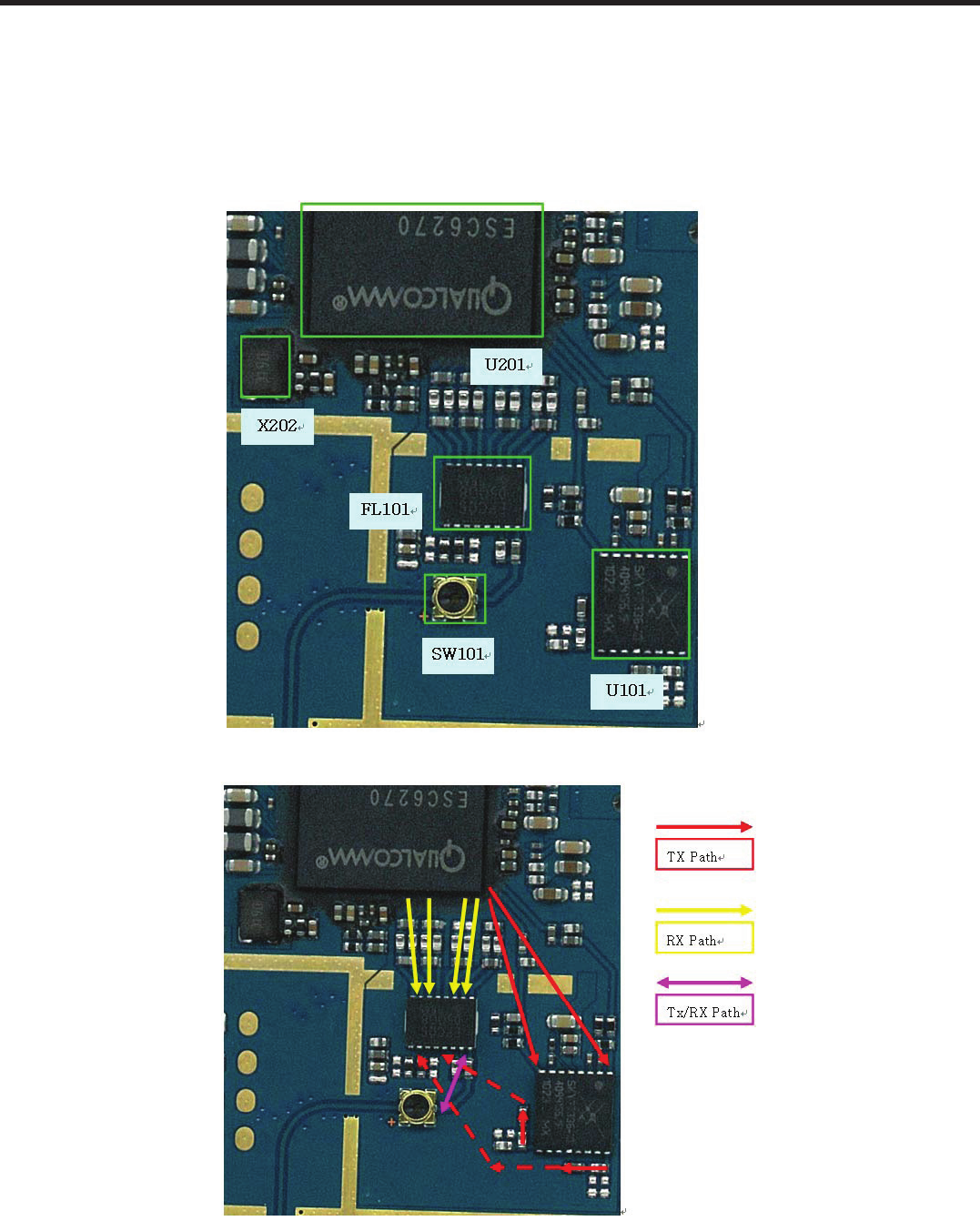
4.15 RF Component
MAIN board Bottom
RF component (GSM)
Reference Description Reference Description
U201 QSC6270 3G disable FL101 FEM
X202 XO SW101 RF connector
U101 GSM(EDGE) TX PAM
FL101
SW101
U101
X202
U201
4.15 RF Component
- 83 -
Copyright © 2010 LG Electronics. Inc. All right reserved.
Only for training and service purposes
LGE Internal Use Only
4. TROUBLE SHOOTING
㝘⪌HG 㵬㦤G 㠄⸬㡸G 㵲㡸G ㍌G 㛺㏩⏼␘UU㝘⪌HG 㵬㦤G 㠄⸬
㡸G 㵲㡸G ㍌G 㛺㏩⏼␘UG G
G
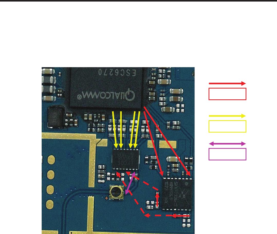
4.16 RF Path
4.16.1 GSM path
T
X Path
RX Path
T
x/RX Path
4.16 RF Path
- 84 -
LGE Internal Use Only Copyright © 2010 LG Electronics. Inc. All right reserved.
Only for training and service purposes
4. TROUBLE SHOOTING
㝘⪌HG 㵬㦤G 㠄⸬㡸G 㵲㡸G ㍌G 㛺㏩⏼␘UU㝘⪌HG 㵬㦤G 㠄⸬
㡸G 㵲㡸G ㍌G 㛺㏩⏼␘UG G
G
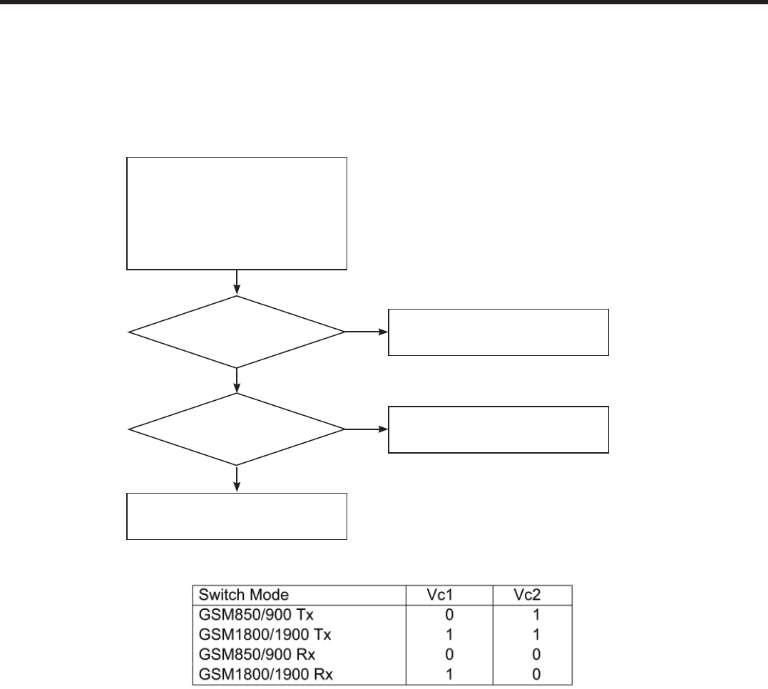
4.17 Trouble Shooting of GSM Part
(GSM850/GSM900/1800/1900)
㝘⪌HG 㵬㦤G 㠄⸬㡸G 㵲㡸G ㍌G 㛺㏩⏼␘UU㝘⪌HG 㵬㦤G 㠄⸬
㡸G 㵲㡸G ㍌G 㛺㏩⏼␘UG G
G
=
- 85 -
Copyright © 2010 LG Electronics. Inc. All right reserved.
Only for training and service purposes
LGE Internal Use Only
4. TROUBLE SHOOTING
Setup Test Equipnment
Cell power = -74dbm
EGSM CH: 38
DCS1800 CH: 698
PCS1900 CH: 661
GSM850 CH: 190
Check M/S & FEM
(SW101 & FL101)
Check
Rx Part
Check
Tx Part
START
END
- 86 -
LGE Internal Use Only Copyright © 2010 LG Electronics. Inc. All right reserved.
Only for training and service purposes
4. TROUBLE SHOOTING
㝘⪌HG 㵬㦤G 㠄⸬㡸G 㵲㡸G ㍌G 㛺㏩⏼␘UU㝘⪌HG 㵬㦤G 㠄⸬
㡸G 㵲㡸G ㍌G 㛺㏩⏼␘UG G
G
4.17.1 Checking Front-End Module Block
Setup Test Equipnment
Cell power = -74dbm
EGSM CH: 38
DCS1800 CH: 698
PCS1900 CH: 661
GSM850 CH: 190
Check TP3=2.85V? Check U201
No
Yes
END
Check the logic in each
Mood TP1~TP2 high level
2.85V ≥ Vcc ≥ L4V?
Replace FL101
No
Yes
4.17.1 Checking Front-End Module Block
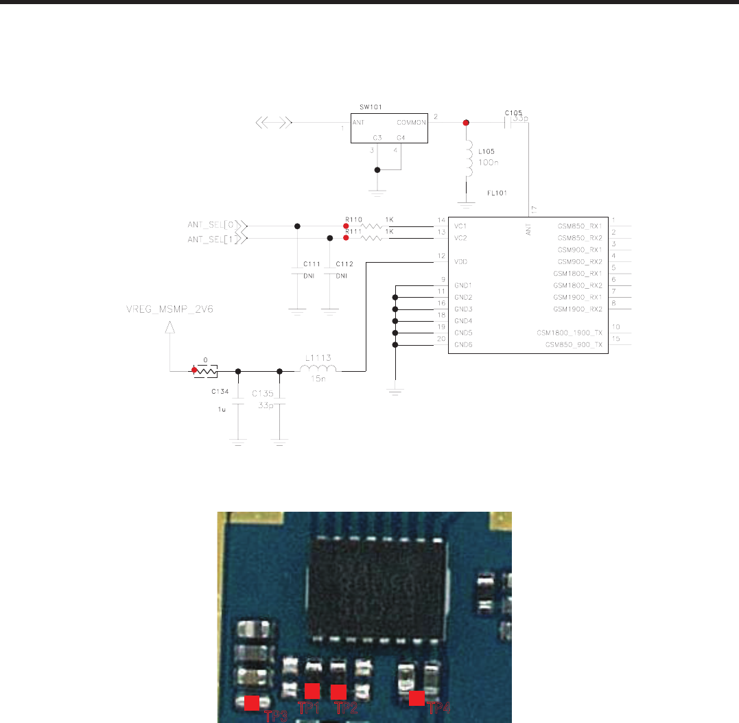
- 87 -
Copyright © 2010 LG Electronics. Inc. All right reserved.
Only for training and service purposes
LGE Internal Use Only
4. TROUBLE SHOOTING
㝘⪌HG 㵬㦤G 㠄⸬㡸G 㵲㡸G ㍌G 㛺㏩⏼␘UU㝘⪌HG 㵬㦤G 㠄⸬
㡸G 㵲㡸G ㍌G 㛺㏩⏼␘UG G
G
51
51
51
51
51 51 51
51
850, 900,1800,1900MHz
R109
ANT_FEED
TP4
TP1
TP2
TP3
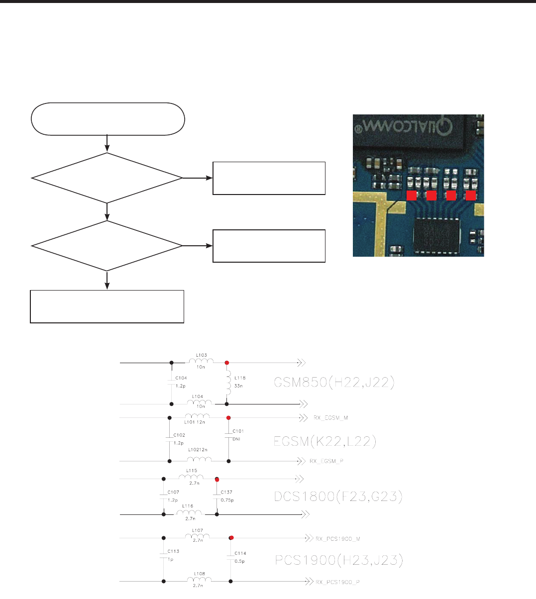
- 88 -
LGE Internal Use Only Copyright © 2010 LG Electronics. Inc. All right reserved.
Only for training and service purposes
4. TROUBLE SHOOTING
㝘⪌HG 㵬㦤G 㠄⸬㡸G 㵲㡸G ㍌G 㛺㏩⏼␘UU㝘⪌HG 㵬㦤G 㠄⸬
㡸G 㵲㡸G ㍌G 㛺㏩⏼␘UG G
G
51 51 51 51
RX_DCS1800_M
RX_DCS1800_P
RX_GSM850_M
RX_GSM850_P
TP1
TP2
TP3
TP4
4.17.2 Checking GSM Rx part
Check TP1~TP3
Signal exist?
No
Yes
Re-download & calibration
Rx still has problem?
Check FEM & Soldeing of TPs
GSM Rx is OK
No
Yes
START
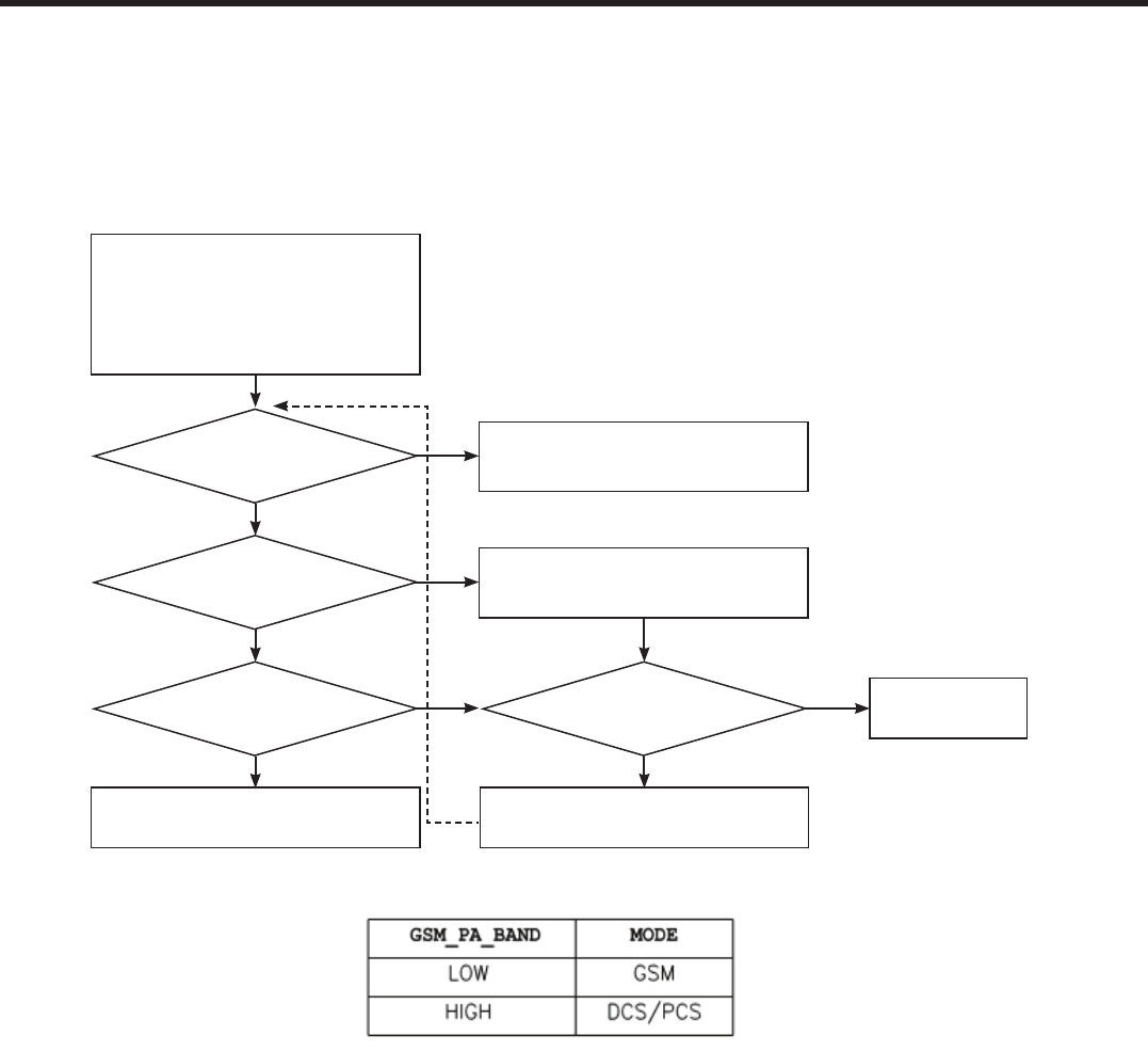
- 89 -
Copyright © 2010 LG Electronics. Inc. All right reserved.
Only for training and service purposes
LGE Internal Use Only
4. TROUBLE SHOOTING
㝘⪌HG 㵬㦤G 㠄⸬㡸G 㵲㡸G ㍌G 㛺㏩⏼␘UU㝘⪌HG 㵬㦤G 㠄⸬
㡸G 㵲㡸G ㍌G 㛺㏩⏼␘UG G
G
4.17.3 Checking GSM Tx part
Table 4.17.3 GPAM Logic Control
Setup Test Equipnment
Cell power = -60dbm
Tx Power Level Set
GSM850/GSM900 = 5,
DCS/PCS = 0
Is the level of TP4 same
to Table 4.17.3
TP2, 30dBm over?
TP3, 33dBm over?
Check TP1,
GSM850, EGSM 32dBm
DCS,PCS 29dBm over?
Re-download & calibration
Yes
Check U201
No
Remove U101 and check
The power of pin1, pin8 (on board)
No
The power of pin1, pin8
Replace U101
No
Check U201
No
Yes
Yes
Yes
Yes
Yes
4.17.3 Checking GSM Tx part
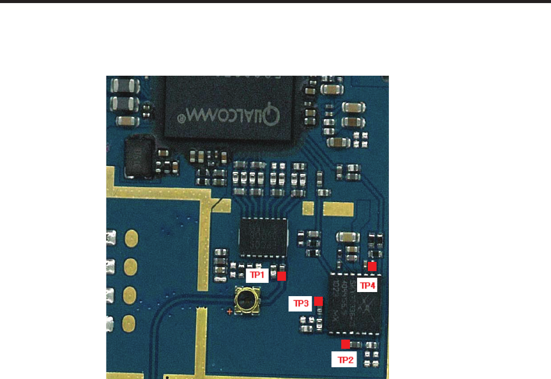
- 90 -
LGE Internal Use Only Copyright © 2010 LG Electronics. Inc. All right reserved.
Only for training and service purposes
4. TROUBLE SHOOTING
㝘⪌HG 㵬㦤G 㠄⸬㡸G 㵲㡸G ㍌G 㛺㏩⏼␘UU㝘⪌HG 㵬㦤G 㠄⸬
㡸G 㵲㡸G ㍌G 㛺㏩⏼␘UG G
G
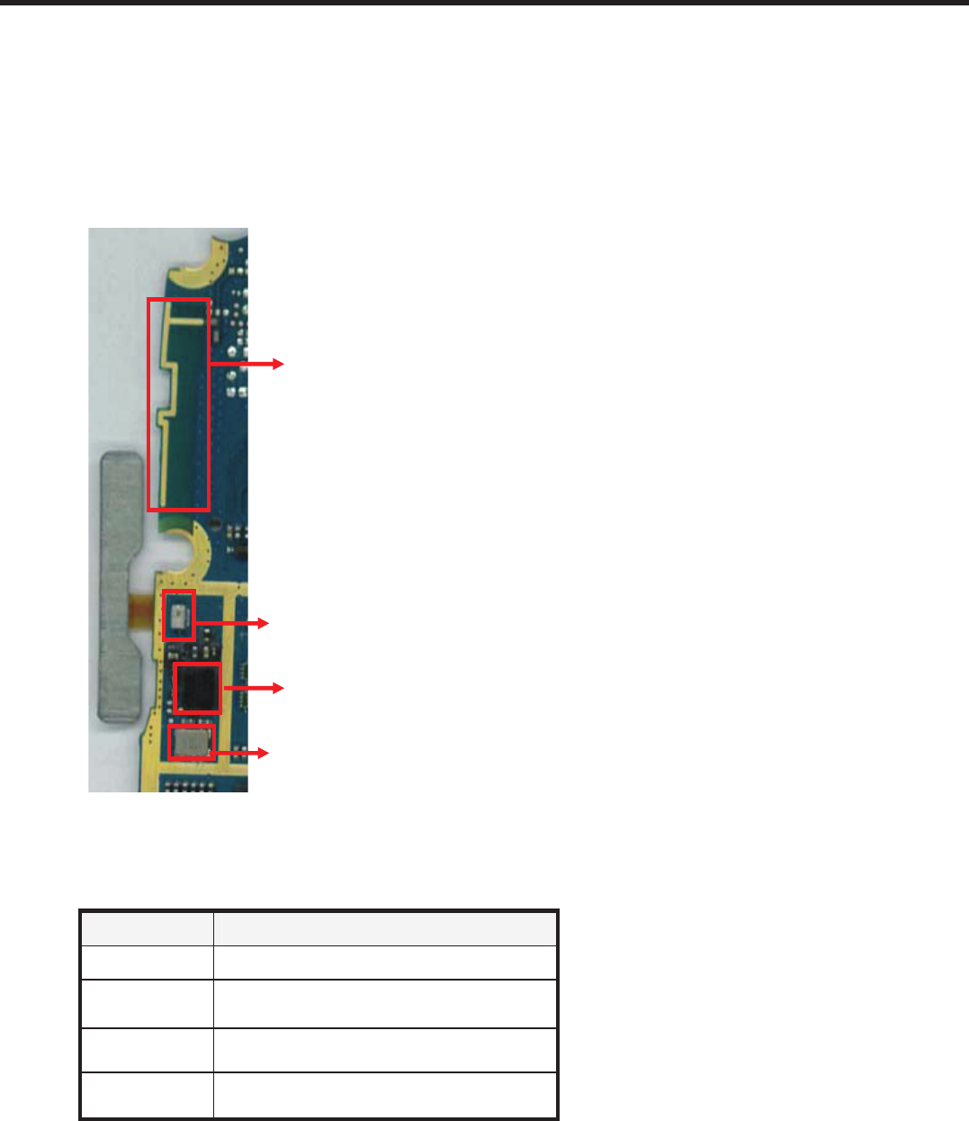
- 91 -
Copyright © 2010 LG Electronics. Inc. All right reserved.
Only for training and service purposes
LGE Internal Use Only
4. TROUBLE SHOOTING
㝘⪌HG 㵬㦤G 㠄⸬㡸G 㵲㡸G ㍌G 㛺㏩⏼␘UU㝘⪌HG 㵬㦤G 㠄⸬
㡸G 㵲㡸G ㍌G 㛺㏩⏼␘UG G
G
4.18 Checking Bluetooth Block
4.18.1 BLUETOOTH RF components
RF component ( BT )
- Main board bottom -
Reference Description
ANT BT Pattern ANT
U703 BT module_BCM2070
FL701 Band pass filter
X702 26Mhz crystal
U703
X702
FL701
ANT
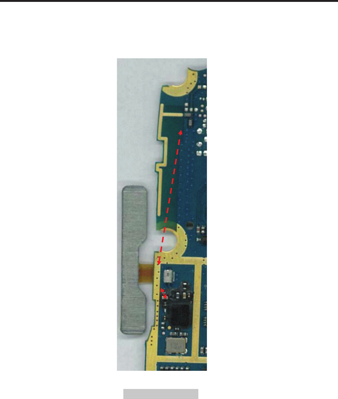
- 92 -
LGE Internal Use Only Copyright © 2010 LG Electronics. Inc. All right reserved.
Only for training and service purposes
4. TROUBLE SHOOTING
㝘⪌HG 㵬㦤G 㠄⸬㡸G 㵲㡸G ㍌G 㛺㏩⏼␘UU㝘⪌HG 㵬㦤G 㠄⸬
㡸G 㵲㡸G ㍌G 㛺㏩⏼␘UG G
G
4.18.2 BLUETOOTH SIGNAL PATH
Bluetooth Signal PATH (Main board bottom)
Bluetooth T/Rx PATH
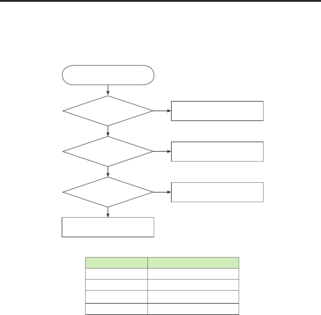
- 93 -
Copyright © 2010 LG Electronics. Inc. All right reserved.
Only for training and service purposes
LGE Internal Use Only
4. TROUBLE SHOOTING
㝘⪌HG 㵬㦤G 㠄⸬㡸G 㵲㡸G ㍌G 㛺㏩⏼␘UU㝘⪌HG 㵬㦤G 㠄⸬
㡸G 㵲㡸G ㍌G 㛺㏩⏼␘UG G
G
4.18.3 BLUETOOTH Trouble shooting
TP# TP description
TP1 VREG_MSMP_2.6V
TP2 VREG_MSME_1.8V
TP3 BT_CLK(26Mhz)
TP4 BT_ANT_OUT
START
Check TP1, TP2
Signal exist? Change the main board
No
Yes
Change the main board
Check TP3
IS clock OK? Check X700
No
Yes
Check TP4
Signal exist? Check U700
No
Yes
4.18.3 BLUETOOTH Trouble shooting
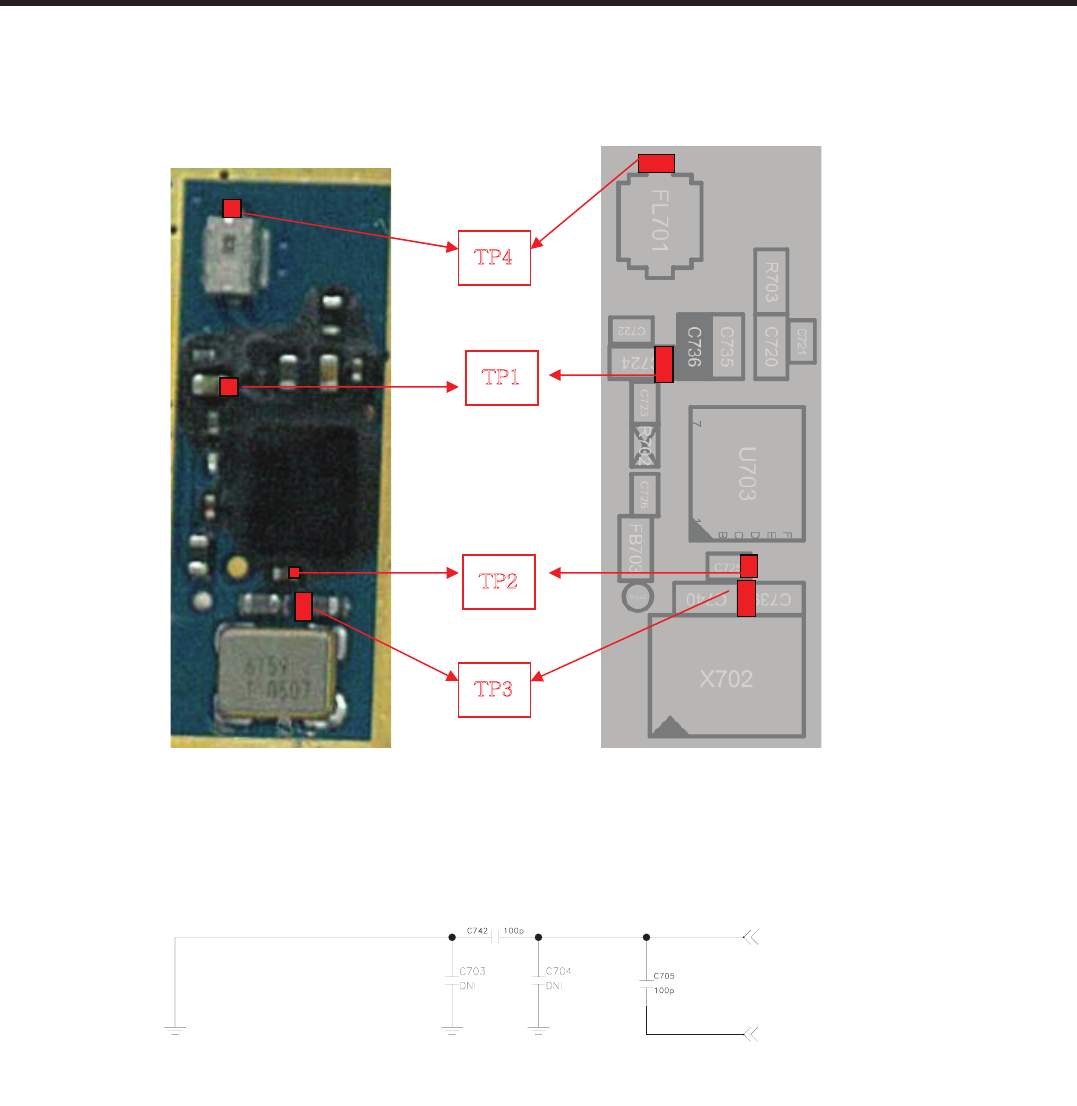
- 94 -
LGE Internal Use Only Copyright © 2010 LG Electronics. Inc. All right reserved.
Only for training and service purposes
4. TROUBLE SHOOTING
㝘⪌HG 㵬㦤G 㠄⸬㡸G 㵲㡸G ㍌G 㛺㏩⏼␘UU㝘⪌HG 㵬㦤G 㠄⸬
㡸G 㵲㡸G ㍌G 㛺㏩⏼␘UG G
G
{wX
{wYG
{wZG
{w[G
WLAN_BT_ANT_FEED
BT_ANT_FEED
Connectivity_ANT_PAD
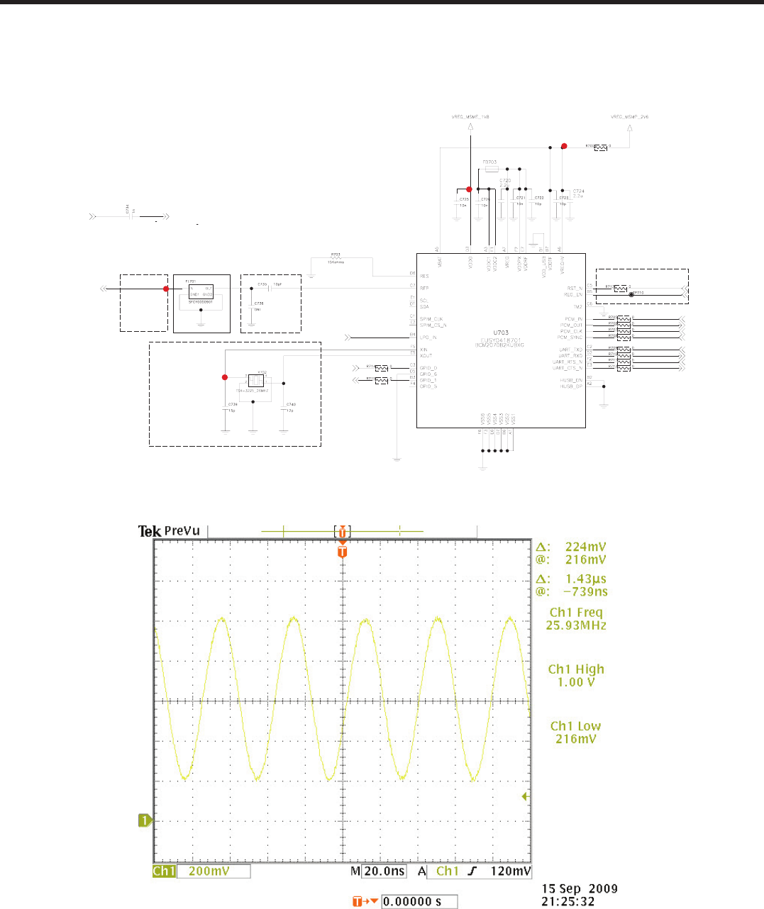
- 95 -
Copyright © 2010 LG Electronics. Inc. All right reserved.
Only for training and service purposes
LGE Internal Use Only
4. TROUBLE SHOOTING
㝘⪌HG 㵬㦤G 㠄⸬㡸G 㵲㡸G ㍌G 㛺㏩⏼␘UU㝘⪌HG 㵬㦤G 㠄⸬
㡸G 㵲㡸G ㍌G 㛺㏩⏼␘UG G
G
[BT main clk : 26MHz]
{wX
{wY
{wZ
{w[G
26MHz
A4
C4
E4
D4
RTC_32K
BT_WAKEUP
BT_PCM_CLK
BT_PCM_OUT
BT_PCM_IN
BT_PCM_SYNC
BT_UART_RTS
BT_UART_CTS
BT_WAKEUP_HOST
BT_RST_N
BT_ANT_FEED
RTC_32K768
RTC_32K768
BT_UART_RX
BT_UART_TX
BT_PWR_ON
must have 1% tolerance
can be removed
When power class 1.5 is used, R307 is populated and R308 is depopulated.
(Vice versa for power class 2)
Class 1.5
TP1
TP3
TP4
TP2
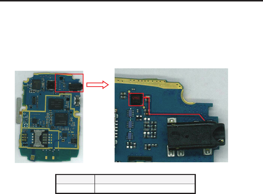
- 96 -
LGE Internal Use Only Copyright © 2010 LG Electronics. Inc. All right reserved.
Only for training and service purposes
4. TROUBLE SHOOTING
㝘⪌HG 㵬㦤G 㠄⸬㡸G 㵲㡸G ㍌G 㛺㏩⏼␘UU㝘⪌HG 㵬㦤G 㠄⸬
㡸G 㵲㡸G ㍌G 㛺㏩⏼␘UG G
G
4.19 Checking FM Radio Block
4.19.1 FM Signal Path
Reference Description
U701 TEA5991(FM module)
|^WX
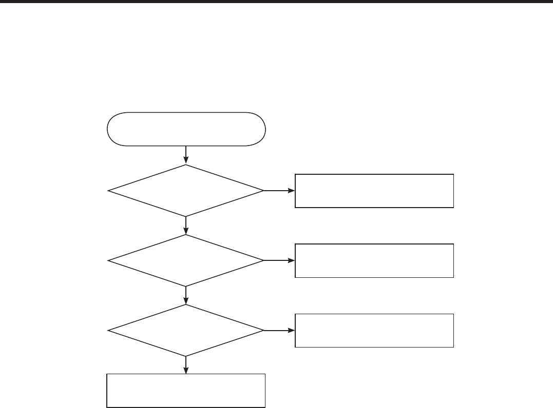
- 97 -
Copyright © 2010 LG Electronics. Inc. All right reserved.
Only for training and service purposes
LGE Internal Use Only
4. TROUBLE SHOOTING
START
TP1, TP2 Check the Sianal Change the main board
No
Yes
Change the main board
TP3 Check the Signal Change the Ear Jack
No
Yes
TP4 Check the Signal Change the U601
No
Yes
4.19.2 FM Trouble shooting
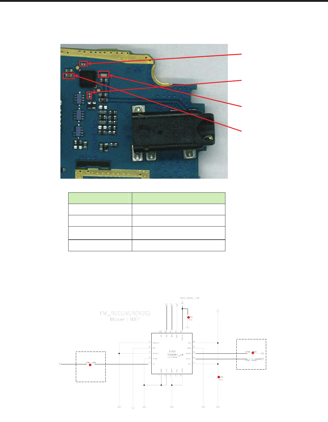
- 98 -
LGE Internal Use Only Copyright © 2010 LG Electronics. Inc. All right reserved.
Only for training and service purposes
4. TROUBLE SHOOTING
㝘⪌HG 㵬㦤G 㠄⸬㡸G 㵲㡸G ㍌G 㛺㏩⏼␘UU㝘⪌HG 㵬㦤G 㠄⸬
㡸G 㵲㡸G ㍌G 㛺㏩⏼␘UG G
G
TP# TP description
TP1 VREG_MSMP_2.6V
TP2 VREG_MSME_1.8V
TP3 FM_ANT_IN
TP4 FM_OUT_AUDIO signal
XUXU
X
{wYG
{wZG
{w[G
VREG_MSME_1V8
VREG_MSMP_2V6
K2
3_
C
TR
FM_R
L
CS
_
C2
I_
M
F_
D
UA
_C
I
UM
ADS_C2I_MF_DUA_CIUM
FM_L
FM_ANT
Close to QSC
Close to ANT
TP2
TP4
TP1
TP3
TP1
TP2
TP3
TP4
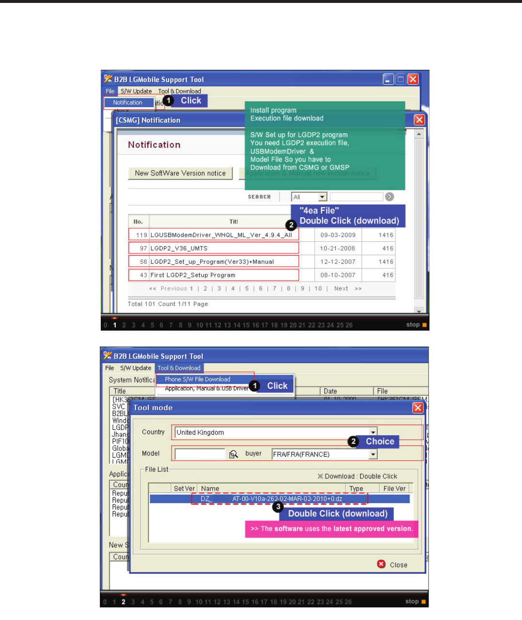
- 99 -
Copyright © 2010 LG Electronics. Inc. All right reserved.
Only for training and service purposes
LGE Internal Use Only
5. DOWNLOAD
5. DOWNLOAD
- 164 -
LGE Internal Use Only Copyright © 2010 LG Electronics. Inc. All right reserved.
Only for training and service purposes
5. DOWNLOAD
5. DOWNLOAD
LG-C320
LG-C320
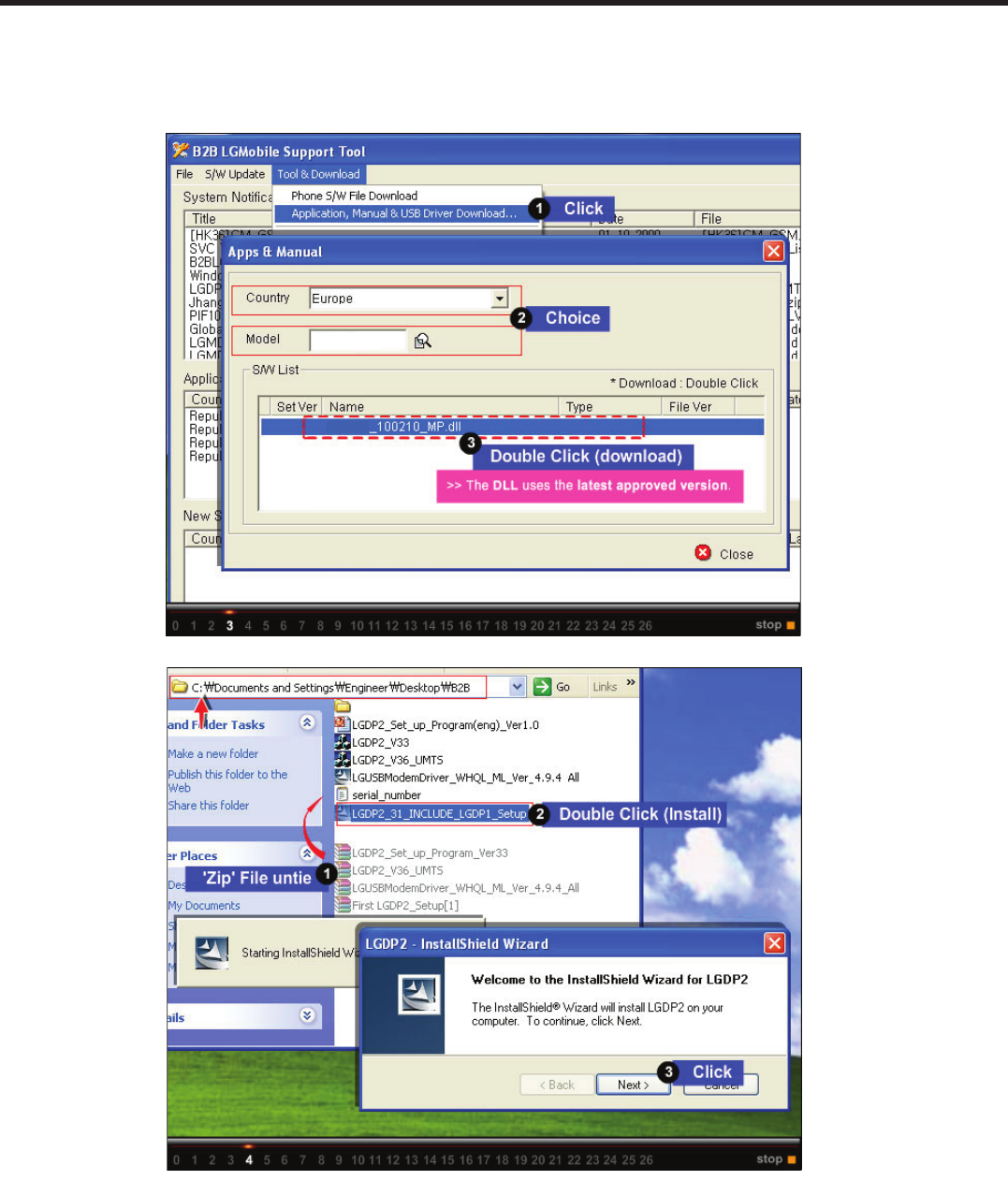
- 100 -
LGE Internal Use Only Copyright © 2010 LG Electronics. Inc. All right reserved.
Only for training and service purposes
- 165 -
Copyright © 2010 LG Electronics. Inc. All right reserved.
Only for training and service purposes
LGE Internal Use Only
5. DOWNLOAD
LG-C320
LG-C320
LG-C320
5. DOWNLOAD
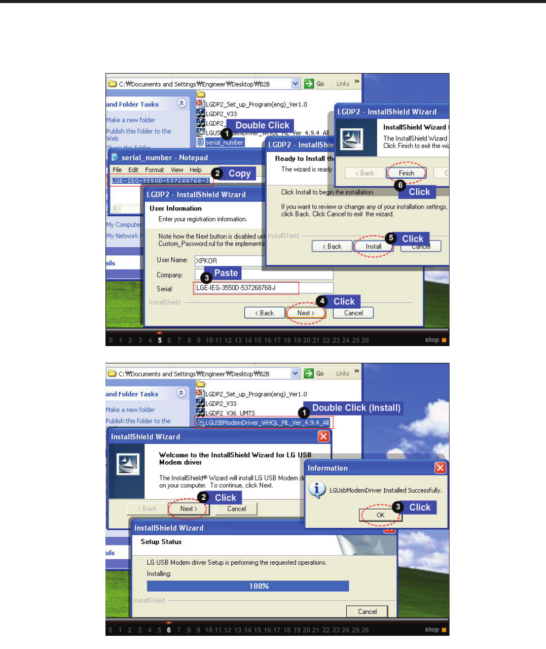
- 101 -
Copyright © 2010 LG Electronics. Inc. All right reserved.
Only for training and service purposes
LGE Internal Use Only
- 166 -
LGE Internal Use Only Copyright © 2010 LG Electronics. Inc. All right reserved.
Only for training and service purposes
5. DOWNLOAD
LG-C320
LG-C320
5. DOWNLOAD
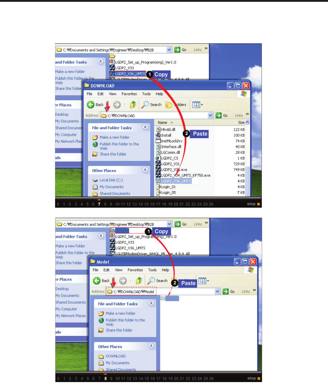
- 102 -
LGE Internal Use Only Copyright © 2010 LG Electronics. Inc. All right reserved.
Only for training and service purposes
- 167 -
Copyright © 2010 LG Electronics. Inc. All right reserved.
Only for training and service purposes
LGE Internal Use Only
5. DOWNLOAD
LG-C320
LG-C320
LG-C320
5. DOWNLOAD
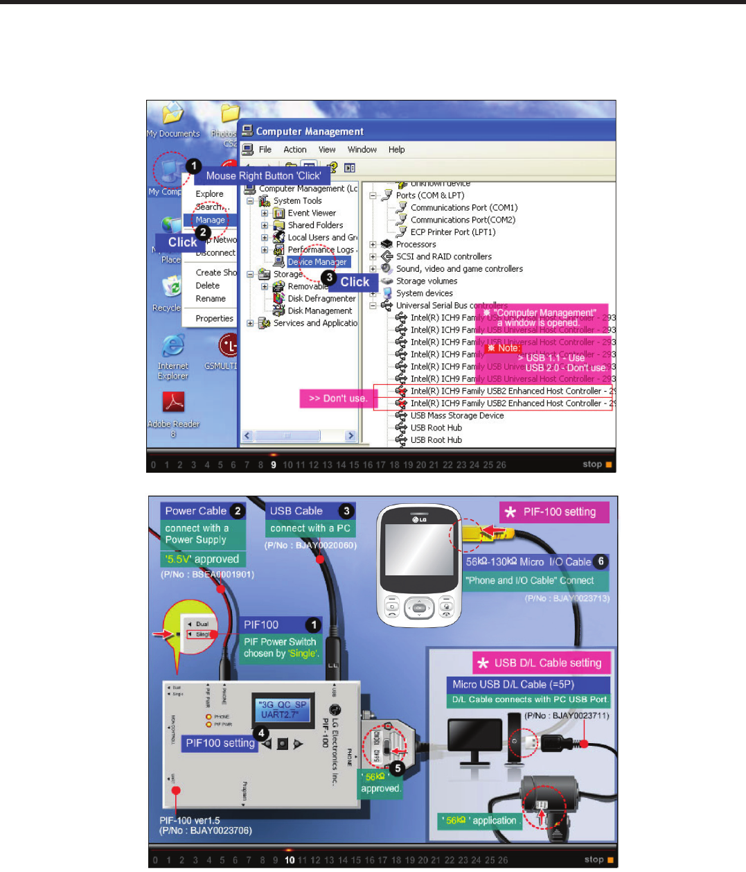
- 103 -
Copyright © 2010 LG Electronics. Inc. All right reserved.
Only for training and service purposes
LGE Internal Use Only
- 168 -
LGE Internal Use Only Copyright © 2010 LG Electronics. Inc. All right reserved.
Only for training and service purposes
5. DOWNLOAD
LG-C320
5. DOWNLOAD
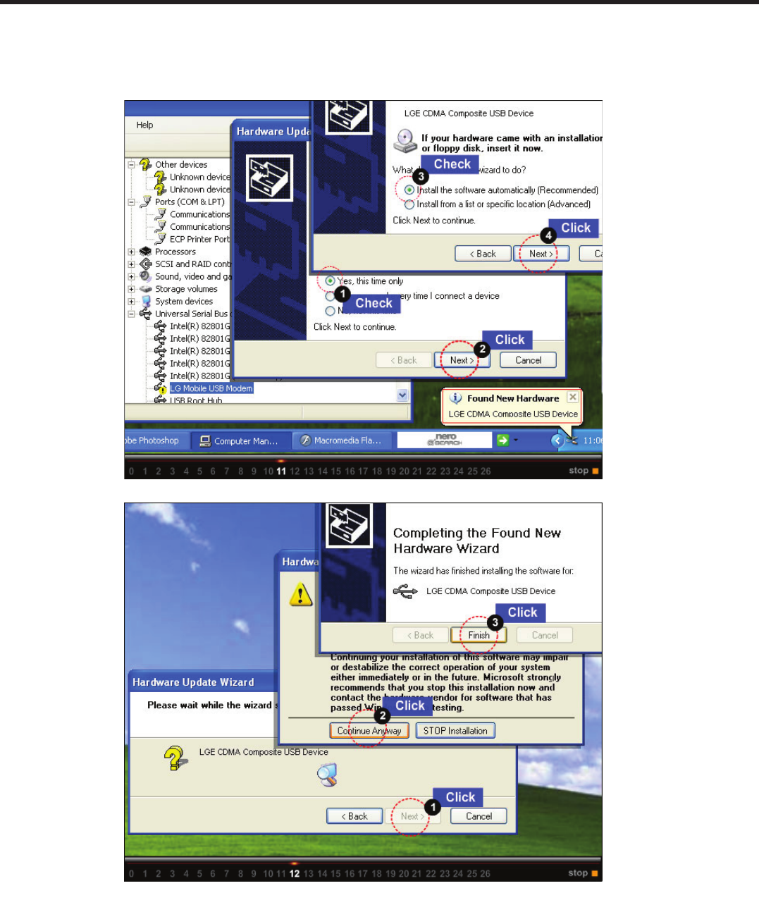
- 104 -
LGE Internal Use Only Copyright © 2010 LG Electronics. Inc. All right reserved.
Only for training and service purposes
- 169 -
Copyright © 2010 LG Electronics. Inc. All right reserved.
Only for training and service purposes
LGE Internal Use Only
5. DOWNLOAD
5. DOWNLOAD
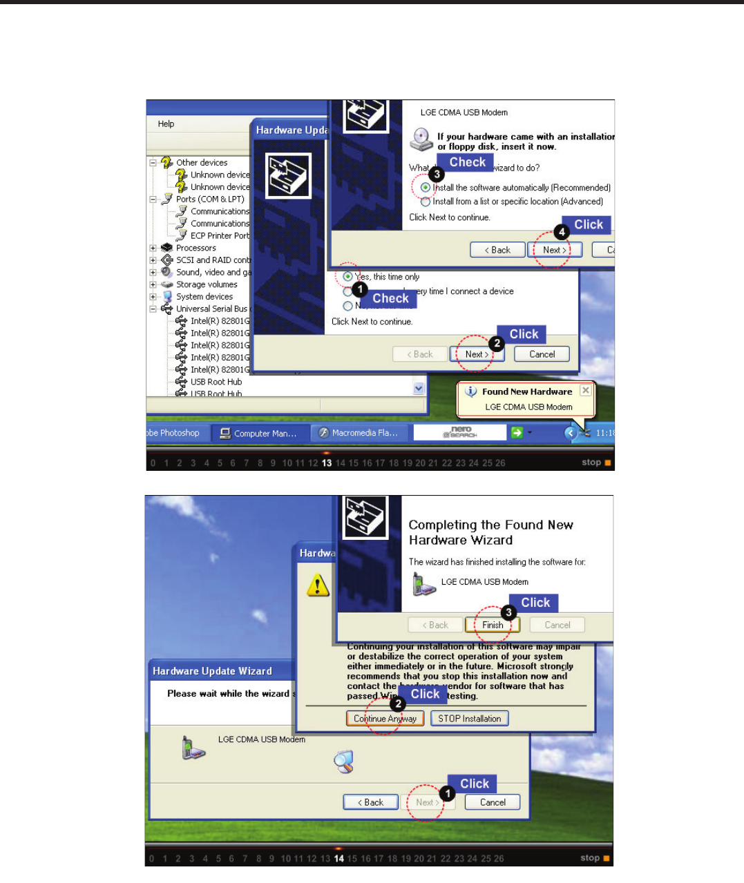
- 105 -
Copyright © 2010 LG Electronics. Inc. All right reserved.
Only for training and service purposes
LGE Internal Use Only
- 170 -
LGE Internal Use Only Copyright © 2010 LG Electronics. Inc. All right reserved.
Only for training and service purposes
5. DOWNLOAD
5. DOWNLOAD
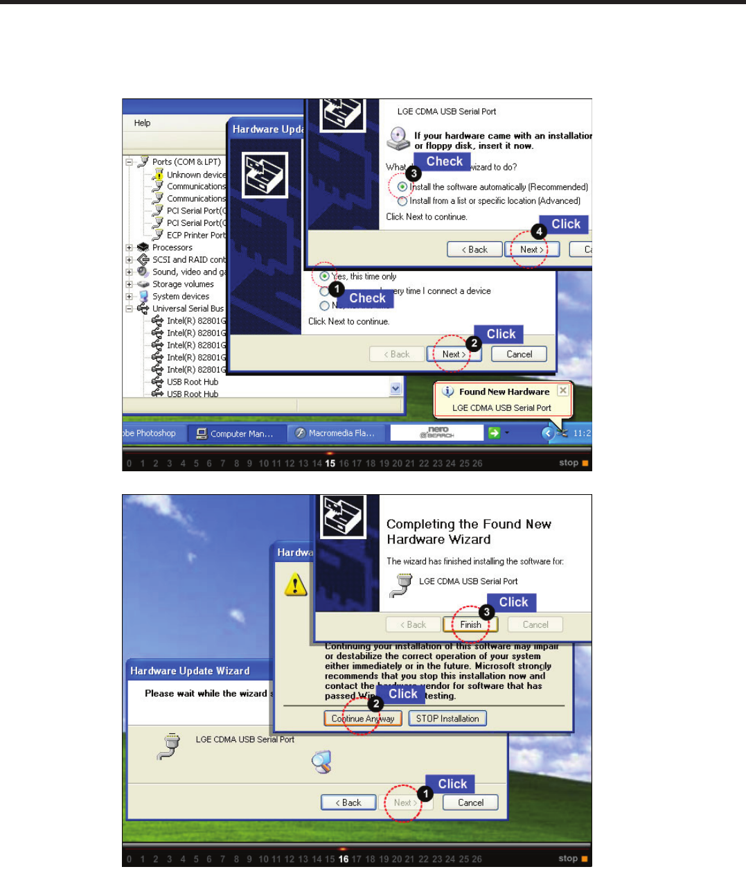
- 106 -
LGE Internal Use Only Copyright © 2010 LG Electronics. Inc. All right reserved.
Only for training and service purposes
- 171 -
Copyright © 2010 LG Electronics. Inc. All right reserved.
Only for training and service purposes
LGE Internal Use Only
5. DOWNLOAD
5. DOWNLOAD
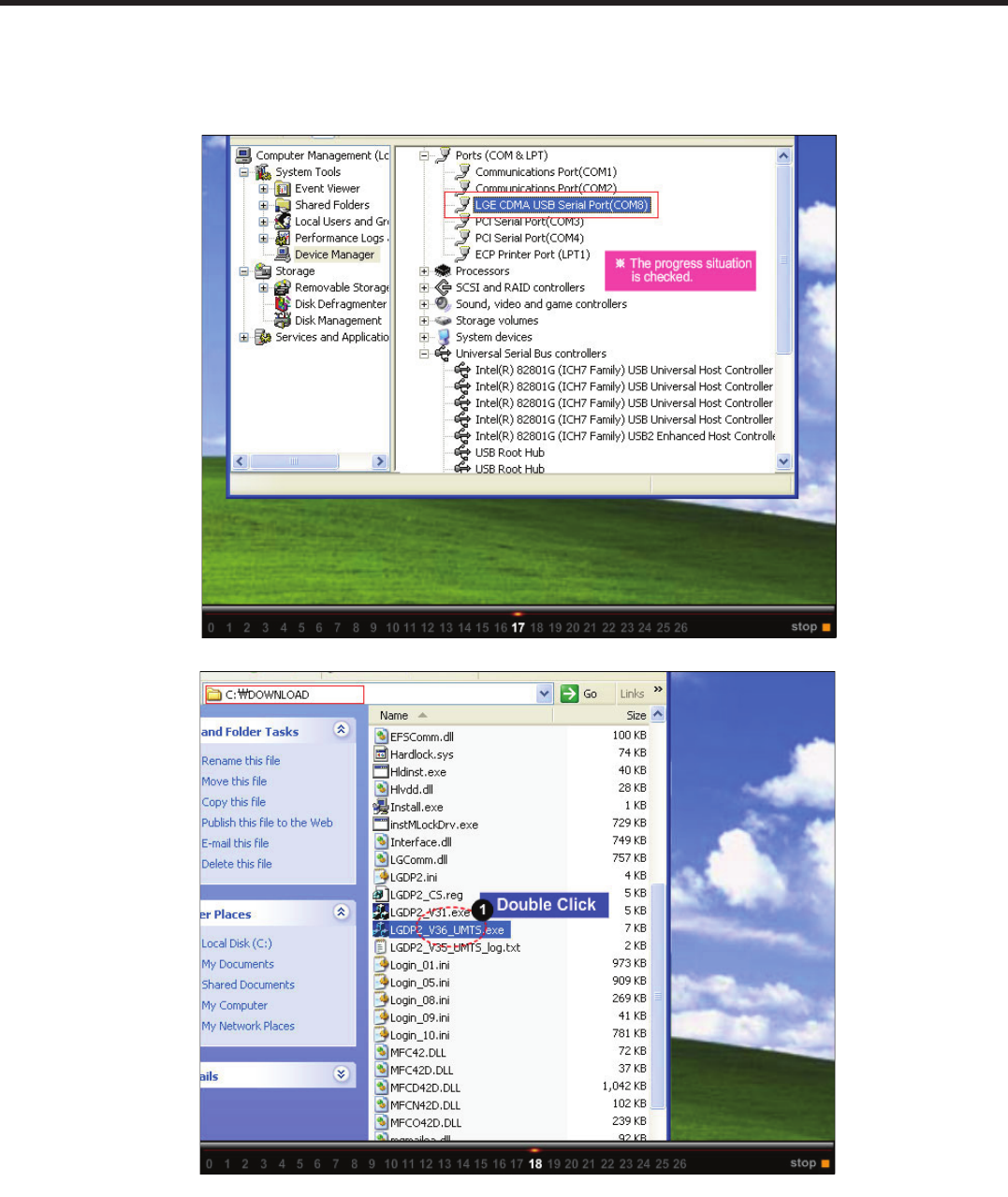
- 107 -
Copyright © 2010 LG Electronics. Inc. All right reserved.
Only for training and service purposes
LGE Internal Use Only
- 172 -
LGE Internal Use Only Copyright © 2010 LG Electronics. Inc. All right reserved.
Only for training and service purposes
5. DOWNLOAD
5. DOWNLOAD
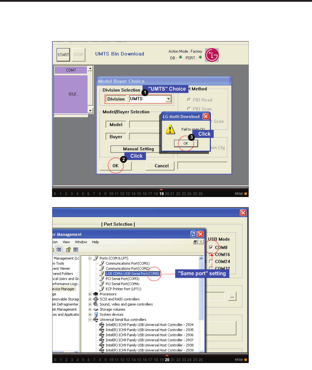
- 108 -
LGE Internal Use Only Copyright © 2010 LG Electronics. Inc. All right reserved.
Only for training and service purposes
- 173 -
Copyright © 2010 LG Electronics. Inc. All right reserved.
Only for training and service purposes
LGE Internal Use Only
5. DOWNLOAD
5. DOWNLOAD
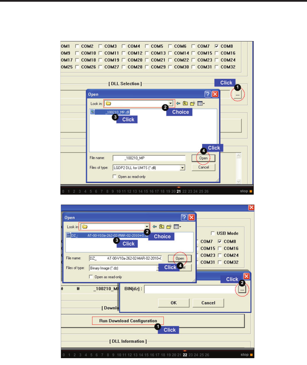
- 109 -
Copyright © 2010 LG Electronics. Inc. All right reserved.
Only for training and service purposes
LGE Internal Use Only
- 174 -
LGE Internal Use Only Copyright © 2010 LG Electronics. Inc. All right reserved.
Only for training and service purposes
5. DOWNLOAD
LG-C320
LG-C320
LG-C320
LG-C320
LG-C320
LG-C320
LG-C320LG-C320
5. DOWNLOAD
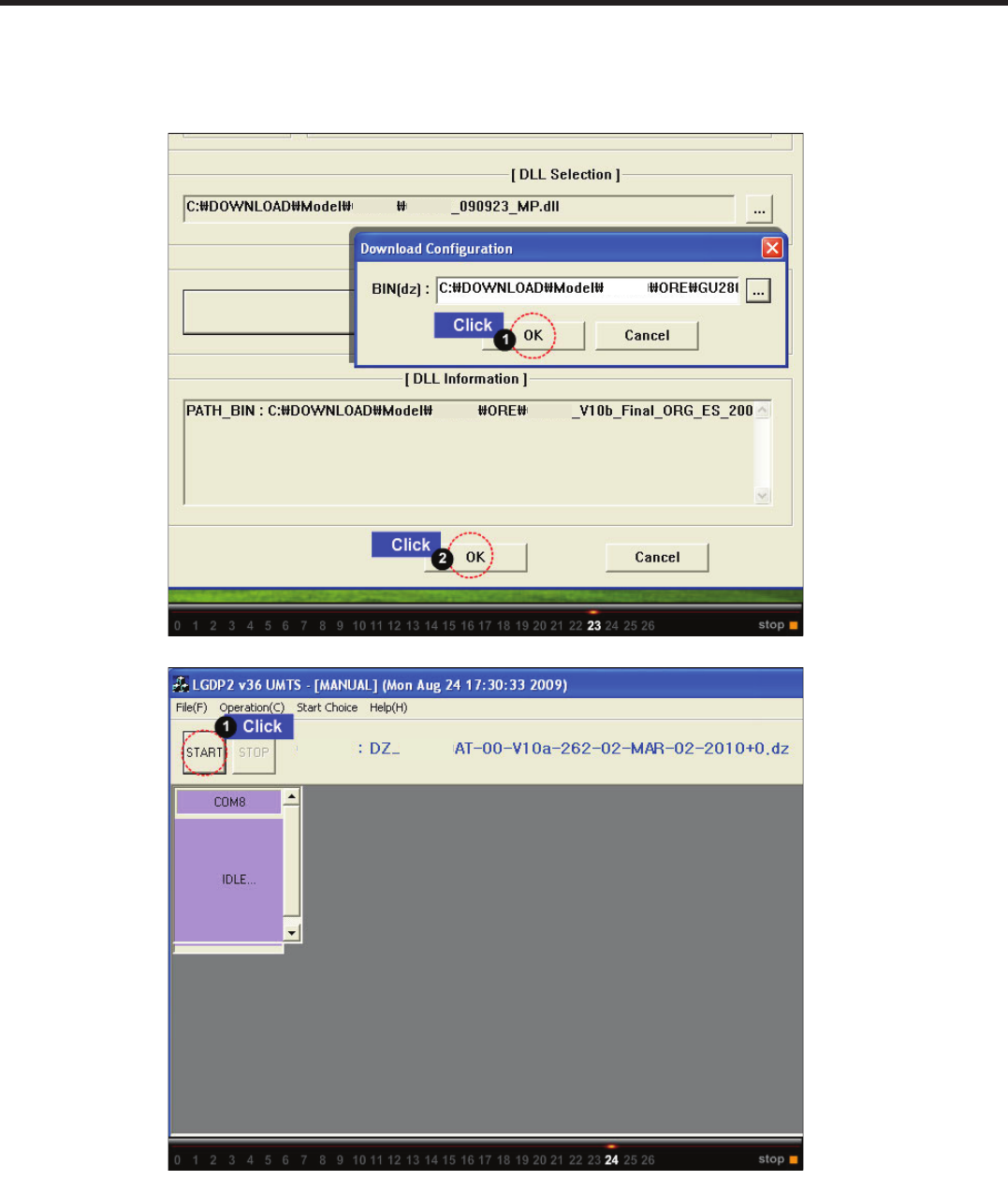
- 110 -
LGE Internal Use Only Copyright © 2010 LG Electronics. Inc. All right reserved.
Only for training and service purposes
- 175 -
Copyright © 2010 LG Electronics. Inc. All right reserved.
Only for training and service purposes
LGE Internal Use Only
5. DOWNLOAD
LG-C320 LG-C320
LG-C320 LG-C320
LG-C320
LG-C320
LG-C320
5. DOWNLOAD
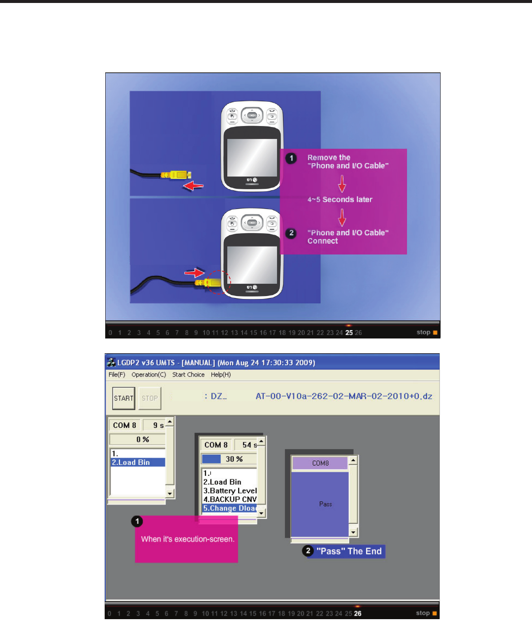
- 111 -
Copyright © 2010 LG Electronics. Inc. All right reserved.
Only for training and service purposes
LGE Internal Use Only
- 176 -
LGE Internal Use Only Copyright © 2010 LG Electronics. Inc. All right reserved.
Only for training and service purposes
5. DOWNLOAD
LG-C320
LG-C320
LG-C320
LG-C320
5. DOWNLOAD
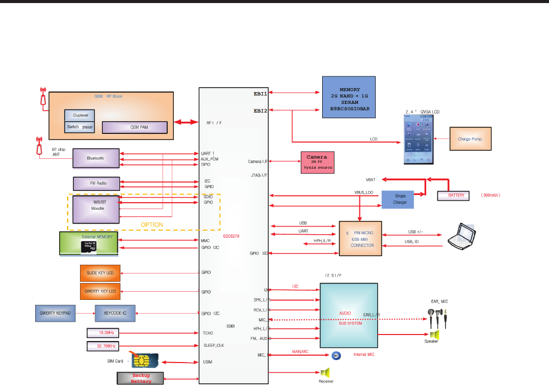
- 112 -
LGE Internal Use Only Copyright © 2010 LG Electronics. Inc. All right reserved.
Only for training and service purposes
6. BLOCK DIAGRAM
6. BLOCK DIAGRAM
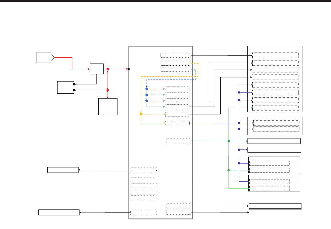
- 113 -
Copyright © 2010 LG Electronics. Inc. All right reserved.
Only for training and service purposes
LGE Internal Use Only
6. BLOCK DIAGRAM
ESC6270_BB/RF
ESC6270 POWER
51#F653#KZ#Eorfn#Gldjudp#=#Srzhu#b4#
VDD_CORE
VREG_MSMC_1V2
TA (5PIN)
5.1V,700mA
VBAT
Charger IC
USB_VBUS
ESC6270
_
POWER
VSW_RF2 ( 500mA)
VSW_MSMC ( 500mA)
VSW_RF1 ( 500mA) VDD_RFRX
VDD_RFTX
VREG_RFRX2_1V3
VREG_RFTX2_1V3
MU_IC VREG_MPLL (150mA)
VREG CDC2 (150mA)
VDD_P1
VDD_P2
VDD_RFA
VREG_RFA_2V2 VREG_RF1_2V3
VREG_RF2_1V4
VBUS_LDO_4.9V
VBAT
Battery
900mAh
VREG_RFA (300mA)
VREG
_
CDC2 (150mA)
VREG_RX2 (150mA)
VREG_TX2 (150mA)
VDD_P5
VDD_P6
VREG_MSME_1V8
VREG MSMP 2V6
MCP
SDRAM (1.8V , MAX 180mA )
NAND (1.8V , MAX 30mA )
VREG_MSME (300mA)
_
_
KEYCODE IC(1.8V, ?mA)
HALL IC(1.8V, )
VREG_MSMP ( 300mA)
FM RADIO
VREG_GP1 (150mA)
BT only MODULE
1.8V(, mA
1.8V(, mA
2.6V( , mA
VIB_DRV_N
MOTOR MOTOR_POWER_N
MICRO SD slot
(3 0V MAX mA )
VREG_TCXO ( 50mA)
VREG GP2 ( 300mA)
VREG_USB_2.6V ( 50mA)
VREG_USB_3.3V ( 50mA)
VREG_MICROSD_3V0
2.6V( , mA
BACKUP Battery VCOIN (3.0V, )
VCOIN
USIM SLOT (2.85V )
VREG_USIM_2V85
MICRO SD slot
(3
.
0V
, ,
MAX
mA
)
VREG_USIM (150mA)
VREG
_
GP2 ( 300mA)
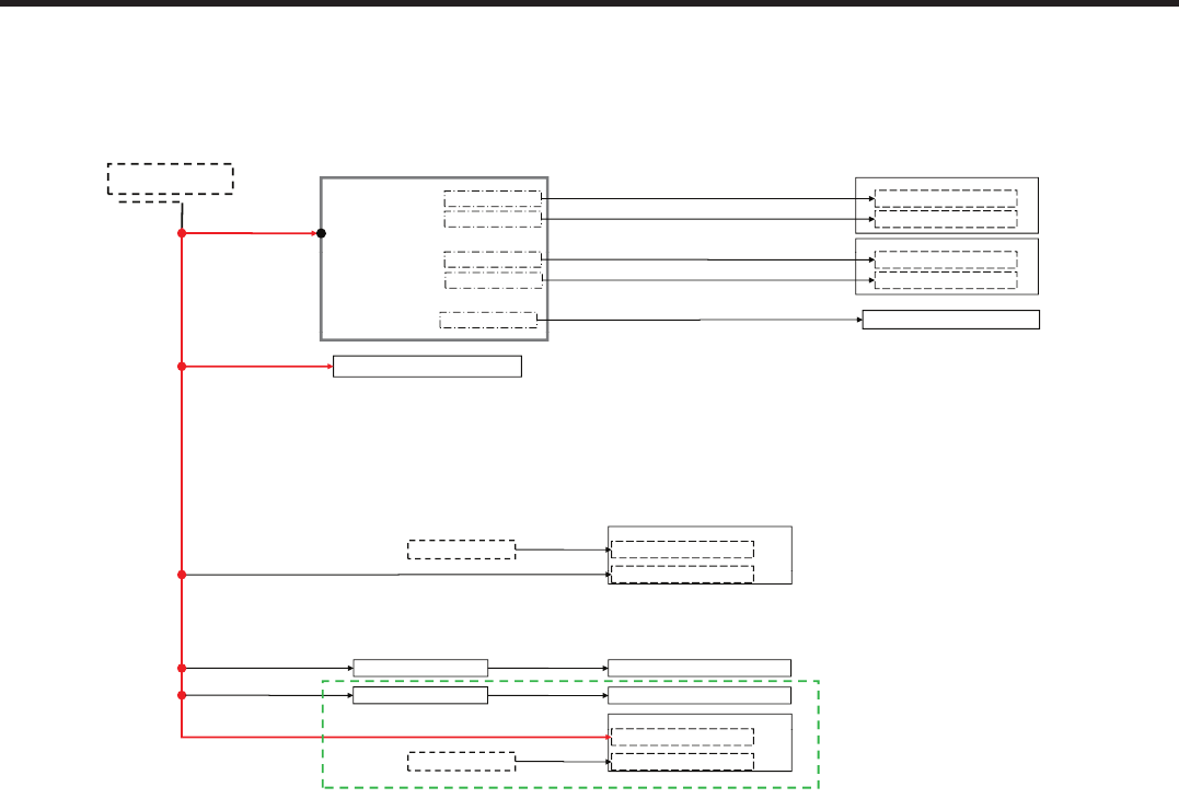
- 114 -
LGE Internal Use Only Copyright © 2010 LG Electronics. Inc. All right reserved.
Only for training and service purposes
6. BLOCK DIAGRAM
VBAT
51#F653#KZ#Eorfn#Gldjudp#=#Srzhu#b5#
VBAT
RT9396
(SUB PMIC)
LDO1(150m A )
LDO2( 150mA )
VLDO_CAM_2V8
VLDO_CAM_1V8
VLDO LCD 2V8
LCD_2.8V(, mA
LCD _1.8V( , mA
2.4” LCD MODULE
2MEGA CAMERA
WLED ( ,120mA )
WLEDOUT( 4.8V, 450mA )
LDO3(300m A )
VLDO_LCD_1V8
VLDO
_
LCD
_
2V8
LDO4( 500mA )
CAM_2.8V(, mA
CAM _1.8V( , mA
WLED_VOUT
GSM PAM (TQM7M5012)
VBAT
VBAT
VREG_MSME_1.8V
AUDIO SUB SYSTEM
1.8V(, mA
VDD
WIFI/BT/FM MODULE
WIFI_TCXO
LDO(150mA)
LDO(150mA) EAR_JACK DET.
VDD_TCXO
OPTION
WIFI(, mA
BT( , mA
VREG_MSMP_2V6
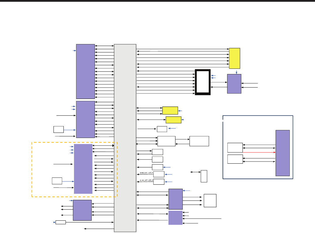
- 115 -
Copyright © 2010 LG Electronics. Inc. All right reserved.
Only for training and service purposes
LGE Internal Use Only
6. BLOCK DIAGRAM
EBI2_D ATA [0: 15]
NAND
CS1
N
61#F653#KZ#Eorfn#Gldjudp#=#EE
Memory
(H8BCS0SIOBAR)
NAND
_
CS1
_
N
EBI2 _ALE
EBI2 _CLE
EBI2_OE_N
EBI2_ WE_N
NAND _READY
RESOUT_N
SDRAM
DATA
[
0
:
31
]
VREG _MSME_1.8V
2M
CAMERA
CAM
_
MCLK
LCD _VSYNC_OUT
CAM_PCLK
CAM _DATA [2: 9]
CAM_HSYNC/VSYNC
MEGA _CAM_RESET _N
I 2C _SCL/SDA
From PMIC
MEGA _CAM _PWDN
VBAT
CAM_
2 Gb NAND
+
1 Gb SDRAM
SDRAM
_
DATA
[
0
:
31
]
SDRAM_ADDR [0:14]
SDRAM _CLK
SDRAM _CS_N(0)
SDRAM_ADV_N
SDRAM_ OE _N
SDRAM_WE_N
SDRAM _CLK (0)
LCD
EBI2_DATA [0: 15]
LCD_ MAKER _ID
EBI2_WE_N / EBI2_OE_N
LCD _CS_N
LCD_ADS
LCD_ RESET_N
LCD_IF_MODE
LCD _LDO_2.8 V
LCD
CHARGE
PUMP
WLED _1:3
MLED_OUT
VBAT
LDO_EN
From QSC
LCD _LDO_1.8 V
I2C_SDA , I2C_SCL
LDO
SDRAM _DQM[0 :3]
MICRO SD
CONNECTOR
BT _PCM_SYNC
BT
PCM
IN
BT_UART_ TXD
BT_UART_RXD
BT_UART_ CTS
BT_UART_RTS
MICROSD_ DATA [0: 3]
MICROSD_CMD/CLK
MICRO_DETECT_N
VREG_MICROSD_3.0V
BT _ANT
From BT chip ANT .
MSME_1.8V
MSMP_2.6V
QSC6270
SIM
CONNECTOR
USIM _DATA / CLK / RESET_ _N
VREG_USIM_2.85V
BLUE TOOTH
BT
_
PCM
_
IN
BT _PCM_OUT
BT _PCM_CLK
BT_WAKEUP _MSM
MSM_WAKEUP_BT
BT_ RESET_N
I2C COMM.
26
BT _ REG _ ON
KEYCODE
Crystal
MHZ
KEYCODE_INTERRUPT
KEYCODE RESET
32.768KHz
From SLEEP_CLK
Of QSC6270
QWERTY
KEY_ROW[0:7]
DC MOTOR VBAT
MOTOR DRIVE
32.768KHz
Oscillator
XTAL_IN
XTAL_OUT
19. 2MHz
XO
MMP_XTAL _OUT
QSC GPIO
MUIC_FM_AUDIO_I2C _SDA(GPIO49_P1_1.8V)
_SCL(GPIO 50_P1_1.8V )
MUIC /AUDIO
FM RADIO
MUIC_INT(GPIO 10_P1_ 1.8V)
I2C_SDA(GPIO 70_P3_2.85 V)
I2C _SCL(GPIO71_P 3_2.85V)
MUIC_FM_AUDIO_I2C
CP_
CP_
MSME_1.8V
MSMP_2.6V
IC
FM RADIO
Charge Pump
KEYCODE
__
RESET
KEYCODE__I2C
WLAN_SDIO[0:3]
WLAN_COMMEND
WLAN_CLK
BT _UART_ TXD
BT_UART _RXD
BT _UART_ CTS
VBAT
WLAN&BT ANT
KEY &
NAVI _KEY
KEY_COL[0:7]
JTAG
JTAG_TDI
JTAG_TCK
JTAG_TMS
JTAG_TDO
JTAG_TRST_N
JTAG_RTCK
HALL _IC
SLIDE_DETECT
VREG _MSME_1.8V
_
SLIDE KEY
LED VBAT
_
QWETY KEY
LED VBAT
WIFI &BT
MODULE
BT _PCM_SYNC
BT _PCM_IN
BT _PCM_OUT
BT _PCM_CLK
BT
_
UART
_
RTS
BT_WAKEUP _MSM
MSM_WAKEUP_BT
BT
RESET
N
26
Crystal
MHZ
32 768KH
WLAN&BT ANT
From WLAN&BT chip ANT .
AUDIO
SUB
S S
HP_EAR_R
HP_EAR_L
To. MMI CON.
I2C_SCL
I2C_SDA
MUIC_AUDIO_
I2C_SDA / SCL
MUIC_INT
BOOST_5V MUIC
USB_VBUS
USB+/-
USB _ID
5PIN
MICRO
MMI
CONN.
USB D +/-
UART1_RX/TX
VBAT
MUIC_AUDIO_
BT
_
RESET
_
N
BT_ REG _ ON
32
.
768KH
z
From SLEEP_CLK
Of QSC6270
OPTION
S
Y
S
TEM
( WM9093ECS-R )
SPK_R/L
HP_R/L
SPK +/-
MIC
MIC_BIAS
RCV R / L
FM
R ADIO
FM RADIO I2C MSME_1.8V
MSMP_2.6V
32.768KHz From SLEEP_CLK
Of QSC6270
FM ANT
FM RIGHT / LEFT
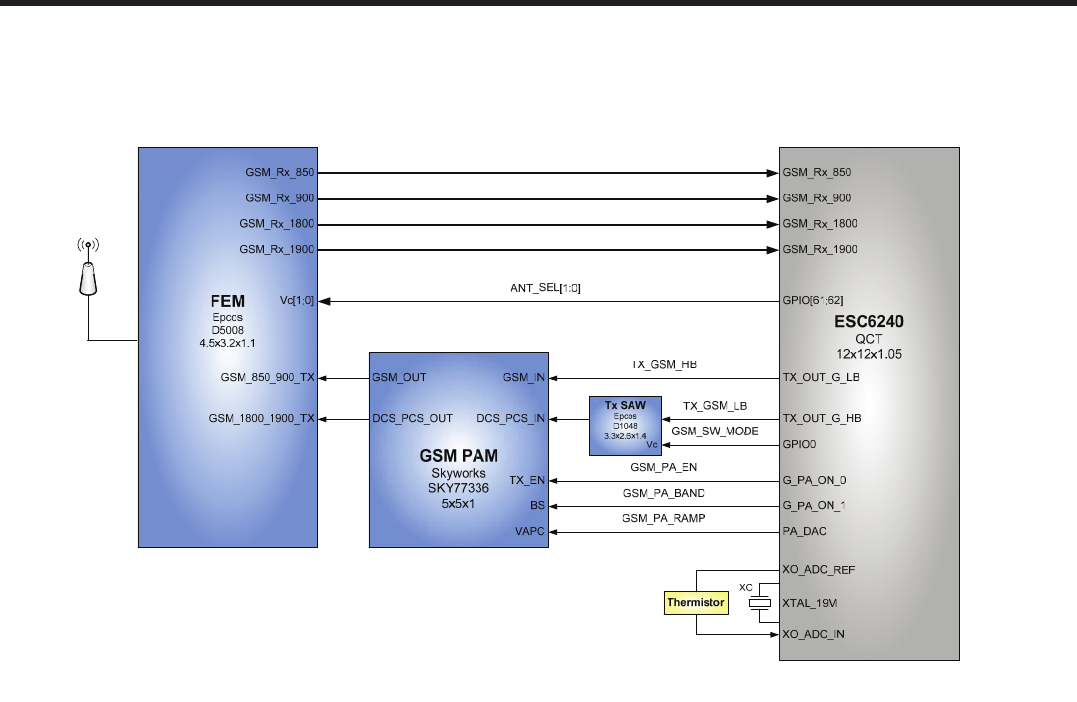
- 116 -
LGE Internal Use Only Copyright © 2010 LG Electronics. Inc. All right reserved.
Only for training and service purposes
6. BLOCK DIAGRAM
71#F653#KZ#Eorfn#Gldjudp#=#UIbJVP
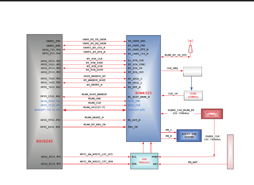
- 117 -
Copyright © 2010 LG Electronics. Inc. All right reserved.
Only for training and service purposes
LGE Internal Use Only
6. BLOCK DIAGRAM
81#F653#KZ#Eorfn#Gldjudp#=#Frqqhfwlylw|+EW2ZLIL2IP,brswlrq
VDD_TCXO
_
JACKEAR
_
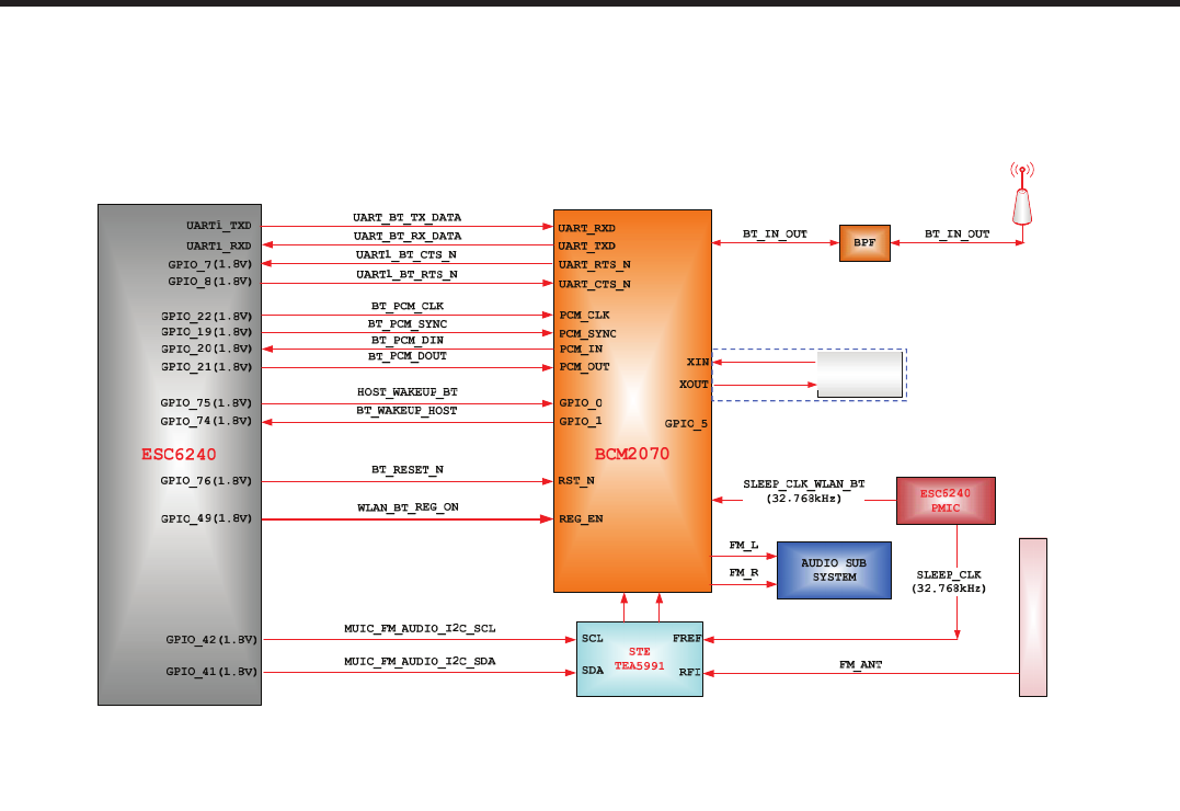
- 118 -
LGE Internal Use Only Copyright © 2010 LG Electronics. Inc. All right reserved.
Only for training and service purposes
6. BLOCK DIAGRAM
81#F653#KZ#Eorfn#Gldjudp#=#Frqqhfwlylw|+EW2IP,
E t l XO
E
x
t
erna
l XO
E
AR_JACK
E
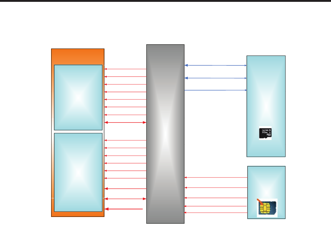
- 119 -
Copyright © 2010 LG Electronics. Inc. All right reserved.
Only for training and service purposes
LGE Internal Use Only
6. BLOCK DIAGRAM
91#F653#KZ#Eorfn#Gldjudp#=#Phpru|
HYNIX MCP
(H8BCSOSIOBAR)
M
SD D[0:3]
N
AND
_
_
CS
_
_
N
NAND_ LB_N
NAND_UB_N
N
AN
D
O
E
N
_CE
ALE
CLE
RE
_
MSD_CMD
MSD_CLK
NAND Flash
(2Gbit)
_
_
NAND_WE_N
NAND_BSY_N
NAND_WP_N
_
RE
_WE
RY_BY
_WP
External
Memory
(MICRO SD)
ESC6270
N
AN
D
_
D
ATA
[
0
:
1
5
]
IO[1:16]
DDR_M_CLK_N
CLK
SDRAM
D
DR
_
CKE[0]
_
DDR_CS[0]_N_
DDR_RAS_N
DDR_CAS_N
CKE
_CS
_RAS
CAS
SDRAM
(1Gbit)
D
DR
A
[0:13]
DDR_WE_N_ _
DDR_DQM[0:1]_
_
CAS
_WED
DQM USIM
(SIM PLUS)
SIM_CLK
_ _
S
IM
D
ATA
SIM_RST_N
_
DDR _ D[0:15]
ADDR
DQ
_
MUSIM_DM
MUSIM_DP
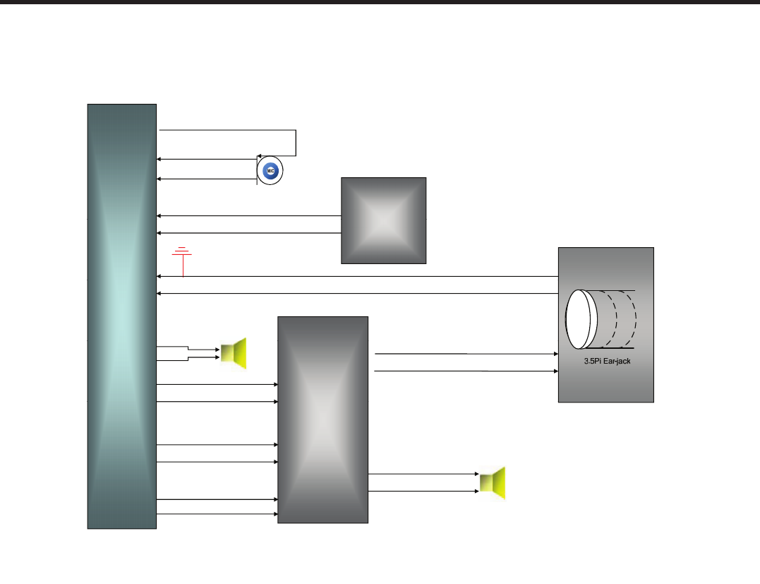
- 120 -
LGE Internal Use Only Copyright © 2010 LG Electronics. Inc. All right reserved.
Only for training and service purposes
6. BLOCK DIAGRAM
:1#F653#KZ#Eorfn#Gldjudp#=#Dxglr
HSED_BIAS
MIC1P
MICBIAS
MIC1P
MIC1P
MIC1N
LINE IN L P
MIC1N
FM_L
TEA5991
MIC2N
_ _ _
LINE_IN_R_N
MIC2N
FM_R
TEA5991
ESC6270
MIC2P
RXIN+
RCV+
MIC2P
HPH_OUT_L_P
RXIN+
RXIN-
IN1+
IN1
EAROP
EARON
RCV+
RCV- HPR
HPL
HS_OUT_R
HS_OUT_L
HS_L
HS_R
WM9093
IN2+
IN2
LINE_OUT_L_P
LINE OUT R N
HPH_OUT_R_N
IN1
-
SPK_P
SPK_N
IN2
-
LINE
_
OUT
_
R
_
N
GPIO
GPIO
SCL
SDA
SPK_OUT_P
SPK_OUT_N
MUIC_AUD_FM_I2C_SCL
OUT+
OUT-
MUIC_AUD_FM_I2C_SDA
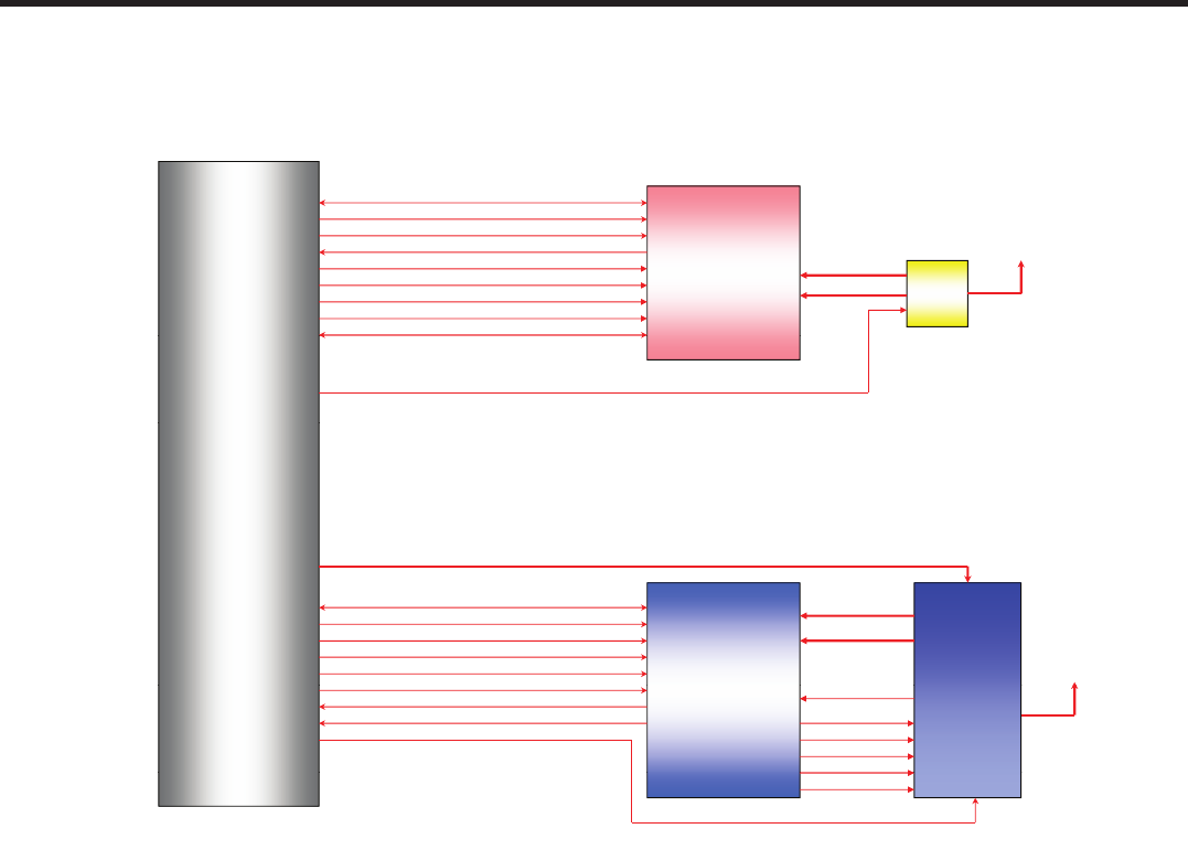
- 121 -
Copyright © 2010 LG Electronics. Inc. All right reserved.
Only for training and service purposes
LGE Internal Use Only
6. BLOCK DIAGRAM
;1#F653#KZ#Eorfn#Gldjudp#=#YLVXDO+#OFG#)#FDPHUD#,
CAM PCLK
CAM_MCLK
CAM_I2C_SCL
CAM_I2C_SDA
2M Camera
Hynics sensor
Bayer RGB Output
C2FK-H313P
CAM_DATA[0~7]
CAM_HSYNC
CAM_VSYNC
CAM_PWDN
CAM_RST_N
_
RT9396GQW
VBAT
VLDO_CAM_2V8
VLDO_CAM_1V8
BL_LCD_CAM_LDO_EN
QSC6270
LCD DATA[0~15]
VREG_MSMP_2.6V
2.4” TFT LCD
QVGA
LCD
_
DATA[0~15]
LCD_RS
LCD_RST_N
LCD_CS_N
LCD_WR_N
LCD RD
RT9396GQW
VLDO_LCD_2V8
VLDO_LCD_1V8
VBAT
CPU I/F
DM24-DSM04
LCD
_
RD
LCD_VSYNC_OUT
LCD_MAKER_ID
RT9396GQW
5channel
WLED_OUT
WLED2
WLED3
WLED4
WLED1
BL_LCD_CAM_LDO_EN
WLED5

- 122 -
LGE Internal Use Only Copyright © 2010 LG Electronics. Inc. All right reserved.
Only for training and service purposes
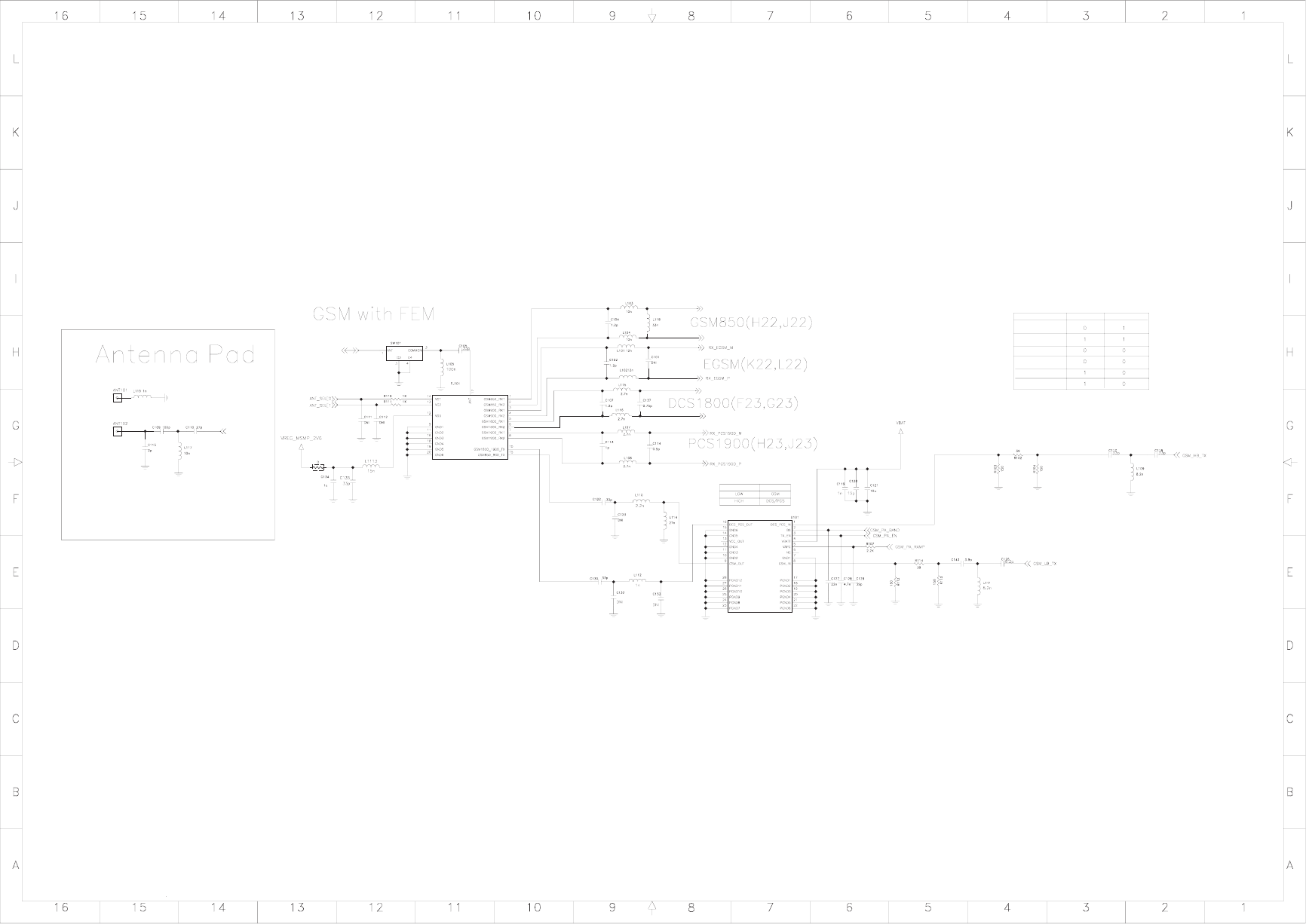
- 123 -
7. CIRCUIT DIAGRAM
LGE Internal Use OnlyCopyright © 2010 LG Electronics. Inc. All right reserved.
Only for training and service purposes
850, 900,1800,1900MHz
R109
ANT_FEED
ANT_FEED
RX_DCS1800_M
RX_DCS1800_P
RX_GSM850_M
RX_GSM850_P
ANTENNA SWITCH MODULE LOGIC
MODE
ANT_SEL1
GSM850/EGSM TX
PCN/PCS TX
GSM850 RX
EGSM RX
PCN RX
GSM_PA_BAND
6 dB
ANT_SEL0
PCS RX
6 dB
1-2-1-3_ESC-Quad EDGE
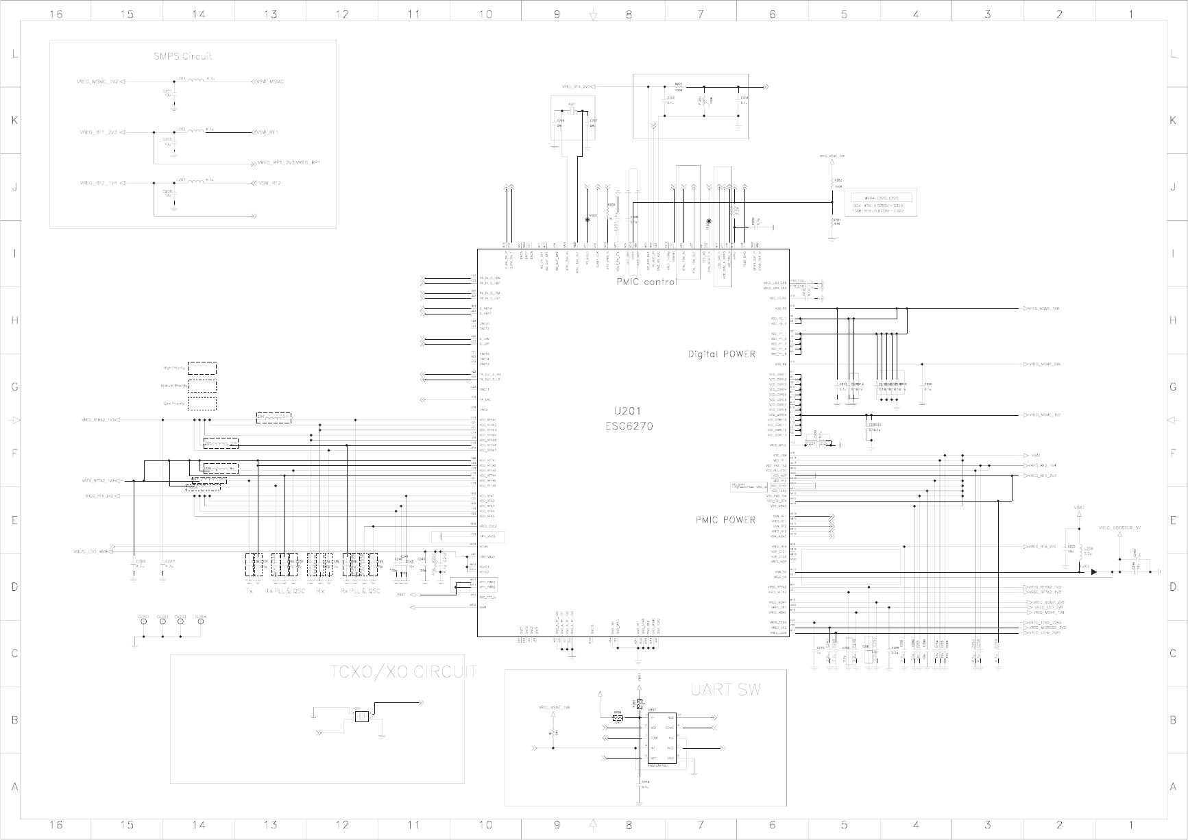
7. CIRCUIT DIAGRAM
- 124 -
LGE Internal Use Only Copyright © 2010 LG Electronics. Inc. All right reserved.
Only for training and service purposes
VBAT
19.2MHz
32.768KHz
VREG_MSMP_2V6
GSM_PA_RAMP
NE_AP_MSG
GND
DNAB_AP_MSG
GSM_LB_TX
GSM_HB_TX
N_NISER_MSM
DLOH_SP
VSW_RF1
VSW_RF2
VSW_MSMC
VREG_RFRX2_1V3
VREG_RFTX2_1V3
DEL_YEK_NIAM
VREG_RFA_2V2
NI_CDA_OX
XO_ADC_IN
K23_CTR
N_WSNO_MP
P_SAIB_CIMV
VCOIN
VREG_RF1_2V3|VREG_RF1
VREG_RF2_1V4|VREG_RF2
VREG_RF2_1V4|VREG_RF2
UART_TX
CDA_KOOH
RX_EGSM_M
RX_EGSM_P
RX_PCS1900_M
RX_PCS1900_P
RX_DCS1800_M
RX_DCS1800_P
RX_GSM850_M
RX_GSM850_P
DEL_YEK_EDILS
N_REWOP_ROTOM
XTAL_19M_OUT
TUO_M91_LATX
XTAL_19M_IN
NI_M91_LATX
TP_UART_TX
TP_UART_RX
BT_UART_RX
BT_UART_TX
UART_RX
DI_TAB
UART_BT_SW
- Normal Audio Power : +VPWR
2-2-2-1_ESC_ESC6270
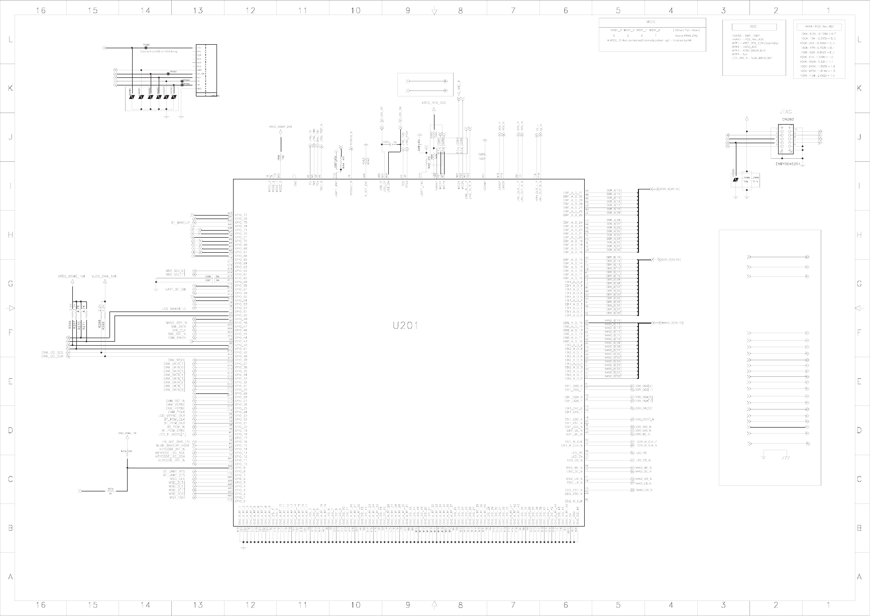
- 125 -
7. CIRCUIT DIAGRAM
LGE Internal Use OnlyCopyright © 2010 LG Electronics. Inc. All right reserved.
Only for training and service purposes
VREG_MSME_1V8
12
11
10
9
8
7
6
5
4
3
2
1GND
RX
TX
VCHAR
ON_SW
VBAT
PWR
URXD
UTXD
3G2.5G
DNG_SH
HS_GND|GND
MAIN_MIC_GND|GND
DNG_CIM_NIAM
VBAT
MSM_RESIN_N
PS_HOLD
UART_BT_SEL
UART_BT_SEL
PM_ONSW_N
MUIC_INT_N
JTAG_RTCK
JTAG_TCK
JTAG_TDI
JTAG_TDO
JTAG_TMS
JTAG_TRST_N
NAND_OE_N|LCD_RD
CHG_EN_N
BT_WAKEUP_HOST
RESOUT_N|NAND_WP_N
DDR_A[14]|DDR_BA[00]
DDR_A[15]|DDR_BA[01]
XT_TRAU
NAND_D[00]|LCD_DATA[0]
NAND_D[01]|LCD_DATA[1]
NAND_D[02]|LCD_DATA[2]
NAND_D[03]|LCD_DATA[3]
NAND_D[04]|LCD_DATA[4]
NAND_D[05]|LCD_DATA[5]
NAND_D[06]|LCD_DATA[6]
NAND_D[07]|LCD_DATA[7]
NAND_D[08]|LCD_DATA[8]
NAND_D[09]|LCD_DATA[9]
NAND_D[10]|LCD_DATA[10]
NAND_D[11]|LCD_DATA[11]
NAND_D[12]|LCD_DATA[12]
NAND_D[13]|LCD_DATA[13]
NAND_D[14]|LCD_DATA[14]
NAND_D[15]|LCD_DATA[15]
NAND_WE_N|LCD_WR_N
CHG_STS_N
HALL_SENS_DET
R_MF
MUIC_AUD_FM_I2C_SCL
MUIC_AUD_FM_I2C_SDA
BL_LCD_CAM_LDO_I2C_SCL
L_MF
USB_VBUS
HS_JACK_DET
WLAN_BT_REG_ON
WLAN_CLK
LCD_IF_MODE[0]
BL_LCD_CAM_LDO_I2C_SDA
WLAN_RST_N
BL_LCD_CAM_LDO_EN
BT_RST_N
WLAN_CMD
LCD_RST_N
P_CIM_NIAM
WLAN_SDIO[3]
WLAN_SDIO[0]
WLAN_SDIO[1]
WLAN_SDIO[2]
TP_UART_TX
TP_UART_RX
XR_TRAU
BT_PWR_ON
MUSIM_DM
MUSIM_DP
Low : UART Comm
High : BT UART
NET Conn
2-2-2-1_ESC_ESC6270
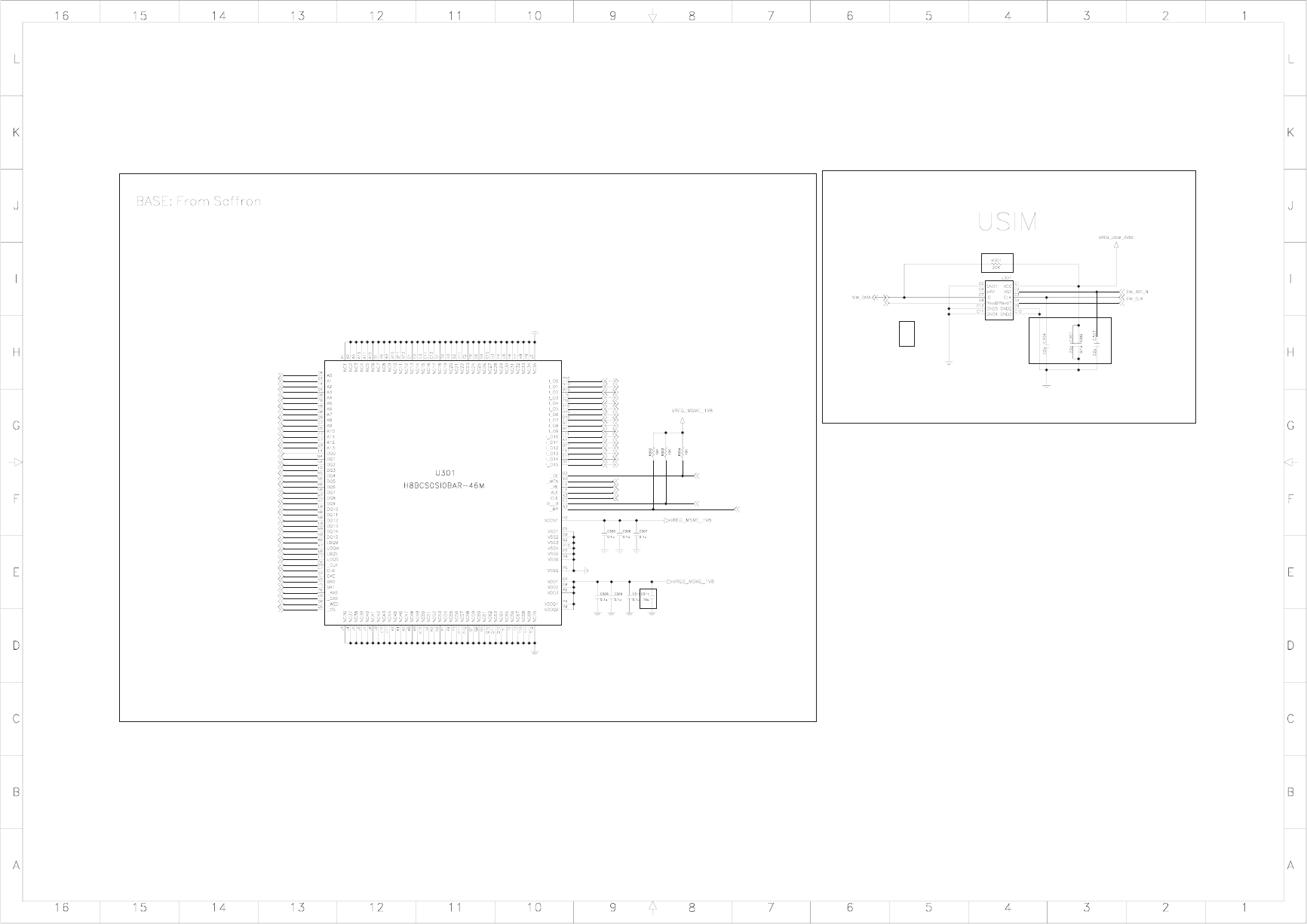
7. CIRCUIT DIAGRAM
- 126 -
LGE Internal Use Only Copyright © 2010 LG Electronics. Inc. All right reserved.
Only for training and service purposes
DDR_D[00]
DDR_M_CLK_N
NAND_BSY_N
DDR_DQM[1]
NAND_UB_N
NAND_OE_N
NAND_LB_N
NAND_CS_N
DDR_WE_N
DDR_CAS_N
DDR_DQS[1]
DDR_DQS[0]
DDR_DQM[0]
DDR_CS[0]_N
DDR_CKE[0]
DDR_D[09]
DDR_D[08]
DDR_D[07]
DDR_D[06]
DDR_D[05]
DDR_D[04]
DDR_D[03]
DDR_A[13]
DDR_A[12]
DDR_A[11]
DDR_A[10]
DDR_A[09]
DDR_A[08]
DDR_A[07]
DDR_A[06]
DDR_A[05]
DDR_A[04]
DDR_D[02]
DDR_A[03]
DDR_A[02]
DDR_D[14]
DDR_D[13]
DDR_D[12]
DDR_D[11]
DDR_D[10]
DDR_D[01]
DDR_RAS_N
DDR_A[01]
DDR_A[00]
NAND_WP_N
DDR_BA[00]
DDR_BA[01]
DDR_D[15]
NAND_D[00]
NAND_D[01]
NAND_D[02]
NAND_D[03]
NAND_D[04]
NAND_D[05]
NAND_D[06]
NAND_D[07]
NAND_D[08]
NAND_D[09]
NAND_D[10]
NAND_D[11]
NAND_D[12]
NAND_D[13]
NAND_D[14]
NAND_D[15]
NAND_WE_N
DDR_M_CLK_P
MUSIM_DM MUSIM_DP
MCP2-1_2G_1G DDRx16_hynix
ENSY0024301
3-3-1_6P_USIM
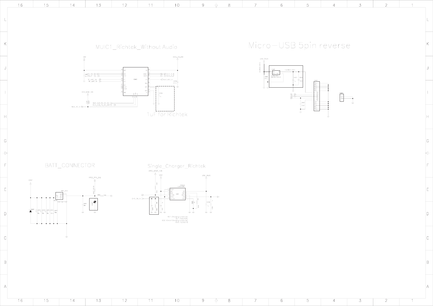
- 127 -
7. CIRCUIT DIAGRAM
LGE Internal Use OnlyCopyright © 2010 LG Electronics. Inc. All right reserved.
Only for training and service purposes
VBUS_LDO_4V9
IND
CHG_STS_N
MUIC_IO_M
MUIC_IO_P
MUIC_ACC_ID
BAT_ID
4-2-3-2
4-2-1-4
4-3-1-3
4-5-2-1
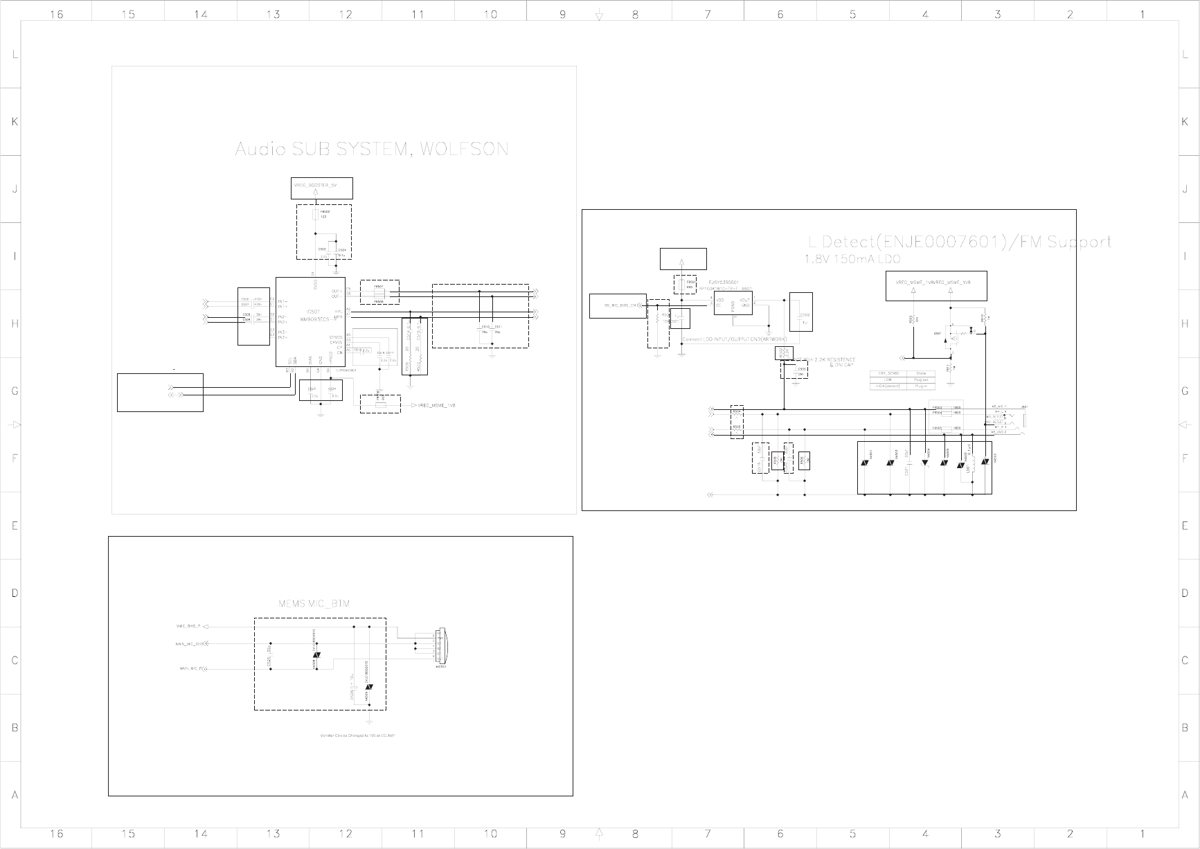
7. CIRCUIT DIAGRAM
- 128 -
LGE Internal Use Only Copyright © 2010 LG Electronics. Inc. All right reserved.
Only for training and service purposes
VREG_MSMP_2V6
GND
HS_GND
HS_R
SPK_N
SPK_P
MUIC_AUD_FM_I2C_SCL
MUIC_AUD_FM_I2C_SDA
SPK_OUT_N
SPK_OUT_P
HS_MIC_P|Hook_ADC
FM_ANT
HS_OUT_R
HS_OUT_R
HS_OUT_L
HS_OUT_L
HS_JACK_DET
HS_L
5-1-2-1
5-4-1-1
´ëüǰ : EUSY0407501
NC
RP183K181D is possible to 1.8 & 2.6 IO
WM9093 is possible to 1.8 & 2.6 IO When HPVDD is 1.8V
4-4-2-3
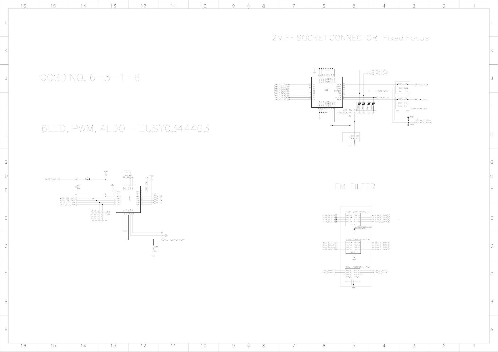
- 129 - LGE Internal Use OnlyCopyright © 2010 LG Electronics. Inc. All right reserved.
Only for training and service purposes
7. CIRCUIT DIAGRAM
01
5
64
73
82
91
01
5
64
73
82
91
01
5
64
73
82
91
R603
BL_LCD_CAM_LDO_I2C_SCL
BL_LCD_CAM_LDO_I2C_SDA
WLED1
6CH+4LDO,PWM
6-2-2-1
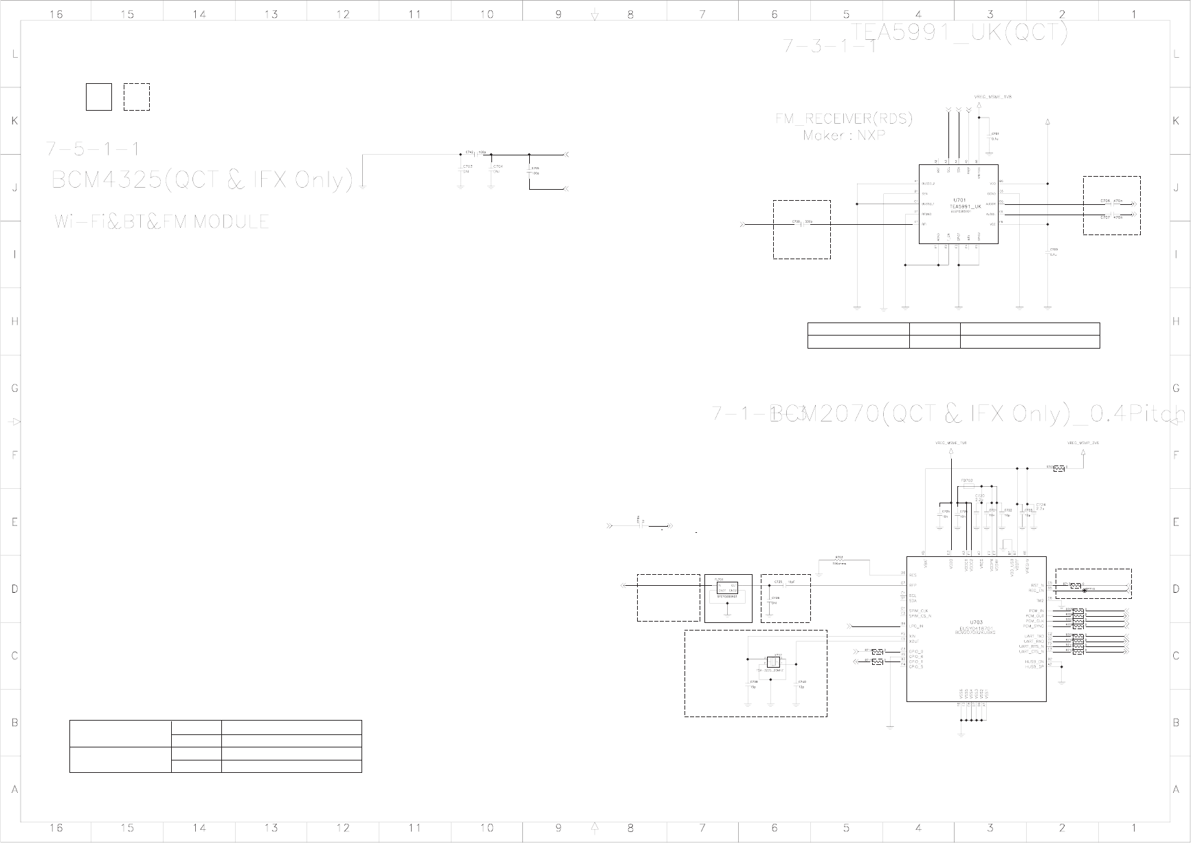
- 130 -
LGE Internal Use Only Copyright © 2010 LG Electronics. Inc. All right reserved.
Only for training and service purposes
VREG_MSME_1V8
VREG_MSMP_2V6
26MHz
A4
C4
E4
D4
K23_CTR
RTC_32K
BT_WAKEUP
BT_PCM_CLK
BT_PCM_OUT
BT_PCM_IN
BT_PCM_SYNC
BT_UART_RTS
BT_UART_CTS
BT_WAKEUP_HOST
FM_R
LCS_C2I_MF_DUA_CIUM
ADS_C2I_MF_DUA_CIUM
FM_L
FM_ANT
BT_RST_N
WLAN_BT_ANT_FEED
BT_ANT_FEED
BT_ANT_FEED
RTC_32K768
RTC_32K768
BT_UART_RX
BT_UART_TX
BT_PWR_ON
Close to QSC
Close to ANT
VFM_PWR
VREG_MSME_1V8 VREG_MSME_1V8
Connectivity_ANT_PAD
VFM_PWRQCT
QCT
must have 1% tolerance
can be removed
When power class 1.5 is used, R307 is populated and R308 is depopulated.
(Vice versa for power class 2)
Class 1.5
QCT
IFX
VBT_WIFI_IO_2V6
QCT
IFX
VBAT
VREG_MSMP_2V6
VBAT
VBAT
VPM_IO_2V62
7. CIRCUIT DIAGRAM
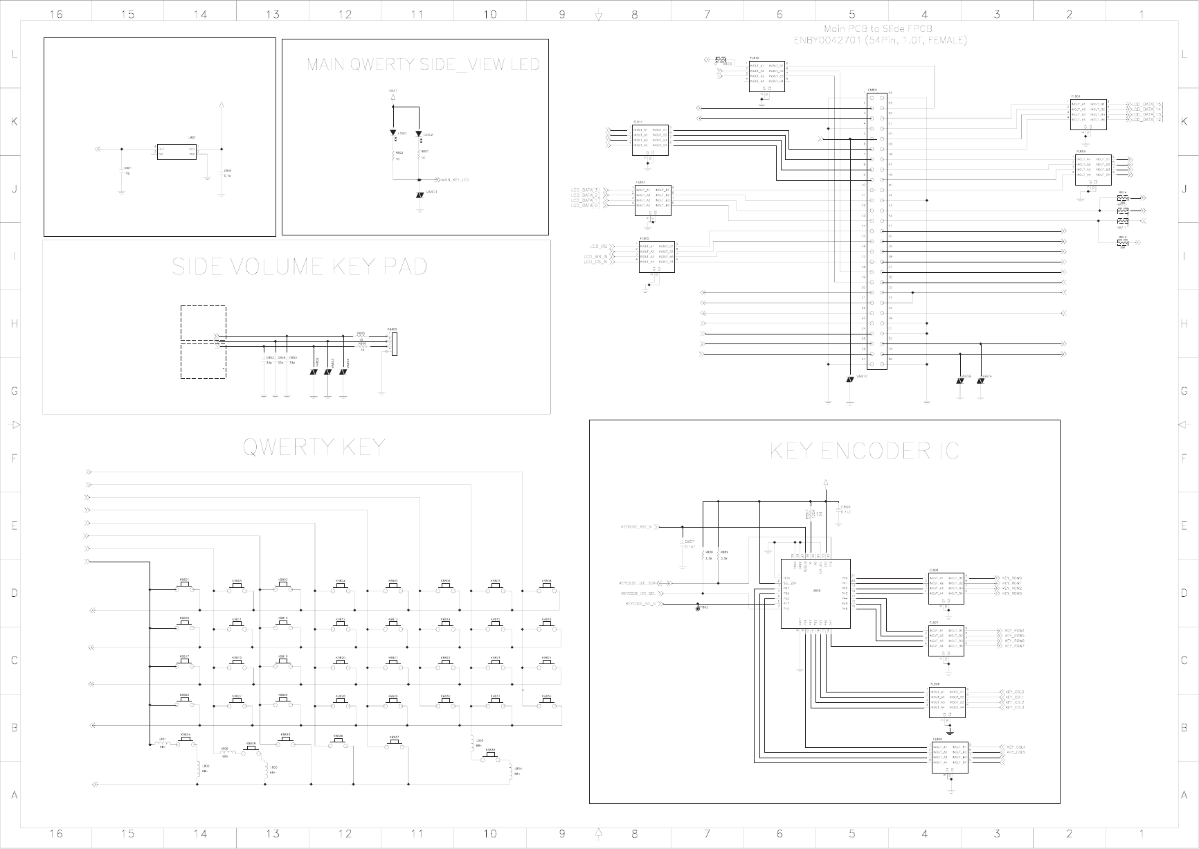
- 131 -
7. CIRCUIT DIAGRAM
LGE Internal Use OnlyCopyright © 2010 LG Electronics. Inc. All right reserved.
Only for training and service purposes
15pF
15pF
15pF
15pF
25pF
25pF
25pF
25pF
VREG_MSME_1V8
15pF
15pF
VREG_MSMP_2V6
GND
PM_ONSW_N
VREG_MSME_1V8
VCOIN
RCV_P
RCV_N
KEY_ROW0
KEY_ROW0
KEY_ROW1
KEY_ROW1
KEY_ROW2
KEY_ROW2
KEY_ROW3
KEY_ROW3
LCD_RD
LCD_DATA[4]
LCD_DATA[5]
LCD_DATA[6]
LCD_DATA[7]
LCD_DATA[8]
LCD_DATA[9]
LCD_DATA[10]
LCD_DATA[11]
HALL_SENS_DET
LCD_VSYNC_OUT
LCD_IF_MODE[1]
LCD_IF_MODE[0]
VLDO_LCD_1V8
VLDO_LCD_2V8
SLIDE_KEY_LED
WLED4
WLED5
KEY_COL7
KEY_COL7
KEY_COL6
KEY_COL6
KEY_COL5
LCD_RST_N
WLED1
WLED2
WLED3
WLED_VOUT
KEY_ROW7
KEY_ROW7
KEY_ROW5
KEY_ROW5
KEY_COL4
KEY_COL4
KEY_ROW6
KEY_COL3
KEY_COL0
KEY_COL1
KEY_COL2
KEY_ROW4
LCD_MAKER_ID
VREG_LCD_2V8
SYM
'&.
SPACE
@&/
?&:TEXT
SHIFTENTERM&;N&0
B&9V&8
"&,
C&7X&=Z&+
FNBACKL&}
PO&&
K&{J&#
H&6G&5F&4D&'
S&]
A&[
8-1-1-1
I&^U&*Y&3T&2R&1
E&%
W&$
Q
CAM
DOWN
UP
<Volume Up/Down>
7. CIRCUIT DIAGRAM
- 132 -
LGE Internal Use Only Copyright © 2010 LG Electronics. Inc. All right reserved.
Only for training and service purposes
VBAT
MOTOR_POWER_N
MSD_D[2]
MSD_D[3]
MSD_D[0]
MSD_D[1]
MSD_CMD
3-2-1-3_push_1.50T
- 133 -
7. CIRCUIT DIAGRAM
LGE Internal Use OnlyCopyright © 2010 LG Electronics. Inc. All right reserved.
Only for training and service purposes
KB105
KB101 KB102 KB103 KB104
KB109KB108KB107KB106
KB111KB110
LD103 LD104 LD105 LD108LD106 LD107
10
R107 R108
10 10
R105 R106
10 10
R109 R110
10
VA101
C102
0.1u0.1u
C101
VA102
16 15 14 13 12 11 10 9 87654321
L
K
J
I
H
G
F
E
D
C
B
A
L
K
J
I
H
G
F
E
D
C
B
A
16 15 14 13 12 11 10 9 87654321
CN102
35
34
33
32
31
30
29
28
27
26
25
24
23
22
21
20
19
18
17
16
15
14
13
12
11
10
9
8
7
6
5
4
3
2
1
CN101
2625
2724
2823
2922
3021
3120
3219
3318
3417
3516
3615
3714
3813
3912
4011
4110
429
438
447
456
465
474
483
492
501
1101R
201R 1
VLDO_LCD_1V8 VLDO_LCD_2V8
LCD_MAKER_ID
LCD_MAKER_ID
LCD_RD
LCD_RD
WLED3
WLED3
WLED2
WLED2
WLED1
WLED1
LCD_VSYNC_OUT
LCD_VSYNC_OUT
LCD_RS
LCD_RS
KEY_COL7
KEY_COL7
KEY_COL6
KEY_COL6
KEY_COL5
KEY_COL5
KEY_ROW0
KEY_ROW0
KEY_ROW1
KEY_ROW1
KEY_ROW2
KEY_ROW2
KEY_ROW3
KEY_ROW3
SLIDE_KEY_LED
SLIDE_KEY_LED
LCD_DATA[7]
LCD_DATA[7]
LCD_DATA[6]
LCD_DATA[6]
LCD_DATA[5]
LCD_DATA[5]
LCD_DATA[4]
LCD_DATA[4]
LCD_DATA[3]
LCD_DATA[3]
LCD_DATA[2]
LCD_DATA[2]
LCD_DATA[1]
LCD_DATA[1]
LCD_DATA[0]
LCD_DATA[0]
LCD_WR_N
LCD_WR_N
LCD_CS_N
LCD_CS_N
LCD_RST_N
LCD_RST_N
LCD_DATA[15]
LCD_DATA[15]
LCD_DATA[14]
LCD_DATA[14]
LCD_DATA[13]
LCD_DATA[13]
LCD_DATA[12]
LCD_DATA[12]
LCD_DATA[11]
LCD_DATA[11]
LCD_DATA[10]
LCD_DATA[10]
LCD_DATA[9]
LCD_DATA[9]
LCD_DATA[8]
LCD_DATA[8]
LCD_IF_MODE[0]
LCD_IF_MODE[0]
WLED4
WLED4
WLED5
WLED5
PM_ONSW_N
PM_ONSW_N
LCD_IF_MODE[1]
LCD_IF_MODE[1]
WLED_VOUT
WLED_VOUT
WLED_VOUT
VLDO_LCD_2V8
VLDO_LCD_1V8
POWER KEY
SUB PCB KEY
DOWN
OK
RIGHT
LEFT
UP
Multi.
Widget
TALK
RSK
LSK
END
SUB KEY B/L
Slide KEY PCB to Slide FPCB
ENBY0040501(GB042-50P-H10-E3000,SOCKET)
KEY PCB
LCD FILTER, ZIP CONNECTOR
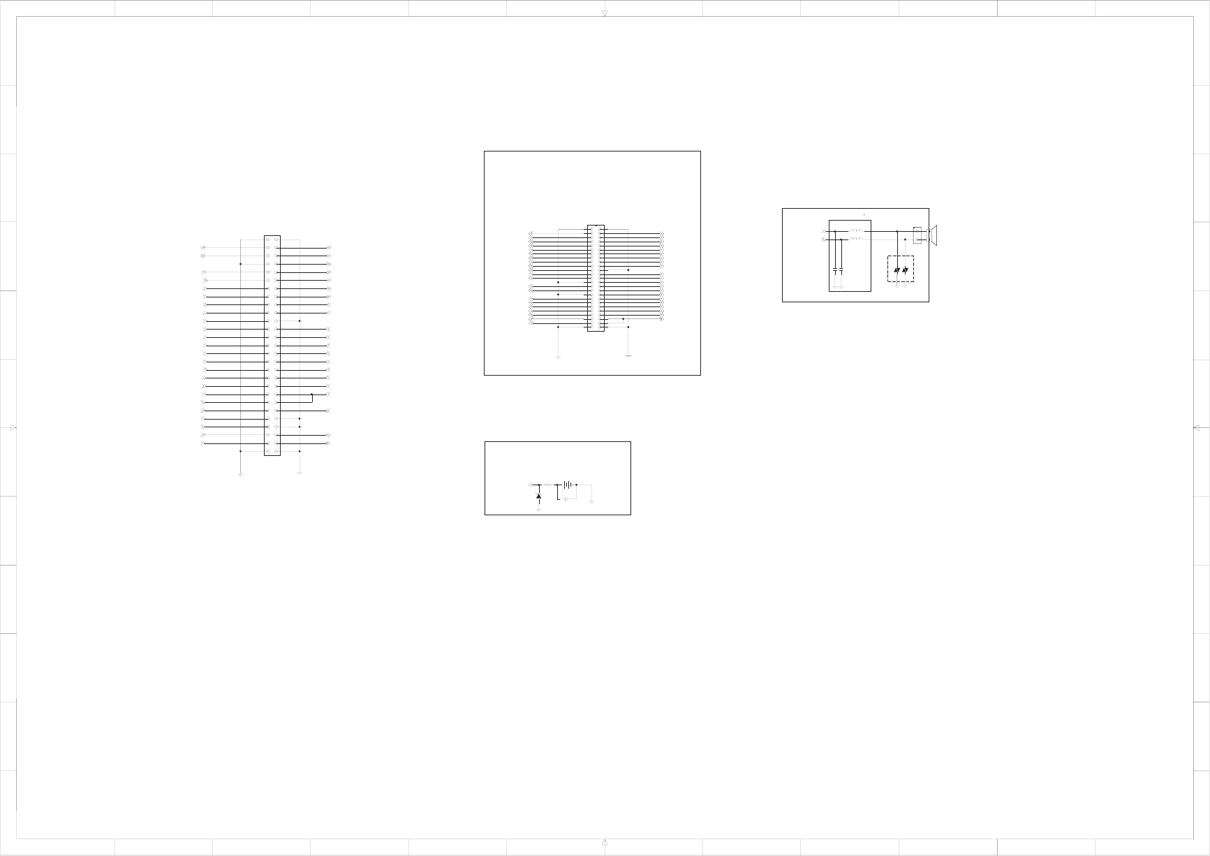
7. CIRCUIT DIAGRAM
- 134 -
LGE Internal Use Only Copyright © 2010 LG Electronics. Inc. All right reserved.
Only for training and service purposes
2.2uC103
R101
4.7K
M101
L
K
J
I
H
G
F
E
D
C
B
A
12 11 10 98 7 6 5 4 3 2 1
L
K
J
I
H
G
F
E
D
C
B
A
12 11 10 98 7 6 5 4 3 2 1
CN102
2625
2724
2823
2922
3021
3120
3219
3318
3417
3516
3615
3714
3813
3912
4011
4110
429
438
447
456
465
474
483
492
501
CN103
2827
2926
3025
3124
3223
3322
3421
3520
3619
3718
3817
3916
4015
4114
42
13
4312
4411
4510
469
478
487
496
505
514
523
532
541 FB102 100n
101AV
ZD101
201C Fp93
101C Fp93
CN101
2
1
201AV
FB101 100n
GND
KEY_ROW2
KEY_ROW2
KEY_ROW1
KEY_ROW1
KEY_ROW0
KEY_ROW0
LCD_MAKER_ID
LCD_MAKER_IDRCV_N
RCV_N
RCV_P
RCV_P
LCD_RD
LCD_RD
WLED3
WLED3
WLED2
WLED2
WLED1
WLED1
KEY_COL5
KEY_COL5
LCD_VSYNC_OUT
LCD_VSYNC_OUT
LCD_RS
LCD_RS
KEY_COL6
KEY_COL6
KEY_ROW3
KEY_ROW3
KEY_COL7
KEY_COL7
VCOIN
VCOIN
LCD_DATA[7]
LCD_DATA[7]
LCD_DATA[6]
LCD_DATA[6]
LCD_DATA[5]
LCD_DATA[5]
LCD_DATA[4]
LCD_DATA[4]
LCD_DATA[3]
LCD_DATA[3]
LCD_DATA[2]
LCD_DATA[2]
LCD_DATA[1]
LCD_DATA[1]
LCD_DATA[0]
LCD_DATA[0]
LCD_WR_N
LCD_WR_N
LCD_CS_N
LCD_CS_N
LCD_RST_N
LCD_RST_N
LCD_IF_MODE[0]
LCD_IF_MODE[0]
LCD_IF_MODE[1]
LCD_IF_MODE[1]
PM_ONSW_N
PM_ONSW_N
WLED_VOUT
WLED_VOUT
SLIDE_KEY_LED
SLIDE_KEY_LED
WLED5
WLED5
WLED4
WLED4
LCD_DATA[15]
LCD_DATA[15]
LCD_DATA[14]
LCD_DATA[14]
LCD_DATA[13]
LCD_DATA[13]
LCD_DATA[12]
LCD_DATA[12]
LCD_DATA[11]
LCD_DATA[11]
LCD_DATA[10]
LCD_DATA[10]
LCD_DATA[9]
LCD_DATA[9]
LCD_DATA[8]
LCD_DATA[8]
VLDO_LCD_2V8
VLDO_LCD_2V8
VLDO_LCD_1V8
VLDO_LCD_1V8
BACKUP BAT.(SUPER CAP.)
ENBY0040401 (50Pin)
(54Pin)
Slide FPCB to Main PCB Slide FPCB to KEY PCB(Slide)
SLIDE FPCB
MAIN RECEIVER
Can be Changed to TVS or ECLAMP
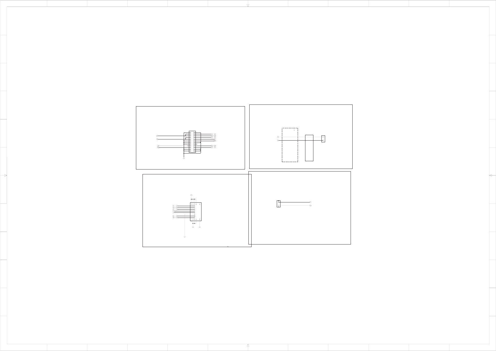
- 135 -
7. CIRCUIT DIAGRAM
LGE Internal Use OnlyCopyright © 2010 LG Electronics. Inc. All right reserved.
Only for training and service purposes
2
1
CN102
CN101
1110
129
138
147
156
165
174
183
192
201
G1 G2
G3 G4
VB101
2
1
S101
16
8
7
6
5
4
3
2
1 15
G5 G3 G1 CD
C1
C2
C3
C4
C5
C6
C7
C8
G6 G4 G2 COM
G7
L
K
J
I
H
G
F
E
D
C
B
A
12 11 10 98 7 6 5 4 3 2 1
L
K
J
I
H
G
F
E
D
C
B
A
12 11 10 98 7 6 5 4 3 2 1
MOTOR_POWER_N
MOTOR_POWER_N
SPK_OUT_P
SPK_OUT_P
SPK_OUT_N
SPK_OUT_N
MSD_D[3]
MSD_D[3]
MSD_D[2]
MSD_D[2]
MSD_D[1]
MSD_D[1]
MSD_CMD
MSD_CMD
VBAT
VBAT
MSD_D[0]
MSD_D[0]
MSD_CLK
MSD_CLK
VREG_MICROSD_3V0
VREG_MICROSD_3V0
Can be Changed to TVS or ECLAMP
SPK Common Circuit
From Module FPCB to Main PCB Connector BUSEON 16pi 3.0t 0.8W
VIBRATOR
NORMAL TYPE
PUSH PUSH 1.32t
MICRO SD
MODULE FPCB
ELCO8000_0610 Update
LG Innoteck/ Sodering 17mm
- 136 -
LGE Internal Use Only Copyright © 2010 LG Electronics. Inc. All right reserved.
Only for training and service purposes
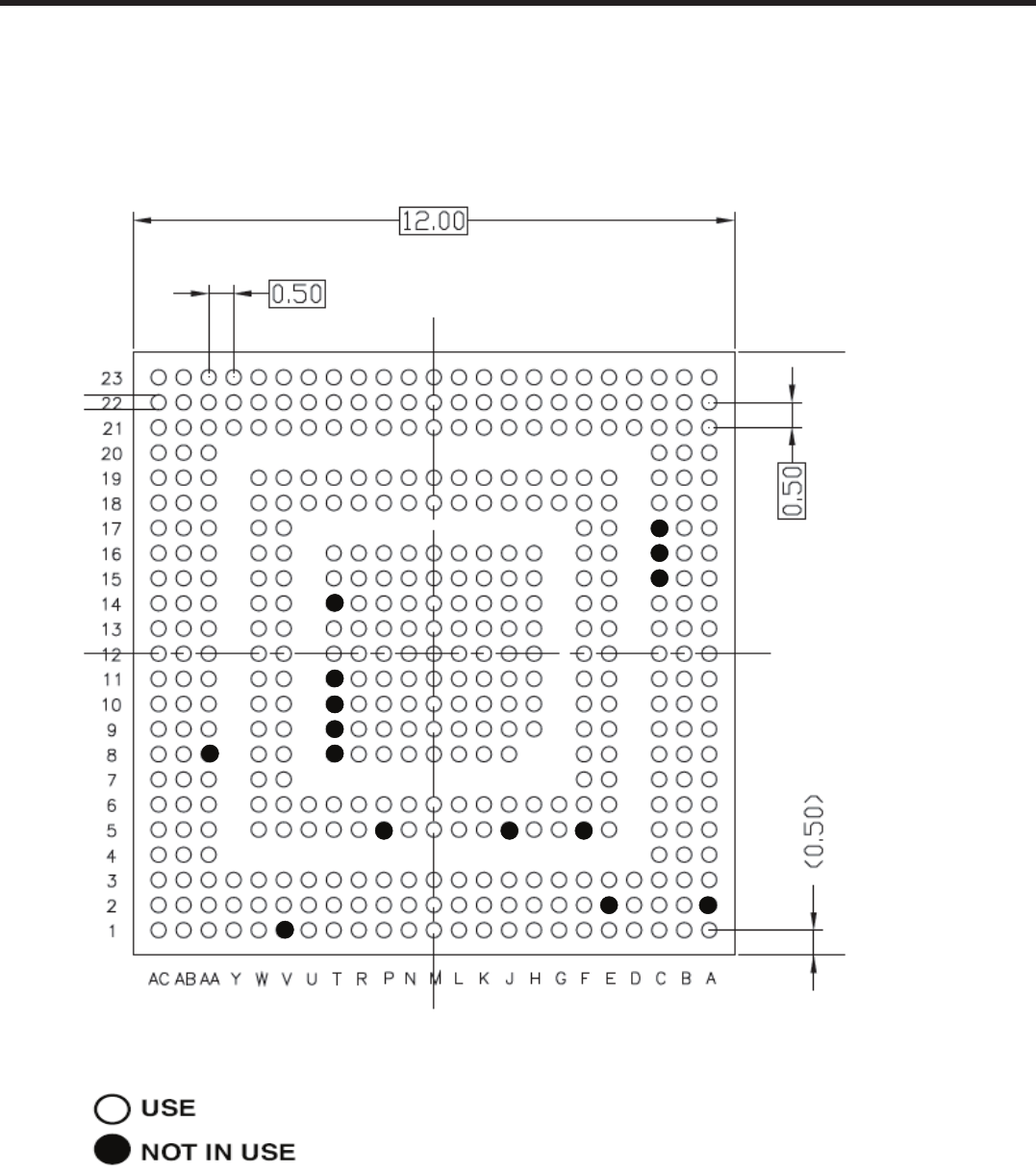
- 137 -
Copyright © 2010 LG Electronics. Inc. All right reserved.
Only for training and service purposes
LGE Internal Use Only
8. BGA PIN MAP
8. BGA PIN MAP
1. BGA PIN MAP
QSC6270 3G disableٛ- U200 (bottom view)
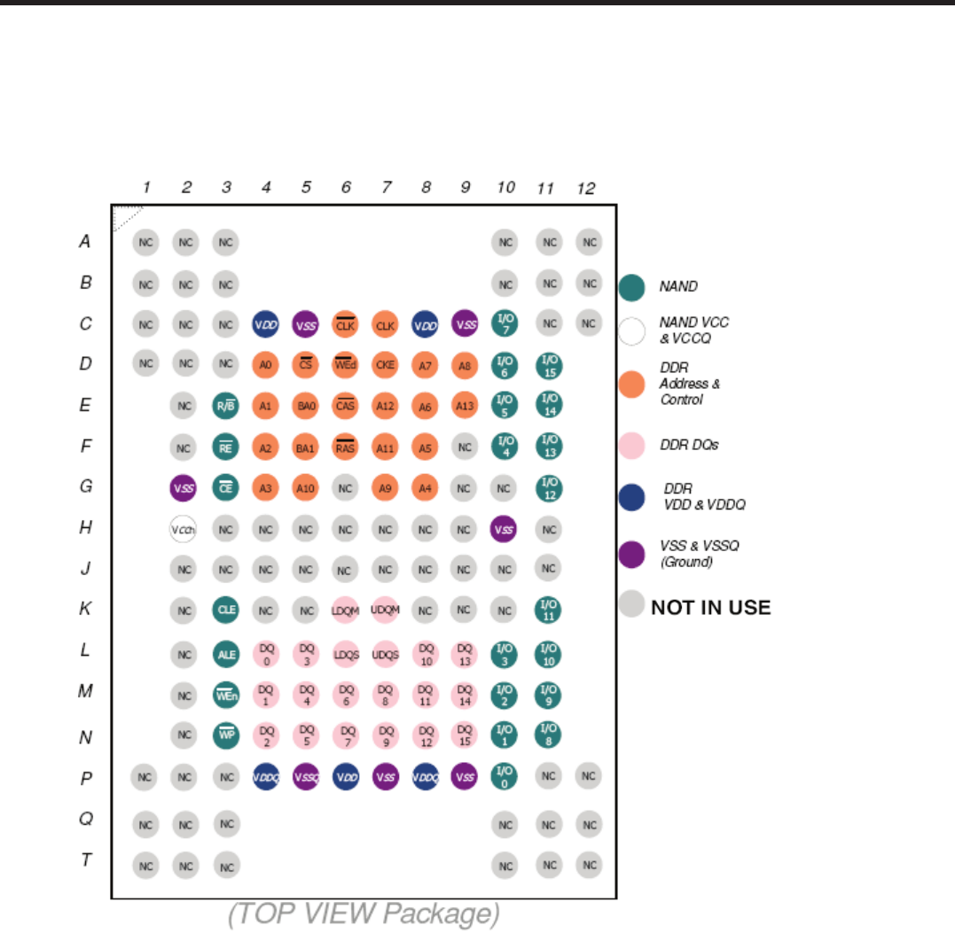
- 138 -
LGE Internal Use Only Copyright © 2010 LG Electronics. Inc. All right reserved.
Only for training and service purposes
8. BGA PIN MAP
H8BCS0SI0BAR-46M (MCP,NAND) – U300 (EUSY0347506)
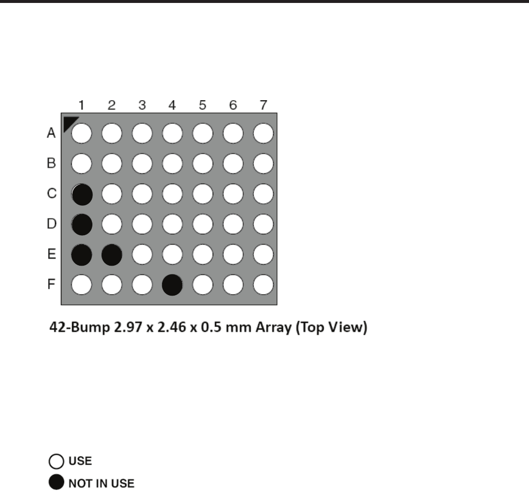
- 139 -
Copyright © 2010 LG Electronics. Inc. All right reserved.
Only for training and service purposes
LGE Internal Use Only
8. BGA PIN MAP
BCM2070B2KUBXG (bluetooth) – U700 (EUSY0418701)
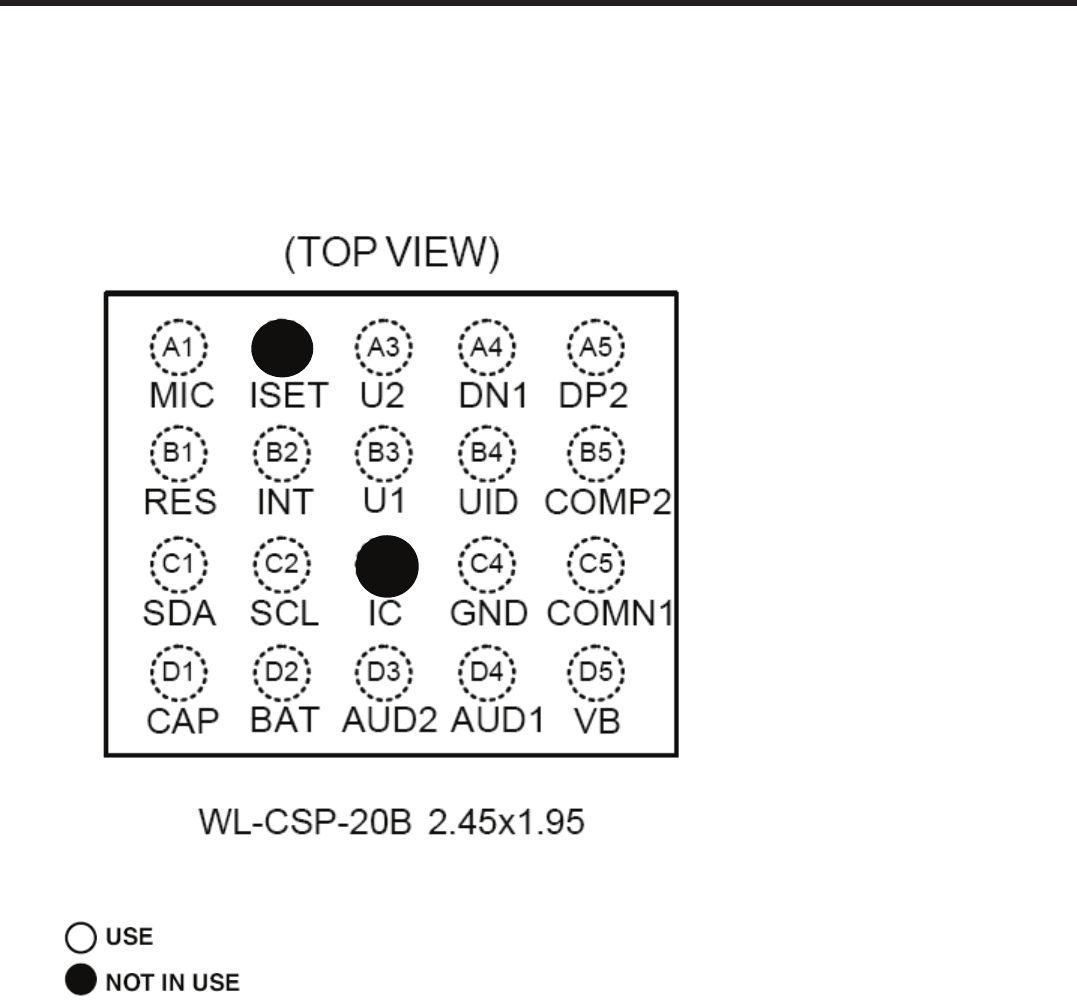
- 140 -
LGE Internal Use Only Copyright © 2010 LG Electronics. Inc. All right reserved.
Only for training and service purposes
RT8963WSC (Multiplexer Mini/Micro USB Interface)– IC400 (EUSY0424801)
8. BGA PIN MAP
- 141 -
Copyright © 2010 LG Electronics. Inc. All right reserved.
Only for training and service purposes
LGE Internal Use Only
8. BGA PIN MAP
WM9093 (Ultra Low Power Audio Subsystem)– IC500 (EUSY0403901)
20-bump CSP package; Top View
- 142 -
LGE Internal Use Only Copyright © 2010 LG Electronics. Inc. All right reserved.
Only for training and service purposes
8. BGA PIN MAP
TEA5991(FM Tuner)– U701 (EUSY0385901)
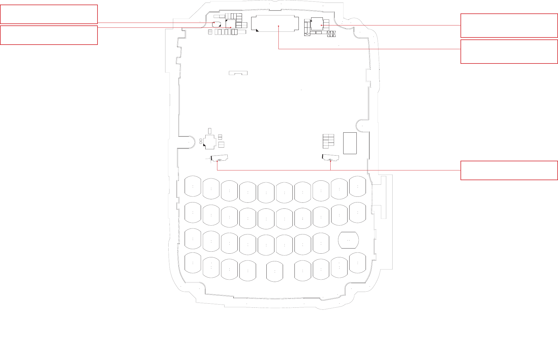
- 143 -
9. PCB LAYOUT
LGE Internal Use OnlyCopyright © 2010 LG Electronics. Inc. All right reserved.
Only for training and service purposes
28
27
54
51
D
6 0
1
51
KB809
KB836
KB811
KB820
KB818
KB837
516
C
C613
C609
806
C
R603
VA802
VA804
KB808
KB819
KB828
KB833
CN801
C510
C511
605R 805C
KB803
KB831
IC501
KB802
KB813
KB812
KB822
KB823
KB832
2
0
8
NC
KB829
VA803
C805
LD801
R271
C614
R604
R270
31
8
R
01
8
R
11
8
R
C803 C804
R806
R802
R805
C611 C612
U601
016
C
83
8BK
706
C
KB807
KB817
KB826
6
18
B
K
KB806
KB827
KB805
KB815
KB825
9
38
BK
KB804
KB814
KB824
KB834
61
5C
8
1
5C
FB502
3
05C
4
0
5
C
FB506
FB508
C524
FB507
C517
4
1
5
C
C515
R507
905C
60
5C
7
0
5
C
325C
LD802
1
0
8
U
C268
C269
R801
VA801
0
62
NC
C801
C802
TP202
662
AV
TP201
KB801
KB810
KB821
KB830
C320_MAIN_SPFY0235601_1.1_TOP
LD801/802 Main Key LED
- Can not use LED
U801 Hall IC
- Can not use Slide Detection
IC501 Audio Sub System
- Can not use Sound,Headset
U601 Charge Pump+Dual LDO
- Can not use LCD Display,
LCD Backlight, Slide Detection
CN801 FPCB Conn
- Can not use LCD, Receiver,Sub Key,
Sub key LEDs, Vibrator, Power On
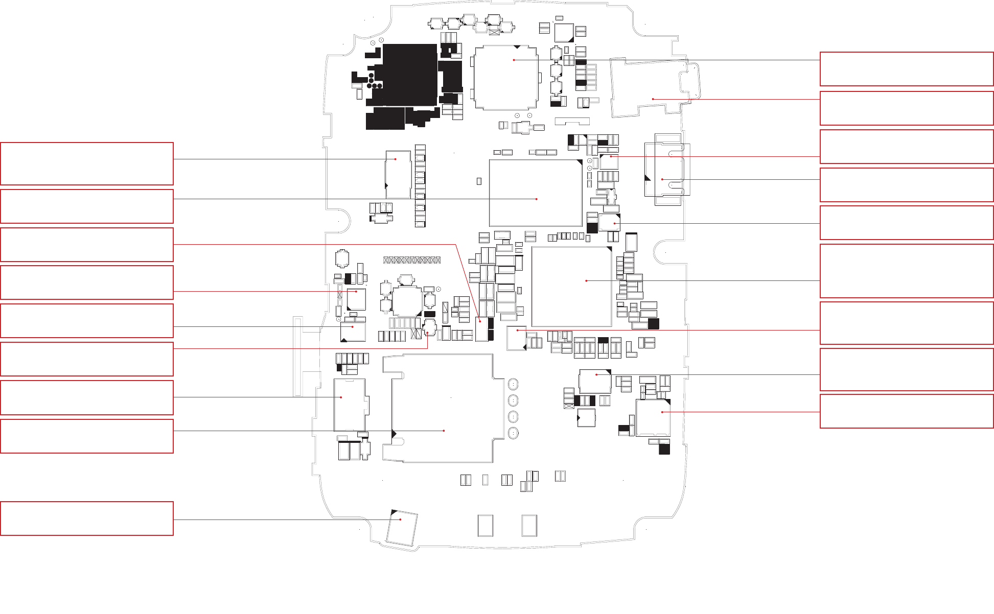
9. PCB LAYOUT
- 144 -
LGE Internal Use Only Copyright © 2010 LG Electronics. Inc. All right reserved.
Only for training and service purposes
B
01
D
F
A
1
7
F
E
D
C
1102
T
K
L
M
N
P
Q
E
F
G
H
J
6
BA
CA
AA
Y
W
V
U
T
A
B
C
21
B
F
E
D
C
1A
1
H
G
N
P
M
L
K
J
R
B
A
15
C
D
A
B
C
D
E
132
U201
5
37
C
R403
2
0
4N
C
TP701
FB702
1
0
7
L
D201
C725
X702
4
03C
C740
36
2
A
V
R404
U702
8
1
7
C
407
R
727C
01
7R
U802
90
5AV
708C
J301
FL803
50
6
C
C246
C311
L202
C243
C262
C261
C240
10
2
TP 901
C
U701
C709
106
P
T
C309
70
3
C
R272
R273
142
C
C203
01
1
C
ANT102
R505
R405
C137
VA502
FB504
R504
FB505
FB503
8
07
PT
C502
99
2C
C501
01
3
C 803C
9
07
PT
R406
R407
C410
C219
C213
C214
C212
C220
C236
C239
C232
C238
3
0
1
L
C107
FL101
3
11R
SW101
L109
J501
CN403
C233
C227
C117
C121
C120
C119
C724
637C
307
BF
10
4
AV
10
7L
F
C722
6
2
7C
3
2
7C
2
0
7
R
TP710
46
2
A
V
6
1
4C
562A
V
5
14C
C413
TP702
2
17
C
C716
0
2
7
C
C713
C710
3
07L
TP707 TP705TP706
TP703
TP704
C742
307
C
C717
C704
50
7C
9
1
7C
1
0
2
A
V
4
0
2C
12
7
C
307
R
3
0
7U
C739
0
6
2
A
V
1
6
2
A
V
262A
V
4
14C
2
0
4
D
Z
C417
FL808
2
0
7L
308NC
70
6D
Z
606DZ
2
17
R
7
0
7
R
1
1
7R
60
7R
507
R
6
08
LF
70
8L
F
70
8
R
1
0
3R
608C
103C
203C
8
42C
908
R
30
3C
MIC501
C247
R307
FL805
237
C
9
2
7C 8
27
C
037C
13
7
C
3
3
7C
L810
L811
ZD311
R308
C312
ZD310
ZD308
R309
R310
R311
ZD306
ZD307
ZD305
3
1
7
R
9
0
7R
8
07
R
517R
417
R
9
08LF
TP802
R808
382R
4
8
2R
308
U
R1
672
C
1
07
X
4
06
A
V
C224
FL804
808
A
V
018
AV
908
A
V
C714
R602
3
0
6
C
C715
FB701
406
C
U704
C741 C737
837
C
VA602
VA603
VA601 R268
R269
C223
418R
R205
362R
C207
6
25C
C211
8
0
5A
V
C210
525C
9
82
C
C209
3
0
8L
4
0
8
L
5
2
2C
4
42C
1
0
2C
7
5
2C
C249
FL811
FL802
R803
C305
4
3
7
C
R281
R282
9
5
2C
5
0
2C
C250
702
R
8
5
2C
6
0
2C
10
2X
6
92C
7
92C
91
1
L
ANT101
2
02
X
TP262
511
C
FL810
S601
206
PT
60
6
C
1
0
5Q
01
5
R
R302
R262
C245
C208
L208
C255
2
02D
C254
L203
C256
352C
L201
C252
C298
TP260
TP263
TP264
608L
50
8L
106
LF
C601
U301
102R
2
0
2C
C706
C707
306L
F
2
0
6
L
F
R601
R511
R303 R304
1
2
2C
222C
572
C
152C
R260
R261
2
0
8L
7
1
1
L
VA501
4
0
5
A
V
125C
206
C
C114
0
1
1
R
111R
211C
C134
VA505
C708
1
0
7
C
VA522
762R
L501
6
6
2
R
R509
C520
VA503
R508
C519
U501
305
R
1
0
5R
FB501
6
12
C
712C
81
2
C
60
3
C
51
2C
24
2
C
662C
C113
C291
8
01L
701L
6
1
1L
C290
L1113
C135
R109
108L
1
0
4
L
F
IC401
10
4
R
C404
1
0
4
U
L118 C101
5
0
1
C
501L
111C
R502
46
2C
C265 C407
912
R
C505
3
62
C
C403
104
C
50
4
C
9
0
4
C
6
04C
C408
C402
204R
1
1
4
C
2
0
1L
10
1L
C104
401L
C102
511L
C228
81
1C
011
L
21
4C
C226
C260
R265
R264
C267
C230
C235
C234
C229
C231
L207
602
R
L206
C237
L205
L204
621C
L111
9
21C
7
0
1
R
R112
C143
R114
C123
221C
L114
1
0
4NC
C280
C281
8
21
C
7
2
1
C
401R
2
01
R
R103
1
0
1U
C130
3
3
1
C
231C
L112
C320_MAIN_SPFY0235601_1.1_BOT
U301 Memory
- Can not Boot
J501 Ear-Jack
- Can not use Ear-Mic
IC401 MUIC
- Can not use USB, UART, Headset
CN403 USB Conn
- Can not use USB
U401 Single Charger
- Can not use Charging, Booting
U201 QSC6270 (BB & Power chipset)
- Can not power on
- No LCD Display
- No Service
X202 XO
- Can not BootRF Rx/Tx
- No Power.
FL101 FEM
- GSM RX Sensitivity & TX Power
- No service
U101 GSM PAM
- Tx power No service
S601 Camera Socket
- Can not use Camera
CN803 FPCB Conn
- Can not use SD-card, Vibrator,
Speaker
X201 Sleep Cystal
- No Service
U703 BT Chip.
- Can not use BT
X702 BT X-Tal
- Can not use BT
U803 Analog Switch
- Can not use UART, BT
CN402 Battery Conn
- Can not use Battery, Power On
J301 USIM Conn.
- Can not detect USIM
MIC501 Mic.
- Can not use Mic
- 145 -
9. PCB LAYOUT
LGE Internal Use OnlyCopyright © 2010 LG Electronics. Inc. All right reserved.
Only for training and service purposes
KB103
KB102
KB105
LD104
LD105
KB108
KB109
KB110
LD108
KB101
LD106
30
1
D
L
KB104
KB111
KB106
KB107
7
0
1
D
L
C320_KEY_SPEY0068201_10_TOP
LD107/LD108/LD106/LD104/LD105/LD103
Sub Key LED
- Can not use LED
9. PCB LAYOUT
- 146 -
LGE Internal Use Only Copyright © 2010 LG Electronics. Inc. All right reserved.
Only for training and service purposes
25
2650
CN101
60
1
R
R101
R102
10
1AV
20
1AV
5
01
R
7
01
R
8
01
R
9
01
R
0
11
R
C101C102
CN102
C320_KEY_SPEY0068201_10_BOT
CN102 LCD Connector
- Can not use LCD Display, LCD Backlight
CN101 FPCB Connector
- Can not use LCD, Sub key Operation,
Sub Key LED, Receiver
- 147 -
9. PCB LAYOUT
LGE Internal Use OnlyCopyright © 2010 LG Electronics. Inc. All right reserved.
Only for training and service purposes
C320_F_SLIDE_SPCY0246901_10_TOP
26
25
50
27
28 54
CN102
CN103
101
N
C
FB101
VA101
VA102
FB102
1
01R
301C
10
1DZ
M101
1
01C201C
CN102 FPCB Conn
- Can not use LCD, Sub key Operation,
Sub Key LED, Receiver
CN103 FPCB Connector
- Can not use LCD, Sub key Operation,
Sub Key LED, Receiver
9. PCB LAYOUT
- 148 -
LGE Internal Use Only Copyright © 2010 LG Electronics. Inc. All right reserved.
Only for training and service purposes
11
02
0
1
1
01
S
VB101
1
01N
C
20
1
NC
C320_F_SUB_SPCY0247101_10_BOT
CN101 FPCB Conn
- Can not use SD-card, Vibrator, Speaker
S301 MicroSD Socket
- Can not use MicroSD
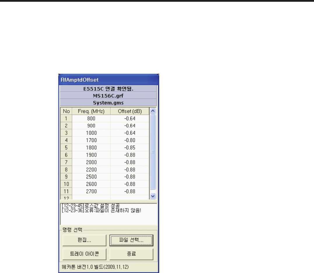
- 149 -
Copyright © 2010 LG Electronics. Inc. All right reserved.
Only for training and service purposes
LGE Internal Use Only
10. RF CALIBRATION
10. RF CALIBRATION
10.1 Usage of Tachyon for RF Calibration and Test
10.1.1 Preparation work for setting RF cable loss
Procedure
1. Click “Hecaton.exe” in below directory to set RF cable loss on test equipment.
“C:\LGE\Tachyon\Utilities”
2. After selecting “Select File” button, select right RF cable loss file corresponding to RF cable that you use.
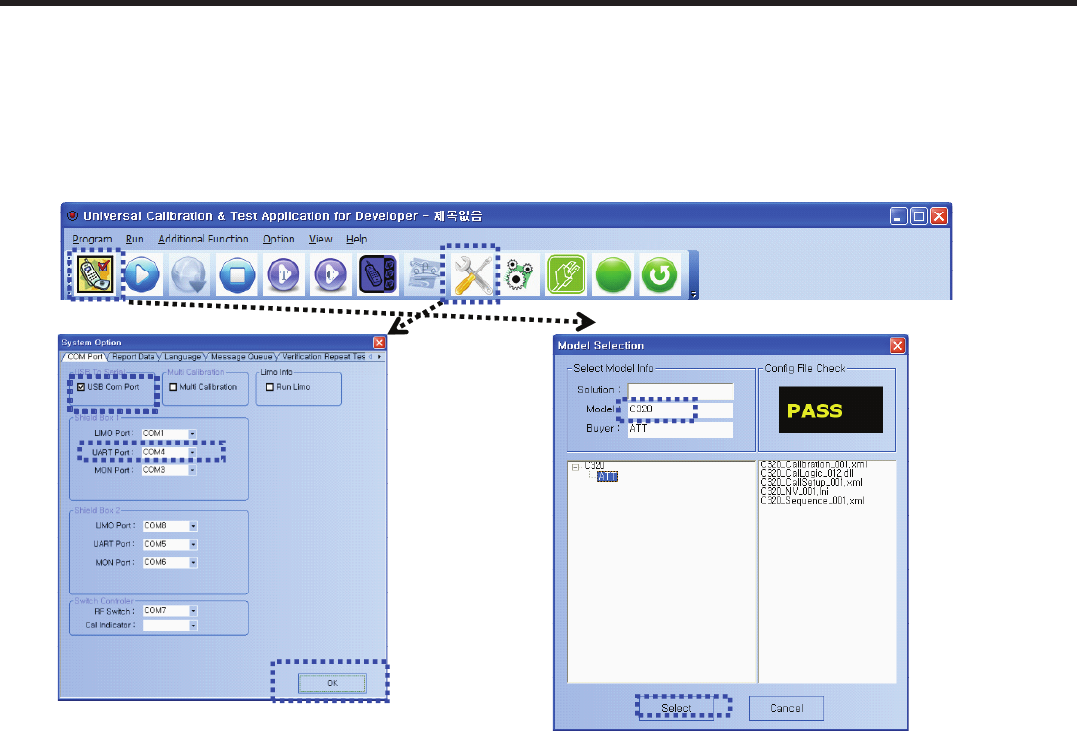
- 150 -
LGE Internal Use Only Copyright © 2010 LG Electronics. Inc. All right reserved.
Only for training and service purposes
10. RF CALIBRATION
10.1.2 Basic Setting of Tachyon for RF Calibration & Test
Procedure
1. Click “Tachyon_xxx.exe” in below directory to execute Tachyon program. “C:\LGE\Tachyon\”
2. Click “System Option Setting” icon in the menu to set COM port.
Select “UART Port” that can communicate with phone in the Shield Box 1 message.
Click the “OK” button.
3. Click “User Model Selection” icon in the menu to set model configuration.
Do double-click model/buyer name that you want to calibrate and test.
Click the “Select” button.
[ System Option Setting] [ User Model Selection]
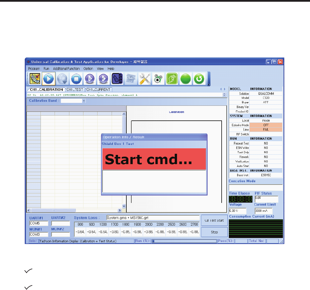
- 151 -
Copyright © 2010 LG Electronics. Inc. All right reserved.
Only for training and service purposes
LGE Internal Use Only
10. RF CALIBRATION
10.1.3 Log of RF Calibration and Test
Contents
On Running, log window is created in upper area.
It displays logs of phone commands and measurements for RF calibration and test.
The result files are saved in below directory
- “C:\LGE\Tachyon\Report\CalData\” : the file of RF calibration result
- “C:\LGE\Tachyon\Report\TestData\” : the file of RF test result
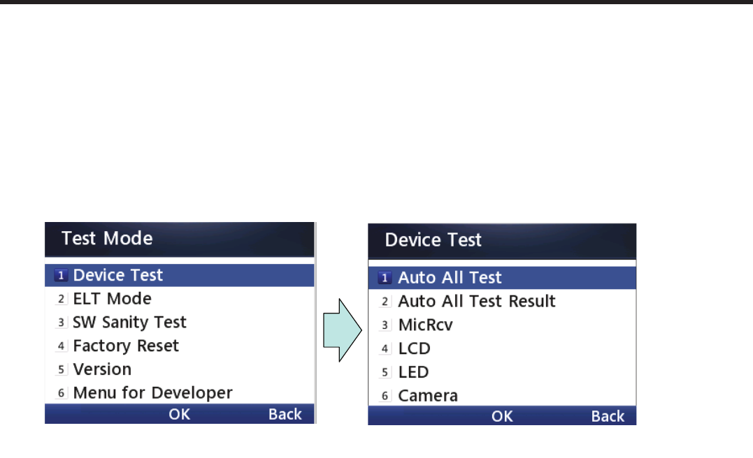
- 152 -
LGE Internal Use Only Copyright © 2010 LG Electronics. Inc. All right reserved.
Only for training and service purposes
11. TEST ALONE
Phone Test Mode : LG-C320
1. Enter the Engineer Menu
2. Tap 1. Device Test
3. Tap 1. Auto ALL Test
11.1 Phone Test Mode
11. TEST ALONE
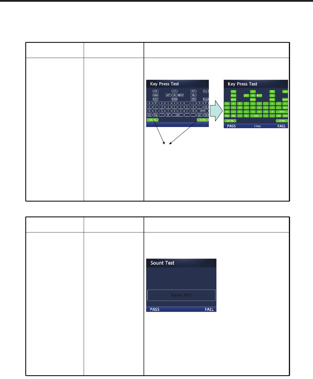
- 153 -
Copyright © 2010 LG Electronics. Inc. All right reserved.
Only for training and service purposes
LGE Internal Use Only
11. TEST ALONE
Phone Test Mode Scenario
Item Order Description
(1) Key Press, External
Memory, and SIM
card Test Start
1.Key, External Memory,
and SIM card Test
2. IF OK, tab “LSK”
Button.
It means “PASS”
Key Test
Press all keys for test
- UP key
- Down key
- Right key
- Left key
………..
…….
….
External memory and
SD card is inserted
then Sing of
“SIM Pass” and
“SD Pass” is green.
Phone Test Mode Scenario
Item Order Description
(2) Sound 1. Sound On
2. IF OK, tab “LSK”
Button.
It means “PASS”
Ringtone (MP3) is played
regularly
Press “LSK” button (Left top Key)
Move to next step
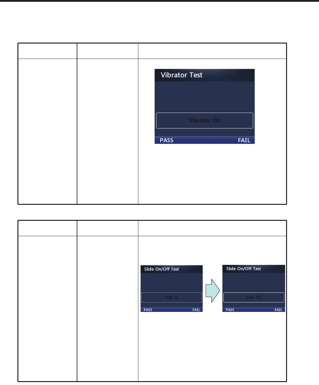
- 154 -
LGE Internal Use Only Copyright © 2010 LG Electronics. Inc. All right reserved.
Only for training and service purposes
11. TEST ALONE
wG{GtGz
Item Order Description
(3) Vibrator Test 1.Vibrator On
2. IF OK, tab “LSK”
Button.
It means “PASS”
Press “LSK” button (Left top Key)
Move to next step
wG{GtGz
Item Order Description
(4) Slide On/Off Test 1.Move Slide Up and
Down
2. IF OK, tab “LSK”
Button.
It means “PASS”
Slide UP status
Press “LSK” button (Left top Key)
Move to next step`
Slide Down status
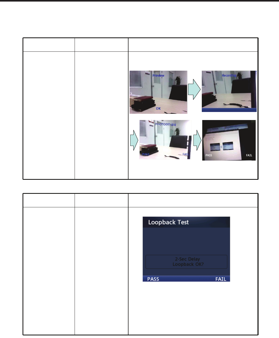
- 155 -
Copyright © 2010 LG Electronics. Inc. All right reserved.
Only for training and service purposes
LGE Internal Use Only
11. TEST ALONE
wG{GtGz
Item Order Description
(5) Camera Test 1. Camera Off
2. Camera Auto On
( Preview )
3. Photo Shot by press
“OK” key
4. Photo Save
5. Record video
6. Video Save
7. Call Photo
If OK , Press “LSK” key
(Left top Key)
8. Call Video
9. Preview
10. IF OK, tab “LSK”
Button. It means
“PASS”
wG{GtGz
Item Order Description
(6) Loopback Test 1.Loopback On
2. Speak something
3. After 2 Sec, listen the
voice
4. IF OK, tab “LSK”
Button.
It means “PASS”
5. The TEST END
Press “LSK” button (Left top Key)
TEST END

- 156 -
LGE Internal Use Only Copyright © 2010 LG Electronics. Inc. All right reserved.
Only for training and service purposes
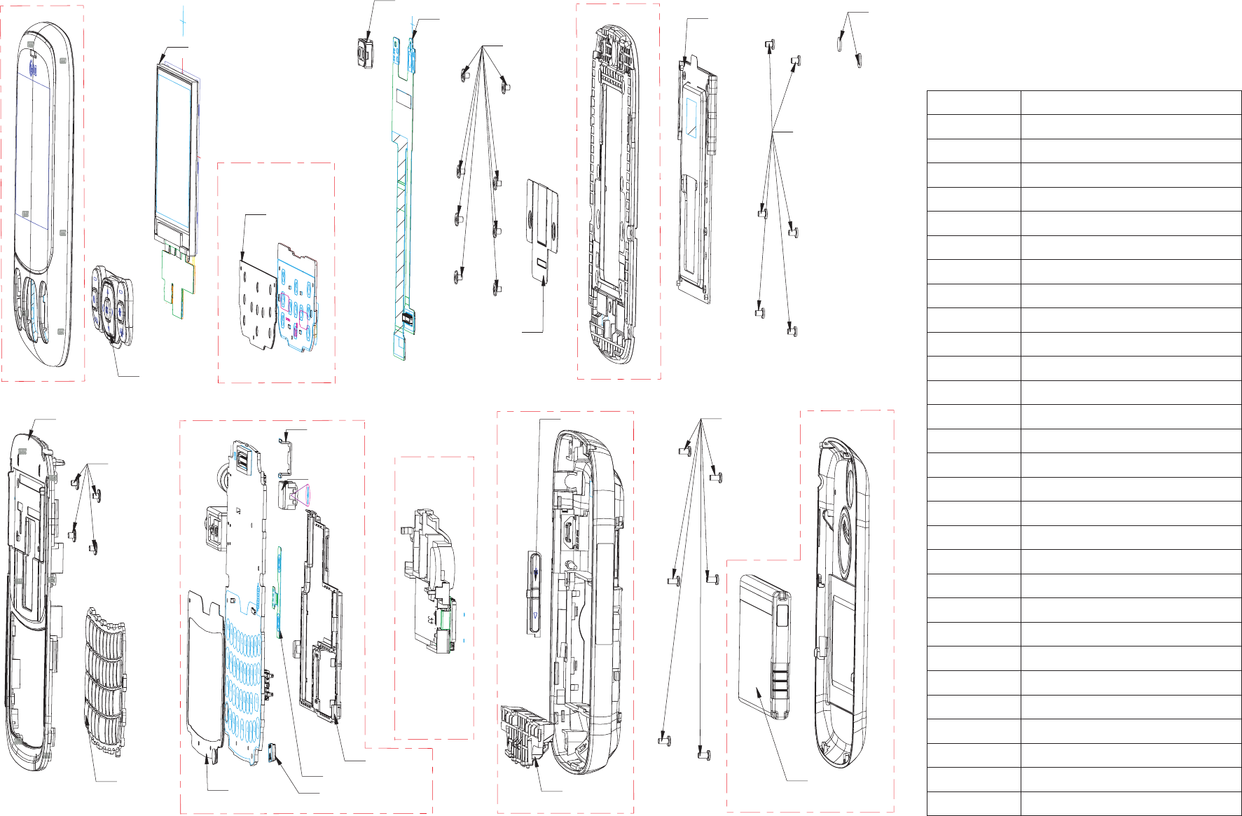
- 157 -
12. EXPLODED VIEW & REPLACEMENT PART LIST
12.1 EXPLODED VIEW
LGE Internal Use OnlyCopyright © 2010 LG Electronics. Inc. All right reserved.
Only for training and service purposes
ACGT00
SVLM00
SAEY00
ABGZ01
ACGK00
GMEY01
SAFY00
SVCY00
MCBA01
ABFZ00
ACGM00
MBJZ00 GMEY00
ACGA00
SNGF00 SBPL00
ABGZ00 ADCA00 SUMY00
SPKY00
MCBA00
ADCA01
ABFZ01
SURY00
SACY00
GMEY01
ACGU00
AHFY00 MCCH00
GMEY02
Location
ACGA00
SBPL00
ABFZ00
ACGM00
SNGF00
MBJZ00
GMEY00
ABGZ00
ABGZ01
ACGT00
AHFY00
SURY00
ABFZ01
ACGK00
ACGU00
GMEY01
GMEY02
MCCH00
SACY00
SAEY00
ADCA01
SVLM00
SAFY00
SVCY00
SPKY00
MCBA00
ADCA00
MCBA01
SUMY00
Description
Cover Assembly,Battery
Mobile Phone Battery Li-Ion
Bracket Assembly
Cover Assembly,Rear
Antenna,Helical
Button
Screw,Machine
Button Assembly
Button Assembly
Cover Assembly,Upper
HINGE ASSY
Receiver
BRACKET ASSY
Cover Assembly,Front
Cover Assembly,Lower
Screw,Machine
Screw,Machine
Cap,Screw
PCB Assembly,Flexible
PCB Assembly,Keypad
Dome Assembly,Metal
LCD,Module-TFT
PCB Assembly,Main
Camera Module
PCB,Sidekey
Can,Shield
Dome Assembly,Metal
Can,Shield
Microphone,Condenser
- 158 -
LGE Internal Use Only Copyright © 2010 LG Electronics. Inc. All right reserved.
Only for training and service purposes
- 159 -
Copyright © 2010 LG Electronics. Inc. All right reserved.
Only for training and service purposes
LGE Internal Use Only
12. EXPLODED VIEW & REPLACEMENT PART LIST
by SBOM standard on GCSC
Level LocationNo. Description PartNumber Spec Remark
1 AAD000000 Addition Assembly - AAAY0524401 LG-C320 BOOWA ZZ:Without Color -
2 ACGA00 Cover Assembly,Battery - ACGA0048201 LG-C320i IDNWA WA:White -
3 MCJA00 Cover,Battery MCJA0120401 COMPLEX LG-C320i IDNWA ZZ:Without Color COMPLEX,(empty),
3 MPBN00 Damper,Speaker MPBN0093201 COMPLEX LG-C320i IDNWA WA:White COMPLEX, (empty), , , , ,
2 MFL053800 Manual,Operation MFL67003501 COMPLEX LGC320.ABOOWA ZZ:Without Color LGC320 manual for
BOO
1 AGF000000 Package Assembly - AGF75960001 LGC320.ABOOWA ZZ:Without Color LGC320 BOO(TR3/STD
UB/1160*1160 Pallet/600ea)
2 MAY084000 Box,Unit MAY64811601 COMPLEX LGC320.ABOOWA ZZ:Without Color LGC320 BOO(TR3
STD UB)
2 MAF086500 BAG,VINYL(PE) MBAD0005204 LG-LX260 SPRAG AG,ZZ,COMPLEX, (empty), , , , ,
2 AGJ000000 PALLET ASSY - APLY0002405 KP110 OPTBK BK,ZZ,TR3 Australia(600ea) Pallet Assy
3 MBEC00 BOX,CARTON MBEC0002002 KG270 CIS BK,ZZ,BOX, TW
3 MCCL00 Cap,Box MCCL0000402 COMPLEX KG270 CIS ZZ:Without Color BOX,TW, PBO PBOTW
3 MPCY00 Pallet MPCY0015703 COMPLEX TU500 TELBK SV:Silver
COMPLEX,(empty),1160,1160,126,
3 MSCA00 SLEEVE,BOX MSCA0000701 MG230d CLA TS,ZZ,BOX, TW
2 MAY047100 Box,Master MBEE0059803 COMPLEX KP100 GBRLA ZZ:Without Color -
2 MEZ003500 Label,Barcode MLAC0004541 COMPLEX HB620 KPNBK ZZ:Without Color -
2 MEZ047200 LABEL,MASTER BOX MLAJ0004402 CG300 CGR DG,ZZ,LABEL,MASTER BOX(for CGR TDR 2VER.
mbox_label)
2 MEZ000000 LABEL MLAZ0050901 KU990 GBRBK BK,ZZ,PRINTING, (empty), , , , ,
1 APEY00 PHONE - APEY0988401 LG-C320 BOOWA WA,ZZ,
2 MEZ002100 Label,Approval MLAA0062311 COMPLEX KB770 DEUBK ZZ:Without Color -
2 ACGY00 COVER ASSY,EMS - ACGY0088801 LG-C320 BOOWA WA,ZZ,
3 ABFZ00 Bracket Assembly - ABFZ0028101 LG-C320 BOOWA ZZ:Without Color -
4 MEV000000 Insulator MIDZ0281601 COMPLEX LG-C320i IDNWA ZZ:Without Color COMPLEX, (empty), ,
, , ,
4 MCQ049800 Damper,Motor MPBJ0079001 COMPLEX LG-C320i IDNWA WA:White COMPLEX, (empty), , , , ,
4 MJN000000 Tape MTAZ0358201 COMPLEX LG-C320i IDNWA WA:White COMPLEX, (empty), , , , ,
4 MCQ015700 Damper,Connector MPBU0114101 COMPLEX LG-C320i IDNWA WA:White COMPLEX, (empty), , , , ,
12.2 Replacement Parts Note: This Chapter is used for reference, Part order is ordered
<Mechanic component>
- 160 -
LGE Internal Use Only Copyright © 2010 LG Electronics. Inc. All right reserved.
Only for training and service purposes
12. EXPLODED VIEW & REPLACEMENT PART LIST
Level LocationNo. Description PartNumber Spec Remark
3 ACGM00 Cover Assembly,Rear - ACGM0168401 LG-C320i IDNWA ZZ:Without Color -
4 MJN061100 Tape,Protect MJN67687301 COMPLEX LGC320I.AIDNWA GN:Green -
4 MBJZ00 Button MBJZ0041901 COMPLEX LG-C320i IDNWA ZZ:Without Color COMPLEX,(empty),
4 MCCE00 Cap,Receptacle MCCE0061601 COMPLEX LG-C320i IDNWA ZZ:Without Color COMPLEX,(empty),
4 MCJN00 Cover,Rear MCJN0127401 COMPLEX LG-C320i IDNWA ZZ:Without Color COMPLEX,(empty),
4 MDAY00 Decor MDAY0086001 COMPLEX LG-C320i IDNWA ZZ:Without Color COMPLEX,(empty),
4 MLAB LABEL,A/S MLAB0001102 C2000 CGRSV SV,WA,C2000 USASV DIA 4.0
4 MPBJ00 Damper,Motor MPBJ0078101 COMPLEX LG-C320i IDNWA ZZ:Without Color COMPLEX,(empty),
4 MPBN00 Damper,Speaker MPBN0091501 COMPLEX LG-C320i IDNWA ZZ:Without Color COMPLEX,(empty),
4 MPBT00 Damper,Camera MPBT0098901 COMPLEX LG-C320i IDNWA ZZ:Without Color COMPLEX,(empty),
4 MPBZ00 Damper MPBZ0337301 COMPLEX LG-C320i IDNWA WA:White COMPLEX, (empty), , , , ,
4 MTAK00 Tape,Camera MTAK0041901 COMPLEX LG-C320i IDNWA ZZ:Without Color COMPLEX,(empty),
4 MWAE00 Window,Camera MWAE0065101 COMPLEX LG-C320i IDNWA ZZ:Without Color COMPLEX,(empty),
3 GEMY00 Screw,Machine GMEY0010601 GMEY0010601 BH + 1.4mM 2.5mM MSWR FZB N - KUMGANG
SCREW CO., LTD
3 ACGQ00 Cover Assembly,Slide - ACGQ0056601 LG-C320 BOOWA WA:White -
4 ABGZ00 Button Assembly ABGZ0006901 LG-C320i IDNWA ZZ:Without Color MAIN
4 ABGZ01 Button Assembly ABGZ0007001 LG-C320i IDNWA ZZ:Without Color SUB
4 ACGT00 Cover Assembly,Upper - ACGT0009101 LG-C320i IDNWA ZZ:Without Color LG-C320i IDNWA
5 AJX00 Window Assembly,LCD - AJX73205001 LGC320.ABOOWA ZZ:Without Color -
6 MKC043300 Window,LCD MWAC0151901 COMPLEX LG-C320i IDNWA ZZ:Without Color COMPLEX,(empty),
5 MCJX00 Cover,Upper - MCJX0011301 COMPLEX LG-C320i IDNWA ZZ:Without Color COMPLEX,(empty),
6 MICE00 INSERT,NUT MICE0016901 MECH_COMMON ZY,ZZ,PRESS, STS, , , , ,
5 MFBZ00 Filter MFBZ0025001 COMPLEX LG-C320i IDNWA ZZ:Without Color COMPLEX,(empty),
5 MPBG00 Damper,LCD MPBG0113001 COMPLEX LG-C320i IDNWA ZZ:Without Color COMPLEX,(empty),
5 MTAD00 Tape,Window MTAD0133501 COMPLEX LG-C320i IDNWA ZZ:Without Color COMPLEX,(empty),
5 MTAZ TAPE MTAZ0113701 LG-KV5900 BK,ZZ,20X7
4 MJN061101 Tape,Protect MTAB0440401 COMPLEX LG-C320i IDNWA ZZ:Without Color COMPLEX, (empty), ,
, , ,
4 MJN061100 Tape,Protect MTAB0423001 COMPLEX LG-C320i IDNWA ZZ:Without Color -
4 MJN061102 Tape,Protect MTAB0422301 COMPLEX LG-C320i IDNWA ZZ:Without Color COMPLEX,(empty),
4 AHFY00 HINGE ASSY AHFY0002101 LG-MN240 MTP LS,ZZ,Slide
- 161 -
Copyright © 2010 LG Electronics. Inc. All right reserved.
Only for training and service purposes
LGE Internal Use Only
12. EXPLODED VIEW & REPLACEMENT PART LIST
Level LocationNo. Description PartNumber Spec Remark
4 ABFZ01 BRACKET ASSY - ABFZ0023401 LG-MN240 MTP LS,ZZ,
5 MBFZ00 BRACKET MBFZ0043001 LG-MN240 MTP LS,ZZ,COMPLEX, (empty), , , , ,
5 MTAB00 TAPE,PROTECTION MTAB0381101 LG-MN240 MTP LS,ZZ,COMPLEX, (empty), , , , ,
4 ACGK00 Cover Assembly,Front - ACGK0169801 LG-C320i IDNWA ZZ:Without Color LG-C320i IDNWA
5 MCJK00 Cover,Front - MCJK0135101 COMPLEX LG-C320i IDNWA ZZ:Without Color COMPLEX,(empty),
6 MICE00 INSERT,NUT MICE0016903 MECH_COMMON ZY,ZZ,PRESS, STS, , , , ,
5 MPBZ01 Damper MPBZ0320601 COMPLEX LG-C320i IDNWA ZZ:Without Color COMPLEX,(empty),
5 MPBZ00 Damper MPBZ0320801 COMPLEX LG-C320i IDNWA ZZ:Without Color COMPLEX,(empty),
5 MPBZ02 Damper MPBZ0366401 COMPLEX LG-C320i IDNWA ZZ:Without Color COMPLEX,(empty),
4 ACGU00 Cover Assembly,Lower - ACGU0007201 LG-C320i IDNWA ZZ:Without Color LG-C320i IDNWA
5 MCJY00 Cover,Lower MCJY0008701 COMPLEX LG-C320i IDNWA ZZ:Without Color COMPLEX,(empty),
5 MMAA00 MAGNET,SWITCH MMAA0011201 LG-LU1600 LGTWW WW,ZZ,COMPLEX, (empty), , , , ,
5 MPBZ01 PAD MPBZ0260601 LG-MN240 MTP LS,ZZ,COMPLEX, (empty), , , , ,
5 MPBZ PAD MPBZ0260901 LG-MN240 MTP LS,ZZ,COMPLEX, (empty), , , , ,
5 MPBZ02 Damper MPBZ0320401 COMPLEX LG-C320i IDNWA ZZ:Without Color COMPLEX,(empty),
4 GMEY01 Screw,Machine GMEY0017801 GMEY0017801 BH + 1.4mM 1.4mM MSWR FZB N - KUMGANG
SCREW CO., LTD
4 GMEY02 Screw,Machine GMEY0019201 GMEY0019201 FH + 1.4mM 1.8mM SWCH FZW N N KUMGANG
SCREW CO., LTD
4 MCCH00 Cap,Screw MCCH0165101 COMPLEX LG-C320i IDNWA ZZ:Without Color COMPLEX,(empty),
4 MEV000002 Insulator MEV63651701 COMPLEX LGC320.ABOOWA BL:Blue insulator, FPCB
4 MDS000000 Gasket MGAZ0112501 COMPLEX LG-C320i IDNWA ZZ:Without Color COMPLEX,(empty),
4 MEV000001 INSULATOR MIDZ0259401 LG-MN240 MTP LS,ZZ,COMPLEX, (empty), , , , ,
4 MCQ000000 Damper MPBZ0357401 COMPLEX LG-C320i IDNWA ZZ:Without Color COMPLEX, (empty), ,
, , ,
6 MJN000000 Tape MTAZ0368001 COMPLEX LG-C320i IDNWA ZZ:Without Color COMPLEX, (empty), ,
, , ,
6 MCQ015700 Damper,Connector MPBU0113901 COMPLEX LG-C320i IDNWA ZZ:Without Color COMPLEX, (empty), ,
, , ,
6 ADCA01 Dome Assembly,Metal ADCA0118401 LG-C320i IDNWA ZZ:Without Color LG-C320i IDNWA
5 MCQ000000 Damper MPBZ0349901 COMPLEX LG-C320i IDNWA ZZ:Without Color COMPLEX, (empty), ,
, , ,
5 ACKA00 Can Assembly,Shield - ACKA0035801 LG-C320i IDNWA ZZ:Without Color -
6 MCBA00 Can,Shield MCBA0086901 COMPLEX LG-C320i IDNWA ZZ:Without Color COMPLEX,(empty),
5 MEV000000 Insulator MIDZ0284101 COMPLEX LG-C320i IDNWA ZZ:Without Color COMPLEX,(empty),
- 162 -
LGE Internal Use Only Copyright © 2010 LG Electronics. Inc. All right reserved.
Only for training and service purposes
12. EXPLODED VIEW & REPLACEMENT PART LIST
Level LocationNo. Description PartNumber Spec Remark
5 ADCA00 Dome Assembly,Metal - ADCA0118501 LG-C320i IDNWA ZZ:Without Color MAIN
6 MPBZ00 PAD MPBZ0337101 LG-C320i IDNWA WA,ZZ,COMPLEX, (empty), , , , ,
5 MPBU00 Damper,Connector MPBU0113801 COMPLEX LG-C320i IDNWA ZZ:Without Color COMPLEX, (empty), ,
, , ,
5 MEZ000000 LABEL MLAZ0038301 LG-VX6000 SV,ZZ,PID Label 4 Array
6 MCBA01 Can,Shield MCBA0059201 COMPLEX GD350 CLP ZZ:Without Color -
- 163 -
Copyright © 2010 LG Electronics. Inc. All right reserved.
Only for training and service purposes
LGE Internal Use Only
12. EXPLODED VIEW & REPLACEMENT PART LIST
by SBOM standard on GCSC
Level LocationNo. Description PartNumber Spec Remark
4 EBR070500 PCB Assembly,Flexible - EBR72655001 LGC320.ABOOWA FLEXIBLE 1.0
5 EBR070400 PCB Assembly,
Flexible,SMT - EBR72681501 LGC320.ABOOWA FLEXIBLE 1.0
6 EAX010700 PCB,Flexible SPCY0247101 SPCY0247101 LG-C320i IDNWA,FLEXIBLE,E,POLYI,0.15
mm,DOUBLE SI FLEX CO., LTD
6 EBR070200 PCB Assembly,
Flexible,SMT Bottom - EBR72655201 LGC320.ABOOWA FLEXIBLE 1.0
7 CN101 Connector,BtoB ENBY0052901 55909-0274 20P 0.40MM STRAIGHT MALE SMD R/TP 1.5M -
HANKOOK MOLEX
7 S101 Socket,Card ENSY0023601 SCHA4B0402 Micro-SD 8P ANGLE SMD R/TP - ALPS ELECTRIC
KOREA CO.,LTD.
6 EBR070300 PCB Assembly,
Flexible,SMT Top EBR72681601 LGC320.ABOOWA FLEXIBLE 1.0
4 EAU010000 Motor,DC SJMY0007104 3V 80mA 0A 12KRPM 0RPM 0SEC 0GF.CM 0OHM
4 EAB010100 Speaker Module SUSY0027617 SI-C320-P LG-C320i IDNWA BUJEON ELECTRONICS CO., LTD
4 SNGF00 Antenna,Helical SNGF0064202 ACD-00094 3.0,-2 dBd,GSM Quad carrier type,QUAD,-2.0,50,3.0
MOBITECH CORPORATION
6 RAB040100 Film,Inmold BFAA0127401 BFAA0127401 ; ,BLACK , , , BLACK , , , NISSHA PRINTING CO.,
LTD
4 SURY00 Receiver SURY0010114 BWBR1207L-04B-P 30mW 32OHM 105DB 0HZTO0HZ WIRE -
BUJEON ELECTRONICS CO., LTD
4 SACY00 PCB Assembly,Flexible - SACY0127201 LG-C320 BOOWA FLEXIBLE 1.0
5 SACE00 PCB Assembly,
Flexible,SMT - SACE0114501 LG-C320 BOOWA FLEXIBLE 1.0
6 EAX010700 PCB,Flexible SPCY0246901 SPCY0246901 LG-C320i IDNWA,FLEXIBLE,D,POLYI,.12
mm,DOUBLE SI FLEX CO., LTD
6 SACC00 PCB Assembly,
Flexible,SMT Bottom SACC0085002 LG-C320 BOOWA FLEXIBLE 1.0
6 SACD00 PCB Assembly,
Flexible,SMT Top - SACD0098702 LG-C320 BOOWA FLEXIBLE 1.0
7 C101,C102 Varistor SEVY0005201 EVLC5S02050 5.5V 0% 50F 1.0*0.5*0.6 - SMD R/TP AMOTECH
CO., LTD.
7FB101,
FB102 Inductor,Multilayer,Chip ELCH0004727 1005GC2TR10J00 100NH 5% 0V 100mA 2.3OHM 600MHZ 8 NON
SHIELD 1 1.0X0.5X0.5MM R/TP PILKOR ELECTRONICS LTD.
7 CN102 Connector,BtoB ENBY0040401 GB042-50P-H10-E3000 50P 0.4MM STRAIGHT PLUG SMD R/TP
1M - LS Mtron Ltd.
7VA101,
VA102 Varistor SEVY0003901 EVL5M02200 5.5V 0% 480F 1.0*0.5*0.6 NONE SMD R/TP
AMOTECH CO., LTD.
12.2 Replacement Parts Note: This Chapter is used for reference, Part order is ordered
<Main component>
- 164 -
LGE Internal Use Only Copyright © 2010 LG Electronics. Inc. All right reserved.
Only for training and service purposes
12. EXPLODED VIEW & REPLACEMENT PART LIST
Level LocationNo. Description PartNumber Spec Remark
7 CN103 Connector,BtoB ENBY0042601 GB042-54P-H10 54P 0.40MM STRAIGHT MALE SMD R/TP 1M - LS
Mtron Ltd.
7 C103 Capacitor,Ceramic,Chip ECCH0000198 CL05A225MQ5NSNC 2.2uF 20% 6.3V X5R -55TO+85C 1005 R/TP .
SAMSUNG ELECTRO-MECHANICS CO., LTD.
7 M101 Capacitor Assembly SMZY0023501 PAS311HR-VG1 3.8 Backup Capacitor 0.03F,Module Assembly,
KOREA TAIYO YUDEN.CO., LTD.
7 ZD101 Diode,TVS EDTY0008601 PSD05-LF 5V 6 13.5V 42A 500W SOD323 R/TP 2P 1 PROTEK
DEVICES INC.
7 R101 Resistor,Chip ERHY0000254 MCR01MZP5J472 4.7KOHM 5% 1/16W 1005 R/TP - ROHM
Semiconductor KOREA CORPORATION
4 SAEY00 PCB Assembly,Keypad - SAEY0074701 LG-C320 BOOWA KEYPAD 1.0
5 EBR070900 PCB Assembly,
Keypad,Insert - EBR72665301 LGC320.ABOOWA KEYPAD 1.0
5 SAEE PCB Assembly,
Keypad,SMT - SAEE0039402 LG-C320 BOOWA KEYPAD 1.1
6 SAEC PCB Assembly,
Keypad,SMT Bottom - SAEC0038302 LG-C320 BOOWA KEYPAD 1.0
7 R101,R102 Resistor,Chip ERHZ0000434 MCR01MZP5J1R0 1OHM 5% 1/16W 1005 R/TP - ROHM
Semiconductor KOREA CORPORATION
7 C101,C102 Capacitor,Ceramic,Chip ECCH0002001 C1005JB0J104KT000F 0.1uF 10% 6.3V Y5P -30TO+85C 1005 R/TP
- TDK CORPORATION
7 CN101 Connector,BtoB ENBY0040501 GB042-50S-H10-E3000 50P 0.4MM STRAIGHT SOCKET SMD R/TP
1M - LS Mtron Ltd.
7 CN102 Connector,FFC/FPC/PIC ENQY0014901 GF032-35S-E2000 35P 0.30MM FPC STRAIGHT BOTH SMD R/TP
LOCKING - LS Mtron Ltd.
7
R105,R106,R
107,R108,R1
09,R110
Resistor,Chip ERHZ0000402 MCR01MZP5J100 10OHM 5% 1/16W 1005 R/TP - ROHM
Semiconductor KOREA CORPORATION
7VA101,
VA102 Varistor SEVY0003901 EVL5M02200 5.5V 0% 480F 1.0*0.5*0.6 NONE SMD R/TP
AMOTECH CO., LTD.
6 SAED PCB Assembly,
Keypad,SMT Top - SAED0037602 LG-C320 BOOWA KEYPAD 1.0
7
LD103,
LD104,
LD105,
LD106,
LD107,
LD108
LED,Chip EDLH0014803 SSC-WH107 WHITE 2.7~3.1 20mA 100~230mcd x, y 64mW 1608
R/TP 2P - SEOUL SEMICONDUCTOR CO.,LTD
6 SPEY00 PCB,Keypad SPEY0068201 SPEY0068201 LG-C320i IDNWA,KEYPAD,D,FR-4,.8 mm,BUILD-UP
4 UNITECH PRINTED CIRCUIT BOARD CORP.
4 SVLM00 LCD,Module-TFT SVLM0038101
DM24-DSM04
Main,2.4,320*240,54.3*46.8*1.7t,262K,TFT,TM,S6D05A0,Landscape
Type,16bit IF,For Bar Type Phone, LG Display Co. Ltd.
3 SAFY00 PCB Assembly,Main - SAFY0399101 LG-C320 MAIN 1.0
- 165 -
Copyright © 2010 LG Electronics. Inc. All right reserved.
Only for training and service purposes
LGE Internal Use Only
12. EXPLODED VIEW & REPLACEMENT PART LIST
Level LocationNo. Description PartNumber Spec Remark
4 SAFB00 PCB Assembly,
Main,Insert - SAFB0126901 LG-C320 BOOWA MAIN 1.1
5 RAA050100 RESIN,PC BRAH0001301 UF-1060,; , , , ,[empty]
5 SVCY00 Camera Module SVCY0026901 C2FK-H313A C2FK-H313A 2M FF, Hynix(1/5"), 7x7x4.1t, Socket LG
Innotek.com
5 SPKY00 PCB,Sidekey SPKY0094301 SPKY0094301 LG-C320i IDNWA,SIDEKEY,C,POLYI,0.18
mm,DOUBLE SI FLEX CO., LTD
4 SAFF00 PCB Assembly,
Main,SMT - SAFF0298001 LG-C320 MAIN 1.0
5 SAFC00 PCB Assembly,
Main,SMT Bottom - SAFC0162201 LG-C320 BOOWA MAIN 1.2
6 S601 Card Socket ENSY0022201 CAM-H88 24,ETC,mm,7*7,1.3M (1/5") Socket Type MITSUMI
ELECTRIC CO.,LTD.
6 L207 Inductor,Multilayer,Chip ELCH0004729 1005GC2T56NJ00 56NH 5% 0V 200mA 1.6OHM 900MHZ 8 NON
SHIELD 1 1.0X0.5X0.5MM R/TP PILKOR ELECTRONICS LTD.
6 C103 Capacitor,Ceramic,Chip ECCH0000198 CL05A225MQ5NSNC 2.2uF 20% 6.3V X5R -55TO+85C 1005 R/TP .
SAMSUNG ELECTRO-MECHANICS CO., LTD.
6 C735 Capacitor,Ceramic,Chip ECCH0000110 MCH155A100D 10pF 0.25PF 50V NP0 -55TO+125C 1005 R/TP -
ROHM Semiconductor KOREA CORPORATION
6 C120,C739 Capacitor,Ceramic,Chip ECCH0000112 MCH155C150J 15pF 5% 50V NP0 -55TO+125C 1005 R/TP - ROHM
Semiconductor KOREA CORPORATION
6
C301,C303,C
304,C404,C4
07
Capacitor,Ceramic,Chip ECCH0000115 MCH155A220JK 22pF 5% 50V NP0 -55TO+125C 1005 R/TP -
ROHM Semiconductor KOREA CORPORATION
6 C110 Capacitor,Ceramic,Chip ECCH0000117 CL05C270JB5NNNC 27pF 5% 50V NP0 -55TO+125C 1005 R/TP 0.5
SAMSUNG ELECTRO-MECHANICS CO., LTD.
6 C143 Capacitor,Ceramic,Chip ECCH0000195 GRM1555C1H3R9C 3.9pF 0.25PF 50V NP0 -55TO+125C 1005 R/TP
- MURATA MANUFACTURING CO.,LTD.
6 C417,C525 Capacitor,Ceramic,Chip ECCH0000120 MCH155A390J 39pF 5% 50V NP0 -55TO+125C 1005 R/TP - ROHM
Semiconductor KOREA CORPORATION
6 C708 Capacitor,Ceramic,Chip ECCH0000137 C1005X7R1H331KT000F 0.33nF 10% 50V X7R -55TO+125C 1005
R/TP - TDK KOREA COOPERATION
6VA101,
VA102 Varistor SEVY0003901 EVL5M02200 5.5V 0% 480F 1.0*0.5*0.6 NONE SMD R/TP
AMOTECH CO., LTD.
- 166 -
LGE Internal Use Only Copyright © 2010 LG Electronics. Inc. All right reserved.
Only for training and service purposes
12. EXPLODED VIEW & REPLACEMENT PART LIST
Level LocationNo. Description PartNumber Spec Remark
6
C208,C211,C
212,C213,C2
14,C215,C21
6,C217,C218
,C219,C220,
C221,C222,C
223,C229,C2
31,C235,C23
6,C305,C306
,C307,C308,
C309,C310,C
605,C606,C7
01,C709
Capacitor,Ceramic,Chip ECCH0009101 C0603X5R0J104KT00NN 0.1uF 10% 6.3V X5R -55TO+85C 0603
R/TP - TDK CORPORATION
6 C101,C102 Capacitor,Ceramic,Chip ECCH0002001 C1005JB0J104KT000F 0.1uF 10% 6.3V Y5P -30TO+85C 1005 R/TP
- TDK CORPORATION
6
C105,C117,C
118,C122,C1
30,C135,C51
9,C520,C521
Capacitor,Ceramic,Chip ECZH0000830 C1005C0G1H330JT000F 33pF 5% 50V NP0 -55TO+125C 1005
R/TP - TDK KOREA COOPERATION
6 C230,C233 Capacitor,Ceramic,Chip ECCH0006201 C1608X5R0J475KT000N 4.7uF 10% 6.3V X5R -55TO+85C 1608
R/TP - TDK CORPORATION
6
C121,C225,C
246,C252,C2
54,C255
Capacitor,Ceramic,Chip ECCH0007803 CL10A106MP8NNNC 10uF 20% 10V X5R -55TO+85C 1608 R/TP
0.8MM SAMSUNG ELECTRO-MECHANICS CO., LTD.
6
C226,C227,C
237,C244,C2
57,C258,C25
9
Capacitor,Ceramic,Chip ECCH0007802 CV105X5R475M10AT 4.7uF 20% 10V X5R -55TO+85C 1608 R/TP -
KYOCERA CORP.
6C234,C240,C
241,C243 Capacitor,Ceramic,Chip ECCH0009103 C0603C0G1H101JT00NN 100pF 5% 50V X7R -55TO+125C 0603
R/TP - TDK CORPORATION
6
C242,C253,C
256,C298,C7
21,C725,C72
6
Capacitor,Ceramic,Chip ECCH0009106 C0603X7R1C103KT 10nF 10% 10V X7R -55TO+125C 0603 R/TP -
TDK CORPORATION
6 C127 Capacitor,Ceramic,Chip ECCH0009110 C0603X7R0J223KT 22nF 10% 6.3V X7R -55TO+125C 0603 R/TP -
TDK CORPORATION
6 C129 Capacitor,Ceramic,Chip ECCH0009226 GRM0335C1E390J 39pF 5% 25V X7R -55TO+125C 0603 R/TP -
MURATA MANUFACTURING CO.,LTD.
6 C128 Capacitor,Ceramic,Chip ECCH0009228 GRM033R61A472K 4700pF 10% 25V X5R -55TO+85C 0603 R/TP -
MURATA MANUFACTURING CO.,LTD.
6 C722,C723 Capacitor,Ceramic,Chip ECCH0009514 MCH032A(AN)100DK 10pF 0.5PF 25V X7R -55TO+125C 0603 R/TP
- ROHM.
6 C602,C603 Capacitor,Ceramic,Chip ECCH0010501 GRM1555C1H7R5D 7.5pF C0G TYPE(No X7R) MURATA
MANUFACTURING CO.,LTD.
6C412,C414,C
415 Capacitor,TA,Conformal ECTH0002002
F981A336MSA 33F 20% 10V 3.3A -55TO+85C 6OHM
2.2X1.1X1.1MM - SMD R/TP NICHICON CORPORATION, EAST
JAPAN SALES OFFICE
- 167 -
Copyright © 2010 LG Electronics. Inc. All right reserved.
Only for training and service purposes
LGE Internal Use Only
12. EXPLODED VIEW & REPLACEMENT PART LIST
Level LocationNo. Description PartNumber Spec Remark
6 C526 Capacitor,TA,Conformal ECTH0004807 TCM1A106M8R 10F 20% 10V 500mA -55TO+85C 15OHM - - SMD
R/TP ROHM.
6 C113 Capacitor,Ceramic,Chip ECZH0000802 C1005C0G1H010CT 1pF 0.25PF 50V NP0 -55TO+125C 1005 R/TP -
TDK KOREA COOPERATION
6C232,C260,C
267 Capacitor,Ceramic,Chip ECCH0000122 MCH155A470JK 47pF 5% 50V NP0 -55TO+125C 1005 R/TP -
ROHM Semiconductor KOREA CORPORATION
6 C740 Capacitor,Ceramic,Chip ECZH0000816 C1005C0G1H120JT000F 12pF 5% 50V NP0 -55TO+125C 1005
R/TP - TDK KOREA COOPERATION
6C102,C104,C
107 Capacitor,Ceramic,Chip ECCH0000701 C1005C0G1H1R2CT000F 1.2pF 0.25PF 50V NP0 -55TO+125C 1005
R/TP - TDK CORPORATION
6
VA504,
ZD606,
ZD607
Diode,TVS EDTY0009101 ESD9X5.0ST5G 5V 6.2 12.3V 8.7A 107W SOD528 R/TP 2P 1 ON
SEMICONDUCTOR
6 C126 Capacitor,Ceramic,Chip ECZH0000846 C1005C0G1H8R2CT000F 8.2pF 0.25PF 50V NP0 -55TO+125C 1005
R/TP - TDK KOREA COOPERATION
6 C114 Capacitor,Ceramic,Chip ECZH0001002 C1005CH1H0R5BT000F 0.5pF 0.1PF 50V NP0 -55TO+125C 1005
R/TP - TDK KOREA COOPERATION
6 C706,C707 Capacitor,Ceramic,Chip ECZH0001210 C1005Y5V1A474ZT000F 470nF -20TO+80% 10V Y5V -30TO+85C
1005 R/TP - TDK KOREA COOPERATION
6
C134,C312,C
401,C409,C4
11
Capacitor,Ceramic,Chip ECZH0001215 C1005X5R1A105KT000F 1uF 10% 10V X5R -55TO+85C 1005 R/TP
- TDK KOREA COOPERATION
6
C204,C261,C
262,C263,C2
64,C266,C27
6,C299,C302
,C405,C413
Capacitor,Ceramic,Chip ECZH0003103 GRM36X7R104K10PT 100nF 10% 10V X7R -55TO+125C 1005 R/TP
- MURATA MANUFACTURING CO.,LTD.
6
ZD305,
ZD306,
ZD307,
ZD308,
ZD310,
ZD311
Diode,TVS EDTY0010101 ESD9B5.0ST5G ESD9B5.0ST5G,SOD-923,5 V,300 mW,R/TP,15pF
SCG HONG KONG SAR LTD.
6 C403,C408 Capacitor,Ceramic,Chip ECZH0003503 GRM188R61E105K 1uF 10% 25V X5R -55TO+85C 1608 R/TP -
MURATA MANUFACTURING CO.,LTD.
6 C402 Capacitor,Ceramic,Chip ECZH0003504 GRM188R71E104K 100nF 10% 25V X7R -55TO+125C 1608 R/TP -
MURATA MANUFACTURING CO.,LTD.
6FB501,
FB703 Filter,Bead SFBH0000903 HB-1M1005-601JT 600 ohm 1.0*0.5*0.5 SMD R/TP 2P CERATECH
CORPORATION
6 C806,C807 Capacitor,Ceramic,Chip ECZH0004402 MCH153C104ZK 0.1uF 10% 16V NP0 -55TO+125C 1005 R/TP -
ROHM Semiconductor KOREA CORPORATION
6 C101,C102 Varistor SEVY0005201 EVLC5S02050 5.5V 0% 50F 1.0*0.5*0.6 - SMD R/TP AMOTECH
CO., LTD.
- 168 -
LGE Internal Use Only Copyright © 2010 LG Electronics. Inc. All right reserved.
Only for training and service purposes
12. EXPLODED VIEW & REPLACEMENT PART LIST
Level LocationNo. Description PartNumber Spec Remark
6
VA508,
VA509,
VA601,
VA602,
VA603,
VA604
Varistor SEVY0003801 EVLC18S02015 18V 0% 15F 1.0*0.5*0.6 NONE SMD R/TP
AMOTECH CO., LTD.
6C228,C245,C
734 Capacitor,Ceramic,Chip ECZH0025920 GRM033R71C102K 1nF 10% 16V X7R -55TO+125C 1608 R/TP -
MURATA MANUFACTURING CO.,LTD.
6C109,C705,C
742 Capacitor,Ceramic,Chip ECZH0000813 C1005C0G1H101JT 100pF 5% 50V NP0 -55TO+125C 1005 R/TP -
TDK KOREA COOPERATION
6 D202 Diode,Switching EDSY0011901 SDB310Q 340mV 30V 200mA 1A 0SEC 150mW EMD2 R/TP 2P 1
AUK CORP
6 D201 Diode,Switching EDSY0017702 SDB0530 360mV 30V 500mA 3A 0SEC 200mW SOD323 R/TP 2P 1
AUK CORP
6 ZD101 Diode,TVS EDTY0008601 PSD05-LF 5V 6 13.5V 42A 500W SOD323 R/TP 2P 1 PROTEK
DEVICES INC.
6
C207,C209,C
210,C275,C4
06,C501,C50
2
Capacitor,Ceramic,Chip ECCH0004904 GRM155R60J105K 1uF 10% 6.3V X5R -55TO+85C 1005 R/TP -
MURATA MANUFACTURING CO.,LTD.
6 L501 Inductor,Multilayer,Chip ELCH0001444 0402AF-101XJEW 0402AF-101XJLW,100 nH,J,1005,R/TP,chip coil
COILCRAFT SINGAPORE PTE LTD.
6 L101,L102 Inductor,Multilayer,Chip ELCH0004701 1005GC2T12NJ00 12H 5% 0V 250mA 0.48OHM 2.1GHZ 8 NON
SHIELD 1 1.0X0.5X0.5MM R/TP PILKOR ELECTRONICS LTD.
6 L109,L111 Inductor,Multilayer,Chip ELCH0004705 1005GC2T8N2J00 8.2NH 5% 0V 250mA 0.37OHM 2.8GHZ 8 NON
SHIELD 1 1.0X0.5X0.5MM R/TP PILKOR ELECTRONICS LTD.
6L107,L108,
L115,L116 Inductor,Multilayer,Chip ELCH0004708 1005GC2T2N7S00 2.7NH 5% 0V 200mA 1.3OHM 1GHZ 8 NON
SHIELD 1 1.0X0.5X0.5MM R/TP PILKOR ELECTRONICS LTD.
6 L110 Inductor,Multilayer,Chip ELCH0004721 1005GC2T2N2S00 2.2NH 5% 0V 300mA 0.13OHM 7GHZ 8 NON
SHIELD 1 1.0X0.5X0.5MM R/TP PILKOR ELECTRONICS LTD.
6L114,L204,
L205 Inductor,Multilayer,Chip ELCH0004715 1005GC2T27NJ00 27NH 5% 0V 200mA 0.9OHM 1.4GHZ 8 NON
SHIELD 1 1.0X0.5X0.5MM R/TP PILKOR ELECTRONICS LTD.
6FB101,
FB102 Inductor,Multilayer,Chip ELCH0004727 1005GC2TR10J00 100NH 5% 0V 100mA 2.3OHM 600MHZ 8 NON
SHIELD 1 1.0X0.5X0.5MM R/TP PILKOR ELECTRONICS LTD.
6 L118 Inductor,Multilayer,Chip ELCH0004730 1005GC2T33NJ00 33NH 5% 0V 200mA 1OHM 1.3GHZ 8 NON
SHIELD 1 1.0X0.5X0.5MM R/TP PILKOR ELECTRONICS LTD.
6
L801,L802,
L803,L804,
L805,L806
Inductor,Multilayer,Chip ELCH0005019 HK100568NJ 68NH 5% 0V 8A 1.2GOHM 700mHZ 180m NON
SHIELD 1 1.0X0.5X0.5MM R/TP TAIYO YUDEN CO.,LTD
6 L208 Inductor,Wire Wound,
chip ELCP0008013 MIPSZ2012D2R2 MIPSZ2012D2R2,2.2 uH,N,2.0X1.2X1.0,R/TP FDK
CORPORATION.
6L201,L202,
L203
Inductor,Wire Wound,
chip ELCP0008014 MIPSZ2012D4R7 MIPSZ2012D4R7,4.7 uH,N,2.0X1.2X1.0,R/TP FDK
CORPORATION.
6 CN803 Connector,BtoB ENBY0053001 51338-0274 20P 0.40MM STRAIGHT FEMALE SMD R/TP 1.5M -
HANKOOK MOLEX
- 169 -
Copyright © 2010 LG Electronics. Inc. All right reserved.
Only for training and service purposes
LGE Internal Use Only
12. EXPLODED VIEW & REPLACEMENT PART LIST
Level LocationNo. Description PartNumber Spec Remark
6 J501 Jack,Phone ENJE0007601 KJA-PH-0-0176 1P 4P ANGLE R/TP 4mM BLACK 6P - KSD CO.,
LTD
6C201,C205,C
206,C311 Capacitor,Ceramic,Chip ECCH0005604 GRM188R60J106M 10000000 pF,6.3V,M,X5R,TC,1608,R/TP,0.8 mm
MURATA MANUFACTURING CO.,LTD.
6 CN401 connector,I/O ENRY0008801 GU073-5P-SD-E1500 GU073-5P-SD-E1500,5,mm,ANGLE LS Mtron
Ltd.
6 J301 Card Socket ENSY0025901 GCA26A-8S-H16-M-E1000 SIM 8P ANGLE SMD R/TP - LS Mtron
Ltd.
6 SW101 Connector,RF ENWY0008701 MS-156C NONE STRAIGHT SOCKET SMD T/REEL AU 50OHM
400mDB HIROSE KOREA CO.,LTD
6 CN402 Connector,Terminal
Block ENZY0028601 04-9248-003-017-829+ 3P 2.50MM STRAIGHT SMD R/TP -
KYOCERA ELCO KOREA SALES CO.,LTD.
6 Q501 FET EQFP0007601 KTJ6131E P-CHANNEL MOSFET -30V +-20 -0.05A 20OHM 100mW
ESM R/TP 3P KEC CORPORAITION
6C251,C720,C
724 Capacitor,Ceramic,Chip ECCH0007804 CL05A225MP5NSNC 2.2uF 20% 10V X5R -55TO+85C 1005 R/TP
0.5MM SAMSUNG ELECTRO-MECHANICS CO., LTD.
6 R703 Resistor,Chip ERHY0000128 MCR01MZP5F1502 15KOHM 1% 1/16W 1005 R/TP - ROHM
Semiconductor KOREA CORPORATION
6 R406 Resistor,Chip ERHY0000185 MCR01MZP5F8200 820OHM 1% 1/16W 1005 R/TP - ROHM.
6 R110,R111 Resistor,Chip ERHY0000241 MCR01MZP5J102 1KOHM 5% 1/16W 1005 R/TP - ROHM
Semiconductor KOREA CORPORATION
6
R307,R308,R
309,R310,R3
11
Resistor,Chip ERHY0000275 MCR01MZP5J563 56KOHM 5% 1/16W 1005 R/TP - ROHM
Semiconductor KOREA CORPORATION
6 R205 Resistor,Chip ERHY0003201 MCR01MZP5F1001 1KOHM 1% 1/16W 1005 R/TP - ROHM.
6 R262 Resistor,Chip ERHY0009505 MCR006YZPJ103 10KOHM 5% 1/20W 0603 R/TP - ROHM
Semiconductor KOREA CORPORATION
6 C115,C265 Capacitor,Ceramic,Chip ECZH0000803 C1005C0G1H020CT000F 2pF 0.25PF 50V NP0 -55TO+125C 1005
R/TP - TDK KOREA COOPERATION
6 R207 Resistor,Chip ERHZ0000486 MCR01MZP5J473 47KOHM 5% 1/16W 1005 R/TP - ROHM
Semiconductor KOREA CORPORATION
6 R107 Resistor,Chip ERHY0009586 MCR006YZPF2201 2.2KOHM 1% 1/20W 0603 R/TP - ROHM
Semiconductor KOREA CORPORATION
6 R263 Resistor,Chip ERHY0024201 MCR01MZP5F6041 6040 ohm,1/16W,F,1005,R/TP ROHM.
6 R404 Resistor,Chip ERHZ0000201 MCR01MZP5F1000 100OHM 1% 1/16W 1005 R/TP - ROHM
Semiconductor KOREA CORPORATION
6 R201,R260 Resistor,Chip ERHZ0000204 MCR01MZP5F1003 100KOHM 1% 1/16W 1005 R/TP - ROHM
Semiconductor KOREA CORPORATION
6 R510,R511 Resistor,Chip ERHZ0000205 MCR01MZP5F1004 1MOHM 1% 1/16W 1005 R/TP - ROHM
Semiconductor KOREA CORPORATION
6L103,L104,
L117 Inductor,Multilayer,Chip ELCH0004706 1005GC2T10NJ00 10NH 5% 0V 250mA 0.42OHM 2.5GHZ 8 NON
SHIELD 1 1.0X0.5X0.5MM R/TP PILKOR ELECTRONICS LTD.
- 170 -
LGE Internal Use Only Copyright © 2010 LG Electronics. Inc. All right reserved.
Only for training and service purposes
12. EXPLODED VIEW & REPLACEMENT PART LIST
Level LocationNo. Description PartNumber Spec Remark
6 R601,R602 Resistor,Chip ERHZ0000206 MCR01MZP5F10R0 10OHM 0.1% 1/16W 1005 R/TP - ROHM
Semiconductor KOREA CORPORATION
6 R807 Resistor,Chip ERHZ0000213 MCR01MZP5F1203 120KOHM 1% 1/16W 1005 R/TP - ROHM
Semiconductor KOREA CORPORATION
6R103,R104,R
112,R113 Resistor,Chip ERHZ0000219 MCR01MZP5F1500 150OHM 1% 1/16W 1005 R/TP - ROHM
Semiconductor KOREA CORPORATION
6 R405 Resistor,Chip ERHZ0000236 MCR01MZP5F2001 2KOHM 1% 1/16W 1005 R/TP - ROHM
Semiconductor KOREA CORPORATION
6 R403 Resistor,Chip ERHZ0000318 MCR01MZP5F8062 80.6KOHM 1% 1/16W 1005 R/TP - ROHM
Semiconductor KOREA CORPORATION
6
R272,R302,R
303,R304,R5
01
Resistor,Chip ERHZ0000405 MCR01MZP5J103 10KOHM 5% 1/16W 1005 R/TP - ROHM
Semiconductor KOREA CORPORATION
6 R282,R402 Resistor,Chip ERHZ0000406 MCR01MZP5J104 100KOHM 5% 1/16W 1005 R/TP - ROHM
Semiconductor KOREA CORPORATION
6 R101,R102 Resistor,Chip ERHZ0000434 MCR01MZP5J1R0 1OHM 5% 1/16W 1005 R/TP - ROHM
Semiconductor KOREA CORPORATION
6 R301 Resistor,Chip ERHZ0000438 MCR01MZP5J203 20KOHM 5% 1/16W 1005 R/TP - ROHM
Semiconductor KOREA CORPORATION
6
R219,R266,R
267,R268,R2
69,R401,R50
2
Resistor,Chip ERHZ0000443 MCR01MZP5J222 2.2KOHM 5% 1/16W 1005 R/TP - ROHM
Semiconductor KOREA CORPORATION
6 R808,R809 Resistor,Chip ERHZ0000465 MCR01MZP5J332 3.3KOHM 5% 1/16W 1005 R/TP - ROHM
Semiconductor KOREA CORPORATION
6 R102,R114 Resistor,Chip ERHZ0000473 MCR01MZP5J390 39OHM 5% 1/16W 1005 R/TP - ROHM
Semiconductor KOREA CORPORATION
6 C119 Capacitor,Ceramic,Chip ECCH0000143 MCH155CN102KK 1nF 10% 50V X7R -55TO+125C 1005 R/TP -
ROHM Semiconductor KOREA CORPORATION
6 R264,R265 Resistor,Chip ERHZ0000484 MCR01MZP5J471 470OHM 5% 1/16W 1005 R/TP - ROHM
Semiconductor KOREA CORPORATION
6 R273 Resistor,Chip ERHZ0000490 MCR01MZP5J510 51OHM 5% 1/16W 1005 R/TP - ROHM
Semiconductor KOREA CORPORATION
6 U802 IC,Bus Controller EUSY0300008 PP2106M3 1.8/2.6V 1mA - MLF R/TP 28P - G5 CORPORATION
6 U803 IC,Analog Switch EUSY0347001
DG2735DN-T1-E4 MiniQFN-10L ,10 PIN,R/TP ,1.8X1.4X0.55,0.6
Dual SPDT Analog Switch ,; ,IC,Analog Switch VISHAY
INTERTECHNOLOGY ASIA PTE LTD
6 U301 IC,MCP,NAND EUSY0347506 H8BCS0SI0BAR-46M NAND/2G SDRAM/1G 1.7VTO1.9V
14.0x10.0x1.2 TR 149P - - - HYNIX SEMICONDUCTOR INC.
6 U501 IC,LDO Voltage
Regulator EUSY0355501 RP103K181D-TR-F 1.7V TO 5.25V 1.85V 400mW DFN R/TP 4P -
RICOH COMPANY, LTD.
6 U701 Module,Assembly EUSY0385901 TEA5991UK TEA5991_UK,WL-CSP(BSC),20,R/TP,FM Tuner
(RDS),2.6*2.6*0.64 ST-Ericsson Asia Pacific Pte Ltd
- 171 -
Copyright © 2010 LG Electronics. Inc. All right reserved.
Only for training and service purposes
LGE Internal Use Only
12. EXPLODED VIEW & REPLACEMENT PART LIST
Level LocationNo. Description PartNumber Spec Remark
6 U401 IC,Voltage Reference EUSY0410801 RT9524 DFN,10,R/TP,DFN Cal Test Mode Single Charger IC for
Micro USB,IC,ChargerIC,Charger RICHTEK TECHNOLOGY CORP.
6 U703 IC,Bluetooth EUSY0418701 BCM2070B2KUBXG 2.3VTO5.5V 158.4mW WLBGA R/TP 42P -
BROADCOM ASIA DISTRIBUTION PTE LTD
6 L112,L119 Inductor,Multilayer,Chip ELCH0004703 1005GC2T1N0S00 1005GC2T1N0S00,1 nH,S ,1005 ,R/TP , PILKOR
ELECTRONICS LTD.
6 U201 IC,Digital Baseband
Processor,GSM EUSY0423201 ESC6270 0VTO0V 0W BGA R/TP 424P - QUALCOMM
INCORPORATED.
6 IC401 IC,Analog Multiplexer EUSY0424801
RT8963WS WLCSP,20,R/TP,MUIC-Basic,USB
HS,UART,Audio,IC,Analog MultiplexerIC,Analog Multiplexer
RICHTEK TECHNOLOGY CORP.
6 X702 Crystal EXXY0024401 TSX-3225 26MHZ 26MHZ 10PPM 10pF NA SMD R/TP SEIKO
EPSON CORP
6 X202 Crystal EXXY0025101 DSX321G - 10PPM - - - SMD P/TP DAISHINKU CORPORATION.
6 R261 Resistor,Chip ERHZ0000222 MCR01MZP5F1503 150KOHM 1% 1/16W 1005 R/TP - ROHM
Semiconductor KOREA CORPORATION
6 R281 Resistor,Chip ERHY0000279 91K ohm,1/16W,J,1005,R/TP
6 X201 Crystal EXXY0026901 Q13FC1350000300 32.768KHZ 20PPM 0F NONE SMD R/TP
EPSON TOYOCOM CORP
6 C239 Capacitor,Ceramic,Chip ECZH0001116 C1005X7R1H271KT000F 270pF 10% 50V X7R -55TO+125C 1005
R/TP - TDK KOREA COOPERATION
6 R284,R814 Wire Pad,Open SAFO0000501 AX3100 ATL SV_SHIPBACK,MAIN,A,0OHM_1005_DNI
6
R702,R705,R
706,R707,R7
08,R709,R71
0,R711,R712
,R713,R714,
R715
PCB ASSY,MAIN,PAD
SHORT SAFP0000401 LG-LU3000 LGTBK,MAIN,A,
6R109,R283,R
803 Wire Pad,Short SAFP0000501 LG-VS760 VRZ
6 L1113,L206 Inductor,Multilayer,Chip ELCH0004710 1005GC2T15NJ00 15NH 5% 0V 250mA 0.53OHM 2GHZ 8 NON
SHIELD 1 1.0X0.5X0.5MM R/TP PILKOR ELECTRONICS LTD.
6 PT201 Thermistor SETY0007301
NCP15WF104F03RC NTC,100000 ohm,SMD,4250K+/-
1%,100K,1%,0.1mA,4250K+/-1%,SMD,R/TP MURATA
MANUFACTURING CO.,LTD.
6 VA201 Varistor SEVY0001001 EVLC14S02050 14V 0% 50F 1.0*0.5*0.6 NONE SMD R/TP
AMOTECH CO., LTD.
6 C137 Capacitor,Ceramic,Chip ECCH0000196 MCH155A0R75C 0.75pF 0.25PF 50V NP0 -55TO+125C 1005 R/TP -
ROHM Semiconductor KOREA CORPORATION
6 VA401 Varistor SEVY0003601 ICVL0505101V150FR 5.6V 0% 60F 1.0*0.5*0.55 NONE SMD R/TP
INNOCHIPS TECHNOLOGY
6VA264,
VA265 Varistor SEVY0005403 ICVS0518270FR 18V 0% 27F 1.0X0.5X0.55 NONE SMD R/TP
INNOCHIPS TECHNOLOGY
- 172 -
LGE Internal Use Only Copyright © 2010 LG Electronics. Inc. All right reserved.
Only for training and service purposes
12. EXPLODED VIEW & REPLACEMENT PART LIST
Level LocationNo. Description PartNumber Spec Remark
6 FL101 Filter,Separator,FEM SFAY0011101 D5008 - - - D5008,850.900 ,1800.1900 ,3.8 dB,4.1 dB, dB, dB,4532
,4.5X3.2 Size Quad Band FEM EPCOS PTE LTD.
6
FB503,
FB504,
FB505
Filter,Bead SFBH0008102 BLM15HD182SN1 1800 1.0x0.5x0.5MM SMD R/TP 2P MURATA
MANUFACTURING CO.,LTD.
6 FL701 Filter,Ceramic SFCY0000901 LFB212G45SG8A166 BPF 2.45KHZ 100Hz SMD R/TP 4P MURATA
MANUFACTURING CO.,LTD.
6
FL806,
FL807,
FL808,
FL809
Filter,EMI/Power SFEY0012401 ICVE10054E250R101FR ESD/EMI 0HZ 25pF 0H SMD R/TP
INNOCHIPS TECHNOLOGY
6
FL802,
FL803,
FL804,
FL805,
FL810,
FL811
Filter,EMI/Power SFEY0013201 EVRC14S03Q030100R ESD/EMI 0HZ 15pF 0H SMD R/TP
AMOTECH CO., LTD.
6
FL601,
FL602,
FL603
Filter,EMI/Power SFEY0013701 EVRC18S03Q015100R ESD/EMI 330HZ 15F 0H SMD R/TP
AMOTECH CO., LTD.
6 FL401 Filter,EMI/Power SFEY0015301 NFM18PC104R1C3 ESD/EMI 0HZ 0.1uF 0H SMD R/TP MURATA
MANUFACTURING CO.,LTD.
6 U101 IC,Power Amplifier SMPY0019101 SKY77336 SKY77336,dBm,%,A,dBc,dB,5x5,SMD,Polar Edge for
QCT SKYWORKS SOLUTIONS INC.
6 SUMY00 Microphone,Condenser SUMY0010610 SPM0410LR5H-QB SPM0410LR5H-QB,UNIT,42
dB,4.72*3.76*1.25,mems TDMA Improve KNOWLES ACOUSTICS
5 SAFD00 PCB Assembly,
Main,SMT Top - SAFD0159501 LG-C320 BOOWA MAIN 1.0
6 EAX010000 PCB,Main SPFY0235601
SPFY0235601 FR-4 Staggered via STAGGERED-10 0.8 LG-C320i
IDNWA,MAIN,D,FR-4,0.8 mm,STAGGERED-10,MAIN UNITECH
PRINTED CIRCUIT BOARD CORP.
6 C417,C525 Capacitor,Ceramic,Chip ECCH0000120 MCH155A390J 39pF 5% 50V NP0 -55TO+125C 1005 R/TP - ROHM
Semiconductor KOREA CORPORATION
6 C103 Capacitor,Ceramic,Chip ECCH0000198 CL05A225MQ5NSNC 2.2uF 20% 6.3V X5R -55TO+85C 1005 R/TP .
SAMSUNG ELECTRO-MECHANICS CO., LTD.
6
C207,C209,C
210,C275,C4
06,C501,C50
2
Capacitor,Ceramic,Chip ECCH0004904 GRM155R60J105K 1uF 10% 6.3V X5R -55TO+85C 1005 R/TP -
MURATA MANUFACTURING CO.,LTD.
6C251,C720,C
724 Capacitor,Ceramic,Chip ECCH0007804 CL05A225MP5NSNC 2.2uF 20% 10V X5R -55TO+85C 1005 R/TP
0.5MM SAMSUNG ELECTRO-MECHANICS CO., LTD.
- 173 -
Copyright © 2010 LG Electronics. Inc. All right reserved.
Only for training and service purposes
LGE Internal Use Only
12. EXPLODED VIEW & REPLACEMENT PART LIST
Level LocationNo. Description PartNumber Spec Remark
6
C208,C211,C
212,C213,C2
14,C215,C21
6,C217,C218
,C219,C220,
C221,C222,C
223,C229,C2
31,C235,C23
6,C305,C306
,C307,C308,
C309,C310,C
605,C606,C7
01,C709
Capacitor,Ceramic,Chip ECCH0009101 C0603X5R0J104KT00NN 0.1uF 10% 6.3V X5R -55TO+85C 0603
R/TP - TDK CORPORATION
6 C722,C723 Capacitor,Ceramic,Chip ECCH0009514 MCH032A(AN)100DK 10pF 0.5PF 25V X7R -55TO+125C 0603 R/TP
- ROHM.
6
C105,C117,C
118,C122,C1
30,C135,C51
9,C520,C521
Capacitor,Ceramic,Chip ECZH0000830 C1005C0G1H330JT000F 33pF 5% 50V NP0 -55TO+125C 1005
R/TP - TDK KOREA COOPERATION
6
C134,C312,C
401,C409,C4
11
Capacitor,Ceramic,Chip ECZH0001215 C1005X5R1A105KT000F 1uF 10% 10V X5R -55TO+85C 1005 R/TP
- TDK KOREA COOPERATION
6 C506,C507 Capacitor,Ceramic,Chip ECZH0001217 GRM155R60J474K 470nF 10% 6.3V X5R -25TO+70C 1005 BK-DUP
- MURATA MANUFACTURING CO.,LTD.
6
C204,C261,C
262,C263,C2
64,C266,C27
6,C299,C302
,C405,C413
Capacitor,Ceramic,Chip ECZH0003103 GRM36X7R104K10PT 100nF 10% 10V X7R -55TO+125C 1005 R/TP
- MURATA MANUFACTURING CO.,LTD.
6 C508,C509 Capacitor,Ceramic,Chip ECZH0003126 GRM155R71A393K - - - - -55TO+125C - - - MURATA
MANUFACTURING CO.,LTD.
6 C268 Capacitor,Ceramic,Chip ECZH0025916 GRM0335C1E330J 33pF 5% 25V NP0 -55TO+125C 0603 R/TP -
MURATA MANUFACTURING CO.,LTD.
6LD801,
LD802 LED,Chip EDLH0013701 WHITE 2.9~3.2 20mA X(0.264~0.311) Y(0.248~0.315) 110mW
3.8*1.0*0.4t 3810 R/TP 2P -
6 CN801 Connector,BtoB ENBY0042701 GB042-54S-H10 54P 0.4MM STRAIGHT SOCKET SMD R/TP 1M -
LS Mtron Ltd.
6 CN260 Connector,BtoB ENBY0045201 AXT610124 10P 0.4MM STRAIGHT HEADER SMD R/TP 1M - BJ
PANASONIC ELECTRONIC PARTS CO.,LTD
6 R101 Resistor,Chip ERHY0000254 MCR01MZP5J472 4.7KOHM 5% 1/16W 1005 R/TP - ROHM
Semiconductor KOREA CORPORATION
6
R105,R106,R
107,R108,R1
09,R110
Resistor,Chip ERHZ0000402 MCR01MZP5J100 10OHM 5% 1/16W 1005 R/TP - ROHM
Semiconductor KOREA CORPORATION
6 R282,R402 Resistor,Chip ERHZ0000406 MCR01MZP5J104 100KOHM 5% 1/16W 1005 R/TP - ROHM
Semiconductor KOREA CORPORATION
- 174 -
LGE Internal Use Only Copyright © 2010 LG Electronics. Inc. All right reserved.
Only for training and service purposes
12. EXPLODED VIEW & REPLACEMENT PART LIST
Level LocationNo. Description PartNumber Spec Remark
6 R506,R507 Resistor,Chip ERHZ0000435 MCR01MZP5J200 20OHM 5% 1/16W 1005 R/TP - ROHM
Semiconductor KOREA CORPORATION
6 U601 IC,Charge Pump EUSY0344403 RT9396GQW QFN,24,R/TP,4CH+2LDO,IC,Sub PMICIC,Sub PMIC
RICHTEK TECHNOLOGY CORP.
6 IC501 IC,Audio Sub System EUSY0403901 WM9093ECS/R 1.71~5.5V 0W WLCSP R/TP 20P - WOLFSON
MICROELECTRONICS PLC
6 U801 Sensor,Accelerator EUSY0408901 S-5711ACDL 2.5 to 3.3 Y R/TP 4P - SEIKO INSTRUMENTS INC
6 R284,R814 Wire Pad,Open SAFO0000501 AX3100 ATL SV_SHIPBACK,MAIN,A,0OHM_1005_DNI
6R109,R283,
R803 Wire Pad,Short SAFP0000501 LG-VS760 VRZ
6VA101,
VA102 Varistor SEVY0003901 EVL5M02200 5.5V 0% 480F 1.0*0.5*0.6 NONE SMD R/TP
AMOTECH CO., LTD.
6VA264,
VA265 Varistor SEVY0005403 ICVS0518270FR 18V 0% 27F 1.0X0.5X0.55 NONE SMD R/TP
INNOCHIPS TECHNOLOGY
6FB501,
FB703 Filter,Bead SFBH0000903 HB-1M1005-601JT 600 ohm 1.0*0.5*0.5 SMD R/TP 2P CERATECH
CORPORATION
6 FB502 Filter,Bead SFBH0001501 HH-1M1608-121JT 120 ohm 1.6*0.8*0.8 SMD R/TP 2P CERATECH
CORPORATION
6FB507,
FB508 Filter,Bead SFBH0009801 HH-1M1005-601JT 600Ohm 1.0 * 0.5 * 0.5 SMD P/TP 2P
CERATECH CORPORATION
- 175 -
Copyright © 2010 LG Electronics. Inc. All right reserved.
Only for training and service purposes
LGE Internal Use Only
12. EXPLODED VIEW & REPLACEMENT PART LIST
by SBOM standard on GCSC
Level LocationNo. Description PartNumber Spec Remark
2 SBPL00 Mobile Phone Battery Li-
Ion SBPL0098901 LGIP-430N-WW-LGC LGIP-430N-WW-LGC,3.7 V,900 mAh,1
CELL,PRISMATIC ,463450,innerpack, WW LG CHEMICAL
2 EAB010200 Earphone,Stereo SGEY0003744 EMB-LGE004MSKB 3mW 16OHM 115DB 85HZTO126HZ 1M
BLACK 3.5 L TYPE STEREO 4POLE PLUG - CRESYN CO.,LTD
2 EAY060000 Adapters SSAD0033602 STA-U34AR STA-U34AR,100-240V,5060 Hz,5.1 V,0.7 A,C-Tick,AC-
DC ADAPTOR SUNLIN ELECTRONICS CO.,LTD
12.3 Accessory Note: This Chapter is used for reference, Part order is ordered
