Longcheer Technology U6100 GSM/WCDMA HSPA MODULE User Manual U6100 UserMan
Shanghai Longcheer Technology Co., Ltd. GSM/WCDMA HSPA MODULE U6100 UserMan
UserManual.wiki
>
Longcheer Technology
>
U6100 User Manual
user manual
Navigation menu
Upload a User Manual
Namespaces
Wiki Guide
HTML
PDF
Info
Views
User Manual
Discussion / Help
Navigation
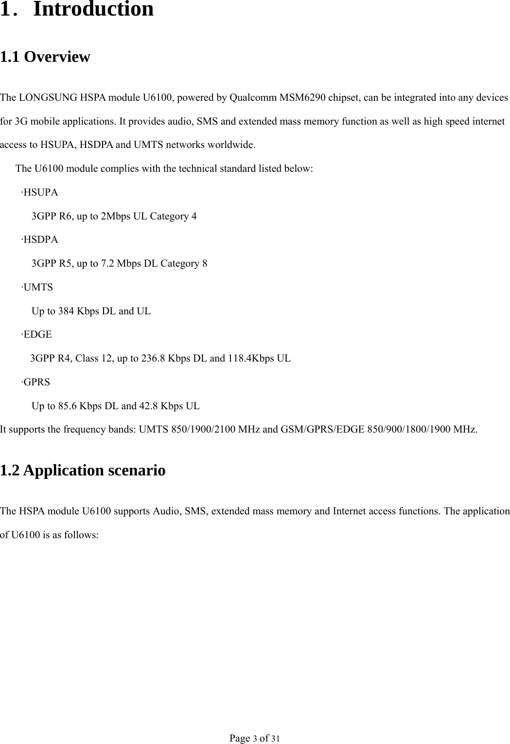
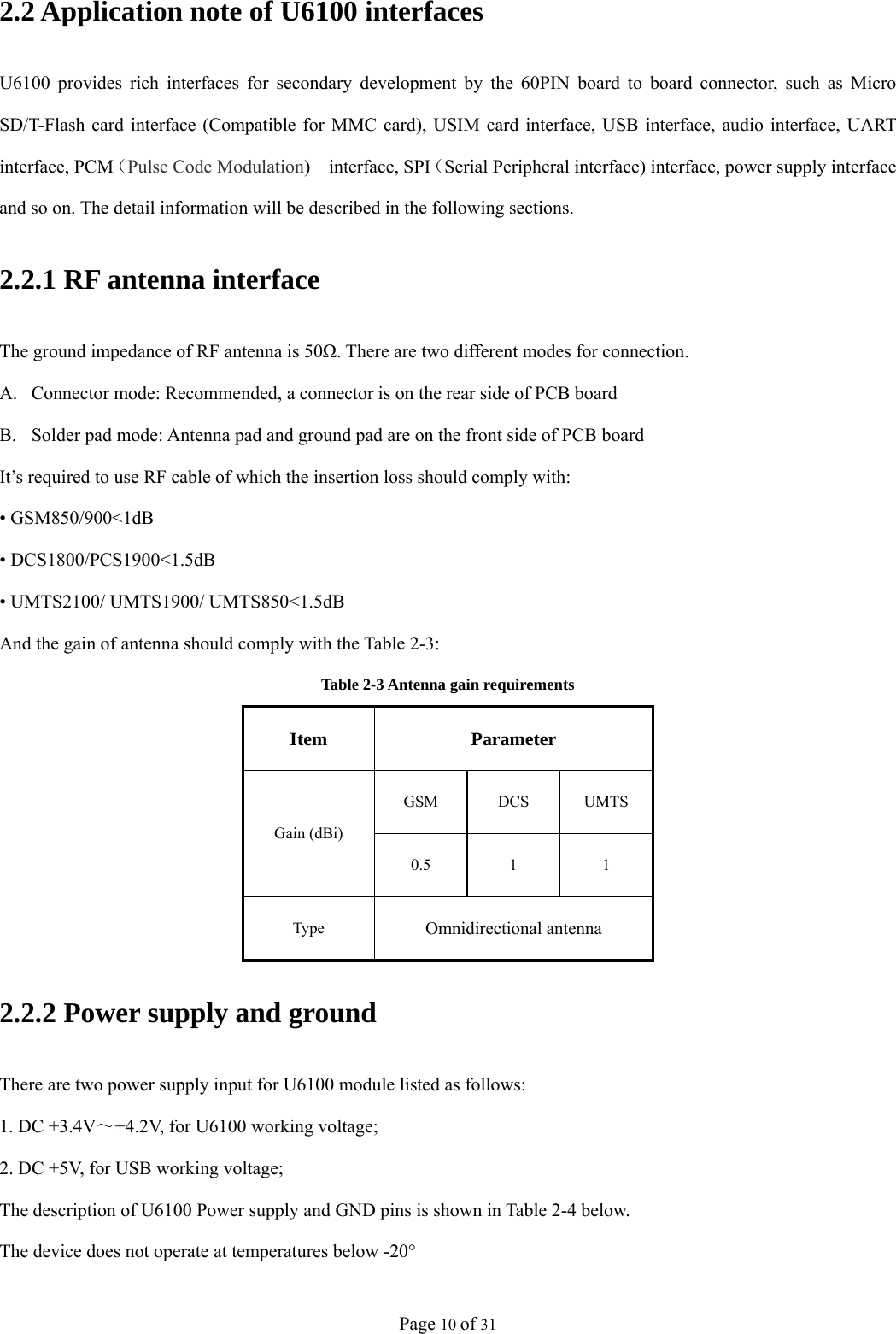
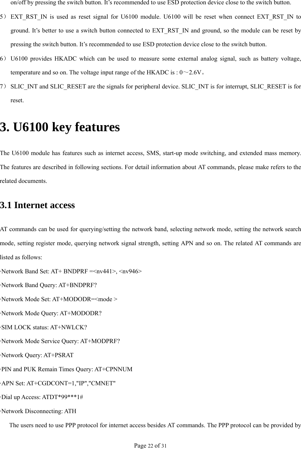
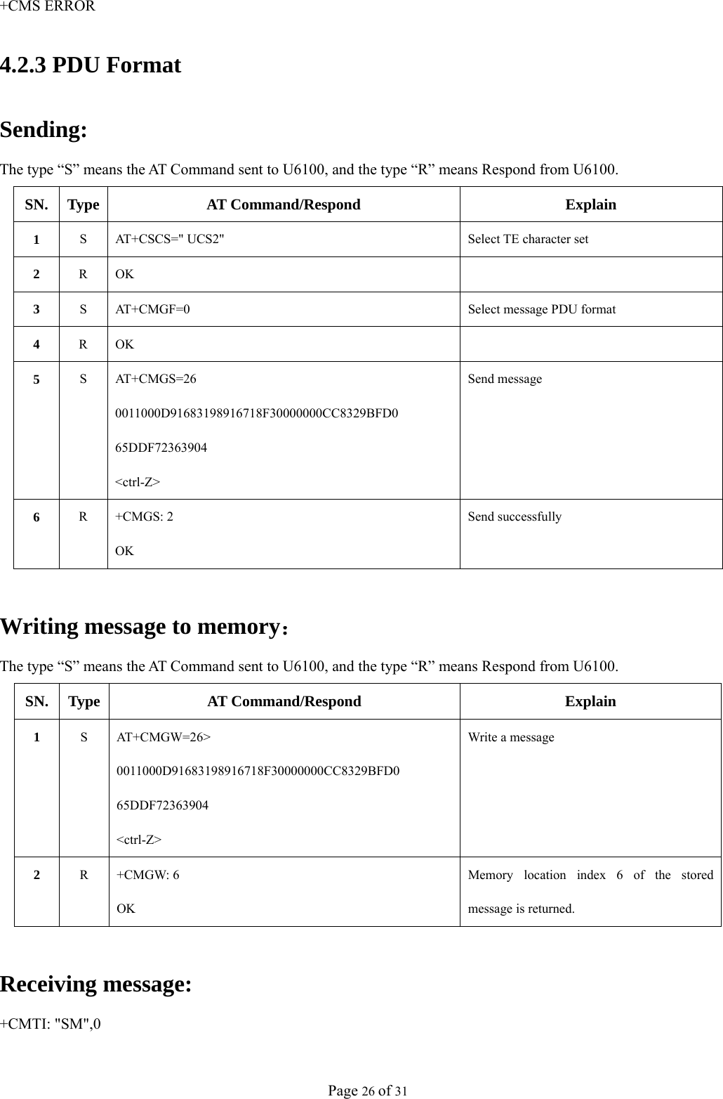
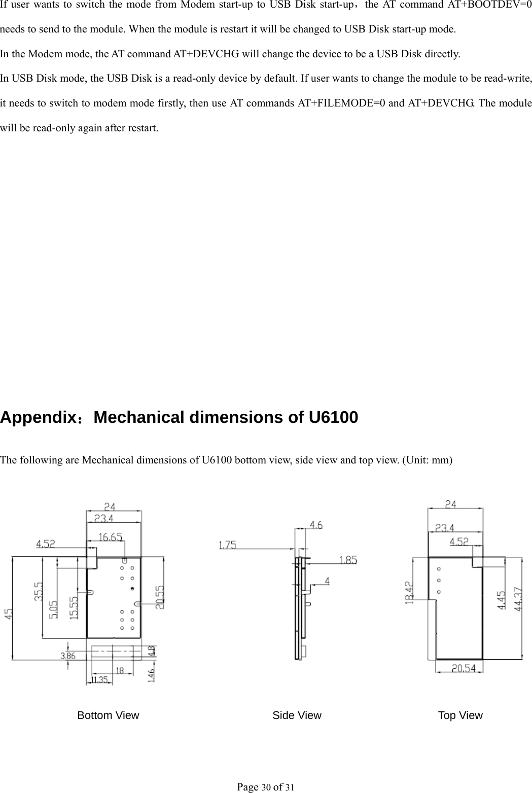
![Page 7 of 31 Table 2-2 The definition of board to board connector SN Definition Description Remark 1 VBAT Power Supply 2 VBAT Power Supply 3 VBAT Power Supply 4 VBAT Power Supply 5 VBAT Power Supply 6 VBAT Power Supply 7 GND Ground 8 GND Ground 9 MIC_P MIC Data+ MIC Interface 10 USB_DM USB Data- USB Interface 11 MIC_N MIC Data- MIC Interface 12 USB_DP USB Data+ USB Interface 13 GND Ground 14 GND Ground 15 EAROP Earphone Data+ Earphone Interface 16 GND Ground 17 EARON Earphone Data- Earphone Interface 18 USIM_RESET USIM Reset USIM Interface 19 GND Ground 20 USIM_DATA USIM Data USIM Interface 21 VREG_EXTUSIM USIM Power USIM Interface 22 GND Ground 23 PCM_DOUT/GPIO[103] PCM Data Output PCM Interface, can be used as GPIO 24 PCM_CLK/GPIO[80] PCM CLK PCM Interface, can be used as GPIO 25 PCM_DIN/GPIO[14] PCM Data Input PCM Interface, can be used as GPIO 26 GND Ground 27 GND Ground 28 HKADC External analog signal detecting](https://usermanual.wiki/Longcheer-Technology/U6100/User-Guide-1500060-Page-7.png)
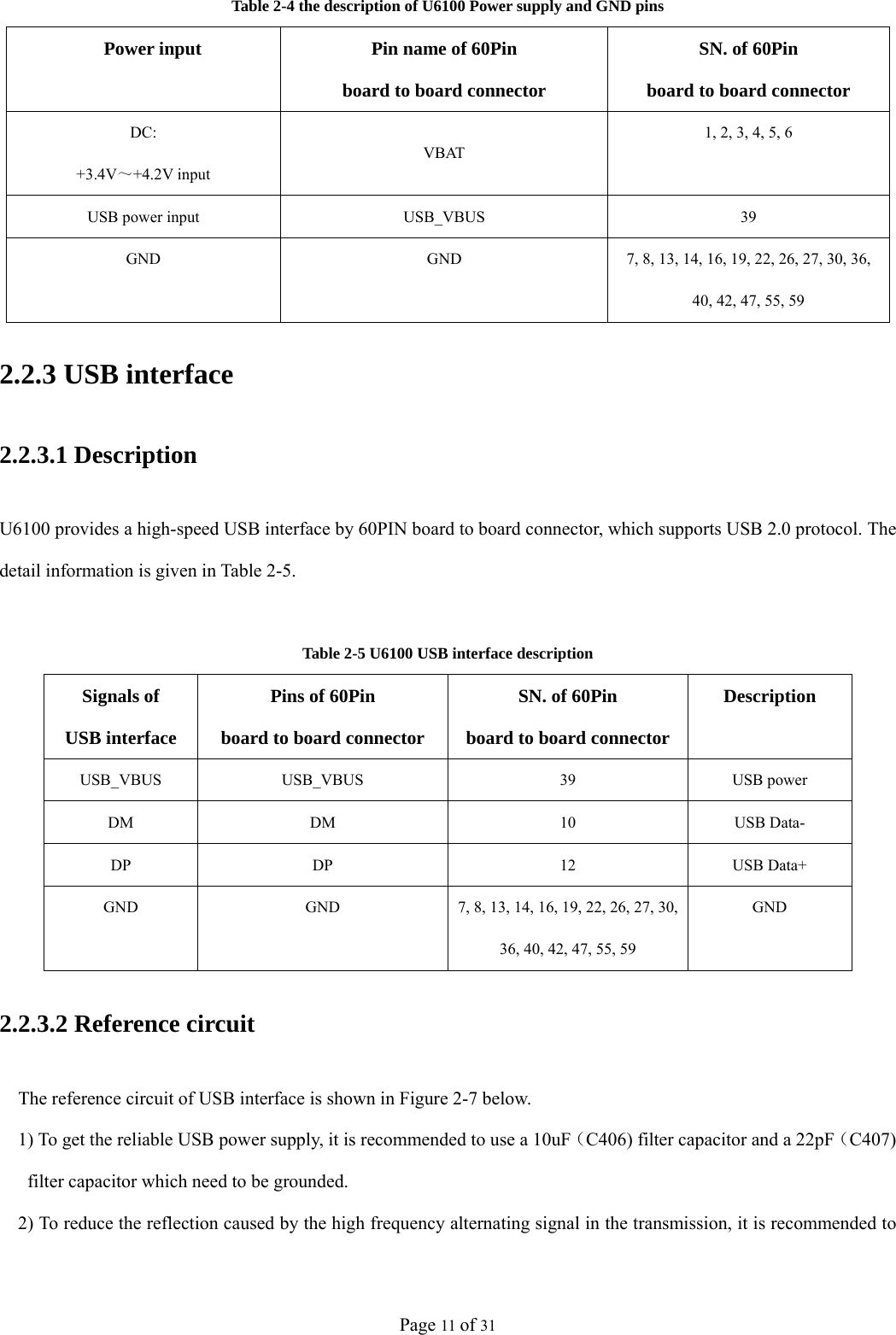
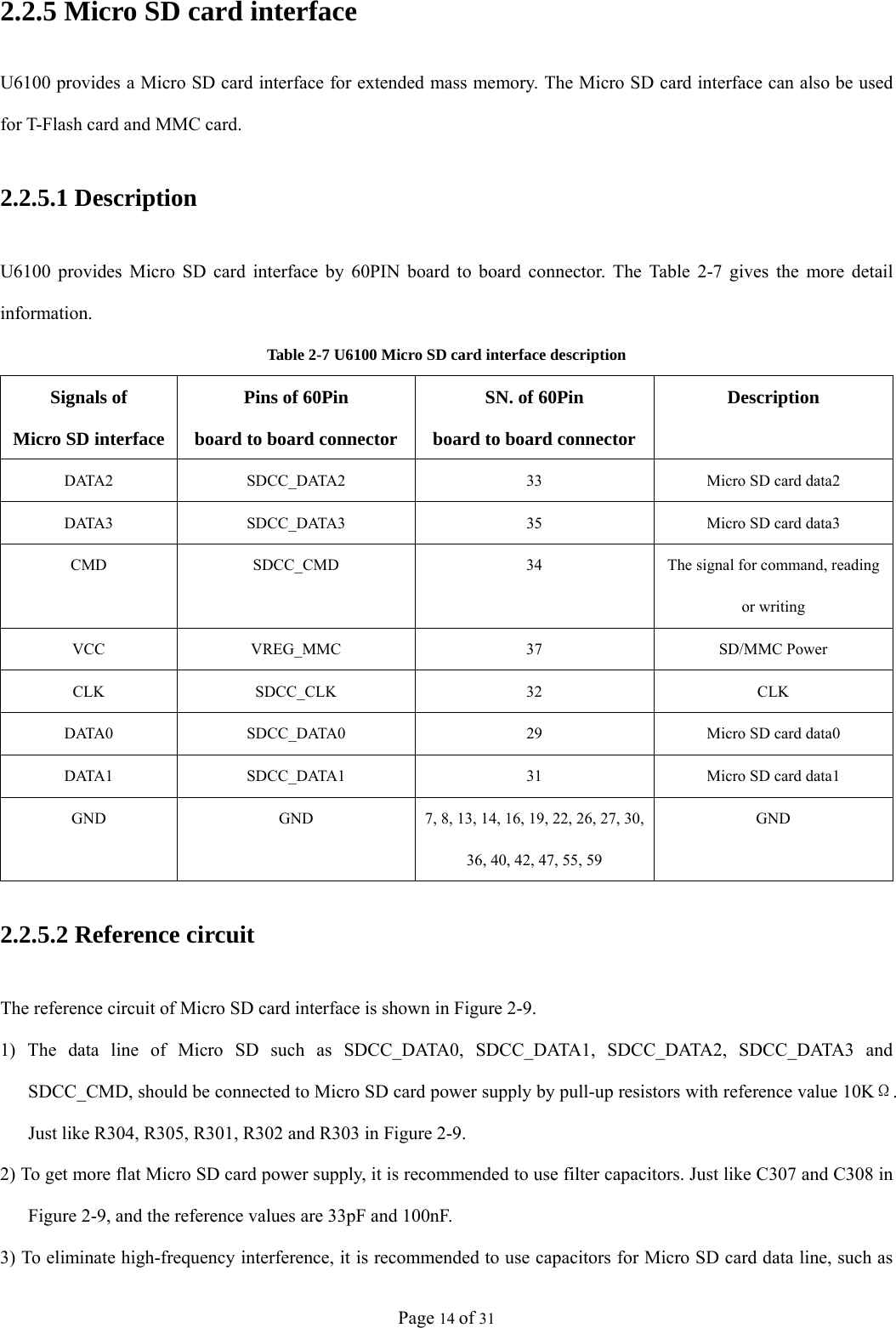
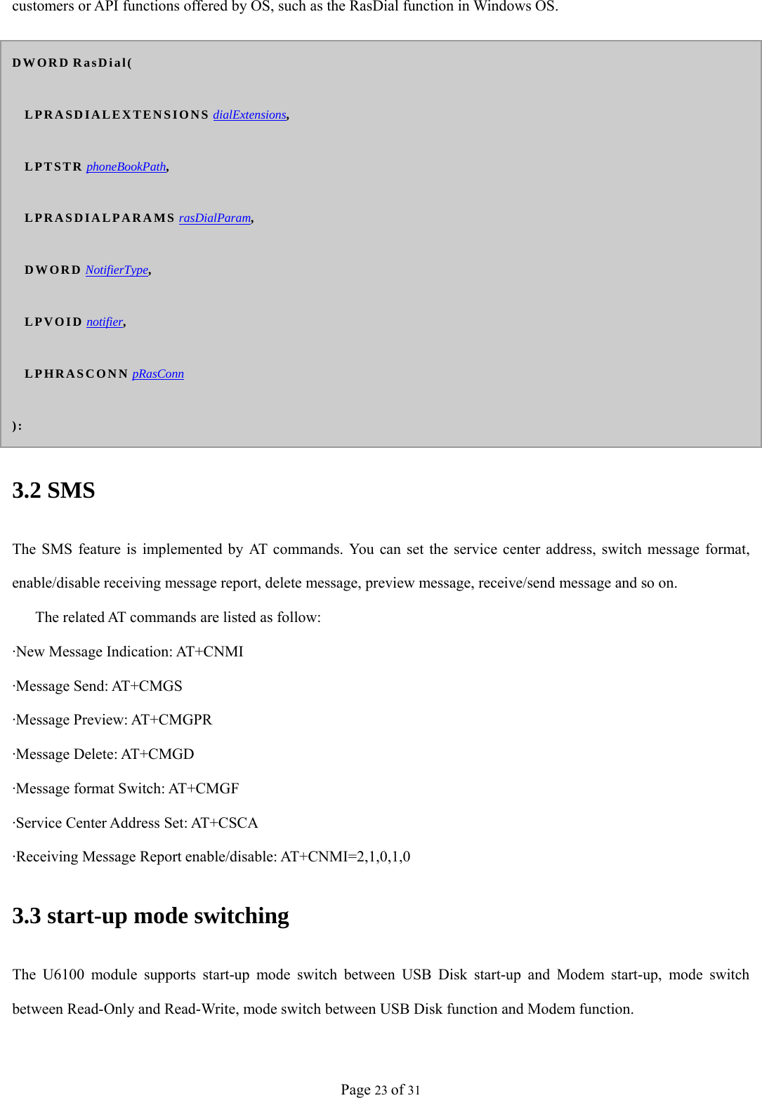
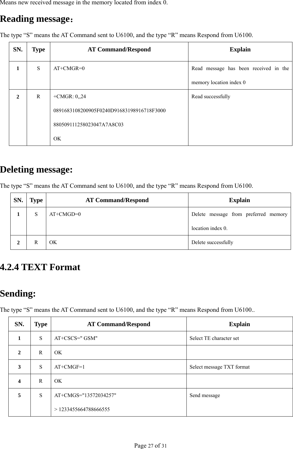
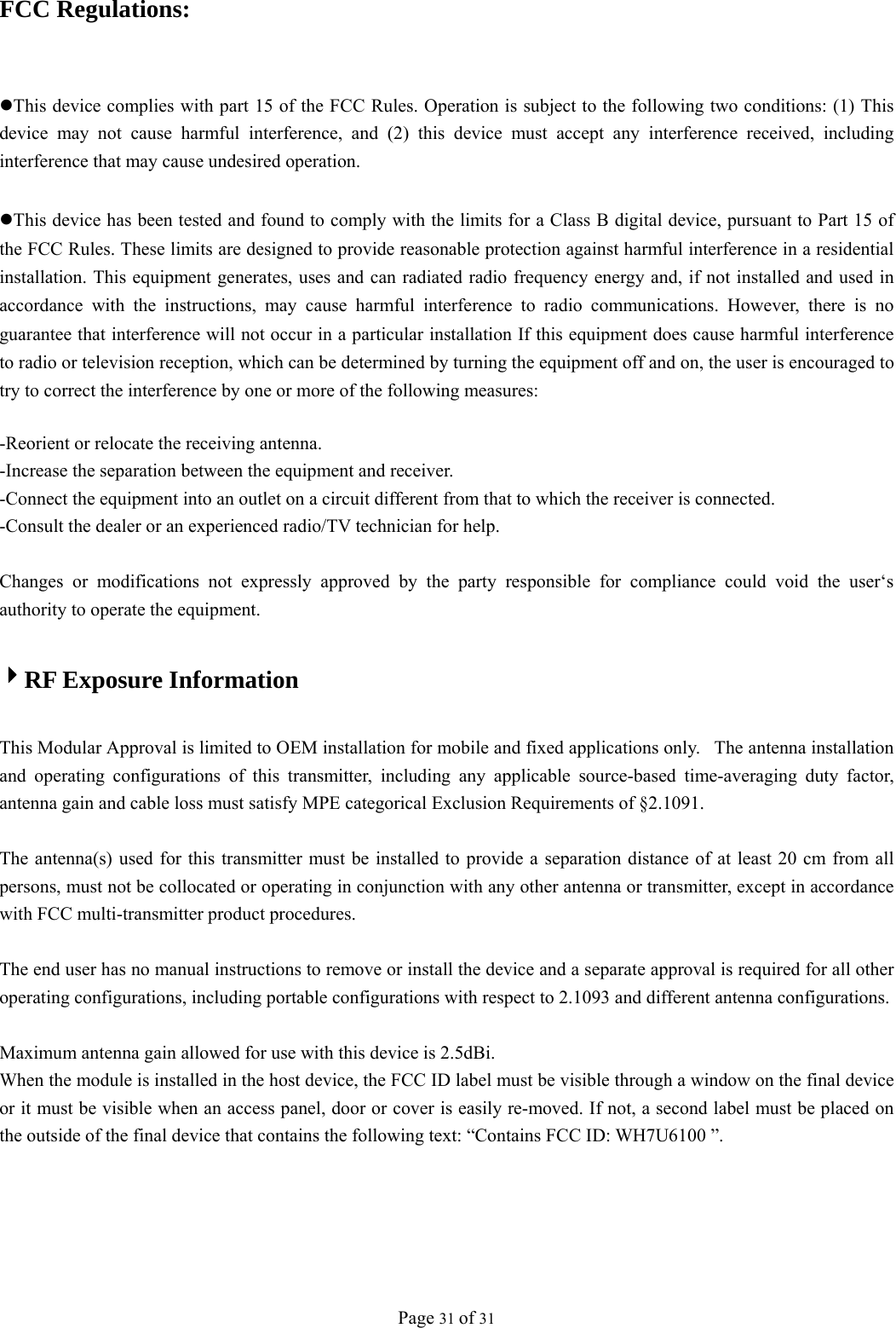
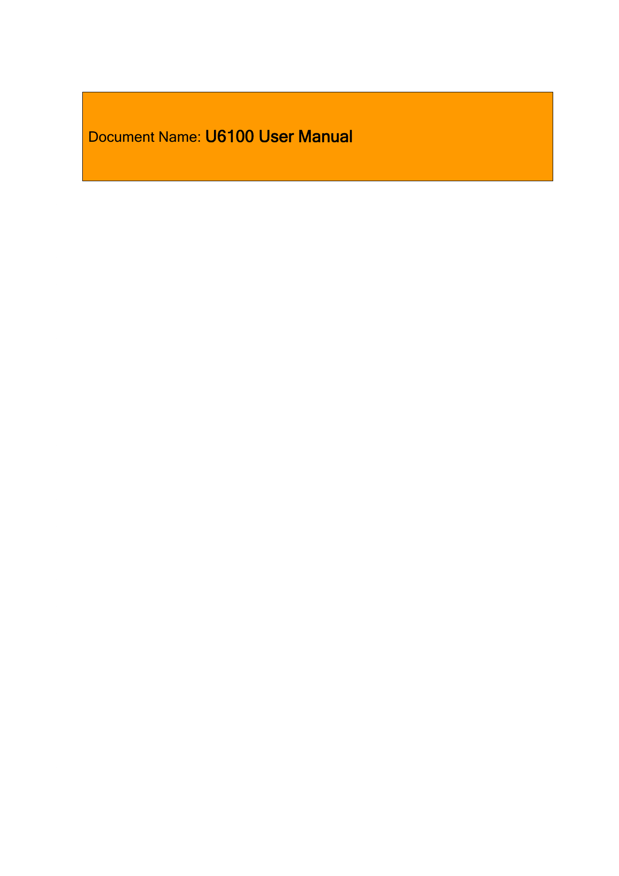
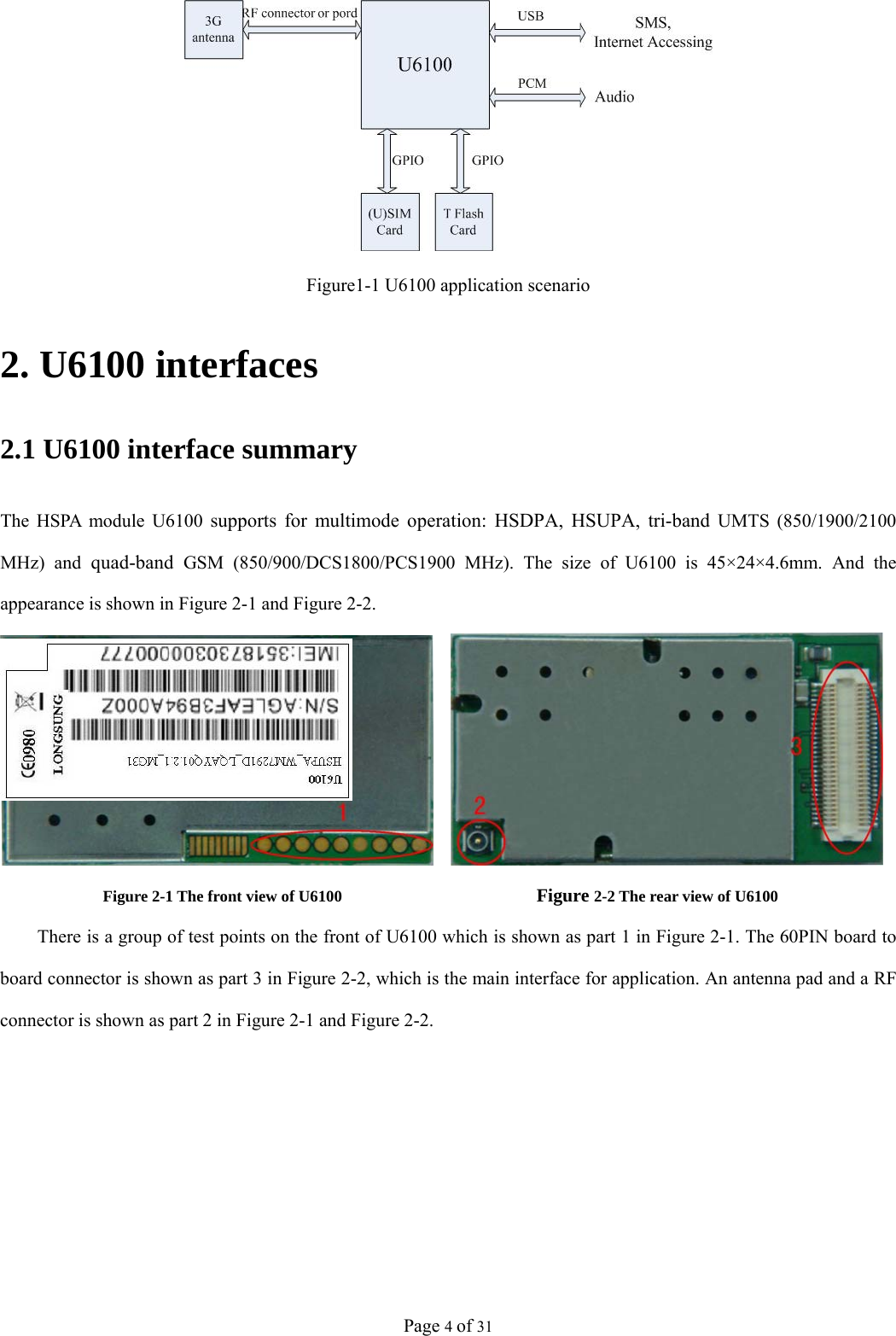
![Page 8 of 31 29 SDCC_DATA0/GPIO[32] Micro SD Data 0 Micro SD Interface, can be used as GPIO, SDCC_DATA0, SDCC_CLK, SDCC_CMD and VREG_MMC are compatible for MMC card 30 GND Ground 31 SDCC_DATA1/GPIO[99] Micro SD Data 1 Micro SD Interface, can be used as GPIO 32 SDCC_CLK/GPIO[31] Micro SD CLK Micro SD Interface, can be used as GPIO, SDCC_DATA0, SDCC_CLK, SDCC_CMD and VREG_MMC are compatible for MMC card 33 SDCC_DATA2/GPIO[100] Micro SD Data 2 Micro SD Interface, can be used as GPIO 34 SDCC_CMD/GPIO[30] Micro SD Command Micro SD Interface, can be used as GPIO. SDCC_DATA0, SDCC_CLK, SDCC_CMD and VREG_MMC are compatible for MMC card 35 SDCC_DATA3/GPIO[101] Micro SD Data 3 Micro SD Interface, can be used as GPIO 36 GND Ground 37 VREG_MMC Micro SD Power Micro SD Interface, can be used as GPIO. SDCC_DATA0, SDCC_CLK, SDCC_CMD and VREG_MMC are compatible for MMC card 38 USIM_CLK USIM CLK USIM Interface 39 USB_VBUS USB Power USB Interface 40 GND Ground 41 SLIC_RESET/GPIO[60] SLIC Reset Reset for peripheral device, can be used as GPIO 42 GND Ground 43 SLIC_INT/GPIO[59] SLIC Interrupt Interrupt for peripheral device, can be used as GPIO 44 SPI_CLK/GPIO[57] SPI CLK SPI Interface, can be used as GPIO 45 VREG_MSMP VREG_MSMP voltage output 46 SPI_DOUT/GPIO[55] SPI Data Output SPI Interface, can be used as GPIO 47 GND Ground 48 SPI_DIN/GPIO[56] SPI Data Input SPI Interface, can be used as GPIO 49 PWM_OUT PWM Output 50 SPI_CS/GPIO[58] SPI CS SPI Interface, can be used as GPIO 51 VCOIN VRTC 52 KPD_PWR_N Power On](https://usermanual.wiki/Longcheer-Technology/U6100/User-Guide-1500060-Page-8.png)
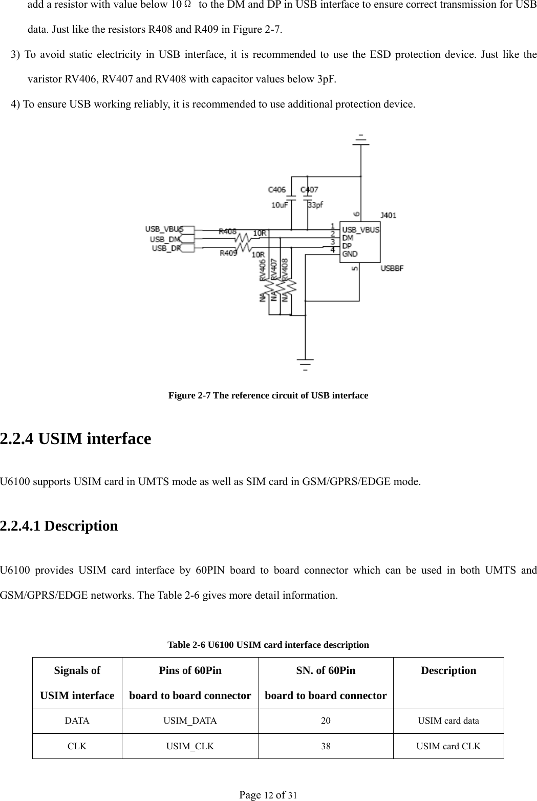
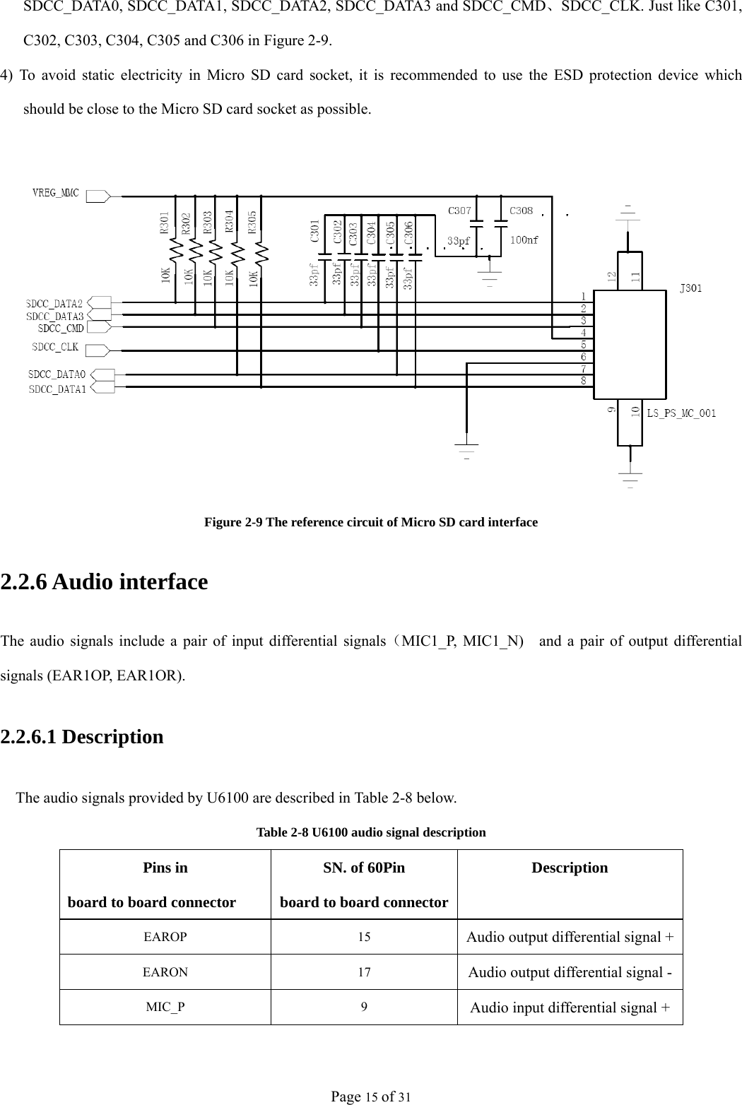
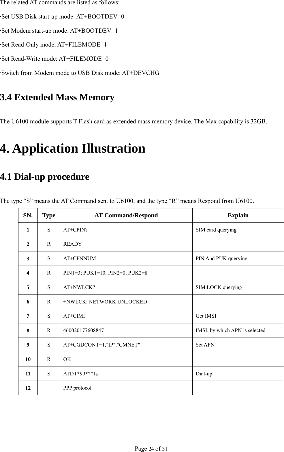
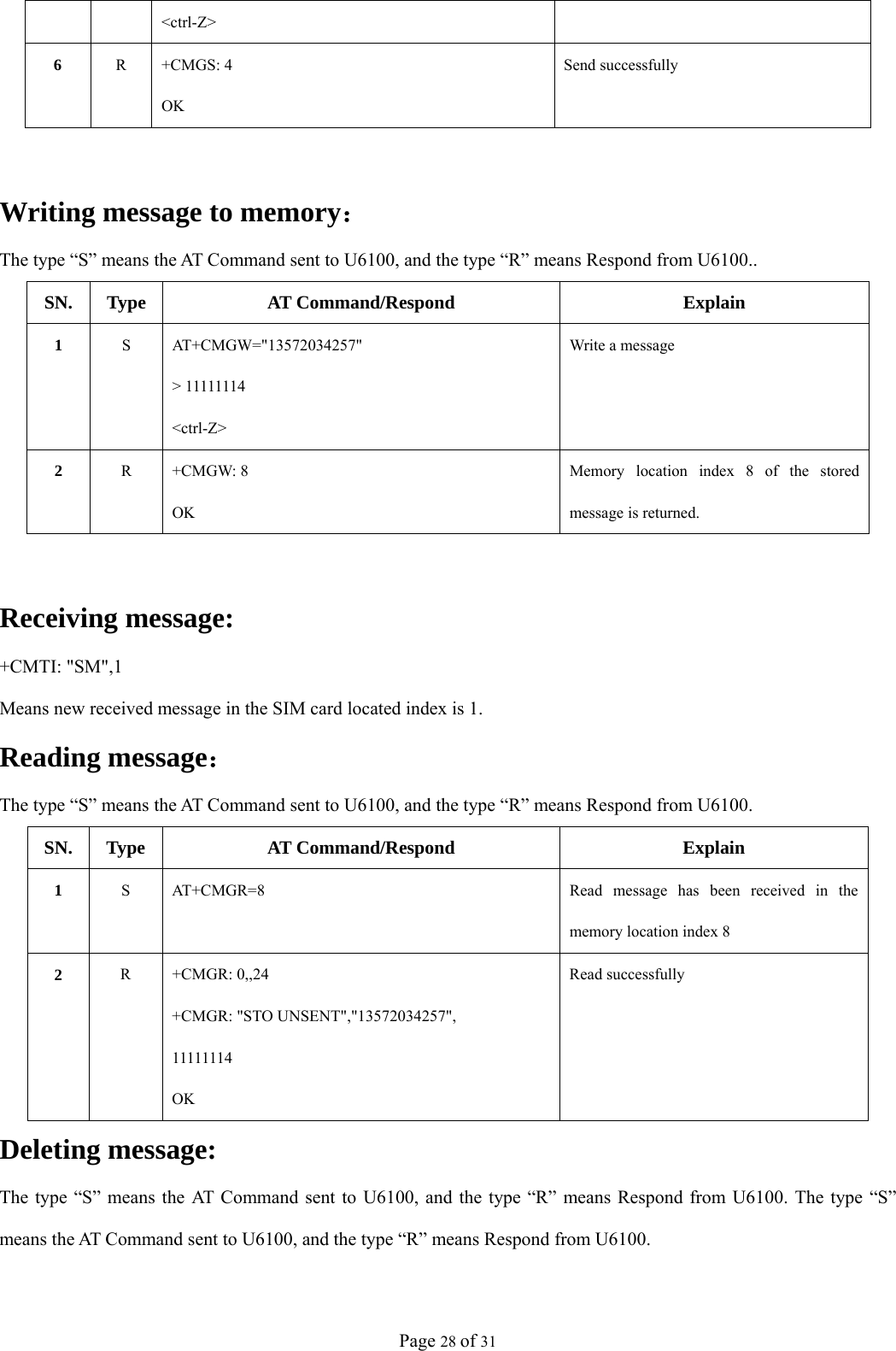
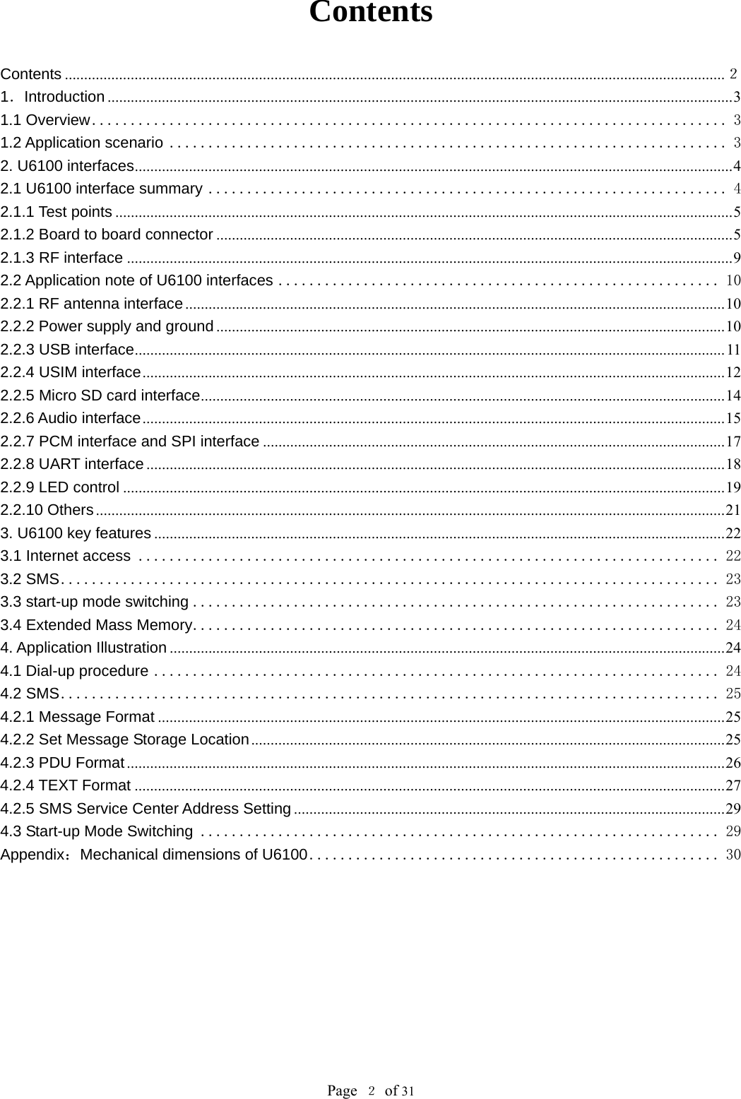
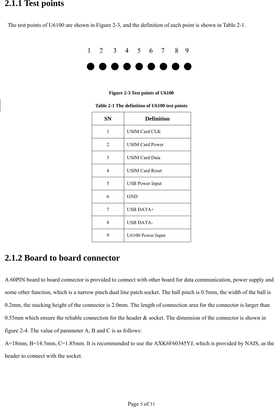
![Page 9 of 31 53 EXT_RST_IN Reset 54 UART_TX/GPIO[95] Tx in UART UART, can be used as GPIO 55 GND Ground 56 UART_RX/GPIO[96] Rx in UART UART, can be used as GPIO 57 PCM_SYNC/GPIO[102] PCM Synchronous Signal PCM Interface, can be used as GPIO 58 LED_CTL_G The Green LED Control 59 GND Ground 60 LED_CTL_R The RED LED Control 2.1.3 RF interface The U6100 module provides an interface for RF antenna which has two different modes for connection. Connector mode: U6100 uses MURATA’s MM9329-2700RA1 RF connector on the rear side, it is recommend to use MURATA’s MXTK92XXXXX as matching connector. Please refer to MURATA’s MXTK92XXXXX documents for more information. Solder pad mode: The antenna can also be soldered to the pad on the module which has a ground pad close to the antenna pad. The RF connector is shown in Figure 2-6. Figure 2-6 The sketch map of RF connector](https://usermanual.wiki/Longcheer-Technology/U6100/User-Guide-1500060-Page-9.png)