MMB Research CSB04PA1X MMB Networks ZigBee/Thread/BLE Module User Manual
MMB Research Inc. MMB Networks ZigBee/Thread/BLE Module
UserManual.wiki
>
MMB Research
>
CSB04PA1X User Manual
User Manual
Navigation menu
Upload a User Manual
Namespaces
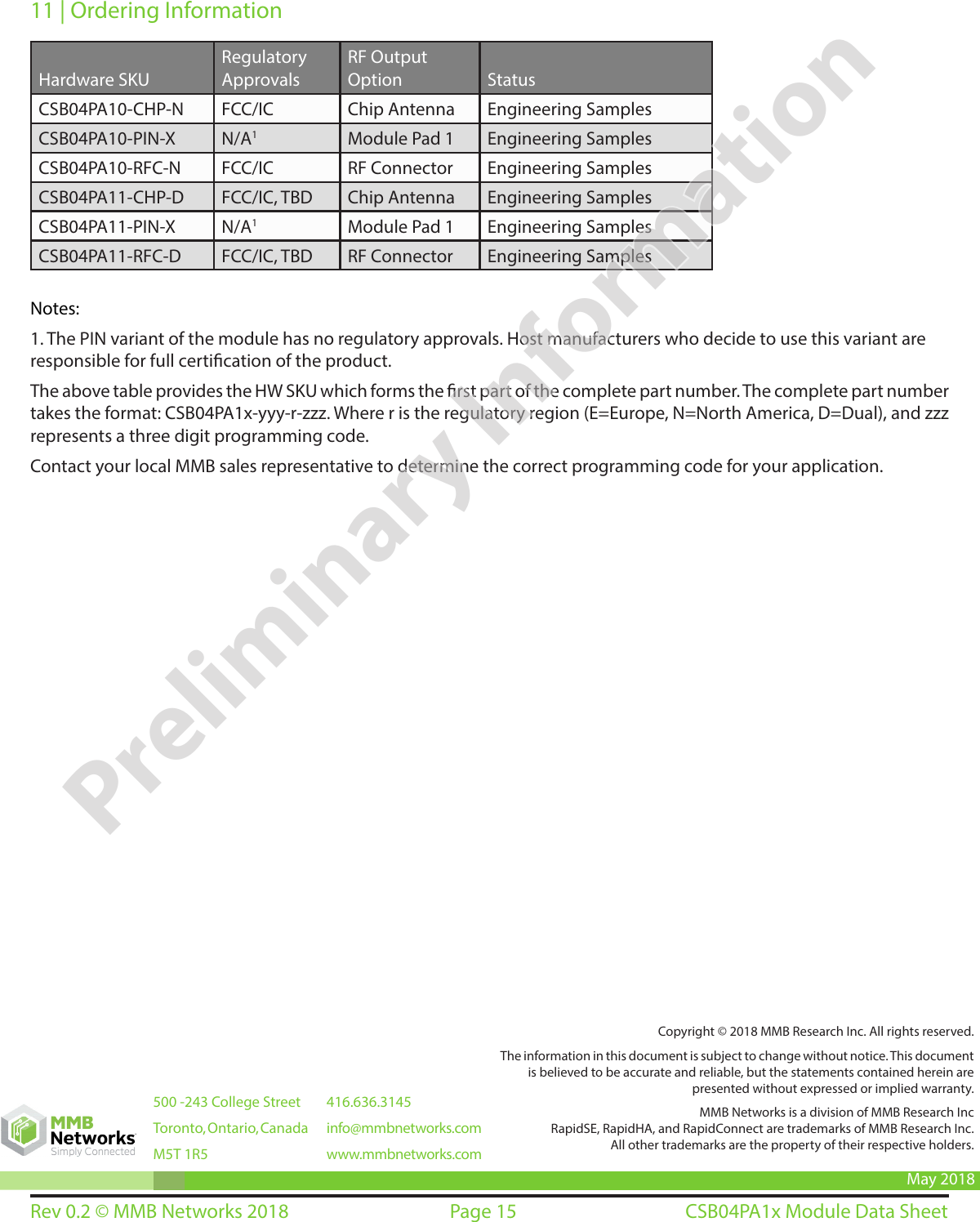
Wiki Guide
HTML
PDF
Info
Views
User Manual
Discussion / Help
Navigation