MMB Research CSB04PA1X MMB Networks ZigBee/Thread/BLE Module User Manual
MMB Research Inc. MMB Networks ZigBee/Thread/BLE Module
User Manual

Page 1Rev 0.3 © MMB Networks 2018 CSB04PA1x Module Data Sheet
Pre-loaded with RapidConnect rmware Ensures compatibility with latest Zigbee, Thread and
BLE specications
MMB Networks EFR32 Zigbee/Thread/BLE Module
CSB04PA10 / PA11 Document Rev 0.3
The MMB Networks CSB04PA1x family is the latest generation
Zigbee, Thread, and BLE capable module. Based on the EFR32
multi-protocol IC from Silicon Labs, the CSB04PA1x are drop-in
Zigbee 3.0, Thread and BLE 5.0 solutions. Preloaded with MMB
Networks’ RapidConnect Home Automation application, it oers
hardware vendors an easy way to integrate a fully-implemented,
automated Zigbee, Thread or BLE Home Automation platform into
their existing devices.
MMB Networks oers a variety of hardware and software
development tools to facilitate integration. For more information,
please visit
http://www.mmbnetworks.com
Features Benets
+19, and +10dBm transmit power options Power and price optimized to meet end product
transmit power requirements
Built on Silicon Labs EFR32 Wireless Gecko Family Industry leading 802.15.4 MCU ensures best-in-class
performance
Certied application layer, onboard stack, antenna and
regulatory approvals
Provides rapid time-to-market and short
implementation time
Up to 121 dB link budget Delivers unmatched range for dicult installations
SMD Chip Antenna or U.FL RF connector options Allows for external antennas where required
15.88mm x 12.6mm x 2.4mm module size Tiny module size will t in the most miniature
applications
15 GPIO (General Purpose Input/Output) connections Flexibility to drive simple to complex devices
Preliminary Information

Page 2Rev 0.3 © MMB Networks 2018 CSB04PA1x Module Data Sheet
Contents
1 | General Information ......................................................................................................................................................3
2 | Memory .............................................................................................................................................................................. 3
3 | Module Pinout .................................................................................................................................................................3
3.1 | Debug and Programming Interface ................................................................................................................4
4 | Electrical Specications ................................................................................................................................................4
4.1 | Absolute Maximum Ratings ............................................................................................................................... 4
4.2 | Recommended Operating Conditions ........................................................................................................... 4
4.3 | DC Electrical Characteristics ...............................................................................................................................5
4.3.1 | Typical Transmit Performance Curves (Supply Current vs. Tx Power Setting) ...............................5
5 | RF Specications .............................................................................................................................................................6
5.1 | Receive Specications ..........................................................................................................................................6
5.2 | Transmit Specications ........................................................................................................................................6
5.2.1 | Typical Transmit Performance Curves (Output Power vs. Tx Power Setting) .................................7
6 | Functional Specications .............................................................................................................................................7
6.1 | Serial Ports ................................................................................................................................................................ 7
7 | Mechanical Specications ...........................................................................................................................................8
7.1 | Module Physical Dimensions and Host PCB Antenna Keep-out ...........................................................8
7.2 | Recommended Land Pattern (Surface Mount) ...........................................................................................9
7.3 | RF Connector Dimensions ............................................................................................................................... 10
7.4 | Label Drawings .................................................................................................................................................... 10
8 | Soldering Temperature Time Prole for reow soldering (Lead-free solder) ......................................... 11
9 | Regulatory Approvals................................................................................................................................................. 11
9.1 | Federal Communications Commission (FCC - US) ...................................................................... 11
9.2 | Industry Canada (IC) .......................................................................................................................................... 13
9.3 | RoHS Compliance .................................................................................................................................. 14
9.4 | FCC & IC Compliance ............................................................................................................................ 14
10 | Revision History ......................................................................................................................................................... 14
11 | Ordering Information .............................................................................................................................................. 15
Preliminary Information
Page 3Rev 0.3 © MMB Networks 2018 CSB04PA1x Module Data Sheet
1 | General Information
Note that some of the specications refer to either the “EFR32MG13” chip or the “Module”. Specications cited as EFR32 are
taken from the EFR32MG13 datasheet (this should also be noted where referred to). Module means measurements taken
with our production module.
2 | Memory
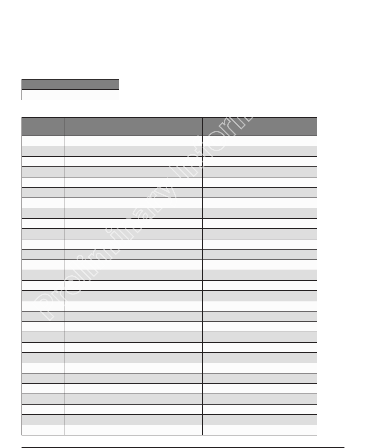
3 | Module Pinout
Module Pad Function
EFR32 Pin Name
(number)
Mini Simplicity
Debug Interface ADC Capable
1 2.4GHz antenna line out 2G4RF_IOP (12)
2 Module Ground
3 EFR32 GPIO, Port D #13 PD13 (14) Yes
4 EFR32 GPIO, Port D #14 PD14 (15) Yes
5 EFR32 GPIO, Port D #15 PD15 (16) Yes
6 EFR32 GPIO, Port A #1 PA1 (18) UART1_RX Yes
7 EFR32 GPIO, Port A #0 PA0 (17) UART1_TX Yes
8 Digital I/O Power Supply IOVDD (30)
9 EFR32 GPIO, Port B #11 PB11 (19) Yes
10 EFR32 GPIO, Port B #12 PB12 (20) PTI_DATA Yes
11 Module Ground
12 Module Ground
13 Module Ground
14 EFR32 GPIO, Port B #13 PB13 (21) PTI_FRAME Yes
15 EFR32 GPIO, Port B #14 PB14 (23) Yes
16 EFR32 GPIO, Port B #15 PB15 (24) Yes
17 Module Ground GND
18 Module Main Power VAEM
19 Module Ground
20 EFR32 GPIO, Port C #10 PC10 (31) Yes
21 EFR32 GPIO, Port C #11 PC11 (32) Yes
22 Module Ground
23 Reset input, active low RESETn (8) RESET_N
24 EFR32 GPIO, Port F #0 PF0 (1) SW_CLK Yes
25 EFR32 GPIO, Port F #1 PF1 (2) SW_DIO Yes
26 EFR32 GPIO, Port F #2 PF2 (3) SW_O Yes
27 Module Ground
28 RFGND1
29 RFGND2
Preliminary Information
RAM (kB) On-Chip Flash (kB)
64 512
Page 4Rev 0.3 © MMB Networks 2018 CSB04PA1x Module Data Sheet
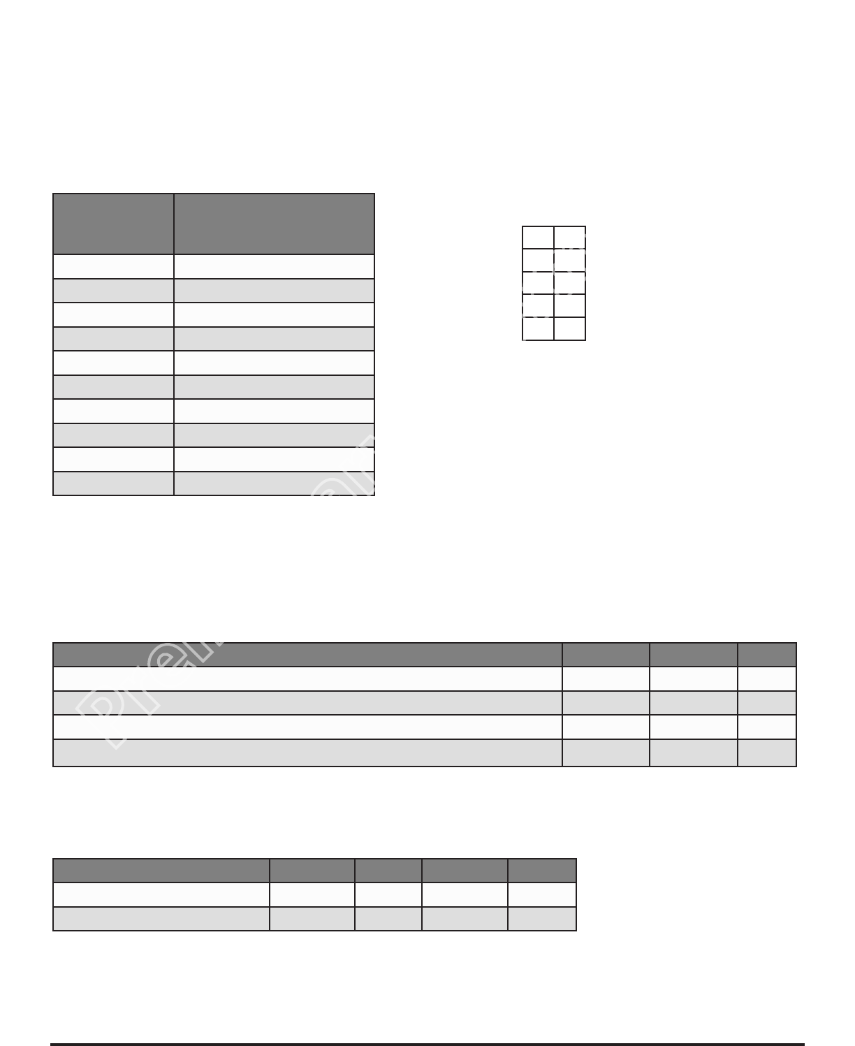
3.1 | Debug and Programming Interface
In order to access the EFR32 for programming and debug purposes, it is recommended that the designer incorporate
Silcon Labs 10-pin Mini Simplicity connector.
The following table shows a pin mapping between Silicon Labs 10-pin Mini Simplicity connector and the module, and the
graphic to the right displays the layout of the Mini Simplicity connector.
4 | Electrical Specications
4.1 | Absolute Maximum Ratings
Parameter Minimum Maximum Units
Supply Voltage (VCC) 0 3.6 V
Voltage on any GPIO -0.3 VCC + 0.3 V
Ambient Operating Temperature (standard version) -40 85 °C
Storage Temperature -50 150 °C
4.2 | Recommended Operating Conditions
Silicon Labs
Simplicity
Studio Port Pin Module Pad
1 8 (Digital I/O Power Supply)
2 17 (Module Ground)
3 23 (Reset input, active low)
4 6 (EFR32 GPIO, Port A #1)
5 7 (EFR32 GPIO, Port A #0)
6 26 (EFR32 GPIO, Port F #2)
7 25 (EFR32 GPIO, Port F #1)
8 24 (EFR32 GPIO, Port F #0)
9 14 (EFR32 GPIO, Port B #13)
10 10 (EFR32 GPIO, Port B #12)
Parameter Minimum Typical Maximum Units
Supply Voltage (VCC) 2.0 3.3 3.6 V
Temperature Range -40 85 °C
1 2
3 4
5 6
7 8
9 10
VAEM
RST
VCOM_TX
SWDIO
PTI_FRAME
GND
VCOM_RX
SWO
SWCLK
PTI_DATA
Preliminary Information

Page 5Rev 0.3 © MMB Networks 2018 CSB04PA1x Module Data Sheet
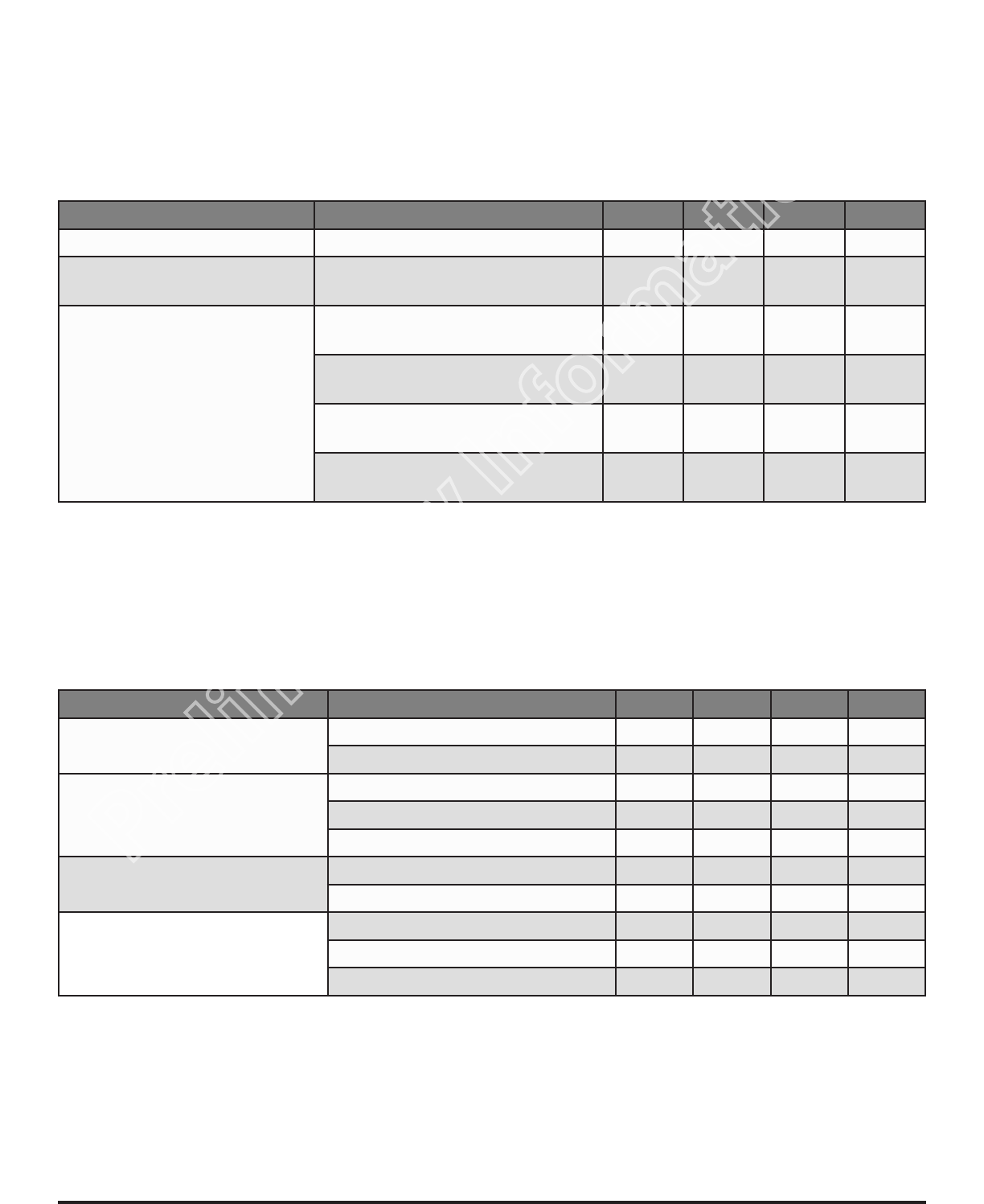
4.3 | DC Electrical Characteristics
4.3.1 | Typical Transmit Performance Curve (Supply Current vs. Tx Power)
Note: The graph above is for the PA10 variant. For the PA11 module, the maximum output power is limited to 10.5dBm
Parameter Test Condition Minimum Typical Maximum Units
TX Current
At 25 °C, VCC = 3.3v, normal mode, 19 dBm 138 mA
At 25 °C, VCC = 3.3v, normal mode, 10 dBm 49 mA
RX Current
At 25 °C, VCC = 3.3v, normal mode, 2.4 GHz, CPU
asleep 6 mA
At 25 °C, VCC = 3.3v, normal mode, 2.4 GHz, CPU
running 14 mA
Deep Sleep
Current
At 25 °C, VCC = 3.3v, shutdown mode. Full RAM
retention and RTCC running from LFXO (EM2
mode) 2.3 μA
0
20
40
60
80
100
120
140
012345678910 11 12 13 14 15 16 17 18 19 20
Icc(mA)
PowerSetting
Supply Current(mA)vs.TXPowerSetting
Preliminary Information
Page 6Rev 0.3 © MMB Networks 2018 CSB04PA1x Module Data Sheet
5 | RF Specications
5.1 | Receive Specications
Note: The Typical number indicates one standard deviation above the mean, measured at room temperature (25°C). The
Min and Max numbers were measured over process corners at room temperature.
Parameter Test Condition Min Typical Max Units
Frequency range 2400 2483.5 MHz
Sensitivity - Zigbee and Thread
1% PER, 20 byte packet dened by
IEEE 802.15.4-2003 -102 dBm
Sensitivity - Bluetooth Low Energy
0.1% BER. Signal is reference signal1, bit
rate=125kbps -103 dBm
0.1% BER. Signal is reference signal1, bit
rate=500kbps -99 dBm
0.1% BER. Signal is reference signal1, bit
rate=1Mbps -95 dBm
0.1% BER. Signal is reference signal1, bit
rate=2Mbps -91 dBm
Notes:
1. Reference signal is dened 2GFSK at -67dBm, Modulation index=0.5, BT=0.5, desired data=PRBS9, interferer
data=PRBS15, frequency accuracy better than 1 ppm
5.2 | Transmit Specications
Parameter Test Condition Min Typical Max Units
802.15.4 output power at highest
power setting, general limit1
CSB04PA10219.2 dBm
CSB04PA11210.5 dBm
802.15.4 Channel 26 output power
CSB04PA10-CHP 15 dBm
CSB04PA11-CHP 10.5 dBm
CSB04PA1X-RFC38dBm
BLE output power at highest power
setting, general limit1
CSB04PA10219.2 `` dBm
CSB04PA11210.5 dBm
BLE Channel 26 output power
CSB04PA10-CHP 19.2 dBm
CSB04PA10-RFC 15 dBm
CSB04PA11210.5 dBm
Notes:
1. RF channel 26 operates at special reduced power levels.
2. If antenna conguration (CHP- chip antenna or RFC - RF connector) is not specied then value applies to both
congurations.
3. 1X includes CSB04PA10, and PA11 variants
Preliminary Information

Page 7Rev 0.3 © MMB Networks 2018 CSB04PA1x Module Data Sheet
5.2.1 | Typical Transmit Performance Curves (Output Power vs. Tx Power Setting)
Note: The graph above is for the PA10 variant. For the PA11 module, the maximum output power is limited to 10.5 dBm.
6 | Functional Specications
6.1 | Serial Ports
Refer to the EFR32MG13 data sheet for functionality and associated GPIO pinouts.
Note: The module pinout table in section 3 of this document provides a cross reference between the MMB module pins
and the EFR32 GPIO.
Note 2: The RapidConnect rmware supports UART communication with a baud rate of 115.2kbps. However, MMB can
modify this conguration as necessary through a Non-Recurring Engineering engagement.
0
2
4
6
8
10
12
14
16
18
20
0246810 12 14 16 18 20
Output Power(dBm)
PowerSetting
OutputPower(dBm)vs.TXPowerSetting
Preliminary Information
Page 8Rev 0.3 © MMB Networks 2018 CSB04PA1x Module Data Sheet
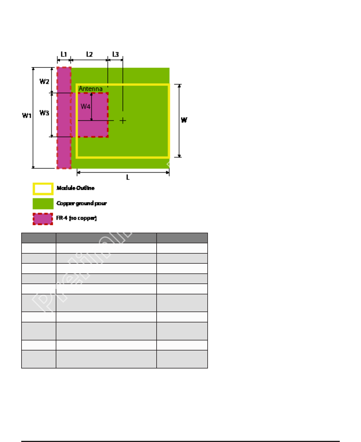
7 | Mechanical Specications
7.1 | Module Physical Dimensions and Host PCB Antenna Keep-out
Symbol Description Distance
L Length of the module 15.88 mm
W Width of the module 12.60 mm
H Height of the module 2.88 mm
L1 Second keep-out length 2.27 mm
L2 First keep-out length 6.43mm
L3
Length from module centre to edge
of rst keep-out 2.65 mm
W1 Second keep-out width 17.41mm
W2
Distance from edge of rst keep-out
to edge of second keep-out 4.41mm
W3 First keep-out width 7.62mm
W4
Width from module centre to edge
of rst keep-out 5.4 mm
Note: The above table and recommendation apply to CSB04PA1x-CHP products only. Copper keep-out regions apply
to all PCB layers. CSB04PA1x-RFC have identical dimensions but do not require an antenna keep-out.
The CSB04PA1x family of devices use a System on Module (SOM) package process technology.
Preliminary Information
Page 9Rev 0.3 © MMB Networks 2018 CSB04PA1x Module Data Sheet
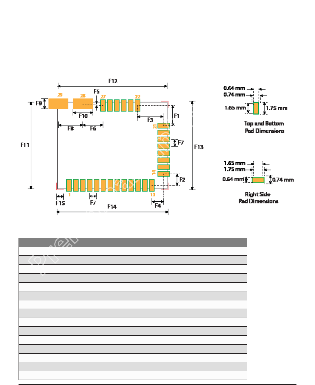
7.2 | Recommended Land Pattern (Surface Mount)
The diagram below shows the recommended dimensions and arrangement of the pads for the module. The PCB upon
which the module will be mounted should not include any non-ground traces or vias on the top layer directly under the
module. All copper features other than the module mounting pads, including ground vias, should be tented or covered
with soldermask to avoid coming in contact with the module’s traces and producing unexpected behavior. If it is absolutely
necessary to include traces and/or vias under the module due to space constraints, then a customer can elect to do so at
their own risk. MMB can provide a Hardware Designer Package to show the module’s footprint and drill locations, which
must not line up with the daughtercard’s drill locations.
Note: Green box is the size of the top metal layer. Orange is the opening in the soldermask layer.
Symbol Description Distance
F1 Distance pad centre to pad centre (vertical: pad 21 to 22) 2.93 mm
F2 Distance pad centre to pad centre (vertical: pad 13 to 14) 1.67 mm
F3 Distance pad centre to pad centre (horizontal: pad 21 to 22) 3.77 mm
F4 Distance pad centre to pad centre (horizontal: pad 13 to 14) 1.69 mm
F5 Distance pad centre to RFGND centre (vertical: pad 27 to 28) 0.26 mm
F6 Distance pad centre to RFGND centre (horizontal: pad 27 to 28) 2.90mm
F7 Pitch (pad to pad) 1.02 mm
F8 Pitch (RFGND pad to RFGND pad) 3.52mm
F9 RFGND pad metal and soldermask width 1.47mm
F10 RFGND pad metal and soldermask length 2.78mm
F11 Module width 12.60 mm
F12 Module length 15.88 mm
F13 Width between silkscreen corners 12.90 mm
F14 Length between silkscreen corners 16.18 mm
F15 Size of silkscreen corner line 1 mm
Preliminary Information
Page 10Rev 0.3 © MMB Networks 2018 CSB04PA1x Module Data Sheet
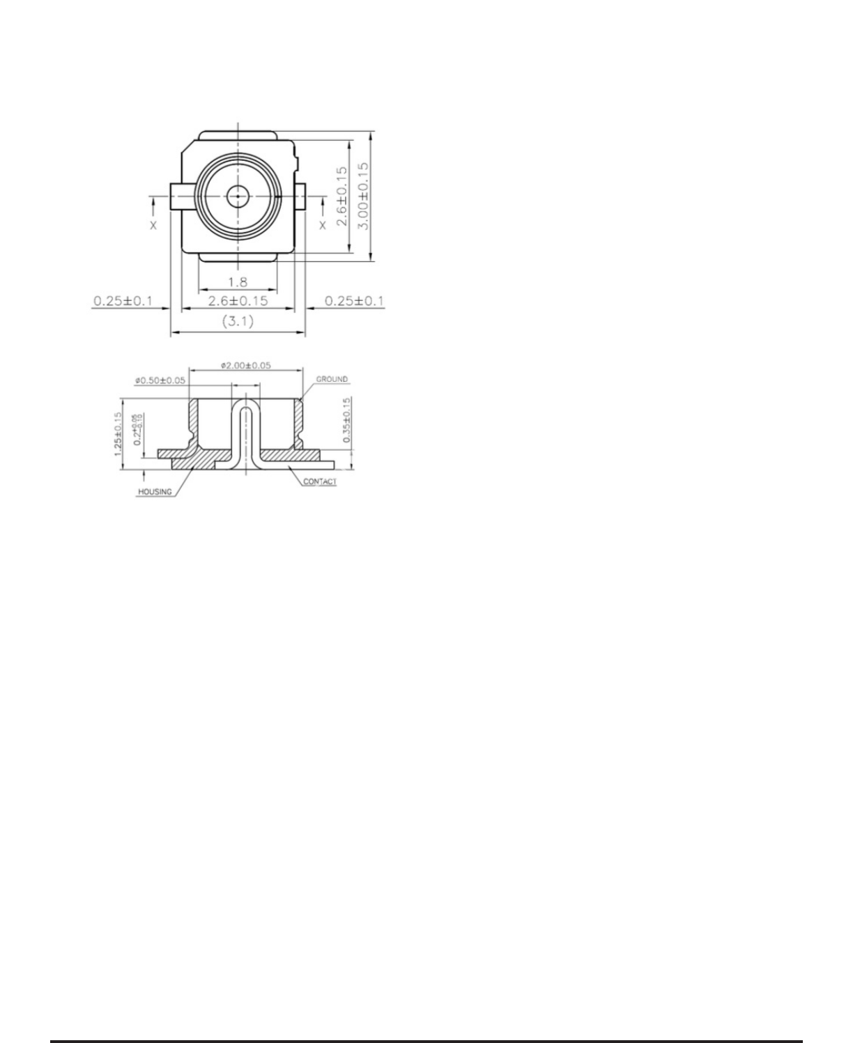
7.3 | RF Connector Dimensions
The diagram below shows the dimensions for the RF connector. This connector appears on the -RFC variants only.
7.4 | Label Drawings
Note: Label Drawing will be added upon completion of certication
Preliminary Information
Page 11Rev 0.3 © MMB Networks 2018 CSB04PA1x Module Data Sheet
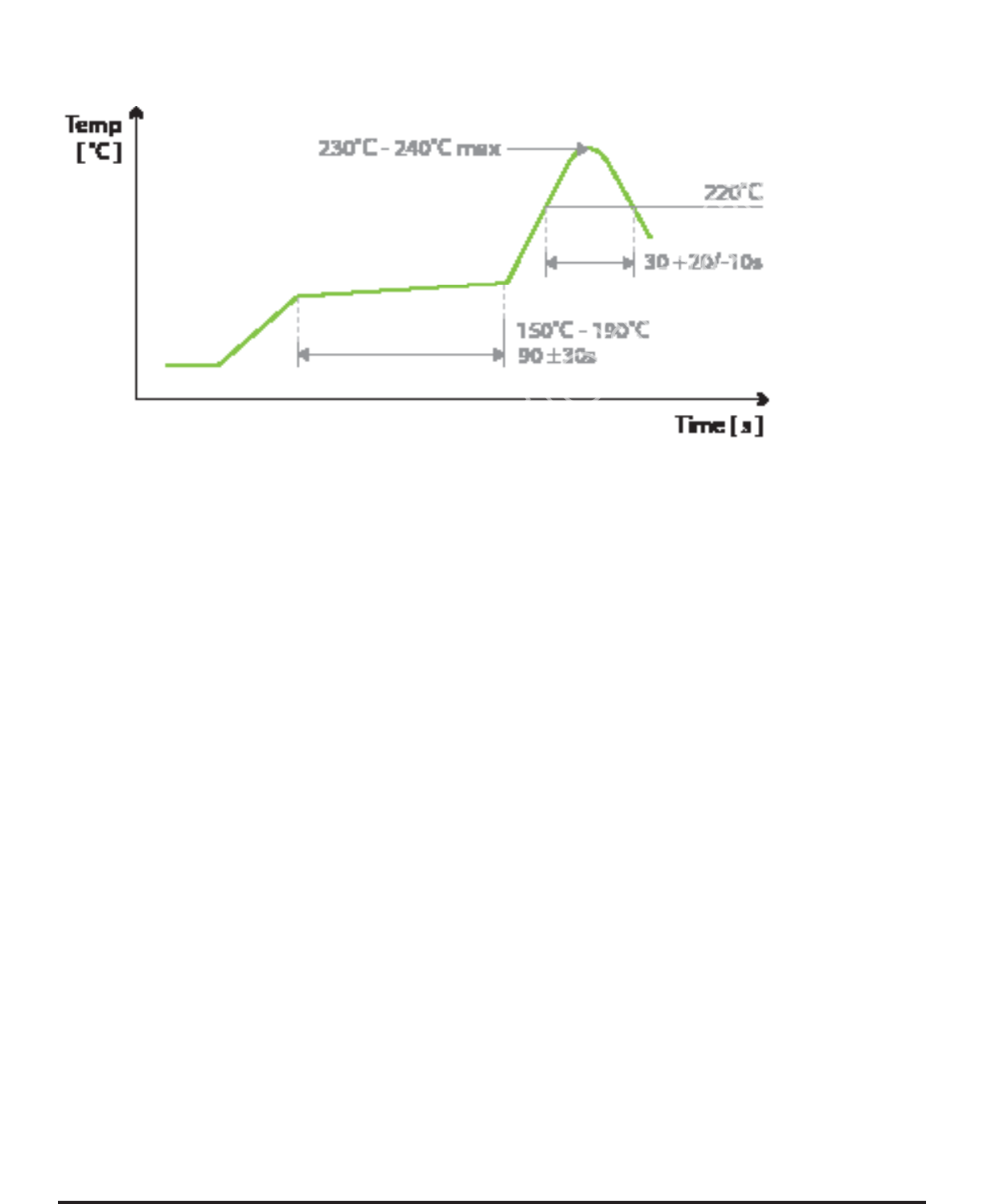
8 | Soldering Temperature Time Prole for reow soldering (Lead-free solder)
Maximum reow cycles: 2
Opposite-side reow is prohibited due to the module weight. You must not place the module on the bottom / underside
of your PCB and re-ow.
9 | Regulatory Approvals
9.1 | Federal Communications Commission (FCC - US)
Note: this section applies to CSB04PA10-CHP and CSB04PA10-RFC devices only.
9.1.1 | Approved Antennae
For the CSB04PA10-CHP modules using the onboard chip antenna, the approved 802.15.4 power level settings are
19.2 dBm for channels 11-25 and 15 dBm for channel 26. The approved BLE power level settings are 19.2dBm for both
connected and advertising modes. The onboard chip antenna is Inpaq ACA-2012-A1-CC-S with a gain of 1.72dBi and
50Ω impedance.
For the CSB04PA10-RFC modules using the approved external antenna, the approved 802.15.4 power level settings
are 19.2 dBm for channels 11-25 and 8 dBm for channel 26. The approved BLE power level settings are 19.2dBm
for connected mode and 15dBm for advertising modes. The CSB04PA1x-RFC devices have been approved with the
following external FCC approved antennas: Mag Layers EDA-1713-2G4C1-A2, and Bondale G-RA0K13200284-SZ478
with a gain of 5dBi and nominal impedance of 50Ω.
9.1.2 | FCC Notice
The CSB04PA1x-CHP and CSB04PA1x-RFC devices comply with Part 15 of the FCC rules. Operation is subject to the
following two conditions:
(1) This device may not cause harmful interference, and
(2) This device must accept any interference received, including interference that may cause undesired operation.
To comply with FCC RF Exposure requirements, users of this device must ensure that the module be installed and/or
congured to operate with a separation distance of 20cm or more from all persons.
Usage of Channel 26 at full power will result in non-compliance to FCC standards. MMB recommends avoiding use of
channel 26 and if necessary only use with a reduced power setting. For further details please contact MMB.
Preliminary Information

Page 12Rev 0.3 © MMB Networks 2018 CSB04PA1x Module Data Sheet
This equipment has been tested and found to comply with the limits for a Class B digital device, pursuant to Part 15 of
the FCC Rules. These limits are designed to provide reasonable protection against harmful interference in a residential
installation. This equipment generates, uses and can radiate radio frequency energy and, if not installed and used in
accordance with the instructions, may cause harmful interference to radio communications. However, there is no
guarantee that interference will not occur in a particular installation. If this equipment does cause harmful interference to
radio or television reception, which can be determined by turning the equipment o and on, the user is encouraged to try
to correct the interference by one of the following measures:
• Reorient or relocate the receiving antenna.
• Increase the separation between the equipment and receiver.
• Connect the equipment into an outlet on a circuit dierent from that to which the receiver is connected.
• Consult the dealer or an experienced radio/TV technician for help.
9.1.3 | Modular Approval
The CSB04PA1x-CHP and CSB04PA1x-RFC devices meet the requirements for modular transmitter approval as detailed in
the FCC public notice DA 00-1407.
It should be noted that:
“While the applicant for a device into which an authorized module is installed is not required to obtain a new authorization
for the module, this does not preclude the possibility that some other form of authorization or testing may be required for
the device (e.g., a WLAN into which an authorized module is installed must still be authorized as a PC peripheral, subject to
the appropriate equipment authorization).”
-- FCC Public Notice DA 00-1407
Caution:
Changes or modications not expressly approved by the party responsible for compliance could void the user’s authority
to operate the equipment.
NOTE:
This module is intended for an OEM integrator. The OEM integrator is responsible for the compliance to all the rules that
apply to the product into which this certied RF module is integrated. Additional testing and certication may be necessary
when multiple modules are used.
A 20cm minimum distance has to be able to be maintained between the antenna and the users for the host this
module is integrated into. Under such conguration, the FCC radiation exposure limits set forth for a population/
uncontrolled environment can be satised. Further RF exposure shall be re-evaluated to the scenario of portable, and
collocated use.
USER MANUAL OF THE END PRODUCT:
In the user manual of the end product, the end user has to be informed to keep at least 20cm separation with the antenna
while this end product is installed and operated. The end user has to be informed that the FCC radio-frequency exposure
guidelines for an uncontrolled environment can be satised.
The end user has to also be informed that any changes or modications not expressly approved by the manufacturer could
void the user’s authority to operate this equipment.
Preliminary Information
Page 13Rev 0.3 © MMB Networks 2018 CSB04PA1x Module Data Sheet
9.1.4 | Labeling Requirements
The user of this device is responsible for meeting the FCC labeling requirements. A clearly visible label on the exterior
enclosure of an incorporating device must list the MMB Research Inc. FCC ID “XFF-CSB04PA1X” and the FCC Notice above
(section 9.1.1).
The exterior label should use the wording “Contains” or “Contains Transmitter Module”. For example:
Contains FCC ID: XFF-CSB04PA1X
or
Contains Transmitter Module FCC ID: XFF-CSB04PA1X
Any similar wording that expresses the same meaning may be used. If the labelling area is smaller than the palm
of the hand, then additional FCC part 15.19 statement is required to be available in the users manual: This device
complies with Part 15 of FCC rules. Operation is subject to the following two conditions: (1) this device may not cause
harmful interference and (2) this device must accept any interference received, including interference that may cause
undesired operation.
LABEL OF THE END PRODUCT:
The nal end product must be labeled in a visible area with the following “Contains TX FCC ID: XFF-CSB04PA1X”.
If the labelling area is larger than the palm of the hand, then the following FCC part 15.19 statement has to also be
available on the label: This device complies with Part 15 of FCC rules. Operation is subject to the following two conditions:
(1) this device may not cause harmful interference and (2) this device must accept any interference received, including
interference that may cause undesired operation.
9.2 | Industry Canada (IC)
Note: this section applies to CSB04PA10-CHP and CSB04PA10-RFC devices only.
9.2.1 | Approved Antennae
This radio transmitter IC: 8365A-CSB04PA1X has been approved by Innovation, Science and Economic Development
Canada to operate with the antenna types listed below, with the maximum permissible gain indicated. Antenna
types not included in this list that have a gain greater than the maximum gain indicated for any type listed are strictly
prohibited for use with this device.
Antenna Type Manufacturer Model
Maximum Gain
(dBi)
Nominal
Impedance (Ω)
Integral Chip
Antenna Inpaq ACA-2012-A1-CC-S 1.72 50
Dipole Antenna
Mag-Layers
Scientic-Technics
Co. Ltd. EDA-1713-2G4C1-A2 5 50
Dipole Antenna Bondale G-RA0K13200284-SZ478 5 50
For the CSB04PA10-CHP modules using the onboard chip antenna, the approved 802.15.4 power level settings are
19.2 dBm for channels 11-25 and 15 dBm for channel 26. The approved BLE power level settings are 19.2dBm for both
connected and advertising modes.
For the CSB04PA10-RFC modules using the approved external antenna, the approved 802.15.4 power level settings
are 19.2 dBm for channels 11-25 and 8 dBm for channel 26. The approved BLE power level settings are 19.2dBm for
connected mode and 15dBm for advertising modes.
Preliminary Information

Page 14Rev 0.3 © MMB Networks 2018 CSB04PA1x Module Data Sheet
9.2.2 | IC Notice
This device complies with Industry Canada licence-exempt RSS standard(s).
Operation is subject to the following two conditions:
(1) this device may not cause interference, and
(2) this device must accept any interference, including interference that may cause undesired operation of the device.
Le présent appareil est conforme aux CNR d’Industrie Canada applicables aux appareils radio exempts de licence.
L’exploitation est autorisée aux deux conditions suivantes :
(1) l’appareil ne doit pas produire de brouillage, et
(2) l’utilisateur de l’appareil doit accepter tout brouillage radioélectrique subi, même si le brouillage est susceptible
d’en compromettre le fonctionnement.
9.2.3 | Labeling Requirements
The host device shall be properly labelled to identify the modules within the host device. The Industry Canada certication
label of a module shall be clearly visible at all times when installed in the host device, otherwise the host device must be
labelled to display the Industry Canada certication number of the module, preceded by the words “Contains transmitter
module”, or the word “Contains”, or similar wording expressing the same meaning, as follows:
Contains transmitter module IC: 8365A-CSB04PA1X
Contient le émetteur radio IC: 8365A-CSB04PA1X
9.2.4 | Additional Notice
This module is intended for an OEM integrator. The OEM integrator is responsible for the compliance to all the rules
that apply to the product into which this certied RF module is integrated. Additional testing and certication may be
necessary when multiple modules are used.
A 20cm minimum distance has to be able to be maintained between the antenna and the users for the host this
module is integrated into. Under such conguration, the FCC radiation exposure limits set forth for a population/
uncontrolled environment can be satised. Further RF exposure shall be re-evaluated to the scenario of portable, and
collocated use.
9.3 | RoHS Compliance
The CSB04PA1X devices do not contain any substances in excess of the maximum concentration allowed by Directive
2002/95/EC. The module is RoHS compliant.
9.4 | FCC & IC Compliance
In the event that conditions as described in the manual cannot be met, then the FCC and ISED authorizations are
no longer considered valid and the FCC ID and IC certication number cannot be used on the nal product. In these
circumstances, the integrator will be responsible for re-evaluating the end product (including the transmitter) and
obtaining a separate FCC and ISED authorization.
10 | Revision History
Revision Date Comments
0.3 2018/07/30
Added section 9 forregulatory statements for FCC&IC, Updated 5.2 to
include BLE transmit specications.
0.2 2018/05/xx Added BLE5.0 support, other minor typos.
0.1 2018/05/07 Initial draft
Preliminary Information
Page 15Rev 0.2 © MMB Networks 2018 CSB04PA1x Module Data Sheet
Copyright © 2018 MMB Research Inc. All rights reserved.
The information in this document is subject to change without notice. This document
is believed to be accurate and reliable, but the statements contained herein are
presented without expressed or implied warranty.
MMB Networks is a division of MMB Research Inc
RapidSE, RapidHA, and RapidConnect are trademarks of MMB Research Inc.
All other trademarks are the property of their respective holders.
May 2018
500 -243 College Street
Toronto, Ontario, Canada
M5T 1R5
416.636.3145
info@mmbnetworks.com
www.mmbnetworks.com
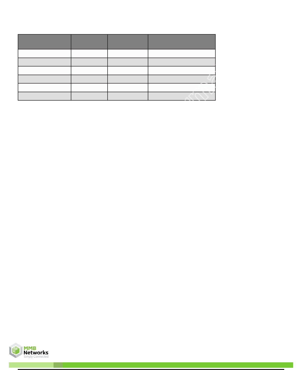
11 | Ordering Information
Hardware SKU
Regulatory
Approvals
RF Output
Option Status
CSB04PA10-CHP-N FCC/IC Chip Antenna Engineering Samples
CSB04PA10-PIN-X N/A1Module Pad 1 Engineering Samples
CSB04PA10-RFC-N FCC/IC RF Connector Engineering Samples
CSB04PA11-CHP-D FCC/IC, TBD Chip Antenna Engineering Samples
CSB04PA11-PIN-X N/A1Module Pad 1 Engineering Samples
CSB04PA11-RFC-D FCC/IC, TBD RF Connector Engineering Samples
Notes:
1. The PIN variant of the module has no regulatory approvals. Host manufacturers who decide to use this variant are
responsible for full certication of the product.
The above table provides the HW SKU which forms the rst part of the complete part number. The complete part number
takes the format: CSB04PA1x-yyy-r-zzz. Where r is the regulatory region (E=Europe, N=North America, D=Dual), and zzz
represents a three digit programming code.
Contact your local MMB sales representative to determine the correct programming code for your application.
Preliminary Information