MMB Research MMBPA10 RADPIDSE ZIGBEE SMART ENERGY User Manual
MMB Research Inc. RADPIDSE ZIGBEE SMART ENERGY Users Manual
UserManual.wiki
>
MMB Research
>
MMBPA10 User Manual
Users Manual
Navigation menu
Upload a User Manual
Namespaces
Wiki Guide
HTML
PDF
Info
Views
User Manual
Discussion / Help
Navigation
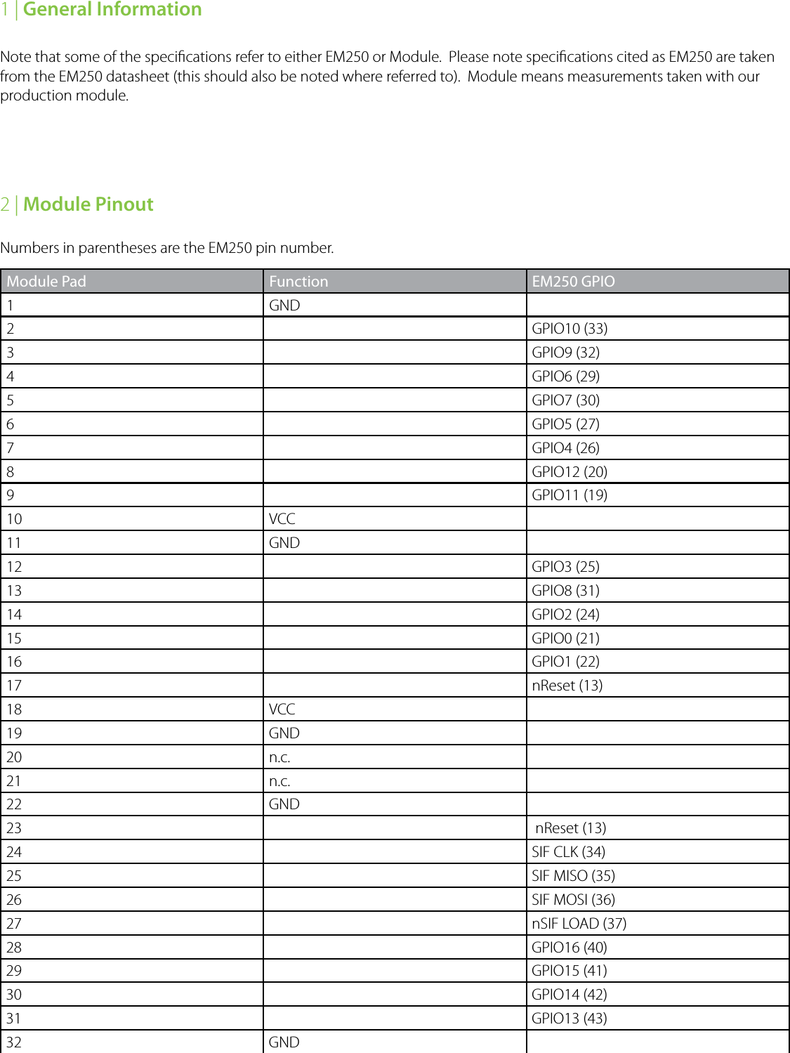
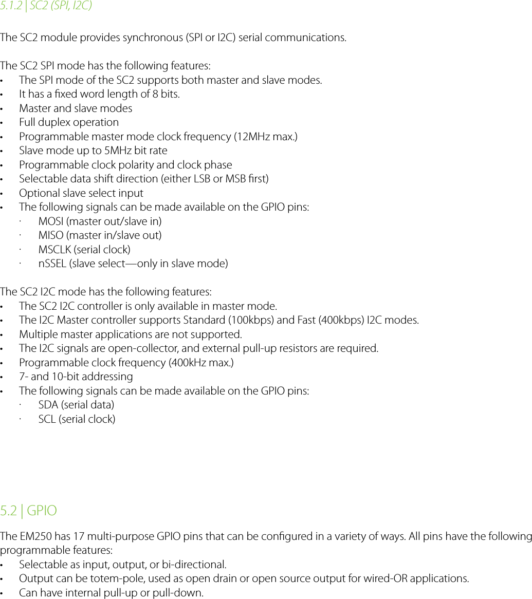
![3 | Electrical Specications3.1 | Absolute Maximum Ratings3.2 | Recommended Operating Conditions3.3 | DC Electrical CharacteristicsParameter Minimum Maximum UnitsSupply Voltage (VCC) -0.3 3.6 VVoltage on any GPIO[0:16], SIF CLK, SIF MISO, SIF MOSI, nSIE LOAD, nReset -0.3 VCC +0.3 VAmbient Operating Temperature -40 +75 °CStorage Temperature -40 +125 °CParameter Minimum Typical Maximum UnitsSupply Voltage (VCC) 2.7 3.3 3.6 VTemperature Range -40 +75 °CParameter Test Condition Minimum Typical Maximum UnitsOperating current(VCC = 3.3v)Average usage with radio in TX mode 27% of the time and RX mode 73% of the time61.4 mADeep sleep current At 25 °C, VCC = 3.3v, shutdown mode10.5 µAIdle current At 25 °C, VCC = 3.3v, sleep mode7.8 mARX current At 25 °C, VCC = 3.3v 36 mATX current At 25 °C, VCC = 3.3v, high power mode130 mA](https://usermanual.wiki/MMB-Research/MMBPA10/User-Guide-1183450-Page-3.png)