MMB Research MMBPA10 RADPIDSE ZIGBEE SMART ENERGY User Manual
MMB Research Inc. RADPIDSE ZIGBEE SMART ENERGY Users Manual
Users Manual

RapidSE ZigBee Smart Energy Module
RSE.ESP.MMB-PA.1.0, RSE.DVC.MMB-PA.1.0 Rev 1.2
The RapidSE Module is a drop-in ZigBee Smart Energy solution.
Preloaded with MMB Research’s RapidSE ZigBee Smart Energy
application, it offers hardware vendors an easy way to integrate
a fully-implemented ZigBee Smart Energy platform into their
existing devices.
MMB Research offers a variety of hardware and software
development tools to facilitate integration. For more
information, please visit http://www.mmbresearch.com
Contents
1 | General Information 2
2 | Module Pinout 2
3 | Electrical Specications 3
3.1 | Absolute Maximum Ratings 3
3.2 | Recommended Operating Conditions 3
3.3 | DC Electrical Characteristics 3
4 | RF Specications 4
4.1 | Receive Specifications 4
4.2 | Transmit Specifications 5
4.3 | Synthesizer 5
5 | Functional Specications 6
5.1 | Serial Ports 6
5.2 | GPIO 7
5.3 | Analog to Digital Converter (ADC) 8
6 | Mechanical Specications 9
6.1 | Physical Dimensions 9
6.2 | Recommended Land Pattern (Surface Mount) 10
6.3 | Connector Specifications 11
6.4 | Labelling 11
7 | Regulatory Approvals 11
7.1 | FCC 11

1 | General Information
Note that some of the specifications refer to either EM250 or Module. Please note specifications cited as EM250 are taken
from the EM250 datasheet (this should also be noted where referred to). Module means measurements taken with our
production module.
Numbers in parentheses are the EM250 pin number.
Module Pad Function EM250 GPIO
1 GND
2 GPIO10 (33)
3 GPIO9 (32)
4 GPIO6 (29)
5 GPIO7 (30)
6 GPIO5 (27)
7 GPIO4 (26)
8 GPIO12 (20)
9 GPIO11 (19)
10 VCC
11 GND
12 GPIO3 (25)
13 GPIO8 (31)
14 GPIO2 (24)
15 GPIO0 (21)
16 GPIO1 (22)
17 nReset (13)
18 VCC
19 GND
20 n.c.
21 n.c.
22 GND
23 nReset (13)
24 SIF CLK (34)
25 SIF MISO (35)
26 SIF MOSI (36)
27 nSIF LOAD (37)
28 GPIO16 (40)
29 GPIO15 (41)
30 GPIO14 (42)
31 GPIO13 (43)
32 GND
2 | Module Pinout
3 | Electrical Specications
3.1 | Absolute Maximum Ratings
3.2 | Recommended Operating Conditions
3.3 | DC Electrical Characteristics
Parameter Minimum Maximum Units
Supply Voltage (VCC) -0.3 3.6 V
Voltage on any GPIO[0:16], SIF CLK, SIF MISO, SIF MOSI, nSIE LOAD, nReset -0.3 VCC +0.3 V
Ambient Operating Temperature -40 +75 °C
Storage Temperature -40 +125 °C
Parameter Minimum Typical Maximum Units
Supply Voltage (VCC) 2.7 3.3 3.6 V
Temperature Range -40 +75 °C
Parameter Test Condition Minimum Typical Maximum Units
Operating current
(VCC = 3.3v)
Average usage with radio
in TX mode 27% of the
time and RX mode 73% of
the time
61.4 mA
Deep sleep current At 25 °C, VCC = 3.3v,
shutdown mode
10.5 µA
Idle current At 25 °C, VCC = 3.3v, sleep
mode
7.8 mA
RX current At 25 °C, VCC = 3.3v 36 mA
TX current At 25 °C, VCC = 3.3v, high
power mode
130 mA
4 | RF Specications
4.1 | Receive Specifications
Table 4.1 | Module Receive Characteristics
Table 4.2 | Receive Strength Signal Indicator (RSSI) Accuracy
Table 4.3 | EM250 Receive Characteristics
Parameter Test Condition Min Typical Max Units
Receive sensitivity Max gain -97.56 dBm
Receive sensitivity (Boost) Max gain -99.53 dBm
Input 1dB Compression CW +26 dBm
Input IP3 Two -7 dBm CW tones spaced 1 MHz apart +36 dBm
Parameter Test Condition Minimum Typical Maximum Units
Frequency range 2400 2500 MHz
Sensitivity (Boost mode) 1% PER, 20 byte packet
defined by IEEE 802.15.4
-100 -95 dBm
Sensitivity 1% PER, 20 byte packet
defined by IEEE 802.15.4
-99 -94 dBm
High-side adjacent channel rejection IEEE 802.15.4 signal at -82dBm 35 dB
Low-side adjacent channel rejection IEEE 802.15.4 signal at -82dBm 35 dB
2nd high-side adjacent channel rejection IEEE 802.15.4 signal at -82dBm 43 dB
2nd low-side adjacent channel rejection IEEE 802.15.4 signal at -82dBm 43 dB
Channel rejection for all other channels IEEE 802.15.4 signal at -82dBm 40 dB
802.11g rejection centered at +12MHz or
-13MHz
IEEE 802.15.4 signal at -82dBm 35 dB
Maximum input signal level for correct
operation (low gain)
0 dBm
Image suppression 30 dB
Co-channel rejection IEEE 802.15.4 signal at -82dBm -6 dBc
Channel Actual Level Measured RSSI
18 -40 -40.0
18 -50 -50.0
18 -60 -60.0
18 -70 -70.0
18 -80 -79.0
18 -90 -89.2
Table 4.3 lists the key parameters of the integrated IEEE 802.15.4 receiver on the EM250. This information is taken from the Ember
EM250 Datasheet. Link to this document can be found in the References section.
Note: Receive Measurements were collected with Ember’s EM250 Lattice Balun Reference Design (Version B1) at 2440MHz and using
the EmberZNet software stack Version 3.0.1. The Typical number indicates one standard deviation above the mean, measured at room
temperature (25C). The Min and Max numbers were measured over process corners at room temperature.
Parameter Test Condition Minimum Typical Maximum Units
Relative frequency error
(2x40 ppm required by IEEE 802.15.4)
-120 +120 ppm
Relative timing error
(2x40 ppm required by IEEE 802.15.4)
-120 +120 ppm
Linear RSSI range 40 dB
RSSI Range -90 -30 dB
Table 4.3 | Continued
4.2 | Transmit Specifications
4.3 | Synthesizer
Table 4.4 | Module Transmitter Parameters
Table 4.5 | EM250 Synthesizer Parameters
Parameter Test Condition Min Typical Max Units
Maximum output power
(Boost mode)
At highest power setting 20.45 dBm
Output power (low
power PA mode)
At lower power PA setting ???
Carrier frequency error -40 -10 +40 ppm
PSD mask relative 3.5 MHz away -20 dB
PSD mask absolute 3.5 MHz away -30 dBm
Parameter Test Condition Min Typical Max Units
Frequency range 2400 2500 MHz
Frequency resolution 11.7 kHz
Lock time From off, with correct VCO DAC setting 100 us
Relock time Channel change or Rx/Tx turnaround (IEEE
802.15.4 defines 192μs turnaround time)
100 us
Phase noise at 100kHz -71 dBc/Hz
Phase noise at 1MHz -91 dBc/Hz
Phase noise at 4MHz -103 dBc/Hz
Phase noise at 10MHz -111 dBc/Hz
Table 4.5 lists the key parameters of the integrated synthesizer on the EM250. Taken from the EM250 datasheet.
5 | Functional Specications
5.1 | Serial Ports
5.1.1 | SC1 (UART, SPI, I2C)
Refer to the EM250 data sheet for functionality and associated GPIO pin outs.
Note: The module pin out table in section 2 of this document provides a cross reference between the MMB PA module
pins and the EM250 GPIO.
The SC1 module provides asynchronous (UART) or synchronous (SPI or I2C) serial communications.
The UART mode contains the following features:
• Baud rate (300bps up to 921kbps)
• Data bits (7 or 8)
• Parity bits (none, odd, or even)
• Stop bits (1 or 2)
• GPIO signals:
ʳ TXD
ʳ RXD
ʳ nRTS (optional)
ʳ nCTS (optional)
The SPI mode has the following features:
• Full duplex operation
• Programmable clock frequency (12MHz max.)
• Programmable clock polarity and clock phase
• Selectable data shift direction (either LSB or MSB first)
• Master mode only
• Fixed 8 bit word length
• The following signals can be made available on the GPIO pins:
ʳ MO (master out)
ʳ MI (master in)
ʳ MCLK (serial clock)
The SC1 I2C mode has the following features:
• Programmable clock frequency (400kHz max.)
• Supports both 7-bit and 10-bit addressing
• The SC1 I2C controller is only available in master mode.
• The I2C Master controller supports Standard (100kbps) and Fast (400kbps) I2C modes.
• Multiple master applications are not supported.
• The I2C signals are open-collector and external pull-up resistors are required.
• The following signals can be made available on the GPIO pins:
ʳ MSDA (serial data)
ʳ MSCL (serial clock)
5.1.2 | SC2 (SPI, I2C)
The SC2 module provides synchronous (SPI or I2C) serial communications.
The SC2 SPI mode has the following features:
• The SPI mode of the SC2 supports both master and slave modes.
• It has a fixed word length of 8 bits.
• Master and slave modes
• Full duplex operation
• Programmable master mode clock frequency (12MHz max.)
• Slave mode up to 5MHz bit rate
• Programmable clock polarity and clock phase
• Selectable data shift direction (either LSB or MSB first)
• Optional slave select input
• The following signals can be made available on the GPIO pins:
ʳ MOSI (master out/slave in)
ʳ MISO (master in/slave out)
ʳ MSCLK (serial clock)
ʳ nSSEL (slave select—only in slave mode)
The SC2 I2C mode has the following features:
• The SC2 I2C controller is only available in master mode.
• The I2C Master controller supports Standard (100kbps) and Fast (400kbps) I2C modes.
• Multiple master applications are not supported.
• The I2C signals are open-collector, and external pull-up resistors are required.
• Programmable clock frequency (400kHz max.)
• 7- and 10-bit addressing
• The following signals can be made available on the GPIO pins:
ʳ SDA (serial data)
ʳ SCL (serial clock)
5.2 | GPIO
The EM250 has 17 multi-purpose GPIO pins that can be configured in a variety of ways. All pins have the following
programmable features:
• Selectable as input, output, or bi-directional.
• Output can be totem-pole, used as open drain or open source output for wired-OR applications.
• Can have internal pull-up or pull-down.

5.3 | Analog to Digital Converter (ADC)
The ADC is a first-order sigma-delta converter sampling at 1MHz with programmable resolution and conversion
rate. the ADC Module supports both single-ended and differential inputs.
Parameter Minimum Typical Maximum Units
Conversion time 32 4096 µ S
VREF 1.19 1.2 1.21 V
VREF output current 1 mA
VREF load capacitance 10 nF
Minimum input voltage 0 V
Maximum input voltage VCC V
Single-ended signal range 0 VREF V
Differential signal range - VREF + VREF V
Common mode range 0 VREF V
Input referred ADC offset -10 10 mV
Input impedance
When taking a sample 1 M Ohm
When not taking a sample 10 M Ohm
INL -0.5 0.5 LSB
DNL -0.5 0.5 LSB
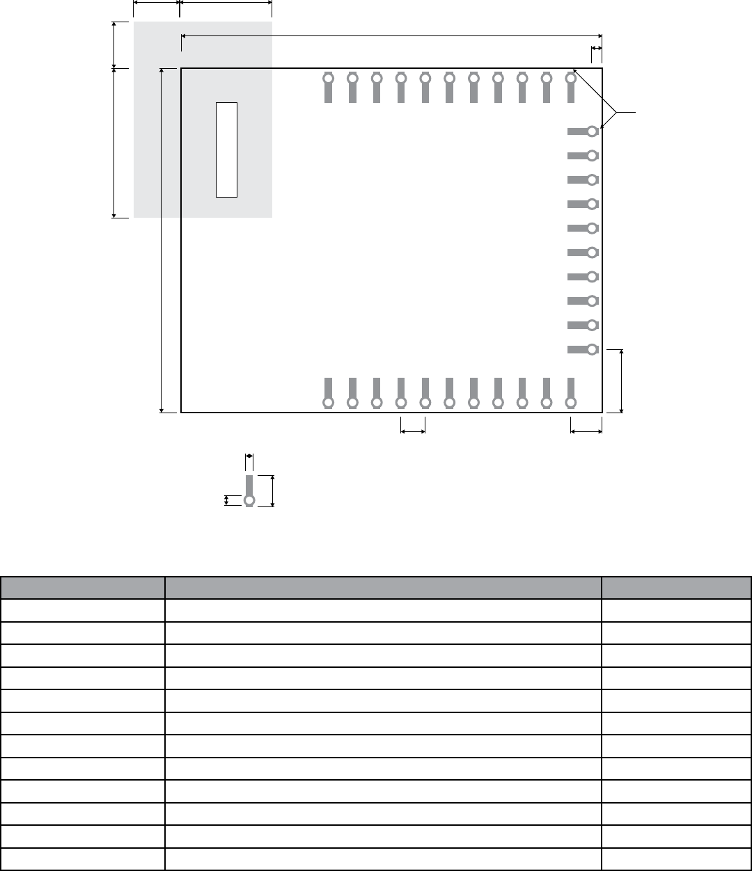
6.1 | Physical Dimensions
Symbol Description Distance
L Length of the module 34.73 mm
W Width of the module 28.43 mm
H Height of the module TBD
A1 Pitch 2 mm
A2 Distance centre of pad to PCB edge 2.59 mm
A3 Distance center of pad to PCB edge 5.22 mm
A4 Distance pad edge to PCB edge 0.29 mm
A5 Distance center of via to PCB edge 0.84 mm
R1 Keep-out zone from corner of PCB TBD
R2 Keep-out zone from corner of PCB TBD
R3 Width of keep-out zone TBD
R4 Length of keep-out zone TBD
1 11
32 22
12
21
A5
L
W
A4
A2
A3
A1
2.6 mm
0.6 mm
0.8 mm
R2
R1 R4
R3
A
N
T
E
N
N
A
6 | Mechanical Specications
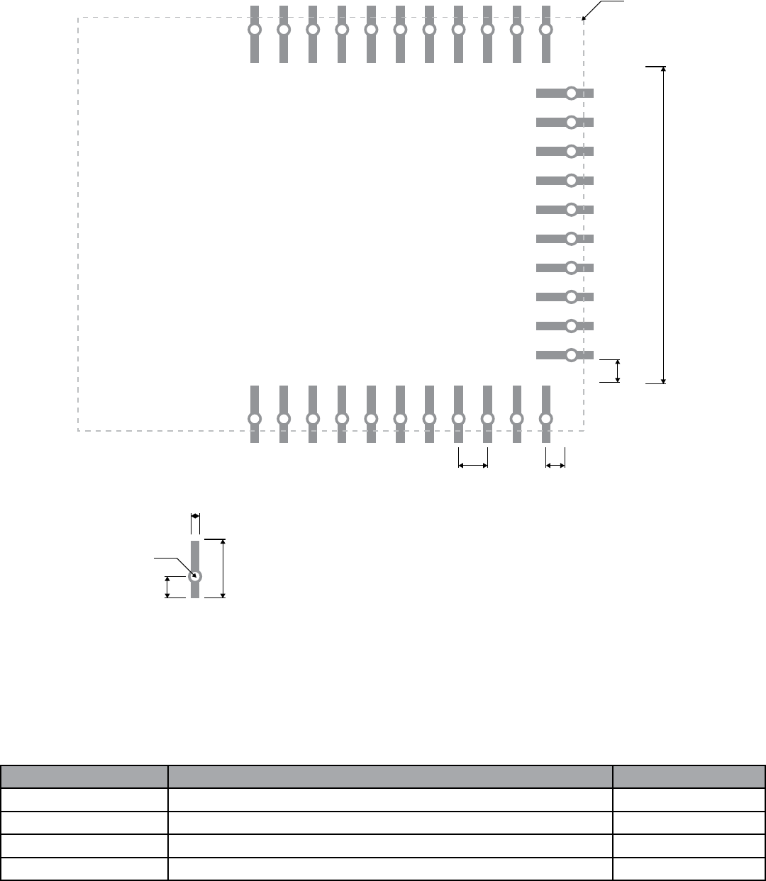
Symbol Description Distance
F1 Distance pad edge to pad edge 21.9 mm
F2 Distance pad edge to pad edge 1.523 mm
F3 Distance pad center to pad center 1.3 mm
F4 Pitch 2 mm
1 11
32 22
12
21
F1
F2
1.51 mm
3.94 mm
0.854 mm
d = 0.8 mm
F4 F3
module outline
6.2 | Recommended Land Pattern (Surface Mount)
Note: It is advised that for surface mount applications, through holes / vias should not be designed into the carrier board.
6.3 | Connector Specifications
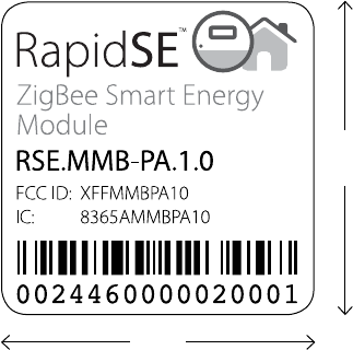
6.4 | Labelling
6.3.1 | Edge Mount (USNAP) Connector
7.1.1 | FCC Notice
6.3.2 | SIP Header / Socket
10 pin 2mm pitch right angle female header
11 + 11 + 10 (if no USNAP populated) pin 2mm pitch 0.8mm diameter through hole footprint
0.75”
0.75”
7.1 | FCC
7 | Regulatory Approvals
This device (ZGB.MMB-PA.1.0/ZGB.MMB-PA-LNA.1.0) complies with Part 15 of the FCC rules. Operation is subject to the
following two conditions:
(1) This device may not cause harmful interference, and
(2) This device must accept any interference received, including interference that may cause undesired operation.
To comply with FCC RF Exposure requirements, users of this device must ensure that the module be installed and/or
configured to operate with a separation distance of 20cm or more from all persons.

Rev 1.0 | 22.12.08
35 Prince Arthur Ave.
Toronto, Ontario, Canada
M5R1B2
416.636.3145
info@mmbresearch.com
www.mmbresearch.com
7.1.3 | Labeling Requirements
The user of this device is responsible for meeting the FCC labeling requirements. A clearly visible label on the exterior
enclosure of an incorporating device must list the MMB Research Inc. FCC ID “XFFMMBPA10” and the FCC Notice above
(section 7.1.1).
Devices intended for sale in the Canadian market should also include the Industry Canada (IC) ID “8365A-MMBPA10”
7.1.2 | Modular Approval
This device (ZGB.MMB-PA.1.0/ZGB.MMB-PA-LNA.1.0) meets the requirements for modular transmitter approval as detailed in
the FCC public notice DA 00-1407.
It should be noted that:
“While the applicant for a device into which an authorized module is installed is not required to obtain a new authorization
for the module, this does not preclude the possibility that some other form of authorization or testing may be required for
the device (e.g., a WLAN into which an authorized module is installed must still be authorized as a PC peripheral, subject to
the appropriate equipment authorization).”
-- FCC Public Notice DA 00-1407
Caution:
Changes or modifications not expressly approved by the party responsible for compliance could void the user’s authority
to operate the equipment.